EP2302402A1 - Stromsensor - Google Patents
Stromsensor Download PDFInfo
- Publication number
- EP2302402A1 EP2302402A1 EP09794130A EP09794130A EP2302402A1 EP 2302402 A1 EP2302402 A1 EP 2302402A1 EP 09794130 A EP09794130 A EP 09794130A EP 09794130 A EP09794130 A EP 09794130A EP 2302402 A1 EP2302402 A1 EP 2302402A1
- Authority
- EP
- European Patent Office
- Prior art keywords
- hall element
- current sensor
- circuit board
- core
- cabinet
- Prior art date
- Legal status (The legal status is an assumption and is not a legal conclusion. Google has not performed a legal analysis and makes no representation as to the accuracy of the status listed.)
- Withdrawn
Links
- 230000004907 flux Effects 0.000 claims abstract description 10
- 239000011810 insulating material Substances 0.000 claims abstract description 8
- 239000003990 capacitor Substances 0.000 claims description 13
- 239000000853 adhesive Substances 0.000 claims description 3
- 230000001070 adhesive effect Effects 0.000 claims description 3
- 230000005611 electricity Effects 0.000 abstract description 23
- 230000003068 static effect Effects 0.000 abstract description 22
- 239000004020 conductor Substances 0.000 description 11
- 230000000593 degrading effect Effects 0.000 description 8
- 238000012546 transfer Methods 0.000 description 7
- 238000009413 insulation Methods 0.000 description 6
- 238000003780 insertion Methods 0.000 description 4
- 230000037431 insertion Effects 0.000 description 4
- 238000012986 modification Methods 0.000 description 3
- 230000004048 modification Effects 0.000 description 3
- 229910000976 Electrical steel Inorganic materials 0.000 description 2
- 238000007796 conventional method Methods 0.000 description 2
- 230000000694 effects Effects 0.000 description 2
- 238000000034 method Methods 0.000 description 2
- 229910000889 permalloy Inorganic materials 0.000 description 2
- 229910000859 α-Fe Inorganic materials 0.000 description 2
- RYGMFSIKBFXOCR-UHFFFAOYSA-N Copper Chemical compound [Cu] RYGMFSIKBFXOCR-UHFFFAOYSA-N 0.000 description 1
- XUIMIQQOPSSXEZ-UHFFFAOYSA-N Silicon Chemical compound [Si] XUIMIQQOPSSXEZ-UHFFFAOYSA-N 0.000 description 1
- BQCADISMDOOEFD-UHFFFAOYSA-N Silver Chemical compound [Ag] BQCADISMDOOEFD-UHFFFAOYSA-N 0.000 description 1
- 230000002411 adverse Effects 0.000 description 1
- 239000011231 conductive filler Substances 0.000 description 1
- 229910052802 copper Inorganic materials 0.000 description 1
- 239000010949 copper Substances 0.000 description 1
- 238000001514 detection method Methods 0.000 description 1
- PCHJSUWPFVWCPO-UHFFFAOYSA-N gold Chemical compound [Au] PCHJSUWPFVWCPO-UHFFFAOYSA-N 0.000 description 1
- 230000005389 magnetism Effects 0.000 description 1
- 239000011347 resin Substances 0.000 description 1
- 229920005989 resin Polymers 0.000 description 1
- 230000035945 sensitivity Effects 0.000 description 1
- 229910052710 silicon Inorganic materials 0.000 description 1
- 239000010703 silicon Substances 0.000 description 1
Images
Classifications
-
- G—PHYSICS
- G01—MEASURING; TESTING
- G01R—MEASURING ELECTRIC VARIABLES; MEASURING MAGNETIC VARIABLES
- G01R15/00—Details of measuring arrangements of the types provided for in groups G01R17/00 - G01R29/00, G01R33/00 - G01R33/26 or G01R35/00
- G01R15/14—Adaptations providing voltage or current isolation, e.g. for high-voltage or high-current networks
- G01R15/20—Adaptations providing voltage or current isolation, e.g. for high-voltage or high-current networks using galvano-magnetic devices, e.g. Hall-effect devices, i.e. measuring a magnetic field via the interaction between a current and a magnetic field, e.g. magneto resistive or Hall effect devices
- G01R15/202—Adaptations providing voltage or current isolation, e.g. for high-voltage or high-current networks using galvano-magnetic devices, e.g. Hall-effect devices, i.e. measuring a magnetic field via the interaction between a current and a magnetic field, e.g. magneto resistive or Hall effect devices using Hall-effect devices
-
- G—PHYSICS
- G01—MEASURING; TESTING
- G01R—MEASURING ELECTRIC VARIABLES; MEASURING MAGNETIC VARIABLES
- G01R15/00—Details of measuring arrangements of the types provided for in groups G01R17/00 - G01R29/00, G01R33/00 - G01R33/26 or G01R35/00
- G01R15/14—Adaptations providing voltage or current isolation, e.g. for high-voltage or high-current networks
- G01R15/20—Adaptations providing voltage or current isolation, e.g. for high-voltage or high-current networks using galvano-magnetic devices, e.g. Hall-effect devices, i.e. measuring a magnetic field via the interaction between a current and a magnetic field, e.g. magneto resistive or Hall effect devices
- G01R15/207—Constructional details independent of the type of device used
Definitions
- the present invention relates to a current sensor, and more specifically, relates to a technique for protecting a current sensor using a Hall element from static electricity.
- FIG. 5 illustrates an example of a conventional current sensor using a Hall element.
- the current sensor 30 of FIG. 5 comprises a Hall element 31, a core (magnetic body) 32, a circuit board 33 to which the Hall element 31 is attached, and a cabinet 34.
- the core 32 is a ring-shaped component having inside a conductor insertion portion 32a through which a conductor (not illustrated), through which a target current flows, is inserted.
- a gap 32b Provided at a part of the ring is a gap 32b where the Hall element 31 is disposed.
- the core 32 is formed of a magnetic body with small magnetic resistance such as ferrite, a silicon steel sheet, and permalloy, and serves to collect interlinkage magnetic flux generated around the above conductor inserted through the conductor insertion portion 32a.
- the Hall element 31 outputs an electric signal (voltage) corresponding to the amount of the magnetic flux collected by the core 32.
- an amplifier circuit (not illustrated) for amplifying the output signal from the Hall element 31 is disposed on the circuit board 33.
- a protection element 35 in the form of a capacitor, a Zener diode, or the like is provided on the circuit board 33.
- the protection element 35 is for protecting the components (e.g., the above amplifier circuit) inside the current sensor 30 from static electricity applied via a supply line for the drive power which drives the Hall element 31 and the above amplifier circuit.
- PTL 1 discloses a technique for protecting electronic equipments from extraneous surges that come through a power line.
- a current sensor using a Hall element is used in various fields, and is also useful in that it can safely measure currents of power sources having characteristics of high voltage and high output, particularly due to its high insulation for the target currents. Due to such a reason, a current sensor using a Hall element is also used for measuring output currents of battery packs serving as the power source for driving hybrid vehicles.
- Such battery packs are assembled of a plurality of secondary batteries connected to one another so as to obtain high voltage and high output, and sufficient care is required for their handling, since, while having characteristics of high voltage and high output, the current that flows out and the amount of heat generated are large when there is an electricity leakage.
- its cabinet is preferably made of an insulating material.
- the cabinet is made of an insulating material, static electricity generated outside may transfer to the wall portion of the cabinet and then to the core.
- insulation between the core and the Hall element is usually secured by a gap therebetween. Since the gap between the core and the Hall element needs to be as small as possible to increase sensitivity of the Hall element, there may be contact between the core and the Hall element, caused due to variation in production of the current sensors. In such a case, there is the problem of the properties of the Hall element degrading due to static electricity which has transferred from the wall portion of the cabinet to the core, subsequently transferring to the Hall element.
- An object of the present invention which is made in view of the above problem, is to provide a current sensor capable of preventing a Hall element therein from degrading due to static electricity.
- a current sensor of the present invention comprises: a magnetic body for collecting magnetic flux generated by a target current; a Hall element for outputting an electric signal corresponding to the amount of the magnetic flux collected by the magnetic body; an amplifier for amplifying the output signal from the Hall element; and a circuit board to which the Hall element and the amplifier are attached, the current sensor having a conducting means for allowing conduction between the magnetic body and the circuit board.
- the conducting means preferably comprises at least one selected from the group consisting of a resistor, a capacitor, a diode, and a varistor.
- the conducting means also preferably comprises a conductive adhesive.
- a cabinet comprising an insulating material for accommodating the magnetic body, the Hall element, the amplifier, and the circuit board, is also preferably provided.
- the conducting means since there is conduction between the magnetic body and the circuit board by the conducting means, even when static electricity generated outside transfers to the magnetic body from the wall portion of the cabinet being an insulating body, such static electricity can be transferred to the circuit board via the conductive means. Therefore, static electricity exceeding a specified level is prevented from being applied to the Hall element from the magnetic body. This can prevent the properties of the Hall element from degrading.
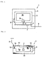
- FIG. 1 is a front view of a current sensor according to an embodiment of the present invention, seen through a cabinet thereof.
- FIG. 2 is a plan view of a circuit board in the apparatus of FIG. 1 .
- the current sensor 1 of FIG. 1 comprises a Hall element 2, a core (magnetic body) 3, the circuit board 4, and a cabinet 5 made of an insulating material.
- the core 3 is a ring-shaped component having inside a conductor insertion portion 3a through which a conductor (not illustrated), through which a target current flows, is inserted.
- a gap 3b Provided at a part of the ring is a gap 3b where the Hall element 2 is disposed.
- the core 3 is formed of a magnetic body with small magnetic resistance such as ferrite, a silicon steel sheet, and permalloy, and serves as a magnetism collecting means for collecting interlinkage magnetic flux generated around the above conductor due to the current in the above conductor.
- the Hall element 2 outputs an electric signal for voltage corresponding to the amount of the magnetic flux collected by the core 3.
- Attached to the circuit board 4 is the Hall element 2, and also an amplifier circuit 6 for amplifying the output signal from the Hall element 2.
- the circuit board 4 has a connecting wire 4a of a connecting line 9 that will be described below, a grounding wire 4b, and a power supply wire 4c.
- a protection element 7 in the form of a capacitor, a Zener diode, or the like is provided on the circuit board 4.
- the protection element 7 is for protecting the amplifier circuit 6, etc. from static electricity applied via a supply line 8 for the drive power to drive the Hall element 2 and the amplifier circuit 6.
- the current sensor 1 comprises a connecting line 9 which allows conduction between the core 3 and the circuit board 4, in order for static electricity which has transferred from the cabinet 5, etc. to the core 3, to subsequently transfer to the circuit board 4.
- the connecting line 9 is connected to the connecting wire 4a provided on the circuit board 4.
- the connecting line 9 is connected to the core 3 and the connecting wire 4a with a conductive adhesive, in which a conductive filler of a gold powder, a silver powder, a copper power, or the like is closely packed inside a resin.
- the connecting wire 4a is preferably connected, for example, to the grounding wire 4b via a resistor 10. This enables static electricity from the core 3 to escape via the connecting line 9, the connecting wire 4a, the resistor 10, and the grounding wire 4b.
- allowing static electricity from the core 3 to escape via the resistor 10 is to adjust so that voltage generated when static electricity flows through the resistor 10 does not exceed the withstand voltage of the Hall element 2.
- the resistance value of the resistor 10 can be selected as appropriate from the range of, for example, 0.1 to 100 ⁇ . This is because the desired resistance value of the resistor 10 would be 1.8 ⁇ , assuming that static electricity of the human body model is usually 1.5 k ⁇ , withstand voltage of the Hall element is 30 V, and electrostatic charge of 25 kV is present.
- the resistor used for the resistor 10 is preferably a resistive element having excellent electrostatic capacity.
- the resistor 10 when using a Hall element with an extremely low withstand voltage as the Hall element 2, it may be necessary to make the resistance value of the resistor 10 smaller than the lower limit of the above range, depending on that withstand voltage.
- Embodiment 2 is a modification of Embodiment 1, and the following describes only the part differing from Embodiment 1.
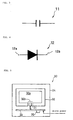
- a capacitor 11 instead of the resistor 10, a capacitor 11 as illustrated in FIG. 3 is disposed between the connecting wire 4a and the grounding wire 4b.
- the capacity of the capacitor 11 can be selected as appropriate from the range of, for example, 0.01 to 1 ⁇ F. This is because the desired capacity of the capacitor 11 would be about 0.1 ⁇ F, assuming that static electricity of the human body model is usually 150 pF, withstand voltage of the Hall element is 30 V, and electrostatic charge of 25 kV is present. As such, even when the capacitor 11 is disposed between the connecting wire 4a and the grounding wire 4b instead of the resistor 10, voltage applied to the Hall element 2 by way of the core 3 can be made sufficiently lower than the withstand voltage of the Hall element 2, and the Hall element 2 can be prevented from degrading.
- Embodiment 3 is a modification of Embodiment 1, and the following only describes the part differing from Embodiment 1.
- a diode 12 as illustrated in FIG. 4 is disposed between the connecting wire 4a and the grounding wire 4b. At this time, the anode terminal of the diode 12 is connected to the connecting wire 4a, and the cathode terminal thereof is connected to the grounding wire 4b.
- any two of the resistor 10, the capacitor 11, the diode 12, and the varistor, or, in the alternative, all of the above, may be disposed between the connecting wire 4a and the grounding wire 4b.
- the conductive wire 4a and the grounding wire 4b may be connected simply by a conductive line. Cost reduction is possible in this case, since circuit components such as the resistor, the capacitor, etc. can be omitted.
- circuit components such as the resistor, the capacitor, etc. can be omitted.
- the connecting wire 4a and the grounding wire 4b are connected directly to each other, preferably only in the case where countermeasures can be taken to avoid such a disadvantage.
- the connecting wire 4a that is, the connecting line 9 may be connected to the power supply wire 4c which supplies power to the amplifier circuit 6 and the Hall element 2.
- a low voltage e.g., 5V
- the Hall element 2 is not adversely affected even when a voltage of such level is applied to the core 3 via the connecting line 9, etc.
- the connecting wire 4a and the grounding wire 4b are simply connected by a conductive line, as described above.
- the present invention when the cabinet is made of an insulating material for increased insulation, the properties of the Hall element can be prevented from degrading due to static electricity which transfers from the cabinet to the core. Therefore, the present invention is useful as a current sensor for measuring currents of power sources, particularly of those having characteristics of high voltage and high output.
Landscapes
- Physics & Mathematics (AREA)
- General Physics & Mathematics (AREA)
- Measuring Instrument Details And Bridges, And Automatic Balancing Devices (AREA)
Applications Claiming Priority (2)
| Application Number | Priority Date | Filing Date | Title |
|---|---|---|---|
| JP2008178046A JP2010019586A (ja) | 2008-07-08 | 2008-07-08 | 電流センサ |
| PCT/JP2009/002446 WO2010004682A1 (ja) | 2008-07-08 | 2009-06-02 | 電流センサ |
Publications (1)
| Publication Number | Publication Date |
|---|---|
| EP2302402A1 true EP2302402A1 (de) | 2011-03-30 |
Family
ID=41506810
Family Applications (1)
| Application Number | Title | Priority Date | Filing Date |
|---|---|---|---|
| EP09794130A Withdrawn EP2302402A1 (de) | 2008-07-08 | 2009-06-02 | Stromsensor |
Country Status (4)
| Country | Link |
|---|---|
| US (1) | US20110101958A1 (de) |
| EP (1) | EP2302402A1 (de) |
| JP (1) | JP2010019586A (de) |
| WO (1) | WO2010004682A1 (de) |
Cited By (1)
| Publication number | Priority date | Publication date | Assignee | Title |
|---|---|---|---|---|
| EP2546660A1 (de) * | 2011-07-13 | 2013-01-16 | LEM Intellectual Property SA | Stromsensor mit geerdetem Magnetkern |
Families Citing this family (6)
| Publication number | Priority date | Publication date | Assignee | Title |
|---|---|---|---|---|
| CN102646437A (zh) * | 2011-02-17 | 2012-08-22 | 鸿富锦精密工业(深圳)有限公司 | 电子装置 |
| US9651581B2 (en) * | 2011-09-28 | 2017-05-16 | Infineon Technologies Ag | High current sensors |
| JP6294034B2 (ja) * | 2013-09-05 | 2018-03-14 | ルネサスエレクトロニクス株式会社 | センサ装置 |
| WO2018155701A1 (ja) * | 2017-02-27 | 2018-08-30 | Tdk株式会社 | 磁気センサ |
| CN107703341A (zh) * | 2017-09-08 | 2018-02-16 | 佛山市南海毅顺电器设备有限公司 | 一种用于测量母排直流大电流的装置 |
| JP2019054017A (ja) * | 2017-09-12 | 2019-04-04 | アイシン精機株式会社 | 電子部品 |
Family Cites Families (10)
| Publication number | Priority date | Publication date | Assignee | Title |
|---|---|---|---|---|
| JPS63302371A (ja) * | 1987-06-02 | 1988-12-09 | Yaskawa Electric Mfg Co Ltd | 電流検出器 |
| JPH07280845A (ja) * | 1994-04-14 | 1995-10-27 | Yazaki Corp | 電流検出装置 |
| JPH08194015A (ja) * | 1995-01-13 | 1996-07-30 | Tokin Corp | 電流検出器 |
| JPH09127159A (ja) * | 1995-11-02 | 1997-05-16 | Hinode Denki Seisakusho:Kk | 電流検出器 |
| JP2000156930A (ja) | 1998-11-17 | 2000-06-06 | Toshiba Corp | サージ検出方法及びサージ検出装置 |
| DE10316933A1 (de) * | 2003-04-12 | 2004-10-21 | E+E Elektronik Gmbh | Sensorsystem und Verfahren zu dessen Herstellung |
| US7164263B2 (en) * | 2004-01-16 | 2007-01-16 | Fieldmetrics, Inc. | Current sensor |
| US7298132B2 (en) * | 2005-04-13 | 2007-11-20 | Crane Co. | Current sensor |
| US7684162B2 (en) * | 2007-03-21 | 2010-03-23 | Magnetic Metals Corporation | Leakage current protection device |
| US7816905B2 (en) * | 2008-06-02 | 2010-10-19 | Allegro Microsystems, Inc. | Arrangements for a current sensing circuit and integrated current sensor |
-
2008
- 2008-07-08 JP JP2008178046A patent/JP2010019586A/ja active Pending
-
2009
- 2009-06-02 WO PCT/JP2009/002446 patent/WO2010004682A1/ja not_active Ceased
- 2009-06-02 EP EP09794130A patent/EP2302402A1/de not_active Withdrawn
- 2009-06-02 US US13/000,528 patent/US20110101958A1/en not_active Abandoned
Non-Patent Citations (1)
| Title |
|---|
| See references of WO2010004682A1 * |
Cited By (3)
| Publication number | Priority date | Publication date | Assignee | Title |
|---|---|---|---|---|
| EP2546660A1 (de) * | 2011-07-13 | 2013-01-16 | LEM Intellectual Property SA | Stromsensor mit geerdetem Magnetkern |
| WO2013008205A3 (en) * | 2011-07-13 | 2013-03-07 | Lem Intellectual Property S.A. | Electrical current sensor with grounded magnetic core |
| US9400292B2 (en) | 2011-07-13 | 2016-07-26 | Lem Intellectual Property Sa | Electrical current sensor with grounded magnetic core |
Also Published As
| Publication number | Publication date |
|---|---|
| US20110101958A1 (en) | 2011-05-05 |
| WO2010004682A1 (ja) | 2010-01-14 |
| JP2010019586A (ja) | 2010-01-28 |
Similar Documents
| Publication | Publication Date | Title |
|---|---|---|
| US20110101958A1 (en) | Current sensor | |
| CN102803973B (zh) | 用于检测中到高压应用中的电压的系统和方法 | |
| US6304062B1 (en) | Shunt resistance device for monitoring battery state of charge | |
| US20200220347A1 (en) | Power protection apparatus and terminal using apparatus | |
| US7969275B2 (en) | Fuse assembly with integrated current sensing | |
| CN102150057B (zh) | 蓄电池监视系统 | |
| US20160254616A1 (en) | Power supply system having magnetic connector | |
| US9739820B2 (en) | Conductor assembly | |
| EP3136529A1 (de) | Tragbare vorrichtung und elektrostatische entladungsschutzschaltung dafür | |
| KR101448936B1 (ko) | 전류센서용 션트 저항 모듈과 이를 이용한 차량용 배터리 | |
| JPWO2015059863A1 (ja) | 電気ケーブル、及び、電源装置 | |
| CN102257394A (zh) | 具有包括夹在电导体中间的磁导率层的场屏蔽布置的电流传感器 | |
| EP3675303A1 (de) | Stromversorgungsschutzvorrichtung und endgerät mit verwendung davon | |
| EP3190422B1 (de) | Elektronische schaltung zur messung von strömen während des ladens und entladens einer sekundärbatterie | |
| EP3104182A1 (de) | Stromerkennungsschaltung | |
| US20180275172A1 (en) | Device for high/medium/low voltage current measurement | |
| CN115498612A (zh) | 集成有电流测量传感器的浪涌保护装置 | |
| JPWO2014203862A1 (ja) | 電流センサ | |
| CN110459448A (zh) | 微型断路器 | |
| WO2015186421A1 (ja) | バッテリ状態測定装置及びそれを備えたバッテリ | |
| US9915703B2 (en) | Voltage sensing system and method | |
| CN104704600B (zh) | 包括饱和电抗器电路和交流电子跳闸电路的电切换装置 | |
| Patin | Power Electronics Applied to Industrial Systems and Transports: Volume 5: Measurement Circuits, Safeguards and Energy Storage | |
| CN206976257U (zh) | 采用前置式零序电流互感器的剩余电流断路器 | |
| CN216528662U (zh) | 一种互感器件及框架式断路器 |
Legal Events
| Date | Code | Title | Description |
|---|---|---|---|
| PUAI | Public reference made under article 153(3) epc to a published international application that has entered the european phase |
Free format text: ORIGINAL CODE: 0009012 |
|
| 17P | Request for examination filed |
Effective date: 20110207 |
|
| AK | Designated contracting states |
Kind code of ref document: A1 Designated state(s): AT BE BG CH CY CZ DE DK EE ES FI FR GB GR HR HU IE IS IT LI LT LU LV MC MK MT NL NO PL PT RO SE SI SK TR |
|
| AX | Request for extension of the european patent |
Extension state: AL BA RS |
|
| DAX | Request for extension of the european patent (deleted) | ||
| STAA | Information on the status of an ep patent application or granted ep patent |
Free format text: STATUS: THE APPLICATION HAS BEEN WITHDRAWN |
|
| 18W | Application withdrawn |
Effective date: 20130325 |