EP2293278A2 - Light source device - Google Patents
Light source device Download PDFInfo
- Publication number
- EP2293278A2 EP2293278A2 EP10172731A EP10172731A EP2293278A2 EP 2293278 A2 EP2293278 A2 EP 2293278A2 EP 10172731 A EP10172731 A EP 10172731A EP 10172731 A EP10172731 A EP 10172731A EP 2293278 A2 EP2293278 A2 EP 2293278A2
- Authority
- EP
- European Patent Office
- Prior art keywords
- potential
- chassis
- conductive thin
- led
- substrates
- Prior art date
- Legal status (The legal status is an assumption and is not a legal conclusion. Google has not performed a legal analysis and makes no representation as to the accuracy of the status listed.)
- Withdrawn
Links
- 239000000758 substrate Substances 0.000 claims abstract description 162
- 239000010409 thin film Substances 0.000 claims abstract description 147
- 238000009413 insulation Methods 0.000 claims abstract description 22
- 239000010408 film Substances 0.000 claims description 6
- 229910052751 metal Inorganic materials 0.000 description 101
- 239000002184 metal Substances 0.000 description 101
- 238000000034 method Methods 0.000 description 18
- 230000008859 change Effects 0.000 description 16
- 229910000679 solder Inorganic materials 0.000 description 13
- 239000004973 liquid crystal related substance Substances 0.000 description 5
- 238000002474 experimental method Methods 0.000 description 4
- 238000007667 floating Methods 0.000 description 4
- 230000009467 reduction Effects 0.000 description 4
- 230000008878 coupling Effects 0.000 description 3
- 238000010168 coupling process Methods 0.000 description 3
- 238000005859 coupling reaction Methods 0.000 description 3
- 238000010586 diagram Methods 0.000 description 3
- 230000007246 mechanism Effects 0.000 description 3
- 229910052782 aluminium Inorganic materials 0.000 description 2
- XAGFODPZIPBFFR-UHFFFAOYSA-N aluminium Chemical compound [Al] XAGFODPZIPBFFR-UHFFFAOYSA-N 0.000 description 2
- 239000003990 capacitor Substances 0.000 description 2
- 238000006073 displacement reaction Methods 0.000 description 2
- 239000000463 material Substances 0.000 description 2
- 230000010355 oscillation Effects 0.000 description 2
- 229920005989 resin Polymers 0.000 description 2
- 239000011347 resin Substances 0.000 description 2
- 238000012795 verification Methods 0.000 description 2
- RYGMFSIKBFXOCR-UHFFFAOYSA-N Copper Chemical compound [Cu] RYGMFSIKBFXOCR-UHFFFAOYSA-N 0.000 description 1
- 230000003321 amplification Effects 0.000 description 1
- 230000008901 benefit Effects 0.000 description 1
- 229910052802 copper Inorganic materials 0.000 description 1
- 239000010949 copper Substances 0.000 description 1
- XLJMAIOERFSOGZ-UHFFFAOYSA-M cyanate Chemical compound [O-]C#N XLJMAIOERFSOGZ-UHFFFAOYSA-M 0.000 description 1
- 238000005516 engineering process Methods 0.000 description 1
- 239000003822 epoxy resin Substances 0.000 description 1
- 238000011156 evaluation Methods 0.000 description 1
- 239000000835 fiber Substances 0.000 description 1
- 239000003365 glass fiber Substances 0.000 description 1
- PCHJSUWPFVWCPO-UHFFFAOYSA-N gold Chemical compound [Au] PCHJSUWPFVWCPO-UHFFFAOYSA-N 0.000 description 1
- 239000010931 gold Substances 0.000 description 1
- 229910052737 gold Inorganic materials 0.000 description 1
- 239000007788 liquid Substances 0.000 description 1
- 238000004519 manufacturing process Methods 0.000 description 1
- 239000011159 matrix material Substances 0.000 description 1
- 238000003199 nucleic acid amplification method Methods 0.000 description 1
- 230000003287 optical effect Effects 0.000 description 1
- 229920000647 polyepoxide Polymers 0.000 description 1
- 230000004044 response Effects 0.000 description 1
- 239000004065 semiconductor Substances 0.000 description 1
- 238000005476 soldering Methods 0.000 description 1
- 238000009331 sowing Methods 0.000 description 1
- 230000007480 spreading Effects 0.000 description 1
- 230000001629 suppression Effects 0.000 description 1
- 238000012360 testing method Methods 0.000 description 1
- 230000000007 visual effect Effects 0.000 description 1
- 239000013585 weight reducing agent Substances 0.000 description 1
Images




Classifications
-
- G—PHYSICS
- G02—OPTICS
- G02F—OPTICAL DEVICES OR ARRANGEMENTS FOR THE CONTROL OF LIGHT BY MODIFICATION OF THE OPTICAL PROPERTIES OF THE MEDIA OF THE ELEMENTS INVOLVED THEREIN; NON-LINEAR OPTICS; FREQUENCY-CHANGING OF LIGHT; OPTICAL LOGIC ELEMENTS; OPTICAL ANALOGUE/DIGITAL CONVERTERS
- G02F1/00—Devices or arrangements for the control of the intensity, colour, phase, polarisation or direction of light arriving from an independent light source, e.g. switching, gating or modulating; Non-linear optics
- G02F1/01—Devices or arrangements for the control of the intensity, colour, phase, polarisation or direction of light arriving from an independent light source, e.g. switching, gating or modulating; Non-linear optics for the control of the intensity, phase, polarisation or colour
- G02F1/13—Devices or arrangements for the control of the intensity, colour, phase, polarisation or direction of light arriving from an independent light source, e.g. switching, gating or modulating; Non-linear optics for the control of the intensity, phase, polarisation or colour based on liquid crystals, e.g. single liquid crystal display cells
- G02F1/133—Constructional arrangements; Operation of liquid crystal cells; Circuit arrangements
- G02F1/1333—Constructional arrangements; Manufacturing methods
- G02F1/1335—Structural association of cells with optical devices, e.g. polarisers or reflectors
- G02F1/1336—Illuminating devices
- G02F1/133602—Direct backlight
- G02F1/133603—Direct backlight with LEDs
-
- G—PHYSICS
- G09—EDUCATION; CRYPTOGRAPHY; DISPLAY; ADVERTISING; SEALS
- G09G—ARRANGEMENTS OR CIRCUITS FOR CONTROL OF INDICATING DEVICES USING STATIC MEANS TO PRESENT VARIABLE INFORMATION
- G09G3/00—Control arrangements or circuits, of interest only in connection with visual indicators other than cathode-ray tubes
- G09G3/20—Control arrangements or circuits, of interest only in connection with visual indicators other than cathode-ray tubes for presentation of an assembly of a number of characters, e.g. a page, by composing the assembly by combination of individual elements arranged in a matrix no fixed position being assigned to or needed to be assigned to the individual characters or partial characters
- G09G3/34—Control arrangements or circuits, of interest only in connection with visual indicators other than cathode-ray tubes for presentation of an assembly of a number of characters, e.g. a page, by composing the assembly by combination of individual elements arranged in a matrix no fixed position being assigned to or needed to be assigned to the individual characters or partial characters by control of light from an independent source
- G09G3/3406—Control of illumination source
-
- G—PHYSICS
- G02—OPTICS
- G02F—OPTICAL DEVICES OR ARRANGEMENTS FOR THE CONTROL OF LIGHT BY MODIFICATION OF THE OPTICAL PROPERTIES OF THE MEDIA OF THE ELEMENTS INVOLVED THEREIN; NON-LINEAR OPTICS; FREQUENCY-CHANGING OF LIGHT; OPTICAL LOGIC ELEMENTS; OPTICAL ANALOGUE/DIGITAL CONVERTERS
- G02F1/00—Devices or arrangements for the control of the intensity, colour, phase, polarisation or direction of light arriving from an independent light source, e.g. switching, gating or modulating; Non-linear optics
- G02F1/01—Devices or arrangements for the control of the intensity, colour, phase, polarisation or direction of light arriving from an independent light source, e.g. switching, gating or modulating; Non-linear optics for the control of the intensity, phase, polarisation or colour
- G02F1/13—Devices or arrangements for the control of the intensity, colour, phase, polarisation or direction of light arriving from an independent light source, e.g. switching, gating or modulating; Non-linear optics for the control of the intensity, phase, polarisation or colour based on liquid crystals, e.g. single liquid crystal display cells
- G02F1/133—Constructional arrangements; Operation of liquid crystal cells; Circuit arrangements
- G02F1/1333—Constructional arrangements; Manufacturing methods
- G02F1/1335—Structural association of cells with optical devices, e.g. polarisers or reflectors
- G02F1/1336—Illuminating devices
- G02F1/133602—Direct backlight
- G02F1/133612—Electrical details
-
- G—PHYSICS
- G09—EDUCATION; CRYPTOGRAPHY; DISPLAY; ADVERTISING; SEALS
- G09G—ARRANGEMENTS OR CIRCUITS FOR CONTROL OF INDICATING DEVICES USING STATIC MEANS TO PRESENT VARIABLE INFORMATION
- G09G2300/00—Aspects of the constitution of display devices
- G09G2300/04—Structural and physical details of display devices
- G09G2300/0421—Structural details of the set of electrodes
- G09G2300/0426—Layout of electrodes and connections
-
- G—PHYSICS
- G09—EDUCATION; CRYPTOGRAPHY; DISPLAY; ADVERTISING; SEALS
- G09G—ARRANGEMENTS OR CIRCUITS FOR CONTROL OF INDICATING DEVICES USING STATIC MEANS TO PRESENT VARIABLE INFORMATION
- G09G2320/00—Control of display operating conditions
- G09G2320/02—Improving the quality of display appearance
-
- G—PHYSICS
- G09—EDUCATION; CRYPTOGRAPHY; DISPLAY; ADVERTISING; SEALS
- G09G—ARRANGEMENTS OR CIRCUITS FOR CONTROL OF INDICATING DEVICES USING STATIC MEANS TO PRESENT VARIABLE INFORMATION
- G09G2320/00—Control of display operating conditions
- G09G2320/06—Adjustment of display parameters
- G09G2320/0626—Adjustment of display parameters for control of overall brightness
- G09G2320/064—Adjustment of display parameters for control of overall brightness by time modulation of the brightness of the illumination source
Definitions
- the present invention relates to a light source device in which one or more flat substrates provided with a light emitting element on its surface side are supported by a chassis provided with a conductive flat plate surface in such a matter that a back surface of the substrate is opposed to the flat plate surface, and more particularly to a light source device which can be used as a backlight device of a transmissive liquid crystal display or an illuminating device.
- a transmissive liquid crystal display is provided with the backlight device as a light source on a back surface of a liquid crystal panel.
- a CCFL Cold Cathode Fluorescent Lamp
- an LED Light Emitting Diode
- Document 1 discloses a backlight device using an LED element as a light emitting element.
- a light source device can implement surface irradiation over a whole screen by diffusing the desired number of LED elements uniformly on a substrate.
- the surface irradiation can be implemented by arranging a plurality LED modules of a linear light source in which the plurality of LED elements are linearly arranged on a substrate, as disclosed in Japanese Unexamined Patent Application Publication No. 2008-53062 .
- the plurality of LED elements are arranged on the substrate, there is a method for arranging the LED elements in parallel like in Document 1, and a method for arranging a predetermined number of LED elements in series as disclosed in Japanese Examined Utility Model Application Publication No. 62-34468 .
- the LED module in which the plurality of LED elements are linearly arranged on a substrate and connected in series is provided with an anode terminal 40 and a cathode terminal 41 in the vicinity of an end side of an insulation substrate 20, to draw out anodes and cathodes at both ends of the plurality of LED elements 1 connected in series as schematically shown in Figs. 11A and 11B .
- the anode terminal 40 and the cathode terminal 41 are adjacently arranged on one end of a substrate 2.
- Figs. 11A and 11B show an LED module 50 in which eight LED elements are connected in series, as one example.
- Fig. 11A shows a state before the LED elements 1 are mounted
- Fig. 11B shows a state after the LED elements 1 have been mounted.
- nine connecting wires 31 to 39 to connect the eight LED elements 1 in series are formed on the insulation substrate 20, and the connecting wires 31 to 39 are apart from each other and their ends are adjacently and sequentially arranged.
- One end of the first connecting wire 31 is connected to the anode terminal 40, and the other end is connected to an electrode 42 connected to an anode of the LED element 1.
- Each one end of the second to eighth connecting wires 32 to 38 is connected to the electrode 43 connected to the cathode of the LED element 1, and each other end thereof is connected to an electrode 42 connected to an anode of the LED element 1.
- One end of the ninth connecting wire 39 is connected to the cathode terminal 41 and the other end is connected to the electrode 43 connected to the cathode of the LED element 1.
- the LED module is configured as the module in which the eight LED elements 1 are forwardly connected in series between the anode terminal 40 and the cathode terminal 41.
- Figs. 12 and 13 are configuration views of an LED light source device in which the LED modules 50 shown in Figs. 11A and 11B are arranged by 2 x 4 in the form of a matrix and the LEDs are arranged on a plane surface.
- a control substrate 51 to drive the LED elements of each LED module 50 and to control its emitted light is provided outside, and the anode terminal 40 and the cathode terminal 41 of each LED module 50 are connected to the control substrate 51 through an external wire 52.
- Fig. 12 according to a configuration in which the LED modules 50 are arranged in parallel, a control substrate 51 to drive the LED elements of each LED module 50 and to control its emitted light is provided outside, and the anode terminal 40 and the cathode terminal 41 of each LED module 50 are connected to the control substrate 51 through an external wire 52.
- Fig. 12 according to a configuration in which the LED modules 50 are arranged in parallel, a control substrate 51 to drive the LED elements of each LED module 50 and to control its emitted light is provided
- the one anode terminal 40 is connected to the other cathode terminal 41 between the two adjacent LED modules 50, and the other anode terminal 40 and the other cathode terminal 41 are connected to the control substrate 51 through the external wire 52.
- the light emission of each LED module 50 can be controlled by the control substrate 51.
- the configuration shown in Fig. 13 since the LED modules 50 are connected in series, the number of terminals required for controlling the control substrate 51 can be reduced.
- the televisions are required to be reduced in thickness and weight.
- the reduction in weight can be implemented by reducing the number of components and reducing the size of the component in general.
- the substrate of the LED backlight is also reduced in area and in weight by arranging the strip-shaped substrates in the form of the array as shown in Fig. 12 instead of spreading the LED elements all over the surface in the form of an array, whereby the weight reduction is implemented.
- the substrate is reduced in weight by reducing a thickness.
- a simple method is employed in fixing the LED substrate with a view to reducing labor cost and because the LED substrate is reduced in size and weight.
- a simple method such that both ends of the strip-shaped substrate are fixed with rivets (allowance is provided as compared with the fixing with screws) is used to implement inexpensive production.
- the LED substrate could be displaced even with small force.
- the LED substrate since the LED substrate is fixed to the chassis, it is not largely moved, but the LED substrate could be slightly moved with small force because the substrate itself is bent due to reduction in thickness to reduce its weight, and there is an allowance gap of the small rivet.
- the inventor of this application has confirmed that the LED backlight device generates a noise (sound) under the above circumstances. Some level of sound reaches as high as 30 dB although depending on the size of the backlight device (corresponding liquid panel screen size), which negatively affects the viewing and listening of the television serving as audio visual (AV) equipment. Further examination has found that this sound phenomenon is generated due to contact between the LED substrate and the chassis provided on its back surface.
- the LED elements are connected in series on the LED substrate, the same current flows in the LED elements, so that an essentially great benefit is that brightness of the LED element is uniform.
- the LED elements are connected in parallel, the problem is that the brightness of the LED element is not uniform unless the LED elements are driven separately.
- the LED elements are driven separately, a wire for driving each LED element is needed, and the number of terminals of the drive circuit is increased, which is a problem for the LED substrate having the many LED elements. Therefore, the above problem is solved by connecting the LED elements in series.
- the present invention has been made to solve the above problem of the sound phenomenon of the backlight device, and it is an object of the present invention to provide a light source device which can be used as the backlight device and does not generate sound.
- the present invention provides a light source device comprising one or more flat substrates each having a light emitting element on its surface side, the substrates being supported by a chassis having a conductive flat plate surface so that back surfaces of the substrates are opposed to the flat plate surface of the chassis, wherein each of the substrates is provided with a plurality of first conductive thin films for wiring formed on a surface side of an insulation substrate, and one or more second conductive thin films for radiating or wiring formed on a back surface side of the insulation substrate, two terminals of the light emitting element are connected to the two adjacent first conductive thin films, respectively and a potential of at least one of the second conductive thin films is fixed to have a constant potential difference with respect to a potential of the flat plate surface of the chassis.
- the potential of at least one of the second conductive thin films is fixed to the same potential as the potential of the flat plate surface of the chassis.
- the light source device having the above characteristics, since a voltage applied to a capacitor formed of parallel flat plates composed of the second conductive thin films on the back surface side of the substrates and the flat plate surface of the chassis is constant or zero, the coulombic force induced between the parallel flat plates is constant and does not change, so that a change in distance between the parallel flat plates due to fluctuation in coulombic force is suppressed, and the sound due to the oscillation or contact of the parallel flat plates can be suppressed. Especially, when the potential of the second conductive thin films on the back surface side of the substrates is made to conform to that of the flat plate surface of the chassis, the coulombic force becomes zero, so that the sound due to the disposition of the parallel flat plates can be completely eliminated.
- At last one of the second conductive thin films is a radiating conductive thin film, and not electrically connected to the terminals of the light emitting element.
- the potential of the second conductive thin films can be optionally set, so that it can be easily made to conform to that of the flat plate surface of the chassis, and the sound phenomenon can be easily and surely suppressed.
- the plurality of light emitting elements are mounted on the one or more substrates, and at least two of the plurality of light emitting elements are connected in series to form a series circuit, and brightness of the plurality of light emitting elements of the series circuit is controlled by supplying a fixed potential from one side end of the series circuit and driving a current flowing in the series circuit from the other side end of the series circuit.
- a connection terminal is provided at an end side of each of the substrates or in a vicinity of the end side, electrically connected to the first conductive thin film formed in the vicinity of the end side, and used to electrically connect to an external circuit or another substrate, in which a series circuit is formed of the light emitting elements mounted on the plurality of substrates by connecting the connection terminal of one substrate to the connection terminal of another substrate to connect the plurality of substrates, and brightness of the plurality of light emitting elements of the series circuit is controlled by supplying a fixed potential from one side end of the series circuit and driving a current flowing in the series circuit from the other side end of the series circuit.
- the present invention is especially effective in the configuration in which the plurality of light emitting elements are connected in series.
- a potential of the second conductive thin films is fixed to have a predetermined potential difference with respect to the potential of the flat plate surface of the chassis in at least one of the substrates, provided with the light emitting element having a maximum potential fluctuation at a terminal of the light emitting element due to the drive of the current flowing in the series circuit.
- the sound can be effectively suppressed when the above is performed in only the specific substrate whose potential fluctuation in the second conductive thin films is great due to the capacitive coupling with the potential fluctuation of the first conductive thin films.
- the current flowing in the series circuit is driven by pulse width modulation.
- the present invention is especially effective in the configuration in which the plurality of light emitting elements are connected in series and driven by the pulse width modulation.
- the potential of the second conductive thin films is fixed to the same potential as the potential of the flat plate surface of the chassis, by a conductive member to mount the substrates on the chassis.
- the potential of the second conductive thin films is fixed to the same potential as the potential of the flat plate surface of the chassis by opening a part of an insulation film covering the second conductive thin films provided on the back surface side of the substrates, and bringing the second conductive thin films exposed from the opening part of the insulation film into contact with the flat plate surface of the chassis directly or through a conductive connection member.
- a second connection terminal is provided at an end side of each of the substrates or in a vicinity of the end side, electrically connected to the second conductive thin films formed in the vicinity of the end side, and used to electrically connect to an external circuit or another substrate, in which the potential of the second conductive thin films is fixed to the same potential as the potential of the flat plate surface of the chassis by electrically connecting the second connection terminal to the flat plate surface of the chassis.
- the second conductive thin films and the flat plate surface of the chassis can be easily set to be the same potential, and the sound can be simply and easily suppressed.
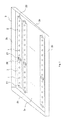
- a light source device As shown in Fig. 1 , a light source device according to this embodiment (hereinafter, referred to as the light source device simply) is configured in such a manner that a flat LED substrate 2 having LED elements 1 on its surface is mounted on a chassis 3.
- the LED element 1 is formed in such a manner that one or more (such as tow to four) LED chips (semiconductor bare chips) are connected in series and sealed in a translucent package, and composed of a pair of an anode terminal and a cathode terminal.
- the LED substrate 2 includes wiring metal thin films 21 (21 ⁇ 1> to 21 ⁇ 7>) and 22 provided on a surface side of a strip-shaped insulation substrate 20, and one radiating metal thin film 23 provided on a back surface side thereof, and solder resists 24 and 25 serving as insulation films to cover the wiring metal thin films 21 and 22 and the radiating metal thin film 23 are provided on both surfaces of the substrate 2.
- Fig. 2A is a plan view on the surface side of the LED substrate 2, in which the LED element 1 and the solder resist 24 are not shown.
- Fig. 2B is a plan view on the back surface side of the LED substrate 2, in which the solder resist 25 is not shown.
- FIG. 2C is a plan view on the surface side of the LED substrate 2 provided with the LED elements 1, in which the solder resist 24 is not shown.
- Fig. 3 is a cross-sectional view schematically showing an essential part of the LED substrate 2, in which the LED element 1 is connected to the LED substrate 2.
- the LED element 1 corresponds to a "light emitting element”
- the LED substrate 2 corresponds to a "substrate”
- the wiring metal thin films 21 and 22 correspond to a "first conductive thin film”
- the radiating metal thin film 23 corresponds to a "second conductive thin film”.
- the insulation substrate 20 is formed of woven or unwoven glass fiber or organic fiber impregnated with a resin (such as epoxy resin or cyanate resin).
- the wiring metal thin films 21 and 22 and the radiating metal thin film 23 are metal thin films composed of copper or the like, and may be plated with gold on their top surfaces according to need.
- the insulation substrate 20 has a plurality of through holes 26 (seven in Fig. 1 ) through which the LED substrate 2 is secured to the chassis 3 with screws or rivets.
- Each of the wiring metal thin films 21 and 22, the radiating metal thin film 23, and the solder resists 24 and 25 is formed so as not to overlap with the through hole 26 and its vicinity.
- an opening part is formed in the wiring metal thin film 21 and the solder resist 24, and it is used when an optical lens to diffuse emitted light of the LED element 1 in a lateral direction (parallel to the substrate surface) is bonded and fixed to the insulation substrate 20 although it is not shown.
- the wiring metal thin films 21 ⁇ 2> to 21 ⁇ 6> are provided with land parts 21a and 21b electrically connected to the anode terminal and the cathode terminal of the LED element 1
- the wiring metal thin film 21 ⁇ 1> is provided with the land part 21a electrically connected to the anode terminal of the LED element 1
- the wiring metal thin film 21 ⁇ 7> is provided with the land part 21b electrically connected to the cathode terminal of the LED element 1.
- the solder resists 24 on the surface side has opening parts to expose the land parts 21a and 21b, and is formed so as to cover a wiring part 21c other than the land parts 21a and 21b.
- the one land part 21a and the other land part 21b of the adjacent wiring metal thin films 21 are closely provided, and the anode terminal is connected to the cathode terminal in the one LED element 1, so that the six LED elements 1 are connected in series between the wiring metal thin film 21 ⁇ 1> and 21 ⁇ 7>.
- the number of the LED elements 1 mounted on the LED substrate 2 is not limited to six.
- the number of the wiring metal thin films 21 is determined according to the number of the LED elements 1.
- the wiring metal thin film 22 extends in a longitudinal direction of the LED substrate 2, and it is not used for electrically connecting the LED elements 1 mounted on the same substrate but used for connecting one end to the other end of the LED substrates 2. While the solder resist 25 covers the radiating metal thin film 23 on the back surface side, it does not necessarily have to insulate between the radiating metal thin film 23 and the chassis 3 because the radiating metal thin film 23 is set at the same potential as that of the chassis 3 and does not serve as the wiring film as will be described below.
- the radiating metal thin film 23 is provided so as to almost completely cover the back surface of the insulation substrate 20, on the back surface side of the LED substrate 2.
- the wiring part 21c of the wiring metal thin film 21 is also patterned so as to cover the surface of the insulation substrate 20 to a maximum extent.
- Two-terminal connectors 27 and 28 are provided at longitudinal both ends of the LED substrate 2, and one is a male connector and the other is a female connector.
- One terminal of the connector 27 is connected to the wiring metal thin film 21 ⁇ 1>, and the other thereof is connected to one end of the wiring metal thin film 22, and one terminal of the connector 28 is connected to the wiring metal thin film 21 ⁇ 7>, and the other thereof is connected to the other end of the wiring metal thin film 22.
- the plurality of LED substrates 2 arranged in the longitudinal direction of the LED substrate 2 are connected by connecting the one connector 28 sequentially to the other connector 27 between the two adjacent LED substrates 2 and the two terminals of the last connector 28 are short-circuited.
- a series circuit is formed of all of the LED elements 1 mounted on the sequentially connected LED substrates 2 between the two terminals of the head connector 27. Therefore, the one terminal of the head connector 27 serves as the anode terminal of the series circuit of the LED elements 1, and the other serves as the cathode terminal thereof.
- the number of the LED elements 1 in each of the sequentially connected LED substrate 2 is not necessarily the same, and when the LED substrates 2 having different number of LED elements 1 are combined, the series number of the series circuit of the LED elements 1 can be adjusted. As schematically shown in Fig.
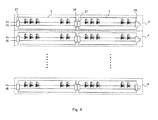
- the plurality of LED substrates 2 are arranged in the longitudinal direction of the LED substrate 2 and in its perpendicular direction in the form of an array, and the LED substrates 2 arranged in the longitudinal direction are connected as described above, whereby the series circuits 4 of the LED elements 1 are arranged in parallel.
- the chassis 3 is a metal chassis in the form of a flat box to house the LED substrates 2, and composed of a rectangular back surface plate 3a and four side plates 3b connected to its four sides, and its front surface is open.
- the light source device can be used as a backlight device for a liquid crystal display or an illuminating device.
- the back surface plate 3a of the chassis 3 corresponds to a "flat plate surface”.
- the chassis 3 is fixed to the ground potential in this embodiment.
- This method includes various methods because it only has to make the potential of the radiating metal thin film 23 conform to the potential of the back surface plate 3a.
- one end of a lead is connected to the radiating metal thin film 23 by soldering, and the other end is connected to the chassis 3.
- one part (such as a part around the through hole 26 provided in the insulation substrate 20 on the back surface side) of the solder resist 25 covering the radiating metal thin film 23 is largely opened, or without forming the solder resist 25 all over, the LED substrate 2 is secured to the back surface plate 3a with a screw or rivet so that the radiating metal thin film 23 is directly in contact with the back surface plate 3a.
- a projection part projecting toward the radiating metal thin film 23, on the back surface plate 3a so that the radiating metal thin film 23 can be easily in contact with the back surface plate 3a.
- a conductive tape such as an aluminum tape is attached on the solder resist 25, and it is partially pressed with a center punch and the like to penetrate the solder resist 25 to be in contact with the radiating metal thin film 23, and then the LED substrate 2 is secured to the back surface plate 3a with the screw or rivet so that the conductive tape is directly in contact with the back surface plate 3a.
- the third method it is preferable to provide a projection part projecting toward the radiating metal thin film 23, on the back surface plate 3a to be in contact with the conductive tape so that the conductive tape can be easily in contact with the back surface plate 3a.
- the projection part of the back surface plate 3a in the second and third methods may be formed by attaching the conductive tape such as the aluminum tape on the back surface plate 3a.
- three-terminal connectors 27 and 28 are provided at longitudinal both ends of the LED substrate 2, and one terminal of each connector is connected to the radiating metal thin film 23, so that the terminal of the connector 27 connected to the radiating metal thin film 23 has the same potential as that of the back surface plate 3a.
- the method to make the potential of the radiating metal thin film 23 conform to that of the back surface plate 3a is not limited to the above first to fourth methods.
- Figs. 5A and 5B are cross-sectional views schematically showing a positional relationship and a cross-sectional structure of each of the LED substrate 2 and the chassis 3.
- Fig. 5A shows a case where the radiating metal thin film 23 is in a floating state
- Fig. 5B shows a case where the potential of the radiating metal thin film 23 is at the same potential as that of the back surface plate 3a. Since the insulation substrate 20 is interposed between the wiring metal thin film 21 on the surface side and the radiating metal thin film 23 on the back surface side, it functions as a capacitor between the wiring metal thin film 21 and the radiating metal thin film 23.
- the potential of the wiring metal thin film 21 shown in Figs. 5A and 5B is a potential of one node on the series circuit 4 of the LED elements 1 shown in Fig. 4 .
- Fig. 6 shows one example of a drive circuit of the series circuit 4 of the LED elements 1 shown in Fig. 4 . As shown in Fig.
- the circuit is provided outside the light source device and composed of a AC/DC converter 5 to convert a AC power to a DC power and supply the converted power to each anode terminal 4a of the series circuit 4, and a control circuit 6 connected to each cathode terminal 4b of the series circuit 4, to control brightness of each LED element by driving a current flowing in each series circuit 4 by PWM (pulse width modulation), and controlling an effective current amount flowing in the LED element 1 of the series circuit 4.
- PWM pulse width modulation
- the LED element 1 is composed of three LED chips connected in series
- Vf forward bias
- the voltage drop between both ends of the LED element 1 is about 3 V due to intermittent on/off drive by the PWM.
- one series circuit 4 is composed of 13 LED elements 1
- a potential change for 13 LED elements 1 appears in the wiring metal thin film 21 ⁇ 7> connected to the cathode terminal 4b of the series circuit 4 and the wiring metal thin film 22.
- a potential fluctuation within a range of about 3 V to about 39V appears in the wiring metal thin films 21 on the series circuit 4.
- a small current (such as 1 mA or less) flows in the series circuit 4 even at the time of off of the on/off drive, and roughly the same voltage as the forward bias Vf is applied to each LED element 1.
- the larger drive current (such as several 10 mA) than that at the time of off is allowed to flow. Therefore, although a complete off state in which a current does not flow at all is not provided at the time of off of the turn/off drive, in the following description (including the descriptions of Figs. 8 and 9 ), the change in conductive state (large or small of the current) by the intermittent drive is distinguished such that the large current state is an on state and the small current state is off state.
- the potential fluctuation of the wiring metal thin films 21 on the surface side of the LED substrate 2 is coupled to the radiating metal thin film 23 on the back surface side of the LED substrate 2, due to capacitive coupling between the wiring metal thin film 21 and the radiating metal thin film 23, and the potential of the radiating metal thin film 23 also fluctuates in synchronization with the intermittent on/off drive by the PWM.
- the LED substrate 2 is secured to the chassis 3 with the screw or the rivet, and likely to be bent.
- Figs, 7A and 7B show a voltage waveform provided, by observing, with a, synchroscope, a voltage change induced in the radiating metal thin film 23 on the back side of the LED substrate 2 provided under the condition that the LED substrate 2 capable of carrying five of the LED elements 1 each composed of the three LED chips connected in series and the LED substrate 2 capable of carrying eight of them are connected in series to prepare test substrates in which a short circuit is caused between the adjacent land parts 21a and. 21b without carrying the LED element 1, and voltage pulses having the same voltage amplitude are commonly applied to the wiring metal thin films 21 and 22 on the surface side of the LED substrate 2, whereby the state in which the LED element 1 is mounted and driven by the PWM is simulated.
- Fig. 7A shows the case where the radiating metal thin film 23 is in the floating state
- Fig. 7B shows the case where the potential of the radiating metal thin film 23 is the same as that of the back surface plate 3a.
- an upper part shows a voltage waveform A applied to the wiring metal thin films 21 and 22, and a lower part shows a voltage waveform B induced in the radiating metal thin film 23.
- the voltage pulse applied to the wiring metal thin films 21 and 22 a frequency is 480 Hz, a duty ratio is 50%, and a voltage amplification is 45 V
- the voltage waveform B induced in the radiating metal thin film 23 is a differentiated waveform of the voltage waveform A, and changed within a range of about 4 V to + 4 V.
- the voltage waveforms shown in Fig. 7A and 7B are observed under the condition that the LED substrate 2 is supported by the chassis 3, and at the same time, subjective assessment is conducted regarding whether the noise (sound) is generated or not.
- the radiating metal thin film 23 is in the floating state shown in Fig. 7A , the sound is generated, and when the radiating metal thin film 23 has the same potential as that of the back surface plate 3a shown in Fig. 7B , the sound is not generated.
- the voltage change induced in the radiating metal thin film 23 is related to the sound, and the sound can be eliminated by suppressing the voltage change induced in the radiating metal thin film 23.
- the 13 LED elements 1 are distinguished as LED 1 to LED 13 in this order from the side close to the anode terminal of the series circuit.
- the five LED elements 1 on the side close to the anode terminal are mounted on a first LED substrate 2A
- the eight LED elements 1 apart from the anode terminal are mounted on a second LED substrate 2B
- Fig. 10 shows the voltage changes induced in the radiating metal thin films 23 on the back surface side of the first and second LED substrates 2A and 2B.
- the sound phenomenon can be moat effectively suppressed when the radiating metal thin film 23 of the LED substrate 2 whose voltage change induced in the radiating metal thin film 23 is largest is set to the same potential as that of the back surface plate 3a of the chassis 3.
- the circuit is configured such that the predetermined DC voltage is supplied from the power supply (AC/DC converter 5) to each anode terminal 4a of the series circuit 4, and the control circuit 6 is connected to each cathode terminal 4b of the series circuit 4, and the current flowing in each series circuit 4 is driven by the PWM.
- a circuit may be configured such that a predetermined DC voltage (such as the ground voltage) is supplied to each cathode terminal 4b of the series circuit 4, and the control circuit 6 to which a voltage is supplied from the power supply (AC/DC converter 5) is connected to each anode terminal 4a of the series circuit 4, and the current Sowing in each series circuit 4 is driven by the PWM.
- a predetermined DC voltage such as the ground voltage
- the drive of the series circuit 4 of the LED elements 1 is not necessarily limited to the PWM drive.
- the driven current since the driven current is turned on and off intermittently, the potential largely changes in each part of the wiring metal thin films 21 and 22 on the surface side of the LED substrate 2, so that the sound phenomenon becomes noticeable.
- the potential of the radiating metal thin film 23 on the back surface side of the LED substrate 2 is to be made to conform to that of the back surface plate 3a of the chassis 3 (or have a predetermined potential difference as will be described below).
- PDM pulse density modulation
- the above sound can be also suppressed when the potential of the radiating metal thin film 23 is constant and a potential difference from the potential of the back surface plate 3a of the chassis 3 is constant, similar to the case where the potential of the radiating metal thin film 23 is made to conform to that of the back surface plate 3a, because coulombic force applied between the radiating metal thin film 23 and the back surface plate 3a does not change in response to the on/off of the current to drive the LED element 1.
- the wiring metal thin film 22 on the surface side of the LED substrate 2 is provided on the back surface side, and the wiring metal thin film 22 is connected to the anode terminal 4a of the series circuit 4 of the LED elements 1, and the anode terminal and the cathode terminal of the LED element 1 connected to the wiring metal thin film 21 on the surface side are reversed, whereby a constant potential is supplied to the wiring metal thin film 22 on the back surface side
- the circuit may be configured such that each anode terminal 4a of the series circuit 4 is connected to the control circuit 6 and the current flowing in each series circuit 4 is driven by the PWM, and the wiring metal thin film 22 on the back surface side is connected to the cathode terminal 4b of the series circuit 4, whereby a constant potential
- the LED element is provided as the light emitting element in the above embodiments, the present invention is not limited to the LED element and any element may be used as long as it can emit light by a. current.
Landscapes
- Physics & Mathematics (AREA)
- Engineering & Computer Science (AREA)
- Nonlinear Science (AREA)
- General Physics & Mathematics (AREA)
- Theoretical Computer Science (AREA)
- Chemical & Material Sciences (AREA)
- Crystallography & Structural Chemistry (AREA)
- Computer Hardware Design (AREA)
- Optics & Photonics (AREA)
- Mathematical Physics (AREA)
- Planar Illumination Modules (AREA)
- Liquid Crystal (AREA)
- Fastening Of Light Sources Or Lamp Holders (AREA)
- Led Device Packages (AREA)
- Arrangement Of Elements, Cooling, Sealing, Or The Like Of Lighting Devices (AREA)
- Circuit Arrangement For Electric Light Sources In General (AREA)
- Led Devices (AREA)
- Non-Portable Lighting Devices Or Systems Thereof (AREA)
Abstract
Description
- The present invention relates to a light source device in which one or more flat substrates provided with a light emitting element on its surface side are supported by a chassis provided with a conductive flat plate surface in such a matter that a back surface of the substrate is opposed to the flat plate surface, and more particularly to a light source device which can be used as a backlight device of a transmissive liquid crystal display or an illuminating device.
- A transmissive liquid crystal display is provided with the backlight device as a light source on a back surface of a liquid crystal panel. Conventionally, while a CCFL (Cold Cathode Fluorescent Lamp) has predominated as the light source of the light source device used as the backlight, an LED (Light Emitting Diode) is expected to be used as the light source instead of the CCFL because a technology of the LED has been developed. For example, Japanese Unexamined Patent Application Publication No.
2003-207780 Document 1, a light source device can implement surface irradiation over a whole screen by diffusing the desired number of LED elements uniformly on a substrate. In addition, the surface irradiation can be implemented by arranging a plurality LED modules of a linear light source in which the plurality of LED elements are linearly arranged on a substrate, as disclosed in Japanese Unexamined Patent Application Publication No.2008-53062 Document 1, and a method for arranging a predetermined number of LED elements in series as disclosed in Japanese Examined Utility Model Application Publication No.62-34468 - Therefore, the LED module in which the plurality of LED elements are linearly arranged on a substrate and connected in series is provided with an
anode terminal 40 and acathode terminal 41 in the vicinity of an end side of aninsulation substrate 20, to draw out anodes and cathodes at both ends of the plurality ofLED elements 1 connected in series as schematically shown inFigs. 11A and 11B . According to the case shown inFigs. 11A and 11B , theanode terminal 40 and thecathode terminal 41 are adjacently arranged on one end of asubstrate 2.Figs. 11A and 11B show anLED module 50 in which eight LED elements are connected in series, as one example. Here,Fig. 11A shows a state before theLED elements 1 are mounted, andFig. 11B shows a state after theLED elements 1 have been mounted. - In the
LED module 50, nine connectingwires 31 to 39 to connect the eightLED elements 1 in series are formed on theinsulation substrate 20, and the connectingwires 31 to 39 are apart from each other and their ends are adjacently and sequentially arranged. One end of the first connectingwire 31 is connected to theanode terminal 40, and the other end is connected to anelectrode 42 connected to an anode of theLED element 1. Each one end of the second to eighth connectingwires 32 to 38 is connected to theelectrode 43 connected to the cathode of theLED element 1, and each other end thereof is connected to anelectrode 42 connected to an anode of theLED element 1. One end of the ninth connectingwire 39 is connected to thecathode terminal 41 and the other end is connected to theelectrode 43 connected to the cathode of theLED element 1. Thus, by connecting the anode and cathode of the LED element to theelectrodes LED elements 1 are forwardly connected in series between theanode terminal 40 and thecathode terminal 41. -
Figs. 12 and13 are configuration views of an LED light source device in which theLED modules 50 shown inFigs. 11A and 11B are arranged by 2 x 4 in the form of a matrix and the LEDs are arranged on a plane surface. For example, as shown inFig. 12 , according to a configuration in which theLED modules 50 are arranged in parallel, acontrol substrate 51 to drive the LED elements of eachLED module 50 and to control its emitted light is provided outside, and theanode terminal 40 and thecathode terminal 41 of eachLED module 50 are connected to thecontrol substrate 51 through anexternal wire 52. Furthermore, as shown inFig. 13 , according to a configuration in which four groups each composed of the twoLED modules 50 connected in series are arranged in parallel, the oneanode terminal 40 is connected to theother cathode terminal 41 between the twoadjacent LED modules 50, and theother anode terminal 40 and theother cathode terminal 41 are connected to thecontrol substrate 51 through theexternal wire 52. In either configuration, the light emission of eachLED module 50 can be controlled by thecontrol substrate 51. In addition, regarding the configuration shown inFig. 13 , since theLED modules 50 are connected in series, the number of terminals required for controlling thecontrol substrate 51 can be reduced. - Recently, the televisions are required to be reduced in thickness and weight. The reduction in weight can be implemented by reducing the number of components and reducing the size of the component in general. As a result, the substrate of the LED backlight is also reduced in area and in weight by arranging the strip-shaped substrates in the form of the array as shown in
Fig. 12 instead of spreading the LED elements all over the surface in the form of an array, whereby the weight reduction is implemented. Furthermore, the substrate is reduced in weight by reducing a thickness. - In addition, a simple method is employed in fixing the LED substrate with a view to reducing labor cost and because the LED substrate is reduced in size and weight. For example, instead of fixing the LED substrate with screws over the whole surface, a simple method such that both ends of the strip-shaped substrate are fixed with rivets (allowance is provided as compared with the fixing with screws) is used to implement inexpensive production.
- Furthermore, as for the reduction in thickness, it is required to reduce a distance from the chassis of the backlight device to a liquid crystal panel surface in the market. As a result, a gap between the chassis of the backlight device and the LED substrate is considerably narrowed.
- Because of the above reduction in weight, the LED substrate could be displaced even with small force. As a matter of course, since the LED substrate is fixed to the chassis, it is not largely moved, but the LED substrate could be slightly moved with small force because the substrate itself is bent due to reduction in thickness to reduce its weight, and there is an allowance gap of the small rivet.
- The inventor of this application has confirmed that the LED backlight device generates a noise (sound) under the above circumstances. Some level of sound reaches as high as 30 dB although depending on the size of the backlight device (corresponding liquid panel screen size), which negatively affects the viewing and listening of the television serving as audio visual (AV) equipment. Further examination has found that this sound phenomenon is generated due to contact between the LED substrate and the chassis provided on its back surface.
- By the way, when the LED elements are connected in series on the LED substrate, the same current flows in the LED elements, so that an essentially great benefit is that brightness of the LED element is uniform. Meanwhile, when the LED elements are connected in parallel, the problem is that the brightness of the LED element is not uniform unless the LED elements are driven separately. In addition, when the LED elements are driven separately, a wire for driving each LED element is needed, and the number of terminals of the drive circuit is increased, which is a problem for the LED substrate having the many LED elements. Therefore, the above problem is solved by connecting the LED elements in series.
- However, when the LED elements are connected in series, a drive voltage of the LED elements becomes high, so that a potential fluctuation of the LED substrate due to the on/off of the LED element also becomes large, which has been turned out to cause the sound to become conspicuous.
- The present invention has been made to solve the above problem of the sound phenomenon of the backlight device, and it is an object of the present invention to provide a light source device which can be used as the backlight device and does not generate sound.
- In order to achieve the above object, the present invention provides a light source device comprising one or more flat substrates each having a light emitting element on its surface side, the substrates being supported by a chassis having a conductive flat plate surface so that back surfaces of the substrates are opposed to the flat plate surface of the chassis, wherein each of the substrates is provided with a plurality of first conductive thin films for wiring formed on a surface side of an insulation substrate, and one or more second conductive thin films for radiating or wiring formed on a back surface side of the insulation substrate, two terminals of the light emitting element are connected to the two adjacent first conductive thin films, respectively and a potential of at least one of the second conductive thin films is fixed to have a constant potential difference with respect to a potential of the flat plate surface of the chassis.
- Furthermore, as for the light source device having the above characteristics, it is more preferable that the potential of at least one of the second conductive thin films is fixed to the same potential as the potential of the flat plate surface of the chassis.
- According to the light source device having the above characteristics, since a voltage applied to a capacitor formed of parallel flat plates composed of the second conductive thin films on the back surface side of the substrates and the flat plate surface of the chassis is constant or zero, the coulombic force induced between the parallel flat plates is constant and does not change, so that a change in distance between the parallel flat plates due to fluctuation in coulombic force is suppressed, and the sound due to the oscillation or contact of the parallel flat plates can be suppressed. Especially, when the potential of the second conductive thin films on the back surface side of the substrates is made to conform to that of the flat plate surface of the chassis, the coulombic force becomes zero, so that the sound due to the disposition of the parallel flat plates can be completely eliminated.
- Furthermore, as for the light source device having the above characteristics, it is preferable that at last one of the second conductive thin films is a radiating conductive thin film, and not electrically connected to the terminals of the light emitting element.
- Thus, when the second conductive thin films on the back surface side of the substrates are electrically isolated from the first conductive thin films on the surface side, the potential of the second conductive thin films can be optionally set, so that it can be easily made to conform to that of the flat plate surface of the chassis, and the sound phenomenon can be easily and surely suppressed.
- Furthermore, as for the light source device having the above characteristics, it is preferable that the plurality of light emitting elements are mounted on the one or more substrates, and at least two of the plurality of light emitting elements are connected in series to form a series circuit, and brightness of the plurality of light emitting elements of the series circuit is controlled by supplying a fixed potential from one side end of the series circuit and driving a current flowing in the series circuit from the other side end of the series circuit.
- Furthermore, as for the light source device having the above characteristics, it is preferable that a connection terminal is provided at an end side of each of the substrates or in a vicinity of the end side, electrically connected to the first conductive thin film formed in the vicinity of the end side, and used to electrically connect to an external circuit or another substrate, in which a series circuit is formed of the light emitting elements mounted on the plurality of substrates by connecting the connection terminal of one substrate to the connection terminal of another substrate to connect the plurality of substrates, and brightness of the plurality of light emitting elements of the series circuit is controlled by supplying a fixed potential from one side end of the series circuit and driving a current flowing in the series circuit from the other side end of the series circuit.
- Thus, when the series circuit of the light emitting elements is formed to control the brightness of the light emitting elements, the brightness of the plurality of light emitting elements can be uniformly controlled with the small number of control circuits. However, the amount of displacement between the parallel flat plates increases when the coulombic force fluctuates because the drive voltage becomes high, and the sound is generated conspicuously. However, since the voltage applied to the parallel flat plates is constant or zero, it is prevented that the sound is generated conspicuously because the plurality of light emitting elements are connected in series. Therefore, the present invention is especially effective in the configuration in which the plurality of light emitting elements are connected in series.
- Furthermore, as for the light source device having the above characteristics, it is preferable that a potential of the second conductive thin films is fixed to have a predetermined potential difference with respect to the potential of the flat plate surface of the chassis in at least one of the substrates, provided with the light emitting element having a maximum potential fluctuation at a terminal of the light emitting element due to the drive of the current flowing in the series circuit.
- Thus, without needing to make the second conductive thin films on the back surface side of the substrates have a constant potential difference from or be the same as that of the flat plate surface of the chassis with respect to each substrate, the sound can be effectively suppressed when the above is performed in only the specific substrate whose potential fluctuation in the second conductive thin films is great due to the capacitive coupling with the potential fluctuation of the first conductive thin films.
- Furthermore, as for the light source device having the above characteristics, it is preferable that the current flowing in the series circuit is driven by pulse width modulation.
- When the current flowing in the light emitting element is driven by the pulse width modulation, the potential fluctuation induced in the second conductive thin films increases and the coulombic force fluctuates because the current is driven intermittently, so that the displacement amount of the parallel flat plates increases. As a result, the sound is generated conspicuously. However, since the voltage applied between the parallel flat plates becomes constant or zero, it is prevented that the sound is generated conspicuously because the plurality of light emitting elements are connected in series. Therefore, the present invention is especially effective in the configuration in which the plurality of light emitting elements are connected in series and driven by the pulse width modulation.
- Furthermore, as for the light source device having the above characteristics, it is preferable that the potential of the second conductive thin films is fixed to the same potential as the potential of the flat plate surface of the chassis, by a conductive member to mount the substrates on the chassis.
- Furthermore, as for the light source device having the above characteristics, it is preferable that the potential of the second conductive thin films is fixed to the same potential as the potential of the flat plate surface of the chassis by opening a part of an insulation film covering the second conductive thin films provided on the back surface side of the substrates, and bringing the second conductive thin films exposed from the opening part of the insulation film into contact with the flat plate surface of the chassis directly or through a conductive connection member.
- Furthermore, as for the light source device having the above characteristics, it is preferable that a second connection terminal is provided at an end side of each of the substrates or in a vicinity of the end side, electrically connected to the second conductive thin films formed in the vicinity of the end side, and used to electrically connect to an external circuit or another substrate, in which the potential of the second conductive thin films is fixed to the same potential as the potential of the flat plate surface of the chassis by electrically connecting the second connection terminal to the flat plate surface of the chassis.
- According to the three kinds of light source devices described above, the second conductive thin films and the flat plate surface of the chassis can be easily set to be the same potential, and the sound can be simply and easily suppressed.
-
-
Fig. 1 is a perspective view schematically showing a configuration of a light source device according to one embodiment of the present invention; -
Figs. 2A to 2C are a plan view schematically showing a configuration on a surface side of an LED substrate before LED elements are mounted, a plan view schematically showing a configuration on the surface side of the LED substrate after the LED elements are mounted, and a plan view schematically showing a configuration on a back surface side of the LED substrate; -
Fig. 3 is a cross-sectional view schematically showing an essential part after the LED elements are mounted on the LED substrate; -
Fig. 4 is a view schematically showing a connection example in which the plurality of LED substrates are arranged in the form of an array; -
Figs. 5A and 5B are cross-sectional views schematically showing a positional relationship and a cross-sectional structure of each part of the LED substrate and a chassis; -
Fig. 6 is a block diagram showing one configuration example of a drive circuit of a series circuit of the LED elements shown inFig. 4 ; -
Figs. 7A and 7B are voltage waveform diagrams showing a verification experiment result of a mechanism of generating a sound phenomenon; -
Fig. 8 is a list of voltage data showing a voltage change generated in a cathode terminal of each LED element of a series circuit composed of 13 LED elements; -
Fig. 9 is a graph of the voltage data shown inFig. 8 ; -
Fig. 10 is a voltage waveform diagram showing a voltage change induced in each radiating metal thin film on the back surface side of the LED substrate due to the voltage change shown inFigs. 7A and 7B ; -
Figs. 11A and 11B are plan views schematically showing one configuration example of a conventional LED module; -
Fig. 12 is a view showing a connection example in which eight LED modules shown inFigs. 11A and 11B are connected in parallel; and -
Fig. 13 is a view showing a connection example in which eight LED modules shown inFigs. 11A and 11B are connected in parallel. - An embodiment of a light source device according to the present invention will be described with reference to the drawings. In addition, in the following drawings, a main part is emphasized and a dimension ratio of each part does not coincide with an actual dimension ratio, in order to easily understand the description.
- As shown in
Fig. 1 , a light source device according to this embodiment (hereinafter, referred to as the light source device simply) is configured in such a manner that aflat LED substrate 2 havingLED elements 1 on its surface is mounted on achassis 3. - The
LED element 1 is formed in such a manner that one or more (such as tow to four) LED chips (semiconductor bare chips) are connected in series and sealed in a translucent package, and composed of a pair of an anode terminal and a cathode terminal. - As schematically shown in
Figs. 2A to 2C andFig. 3 , theLED substrate 2 includes wiring metal thin films 21 (21 <1> to 21 <7>) and 22 provided on a surface side of a strip-shapedinsulation substrate 20, and one radiating metalthin film 23 provided on a back surface side thereof, and solder resists 24 and 25 serving as insulation films to cover the wiring metalthin films thin film 23 are provided on both surfaces of thesubstrate 2.Fig. 2A is a plan view on the surface side of theLED substrate 2, in which theLED element 1 and the solder resist 24 are not shown.Fig. 2B is a plan view on the back surface side of theLED substrate 2, in which the solder resist 25 is not shown.Fig. 2C is a plan view on the surface side of theLED substrate 2 provided with theLED elements 1, in which the solder resist 24 is not shown.Fig. 3 is a cross-sectional view schematically showing an essential part of theLED substrate 2, in which theLED element 1 is connected to theLED substrate 2. Here, theLED element 1 corresponds to a "light emitting element", theLED substrate 2 corresponds to a "substrate", the wiring metalthin films thin film 23 corresponds to a "second conductive thin film". - The
insulation substrate 20 is formed of woven or unwoven glass fiber or organic fiber impregnated with a resin (such as epoxy resin or cyanate resin). The wiring metalthin films thin film 23 are metal thin films composed of copper or the like, and may be plated with gold on their top surfaces according to need. Theinsulation substrate 20 has a plurality of through holes 26 (seven inFig. 1 ) through which theLED substrate 2 is secured to thechassis 3 with screws or rivets. Each of the wiring metalthin films thin film 23, and the solder resists 24 and 25 is formed so as not to overlap with the throughhole 26 and its vicinity. In addition, on the surface side of theLED substrate 2, an opening part is formed in the wiring metalthin film 21 and the solder resist 24, and it is used when an optical lens to diffuse emitted light of theLED element 1 in a lateral direction (parallel to the substrate surface) is bonded and fixed to theinsulation substrate 20 although it is not shown. - The wiring metal
thin films 21 <2> to 21 <6> are provided withland parts LED element 1, the wiring metalthin film 21 <1> is provided with theland part 21a electrically connected to the anode terminal of theLED element 1, and the wiring metalthin film 21 <7> is provided with theland part 21b electrically connected to the cathode terminal of theLED element 1. The solder resists 24 on the surface side has opening parts to expose theland parts wiring part 21c other than theland parts - The one
land part 21a and theother land part 21b of the adjacent wiring metalthin films 21 are closely provided, and the anode terminal is connected to the cathode terminal in the oneLED element 1, so that the sixLED elements 1 are connected in series between the wiring metalthin film 21 <1> and 21 <7>. Here, the number of theLED elements 1 mounted on theLED substrate 2 is not limited to six. In addition, the number of the wiring metalthin films 21 is determined according to the number of theLED elements 1. - The wiring metal
thin film 22 extends in a longitudinal direction of theLED substrate 2, and it is not used for electrically connecting theLED elements 1 mounted on the same substrate but used for connecting one end to the other end of theLED substrates 2. While the solder resist 25 covers the radiating metalthin film 23 on the back surface side, it does not necessarily have to insulate between the radiating metalthin film 23 and thechassis 3 because the radiating metalthin film 23 is set at the same potential as that of thechassis 3 and does not serve as the wiring film as will be described below. - In addition, in order to efficiently diffuse heat generated due to the light emission of the
LED element 1, the radiating metalthin film 23 is provided so as to almost completely cover the back surface of theinsulation substrate 20, on the back surface side of theLED substrate 2. In addition, thewiring part 21c of the wiring metalthin film 21 is also patterned so as to cover the surface of theinsulation substrate 20 to a maximum extent. - Two-
terminal connectors LED substrate 2, and one is a male connector and the other is a female connector. One terminal of theconnector 27 is connected to the wiring metalthin film 21 <1>, and the other thereof is connected to one end of the wiring metalthin film 22, and one terminal of theconnector 28 is connected to the wiring metalthin film 21 <7>, and the other thereof is connected to the other end of the wiring metalthin film 22. The plurality ofLED substrates 2 arranged in the longitudinal direction of theLED substrate 2 are connected by connecting the oneconnector 28 sequentially to theother connector 27 between the twoadjacent LED substrates 2 and the two terminals of thelast connector 28 are short-circuited. Thus, a series circuit is formed of all of theLED elements 1 mounted on the sequentiallyconnected LED substrates 2 between the two terminals of thehead connector 27. Therefore, the one terminal of thehead connector 27 serves as the anode terminal of the series circuit of theLED elements 1, and the other serves as the cathode terminal thereof. The number of theLED elements 1 in each of the sequentiallyconnected LED substrate 2 is not necessarily the same, and when theLED substrates 2 having different number ofLED elements 1 are combined, the series number of the series circuit of theLED elements 1 can be adjusted. As schematically shown inFig. 4 , the plurality ofLED substrates 2 are arranged in the longitudinal direction of theLED substrate 2 and in its perpendicular direction in the form of an array, and theLED substrates 2 arranged in the longitudinal direction are connected as described above, whereby theseries circuits 4 of theLED elements 1 are arranged in parallel. - The
chassis 3 is a metal chassis in the form of a flat box to house theLED substrates 2, and composed of a rectangularback surface plate 3a and fourside plates 3b connected to its four sides, and its front surface is open. When a diffuser plate or a translucent plate material is provided on the front surface, the light source device can be used as a backlight device for a liquid crystal display or an illuminating device. Here, theback surface plate 3a of thechassis 3 corresponds to a "flat plate surface". In addition, thechassis 3 is fixed to the ground potential in this embodiment. - Next, a description will be briefly made of a method for fixing the potential of the radiating metal
thin film 23 of theLED substrate 2 to the same potential as that of theback surface plate 3a of thechassis 3 in order to prevent a noise (sound) of the light source device which will be described below. - This method includes various methods because it only has to make the potential of the radiating metal
thin film 23 conform to the potential of theback surface plate 3a. For example, as a first method, one end of a lead is connected to the radiating metalthin film 23 by soldering, and the other end is connected to thechassis 3. As a second method, one part (such as a part around the throughhole 26 provided in theinsulation substrate 20 on the back surface side) of the solder resist 25 covering the radiating metalthin film 23 is largely opened, or without forming the solder resist 25 all over, theLED substrate 2 is secured to theback surface plate 3a with a screw or rivet so that the radiating metalthin film 23 is directly in contact with theback surface plate 3a. In addition, in the second method, it is preferable to provide a projection part projecting toward the radiating metalthin film 23, on theback surface plate 3a so that the radiating metalthin film 23 can be easily in contact with theback surface plate 3a. As a third method, a conductive tape such as an aluminum tape is attached on the solder resist 25, and it is partially pressed with a center punch and the like to penetrate the solder resist 25 to be in contact with the radiating metalthin film 23, and then theLED substrate 2 is secured to theback surface plate 3a with the screw or rivet so that the conductive tape is directly in contact with theback surface plate 3a. In addition, in the third method, it is preferable to provide a projection part projecting toward the radiating metalthin film 23, on theback surface plate 3a to be in contact with the conductive tape so that the conductive tape can be easily in contact with theback surface plate 3a. The projection part of theback surface plate 3a in the second and third methods may be formed by attaching the conductive tape such as the aluminum tape on theback surface plate 3a. As a fourth method, three-terminal connectors LED substrate 2, and one terminal of each connector is connected to the radiating metalthin film 23, so that the terminal of theconnector 27 connected to the radiating metalthin film 23 has the same potential as that of theback surface plate 3a. In addition, the method to make the potential of the radiating metalthin film 23 conform to that of theback surface plate 3a is not limited to the above first to fourth methods. - Next, a detailed description will be made of a mechanism of generating the noise (sound) of the light source device, and the reason why the sound is effectively suppressed by setting the potential of the radiating metal
thin film 23 to be the same potential as that of theback surface plate 3a, with reference to the drawings. -
Figs. 5A and 5B are cross-sectional views schematically showing a positional relationship and a cross-sectional structure of each of theLED substrate 2 and thechassis 3.Fig. 5A shows a case where the radiating metalthin film 23 is in a floating state, andFig. 5B shows a case where the potential of the radiating metalthin film 23 is at the same potential as that of theback surface plate 3a. Since theinsulation substrate 20 is interposed between the wiring metalthin film 21 on the surface side and the radiating metalthin film 23 on the back surface side, it functions as a capacitor between the wiring metalthin film 21 and the radiating metalthin film 23. - The potential of the wiring metal
thin film 21 shown inFigs. 5A and 5B is a potential of one node on theseries circuit 4 of theLED elements 1 shown inFig. 4 .Fig. 6 shows one example of a drive circuit of theseries circuit 4 of theLED elements 1 shown inFig. 4 . As shown inFig. 6 , the circuit is provided outside the light source device and composed of a AC/DC converter 5 to convert a AC power to a DC power and supply the converted power to each anode terminal 4a of theseries circuit 4, and acontrol circuit 6 connected to eachcathode terminal 4b of theseries circuit 4, to control brightness of each LED element by driving a current flowing in eachseries circuit 4 by PWM (pulse width modulation), and controlling an effective current amount flowing in theLED element 1 of theseries circuit 4. - In a case where the
LED element 1 is composed of three LED chips connected in series, when a drive current is applied to theseries circuit 4 to light up, voltage drop of about 11 V which exceeds forward bias Vf (about 8 V) of the three LED chips is generated in oneLED element 1. Therefore, the voltage drop between both ends of theLED element 1 is about 3 V due to intermittent on/off drive by the PWM. When it is assumed that oneseries circuit 4 is composed of 13LED elements 1, a potential change for 13 LED elements 1 (about 3 V x 13 = about 39 V) appears in the wiring metalthin film 21 <7> connected to thecathode terminal 4b of theseries circuit 4 and the wiring metalthin film 22. Therefore, a potential fluctuation within a range of about 3 V to about 39V appears in the wiring metalthin films 21 on theseries circuit 4. In addition, according to this embodiment, a small current (such as 1 mA or less) flows in theseries circuit 4 even at the time of off of the on/off drive, and roughly the same voltage as the forward bias Vf is applied to eachLED element 1. At the time of on, the larger drive current (such as several 10 mA) than that at the time of off is allowed to flow. Therefore, although a complete off state in which a current does not flow at all is not provided at the time of off of the turn/off drive, in the following description (including the descriptions ofFigs. 8 and9 ), the change in conductive state (large or small of the current) by the intermittent drive is distinguished such that the large current state is an on state and the small current state is off state. - As shown in
Fig. 5A , when the radiating metalthin film 23 is in the floating state, the potential fluctuation of the wiring metalthin films 21 on the surface side of theLED substrate 2 is coupled to the radiating metalthin film 23 on the back surface side of theLED substrate 2, due to capacitive coupling between the wiring metalthin film 21 and the radiating metalthin film 23, and the potential of the radiating metalthin film 23 also fluctuates in synchronization with the intermittent on/off drive by the PWM. Here, as described above, under the circumstances that the gap between thechassis 3 of the backlight device and theLED substrate 2 is very small, theLED substrate 2 is secured to thechassis 3 with the screw or the rivet, and likely to be bent. Thus, when the potential of the radiating metalthin film 23 opposed in parallel to theback surface plate 3a of thechassis 3 largely fluctuates with respect to the ground potential of thechassis 3, in synchronization with the PWM drive as described above, it is thought that coulombic force applied between theback surface plate 3a and the radiating metalthin film 23 changes, and a relative distance between theback surface plate 3a and the radiating metalthin film 23 fluctuates, so that the thinnedLED substrate 2 oscillates and comes into contact with theback surface plate 3a repeatedly, and the sound phenomenon is generated. In addition, when theLED substrate 2 oscillates, the above sound phenomenon could be generated due to friction with the other member such as a screw or rivet to support theLED substrate 2 even when it doe not come into contact with theback surface plate 3a repeatedly. - Meanwhile, as shown in
Fig. 5B , when the potential of the radiating metalthin film 23 is set to the same potential as that of theback surface plate 3a of thechassis 3, the potential fluctuation of the wiring metalthin film 21 on the surface side of theLED substrate 2 is prevented from appearing on the radiating metalthin film 23 on the back surface side of theLED substrate 2 due to the capacitive coupling, and the coulombic force itself is prevented from being applied between theback surface plate 3a and the radiating metalthin film 23, so that the sound phenomenon caused by the change in coulombic force can be prevented. - Next, a description will be made of a verification experiment of a mechanism of generating the sound phenomenon, and a result of an experiment to confirm a sound suppression effect.
-
Figs, 7A and 7B show a voltage waveform provided, by observing, with a, synchroscope, a voltage change induced in the radiating metalthin film 23 on the back side of theLED substrate 2 provided under the condition that theLED substrate 2 capable of carrying five of theLED elements 1 each composed of the three LED chips connected in series and theLED substrate 2 capable of carrying eight of them are connected in series to prepare test substrates in which a short circuit is caused between theadjacent land parts 21a and. 21b without carrying theLED element 1, and voltage pulses having the same voltage amplitude are commonly applied to the wiring metalthin films LED substrate 2, whereby the state in which theLED element 1 is mounted and driven by the PWM is simulated.Fig. 7A shows the case where the radiating metalthin film 23 is in the floating state, andFig. 7B shows the case where the potential of the radiating metalthin film 23 is the same as that of theback surface plate 3a. In either case, an upper part shows a voltage waveform A applied to the wiring metalthin films thin film 23. As for the voltage pulse applied to the wiring metalthin films thin film 23 is a differentiated waveform of the voltage waveform A, and changed within a range of about 4 V to + 4 V. - In addition, the voltage waveforms shown in
Fig. 7A and 7B are observed under the condition that theLED substrate 2 is supported by thechassis 3, and at the same time, subjective assessment is conducted regarding whether the noise (sound) is generated or not. As a result, when the radiating metalthin film 23 is in the floating state shown inFig. 7A , the sound is generated, and when the radiating metalthin film 23 has the same potential as that of theback surface plate 3a shown inFig. 7B , the sound is not generated. According to the above result, it has been confirmed that the voltage change induced in the radiating metalthin film 23 is related to the sound, and the sound can be eliminated by suppressing the voltage change induced in the radiating metalthin film 23. - Then, under the condition that the two kinds of
LED substrates 2 used in the voltage waveform observation shown inFigs, 7A and 7B are connected in series, and theLED elements 1. each composed of three LED chips connected in series are mounted, whereby a series circuit is formed of the 13LED elements 1, potential changes of the wiring metalthin films 21 connected to the cathode terminals of the 13LED elements 1 are observed at the time of on and off of theLED elements 1 when the series circuit is driven by the PWM. Its result is shown in a table inFig. 8 and in a graph inFig. 9 , and a voltage change induced in the radiating metalthin film 23 of each of the two kinds ofLED substrates 2 is shown inFig. 10 . In this experiment, 152.2 V is applied to the anode terminal of the series circuit of the 13LED elements 1, and a current of 60 mA is driven by the PWM at a frequency of 20 Hz and at a duty ratio of 50% from the cathode terminal of this series circuit. InFigs. 8 and9 , the 13LED elements 1 are distinguished asLED 1 to LED 13 in this order from the side close to the anode terminal of the series circuit. In addition, the fiveLED elements 1 on the side close to the anode terminal are mounted on a first LED substrate 2A, and the eightLED elements 1 apart from the anode terminal are mounted on a second LED substrate 2B, andFig. 10 shows the voltage changes induced in the radiating metalthin films 23 on the back surface side of the first and second LED substrates 2A and 2B. - As shown in
Figs. 8 and9 , since a constant voltage is applied to the anode terminal of the series circuit of the 13LED elements 1, and the current is driven from the side of the cathode terminal of the series circuit, the voltage changes of theLED elements 1 at the time of on and off increase with the increasing distance from the anode terminal. As a result, as shown inFig. 10 , of the two kinds ofLED substrates 2, the voltage change induced in the radiating metalthin film 23 of the second LED substrate 2B on the side distant from the anode terminal of the series circuit is larger than the voltage change induced in the radiating metalthin film 23 of the first LED substrate 2A on the side close to the anode terminal of the series circuit. This result coincides with the result of the subjective evaluation revealing that the sound generated due to the oscillations of the second LED substrate 2B is louder than that of the first LED substrate 2A. - Therefore, in the case where the plurality of
LED substrates 2 are connected in series, and the series circuit of theLED elements 1 is formed, and the potential of the radiating metalthin film 23 of any one of theLED substrate 2 among the plurality ofLED substrates 2 is made to conform to that of theback surface plate 3a of thechassis 3, the sound phenomenon can be moat effectively suppressed when the radiating metalthin film 23 of theLED substrate 2 whose voltage change induced in the radiating metalthin film 23 is largest is set to the same potential as that of theback surface plate 3a of thechassis 3. - Hereinafter, a description will be made of another embodiment of the device of the present invention.
- (1) According to the above embodiment, as one example of the drive circuit of the
series circuit 4 of theLED elements 1, as shown inFig. 6 , the circuit is configured such that the predetermined DC voltage is supplied from the power supply (AC/DC converter 5) to each anode terminal 4a of theseries circuit 4, and thecontrol circuit 6 is connected to eachcathode terminal 4b of theseries circuit 4, and the current flowing in eachseries circuit 4 is driven by the PWM. Here, instead of the above, a circuit may be configured such that a predetermined DC voltage (such as the ground voltage) is supplied to eachcathode terminal 4b of theseries circuit 4, and thecontrol circuit 6 to which a voltage is supplied from the power supply (AC/DC converter 5) is connected to each anode terminal 4a of theseries circuit 4, and the current Sowing in eachseries circuit 4 is driven by the PWM. - Furthermore, the drive of the
series circuit 4 of theLED elements 1 is not necessarily limited to the PWM drive. In the case of pulse drive, since the driven current is turned on and off intermittently, the potential largely changes in each part of the wiring metalthin films LED substrate 2, so that the sound phenomenon becomes noticeable. Thus, in another drive method also, when the similar sound phenomenon is generated, like the above embodiment, the potential of the radiating metalthin film 23 on the back surface side of theLED substrate 2 is to be made to conform to that of theback surface plate 3a of the chassis 3 (or have a predetermined potential difference as will be described below). - In addition, in a case where pulse density modulation (PDM) is used as the same pulse drive, while the sound phenomenon similar to the PWM drive is prominently generated, the sound phenomenon can be effectively prevented by the present invention.
- (2) While the potential of the radiating metal
thin film 23 on the back surface side of theLED substrate 2 is set to the same as that of theback surface plate 3a of thechassis 3 in the above embodiment in order to suppress the noise (sound) of the light source device, the above sound can be also suppressed when the potential of the radiating metalthin film 23 is constant and a potential difference from the potential of theback surface plate 3a of thechassis 3 is constant, similar to the case where the potential of the radiating metalthin film 23 is made to conform to that of theback surface plate 3a, because coulombic force applied between the radiating metalthin film 23 and theback surface plate 3a does not change in response to the on/off of the current to drive theLED element 1. - This fact means that it is only necessary to provide a wiring metal thin film instead of the radiating metal
thin film 23 or in addition to it, on the back surface side of theLED substrate 2 and use a drive method to keep constant the potential supplied to the wiring metal thin film. For example, the wiring metalthin film 22 on the surface side of theLED substrate 2 is provided on the back surface side, and the wiring metalthin film 22 is connected to the anode terminal 4a of theseries circuit 4 of theLED elements 1, and the anode terminal and the cathode terminal of theLED element 1 connected to the wiring metalthin film 21 on the surface side are reversed, whereby a constant potential is supplied to the wiring metalthin film 22 on the back surface side, Alternatively, as shown in the another embodiment (1), the circuit may be configured such that each anode terminal 4a of theseries circuit 4 is connected to thecontrol circuit 6 and the current flowing in eachseries circuit 4 is driven by the PWM, and the wiring metalthin film 22 on the back surface side is connected to thecathode terminal 4b of theseries circuit 4, whereby a constant potential is supplied to the wiring' metalthin film 22 on the back surface side. - (3) The material and shape of each part shown in the above embodiments are one example and the present invention is not limited to the above. In addition, while the
connectors LED substrate 2, an electrode (land) to solder an external wire (lead or the like) may be provided on theinsulation substrate 20 instead of theconnectors - (4) While the LED element is provided as the light emitting element in the above embodiments, the present invention is not limited to the LED element and any element may be used as long as it can emit light by a. current.
Claims (11)
- A light source device comprising
one or more flat substrates each having a light emitting element on its surface side, the substrates being supported by a chassis having a conductive flat plate surface so that back surfaces of the substrates are opposed to the flat plate surface of the chassis, wherein
each of the substrates is provided with a plurality of first conductive thin films for wiring formed on a surface side of an insulation substrate, and one or more second conductive thin films for radiating or wiring formed on a back surface side of the insulation substrate,
two terminals of the light emitting element, are connected to the two adjacent first conductive thin films, respectively and
a potential of at least one of the second conductive thin films is fixed to have a constant potential difference with respect to a potential of the flat plate surface of the chassis. - The light source device according to claim 1, wherein
the potential of at least one of the second conductive thin films is fixed to the same potential as the potential of the flat plate surface of the chassis. - The light source device according to claim 1 or 2, wherein
at last one of the second conductive thin films is a radiating conductive thin film, and not electrically connected to the terminals of the light emitting element. - The light source device according to claim 3, wherein
a potential of the radiating conductive thin film is fixed to the same potential as the potential of the flat plate surface of the chassis. - The light source device according to any one of claims 1 to 4, wherein
the plurality of light emitting elements are mounted on the one or more substrates, and at least two of the plurality of light emitting elements are connected in series to form a series circuit, and
brightness of the plurality of light emitting elements of the series circuit is controlled by supplying a fixed potential from one side end of the series circuit and driving a current flowing in the series circuit from the other side end of the series circuit. - The light source device according to any one of claims 1 to 4, comprising
a connection terminal at an end side of each of the substrates or in a vicinity of the end side, electrically connected to the first conductive thin film formed in the vicinity of the end side, and used to electrically connect to an external circuit or the other substrate, wherein
a series circuit is formed of the light emitting elements mounted on the plurality of substrates by connecting the connection terminal of the one substrate to the connection terminal of the other substrate to connect the plurality of substrates, and
brightness of the plurality of light emitting elements of the series circuit is controlled by supplying a fixed potential from one side end of the series circuit and driving a current flowing in the series circuit from the other side end of the series circuit. - The light source device according to claim 6, wherein
a potential of the second conductive thin films is fixed to have a predetermined potential difference with respect to the potential of the flat plate surface of the chassis in at least one of the plurality of substrates, provided with the light emitting element having a maximum potential fluctuation at a terminal of the light emitting element due to drive of the current flowing in the series circuit. - The light source device according to any one of claims 5 to 7, wherein
the current flowing in the series circuit is driven by pulse width modulation. - The light source device according to any one of claims 1 to 8, wherein
the potential of at least one of the second conductive thin films is fixed to the same potential as the potential of the flat plate surface of the chassis, by a conductive member to mount the substrates on the chassis. - The light source device according to any one of claims 1 to 8, wherein
the potential of at least one of the second conductive thin films is fixed to the same potential as the potential of the flat plate surface of the chassis by opening a part of an insulation film covering the second conductive thin films provided on the back surface side of the substrates, and bringing the second conductive thin film exposed from the opening part of the insulation film into contact with the flat plate surface of the chassis directly or through a conductive connection member. - The light source device according to any one of claims 1 to 8, comprising
a second connection terminal provided at an end side of each of the substrates or in a vicinity of the end side, electrically connected to the second conductive thin films formed in the vicinity of the end side, and used to electrically connect to an external circuit or the other substrate, wherein
the potential of at least one of the second conductive thin films is fixed to the same potential as the potential of the flat plate surface of the chassis by electrically connecting the second connection terminal to the flat plate surface of the chassis.
Applications Claiming Priority (1)
| Application Number | Priority Date | Filing Date | Title |
|---|---|---|---|
| JP2009197277A JP4910023B2 (en) | 2009-08-27 | 2009-08-27 | Light source device |
Publications (2)
| Publication Number | Publication Date |
|---|---|
| EP2293278A2 true EP2293278A2 (en) | 2011-03-09 |
| EP2293278A3 EP2293278A3 (en) | 2011-03-30 |
Family
ID=43242608
Family Applications (1)
| Application Number | Title | Priority Date | Filing Date |
|---|---|---|---|
| EP10172731A Withdrawn EP2293278A3 (en) | 2009-08-27 | 2010-08-13 | Light source device |
Country Status (6)
| Country | Link |
|---|---|
| US (1) | US8497638B2 (en) |
| EP (1) | EP2293278A3 (en) |
| JP (1) | JP4910023B2 (en) |
| KR (1) | KR101199126B1 (en) |
| CN (1) | CN102003640B (en) |
| TW (1) | TWI412698B (en) |
Families Citing this family (43)
| Publication number | Priority date | Publication date | Assignee | Title |
|---|---|---|---|---|
| KR20090015734A (en) * | 2007-08-09 | 2009-02-12 | 엘지이노텍 주식회사 | Light source device |
| WO2012002010A1 (en) * | 2010-06-28 | 2012-01-05 | パナソニック液晶ディスプレイ株式会社 | Liquid crystal display device and television receiver |
| WO2012128074A1 (en) * | 2011-03-18 | 2012-09-27 | シャープ株式会社 | Illumination device, display device, and television reception device |
| KR101257407B1 (en) * | 2011-04-08 | 2013-04-23 | 주식회사 알.에프.텍 | Led lighting apparatus |
| WO2013040453A2 (en) * | 2011-09-16 | 2013-03-21 | Air Motion Systems, Inc. | Assembly and interconnection method for high-power led devices |
| SG189603A1 (en) * | 2011-11-04 | 2013-05-31 | Opulent Electronics Internat Pte Ltd | System for driving a plurality of high powered led units |
| KR101282725B1 (en) * | 2011-11-10 | 2013-07-05 | 교우세라 커넥터 프로덕츠 가부시키가이샤 | Module for Mounting LED And LED Module |
| JP6035766B2 (en) * | 2012-02-15 | 2016-11-30 | 三菱電機株式会社 | LED lighting device |
| KR101992718B1 (en) * | 2012-04-24 | 2019-06-26 | 삼성전자주식회사 | Display apparatus |
| KR101390374B1 (en) * | 2012-05-14 | 2014-04-29 | 남경 주식회사 | Lighting equipment |
| KR101402650B1 (en) * | 2012-06-18 | 2014-06-03 | 교우세라 커넥터 프로덕츠 가부시키가이샤 | Module for mounting LED module and LED module having the same |
| CN102750911B (en) * | 2012-07-10 | 2015-11-25 | 深圳市华星光电技术有限公司 | A kind of LED backlight drive circuit, backlight module and liquid crystal indicator |
| JP5522643B2 (en) * | 2012-07-13 | 2014-06-18 | シャープ株式会社 | Light emitting device |
| JP5907388B2 (en) * | 2012-09-24 | 2016-04-26 | 東芝ライテック株式会社 | Light emitting device and lighting device |
| TWI481008B (en) * | 2012-11-22 | 2015-04-11 | 隆達電子股份有限公司 | Illuminating device |
| US9482410B2 (en) | 2012-12-11 | 2016-11-01 | Samsung Electronics Co., Ltd. | Light emitting module and surface lighting device having the same |
| KR101301719B1 (en) * | 2013-01-24 | 2013-09-10 | 주식회사 트루스타 | Electrode module for led lamp |
| JP6136501B2 (en) * | 2013-04-12 | 2017-05-31 | 船井電機株式会社 | Display device |
| JP2014230033A (en) * | 2013-05-21 | 2014-12-08 | 株式会社東芝 | Circuit and television apparatus |
| US9318360B2 (en) * | 2013-10-11 | 2016-04-19 | Applied Materials, Inc. | Linear high packing density for LED arrays |
| TWI601909B (en) * | 2014-02-11 | 2017-10-11 | 晶元光電股份有限公司 | Light emitting device and method of manufacturing same |
| US9653671B2 (en) | 2014-02-13 | 2017-05-16 | Infineon Technologies Ag | Light emitting device and method for operating a plurality of light emitting arrangements |
| JP5687784B1 (en) * | 2014-02-26 | 2015-03-18 | アイリスオーヤマ株式会社 | LED lighting device |
| CN103956359A (en) * | 2014-05-19 | 2014-07-30 | 四川柏狮光电技术有限公司 | Single-ended power supply all-around LED lamp filament and manufacturing method thereof |
| EP3318109B1 (en) * | 2015-07-02 | 2026-04-01 | Lumileds LLC | An led lighting device |
| WO2017038080A1 (en) * | 2015-09-01 | 2017-03-09 | パナソニックIpマネジメント株式会社 | Video display device |
| WO2017038083A1 (en) | 2015-09-01 | 2017-03-09 | パナソニックIpマネジメント株式会社 | Image display device |
| EP3346322B1 (en) | 2015-09-01 | 2020-09-30 | Panasonic Intellectual Property Management Co., Ltd. | Video display device |
| WO2017038085A1 (en) | 2015-09-01 | 2017-03-09 | パナソニックIpマネジメント株式会社 | Image display device |
| JP6688956B2 (en) | 2015-09-01 | 2020-04-28 | パナソニックIpマネジメント株式会社 | Video display |
| WO2017038084A1 (en) | 2015-09-01 | 2017-03-09 | パナソニックIpマネジメント株式会社 | Video display device |
| CN105627122B (en) * | 2016-03-30 | 2018-11-27 | 湖南粤港模科实业有限公司 | It is a kind of directly using metal heat sink as the LED light source module of positive and negative electrode circuit |
| JP6384565B2 (en) * | 2017-04-25 | 2018-09-05 | 船井電機株式会社 | Display device |
| JP2019025009A (en) * | 2017-07-31 | 2019-02-21 | 株式会社大一商会 | Game machine |
| JP2019025010A (en) * | 2017-07-31 | 2019-02-21 | 株式会社大一商会 | Game machine |
| JP2019080688A (en) * | 2017-10-30 | 2019-05-30 | 株式会社大一商会 | Game machine |
| JP2019197610A (en) * | 2018-05-07 | 2019-11-14 | 株式会社小糸製作所 | Luminaire |
| JP7085264B2 (en) * | 2018-08-08 | 2022-06-16 | 株式会社大一商会 | Pachinko machine |
| CN111290171B (en) * | 2020-02-18 | 2023-04-11 | 京东方科技集团股份有限公司 | Direct type backlight source, backlight module and display device |
| US11442312B2 (en) * | 2020-05-22 | 2022-09-13 | Apple Inc. | Electronic device display with a backlight having light-emitting diodes and driver integrated circuits in an active area |
| CN112130373B (en) * | 2020-08-25 | 2025-06-13 | 厦门厦华科技有限公司 | Light bar circuit, direct-type backlight module and display device |
| CN114779531B (en) * | 2022-05-23 | 2024-06-18 | 高创(苏州)电子有限公司 | Backlight strip adapter plate, backlight module and display device |
| US12085802B2 (en) * | 2022-05-31 | 2024-09-10 | Samsung Electronics Co., Ltd. | Display apparatus and light source apparatus thereof |
Citations (3)
| Publication number | Priority date | Publication date | Assignee | Title |
|---|---|---|---|---|
| JPS6234468A (en) | 1985-08-07 | 1987-02-14 | Nec Corp | Picture signal correcting device |
| JP2003207780A (en) | 2002-01-16 | 2003-07-25 | Harison Toshiba Lighting Corp | Back light unit |
| JP2008053062A (en) | 2006-08-24 | 2008-03-06 | Sony Corp | Backlight device and liquid crystal display device |
Family Cites Families (16)
| Publication number | Priority date | Publication date | Assignee | Title |
|---|---|---|---|---|
| JPS587363U (en) | 1981-07-06 | 1983-01-18 | 日本電信電話株式会社 | Photoelectric reading light source device |
| JP2760832B2 (en) * | 1989-02-06 | 1998-06-04 | 株式会社日立製作所 | Liquid crystal display |
| JP4113706B2 (en) * | 2001-12-21 | 2008-07-09 | セイコープレシジョン株式会社 | EL device and electronic device including EL device |
| TWI313377B (en) * | 2004-03-16 | 2009-08-11 | Innolux Display Corp | Liquid crystal display device |
| JP2005283852A (en) * | 2004-03-29 | 2005-10-13 | Kyocera Corp | Liquid crystal display |
| JP2005302646A (en) * | 2004-04-15 | 2005-10-27 | Lecip Corp | Flat discharge tube lighting equipment |
| US8278846B2 (en) | 2005-11-18 | 2012-10-02 | Cree, Inc. | Systems and methods for calibrating solid state lighting panels |
| WO2007063799A1 (en) * | 2005-11-30 | 2007-06-07 | Sharp Kabushiki Kaisha | Backlight device and liquid crystal display device |
| TW200732773A (en) * | 2006-02-17 | 2007-09-01 | Au Optronics Corp | Reflective sheet of backlight module |
| US7731377B2 (en) * | 2006-03-21 | 2010-06-08 | Semiconductor Energy Laboratory Co., Ltd. | Backlight device and display device |
| TW200810589A (en) * | 2006-08-09 | 2008-02-16 | Forward Electronics Co Ltd | Flat field-emission illuminating module |
| KR101320021B1 (en) * | 2006-10-17 | 2013-10-18 | 삼성디스플레이 주식회사 | Light source, backlight assembly and liquid crystal display having the same |
| US20100027245A1 (en) | 2007-03-09 | 2010-02-04 | Sharp Kabushiki Kaisha | Lighting device for display device and display device |
| JP4969332B2 (en) * | 2007-06-19 | 2012-07-04 | シャープ株式会社 | Substrate and lighting device |
| JP4968014B2 (en) * | 2007-11-22 | 2012-07-04 | ソニー株式会社 | Backlight device and liquid crystal display device |
| KR101519331B1 (en) * | 2008-02-18 | 2015-05-13 | 삼성디스플레이 주식회사 | Backlight assembly and display device having same |
-
2009
- 2009-08-27 JP JP2009197277A patent/JP4910023B2/en not_active Expired - Fee Related
-
2010
- 2010-08-02 TW TW099125634A patent/TWI412698B/en not_active IP Right Cessation
- 2010-08-13 EP EP10172731A patent/EP2293278A3/en not_active Withdrawn
- 2010-08-26 KR KR1020100082893A patent/KR101199126B1/en not_active Expired - Fee Related
- 2010-08-26 US US12/868,776 patent/US8497638B2/en not_active Expired - Fee Related
- 2010-08-26 CN CN2010102649899A patent/CN102003640B/en not_active Expired - Fee Related
Patent Citations (3)
| Publication number | Priority date | Publication date | Assignee | Title |
|---|---|---|---|---|
| JPS6234468A (en) | 1985-08-07 | 1987-02-14 | Nec Corp | Picture signal correcting device |
| JP2003207780A (en) | 2002-01-16 | 2003-07-25 | Harison Toshiba Lighting Corp | Back light unit |
| JP2008053062A (en) | 2006-08-24 | 2008-03-06 | Sony Corp | Backlight device and liquid crystal display device |
Also Published As
| Publication number | Publication date |
|---|---|
| TW201111688A (en) | 2011-04-01 |
| EP2293278A3 (en) | 2011-03-30 |
| JP2011049069A (en) | 2011-03-10 |
| CN102003640B (en) | 2013-07-17 |
| KR20110022545A (en) | 2011-03-07 |
| US8497638B2 (en) | 2013-07-30 |
| US20110050111A1 (en) | 2011-03-03 |
| JP4910023B2 (en) | 2012-04-04 |
| CN102003640A (en) | 2011-04-06 |
| TWI412698B (en) | 2013-10-21 |
| KR101199126B1 (en) | 2012-11-09 |
Similar Documents
| Publication | Publication Date | Title |
|---|---|---|
| US8497638B2 (en) | Light source device | |
| US8445926B2 (en) | LED package, method of fabricating the same, and backlight unit having the same | |
| CN102667591B (en) | Liquid crystal display device and television receiver | |
| KR101535064B1 (en) | Light source module for display device and display device including same | |
| CN101826593B (en) | Wiring board contributable to reduction in thickness of light emitting apparatus and having high versatility | |
| US20100109562A1 (en) | Backlight module and light-emitting device thereof | |
| US20100073914A1 (en) | Light source module and display apparatus having the same | |
| US20150049485A1 (en) | Relay connector and light source module provided with same | |
| US20110248292A1 (en) | Lighting device | |
| KR101783451B1 (en) | Back light unit having light emitting diode | |
| JP2005174820A (en) | Planar light source device and liquid crystal display device using the same | |
| TWI457514B (en) | Lighting device | |
| US20100117102A1 (en) | Light emitting diodes and backlight unit having the same | |
| KR20110012521A (en) | LCD Display | |
| CN201341256Y (en) | Backlight module and light-emitting device thereof | |
| EP2198339A2 (en) | Light emitting unit and liquid crystal display device using the same | |
| CN218728478U (en) | Display device | |
| KR101593415B1 (en) | Light source module for display device and display device having the same | |
| CN115036338B (en) | Display device | |
| CN101451660A (en) | Lighting module | |
| KR20050003688A (en) | Luminous device including LED chip and method for producing the same | |
| HK1174396A (en) | Liquid crystal display device and television receiver | |
| JP2013021071A (en) | Light emitting device and light emitting module |
Legal Events
| Date | Code | Title | Description |
|---|---|---|---|
| PUAI | Public reference made under article 153(3) epc to a published international application that has entered the european phase |
Free format text: ORIGINAL CODE: 0009012 |
|
| PUAL | Search report despatched |
Free format text: ORIGINAL CODE: 0009013 |
|
| AK | Designated contracting states |
Kind code of ref document: A2 Designated state(s): AL AT BE BG CH CY CZ DE DK EE ES FI FR GB GR HR HU IE IS IT LI LT LU LV MC MK MT NL NO PL PT RO SE SI SK SM TR |
|
| AX | Request for extension of the european patent |
Extension state: BA ME RS |
|
| RIC1 | Information provided on ipc code assigned before grant |
Ipc: G02F 1/13357 20060101ALI20110214BHEP Ipc: G09G 3/34 20060101AFI20101207BHEP |
|
| AK | Designated contracting states |
Kind code of ref document: A3 Designated state(s): AL AT BE BG CH CY CZ DE DK EE ES FI FR GB GR HR HU IE IS IT LI LT LU LV MC MK MT NL NO PL PT RO SE SI SK SM TR |
|
| AX | Request for extension of the european patent |
Extension state: BA ME RS |
|
| STAA | Information on the status of an ep patent application or granted ep patent |
Free format text: STATUS: THE APPLICATION IS DEEMED TO BE WITHDRAWN |
|
| 18D | Application deemed to be withdrawn |
Effective date: 20111001 |