EP2288242A1 - Multi-layer microwave corrugated printed circuit board and method - Google Patents
Multi-layer microwave corrugated printed circuit board and method Download PDFInfo
- Publication number
- EP2288242A1 EP2288242A1 EP10251312A EP10251312A EP2288242A1 EP 2288242 A1 EP2288242 A1 EP 2288242A1 EP 10251312 A EP10251312 A EP 10251312A EP 10251312 A EP10251312 A EP 10251312A EP 2288242 A1 EP2288242 A1 EP 2288242A1
- Authority
- EP
- European Patent Office
- Prior art keywords
- flexible layer
- hole
- layer
- signal line
- flexible
- Prior art date
- Legal status (The legal status is an assumption and is not a legal conclusion. Google has not performed a legal analysis and makes no representation as to the accuracy of the status listed.)
- Withdrawn
Links
Images


Classifications
-
- H—ELECTRICITY
- H05—ELECTRIC TECHNIQUES NOT OTHERWISE PROVIDED FOR
- H05K—PRINTED CIRCUITS; CASINGS OR CONSTRUCTIONAL DETAILS OF ELECTRIC APPARATUS; MANUFACTURE OF ASSEMBLAGES OF ELECTRICAL COMPONENTS
- H05K1/00—Printed circuits
- H05K1/02—Details
- H05K1/0213—Electrical arrangements not otherwise provided for
- H05K1/0237—High frequency adaptations
- H05K1/024—Dielectric details, e.g. changing the dielectric material around a transmission line
-
- H—ELECTRICITY
- H05—ELECTRIC TECHNIQUES NOT OTHERWISE PROVIDED FOR
- H05K—PRINTED CIRCUITS; CASINGS OR CONSTRUCTIONAL DETAILS OF ELECTRIC APPARATUS; MANUFACTURE OF ASSEMBLAGES OF ELECTRICAL COMPONENTS
- H05K1/00—Printed circuits
- H05K1/02—Details
- H05K1/0277—Bendability or stretchability details
- H05K1/028—Bending or folding regions of flexible printed circuits
-
- H—ELECTRICITY
- H05—ELECTRIC TECHNIQUES NOT OTHERWISE PROVIDED FOR
- H05K—PRINTED CIRCUITS; CASINGS OR CONSTRUCTIONAL DETAILS OF ELECTRIC APPARATUS; MANUFACTURE OF ASSEMBLAGES OF ELECTRICAL COMPONENTS
- H05K1/00—Printed circuits
- H05K1/02—Details
- H05K1/14—Structural association of two or more printed circuits
- H05K1/147—Structural association of two or more printed circuits at least one of the printed circuits being bent or folded, e.g. by using a flexible printed circuit
-
- H—ELECTRICITY
- H05—ELECTRIC TECHNIQUES NOT OTHERWISE PROVIDED FOR
- H05K—PRINTED CIRCUITS; CASINGS OR CONSTRUCTIONAL DETAILS OF ELECTRIC APPARATUS; MANUFACTURE OF ASSEMBLAGES OF ELECTRICAL COMPONENTS
- H05K3/00—Apparatus or processes for manufacturing printed circuits
- H05K3/36—Assembling printed circuits with other printed circuits
- H05K3/361—Assembling flexible printed circuits with other printed circuits
-
- H—ELECTRICITY
- H05—ELECTRIC TECHNIQUES NOT OTHERWISE PROVIDED FOR
- H05K—PRINTED CIRCUITS; CASINGS OR CONSTRUCTIONAL DETAILS OF ELECTRIC APPARATUS; MANUFACTURE OF ASSEMBLAGES OF ELECTRICAL COMPONENTS
- H05K1/00—Printed circuits
- H05K1/02—Details
- H05K1/14—Structural association of two or more printed circuits
- H05K1/144—Stacked arrangements of planar printed circuit boards
-
- H—ELECTRICITY
- H05—ELECTRIC TECHNIQUES NOT OTHERWISE PROVIDED FOR
- H05K—PRINTED CIRCUITS; CASINGS OR CONSTRUCTIONAL DETAILS OF ELECTRIC APPARATUS; MANUFACTURE OF ASSEMBLAGES OF ELECTRICAL COMPONENTS
- H05K2201/00—Indexing scheme relating to printed circuits covered by H05K1/00
- H05K2201/05—Flexible printed circuits [FPCs]
- H05K2201/055—Folded back on itself
-
- H—ELECTRICITY
- H05—ELECTRIC TECHNIQUES NOT OTHERWISE PROVIDED FOR
- H05K—PRINTED CIRCUITS; CASINGS OR CONSTRUCTIONAL DETAILS OF ELECTRIC APPARATUS; MANUFACTURE OF ASSEMBLAGES OF ELECTRICAL COMPONENTS
- H05K2201/00—Indexing scheme relating to printed circuits covered by H05K1/00
- H05K2201/05—Flexible printed circuits [FPCs]
- H05K2201/058—Direct connection between two or more FPCs or between flexible parts of rigid PCBs
-
- H—ELECTRICITY
- H05—ELECTRIC TECHNIQUES NOT OTHERWISE PROVIDED FOR
- H05K—PRINTED CIRCUITS; CASINGS OR CONSTRUCTIONAL DETAILS OF ELECTRIC APPARATUS; MANUFACTURE OF ASSEMBLAGES OF ELECTRICAL COMPONENTS
- H05K2201/00—Indexing scheme relating to printed circuits covered by H05K1/00
- H05K2201/09—Shape and layout
- H05K2201/09009—Substrate related
- H05K2201/09109—Locally detached layers, e.g. in multilayer
-
- H—ELECTRICITY
- H05—ELECTRIC TECHNIQUES NOT OTHERWISE PROVIDED FOR
- H05K—PRINTED CIRCUITS; CASINGS OR CONSTRUCTIONAL DETAILS OF ELECTRIC APPARATUS; MANUFACTURE OF ASSEMBLAGES OF ELECTRICAL COMPONENTS
- H05K2201/00—Indexing scheme relating to printed circuits covered by H05K1/00
- H05K2201/09—Shape and layout
- H05K2201/09209—Shape and layout details of conductors
- H05K2201/0929—Conductive planes
- H05K2201/09318—Core having one signal plane and one power plane
-
- H—ELECTRICITY
- H05—ELECTRIC TECHNIQUES NOT OTHERWISE PROVIDED FOR
- H05K—PRINTED CIRCUITS; CASINGS OR CONSTRUCTIONAL DETAILS OF ELECTRIC APPARATUS; MANUFACTURE OF ASSEMBLAGES OF ELECTRICAL COMPONENTS
- H05K2201/00—Indexing scheme relating to printed circuits covered by H05K1/00
- H05K2201/10—Details of components or other objects attached to or integrated in a printed circuit board
- H05K2201/10227—Other objects, e.g. metallic pieces
- H05K2201/10378—Interposers
-
- H—ELECTRICITY
- H05—ELECTRIC TECHNIQUES NOT OTHERWISE PROVIDED FOR
- H05K—PRINTED CIRCUITS; CASINGS OR CONSTRUCTIONAL DETAILS OF ELECTRIC APPARATUS; MANUFACTURE OF ASSEMBLAGES OF ELECTRICAL COMPONENTS
- H05K2203/00—Indexing scheme relating to apparatus or processes for manufacturing printed circuits covered by H05K3/00
- H05K2203/06—Lamination
- H05K2203/063—Lamination of preperforated insulating layer
-
- H—ELECTRICITY
- H05—ELECTRIC TECHNIQUES NOT OTHERWISE PROVIDED FOR
- H05K—PRINTED CIRCUITS; CASINGS OR CONSTRUCTIONAL DETAILS OF ELECTRIC APPARATUS; MANUFACTURE OF ASSEMBLAGES OF ELECTRICAL COMPONENTS
- H05K3/00—Apparatus or processes for manufacturing printed circuits
- H05K3/40—Forming printed elements for providing electric connections to or between printed circuits
- H05K3/4038—Through-connections; Vertical interconnect access [VIA] connections
- H05K3/4053—Through-connections; Vertical interconnect access [VIA] connections by thick-film techniques
- H05K3/4069—Through-connections; Vertical interconnect access [VIA] connections by thick-film techniques for via connections in organic insulating substrates
-
- H—ELECTRICITY
- H05—ELECTRIC TECHNIQUES NOT OTHERWISE PROVIDED FOR
- H05K—PRINTED CIRCUITS; CASINGS OR CONSTRUCTIONAL DETAILS OF ELECTRIC APPARATUS; MANUFACTURE OF ASSEMBLAGES OF ELECTRICAL COMPONENTS
- H05K3/00—Apparatus or processes for manufacturing printed circuits
- H05K3/46—Manufacturing multilayer circuits
- H05K3/4611—Manufacturing multilayer circuits by laminating two or more circuit boards
- H05K3/4614—Manufacturing multilayer circuits by laminating two or more circuit boards the electrical connections between the circuit boards being made during lamination
-
- H—ELECTRICITY
- H05—ELECTRIC TECHNIQUES NOT OTHERWISE PROVIDED FOR
- H05K—PRINTED CIRCUITS; CASINGS OR CONSTRUCTIONAL DETAILS OF ELECTRIC APPARATUS; MANUFACTURE OF ASSEMBLAGES OF ELECTRICAL COMPONENTS
- H05K3/00—Apparatus or processes for manufacturing printed circuits
- H05K3/46—Manufacturing multilayer circuits
- H05K3/4611—Manufacturing multilayer circuits by laminating two or more circuit boards
- H05K3/4626—Manufacturing multilayer circuits by laminating two or more circuit boards characterised by the insulating layers or materials
- H05K3/4635—Manufacturing multilayer circuits by laminating two or more circuit boards characterised by the insulating layers or materials laminating flexible circuit boards using additional insulating adhesive materials between the boards
-
- Y—GENERAL TAGGING OF NEW TECHNOLOGICAL DEVELOPMENTS; GENERAL TAGGING OF CROSS-SECTIONAL TECHNOLOGIES SPANNING OVER SEVERAL SECTIONS OF THE IPC; TECHNICAL SUBJECTS COVERED BY FORMER USPC CROSS-REFERENCE ART COLLECTIONS [XRACs] AND DIGESTS
- Y10—TECHNICAL SUBJECTS COVERED BY FORMER USPC
- Y10T—TECHNICAL SUBJECTS COVERED BY FORMER US CLASSIFICATION
- Y10T29/00—Metal working
- Y10T29/49—Method of mechanical manufacture
- Y10T29/49002—Electrical device making
- Y10T29/49117—Conductor or circuit manufacturing
- Y10T29/49124—On flat or curved insulated base, e.g., printed circuit, etc.
- Y10T29/49126—Assembling bases
-
- Y—GENERAL TAGGING OF NEW TECHNOLOGICAL DEVELOPMENTS; GENERAL TAGGING OF CROSS-SECTIONAL TECHNOLOGIES SPANNING OVER SEVERAL SECTIONS OF THE IPC; TECHNICAL SUBJECTS COVERED BY FORMER USPC CROSS-REFERENCE ART COLLECTIONS [XRACs] AND DIGESTS
- Y10—TECHNICAL SUBJECTS COVERED BY FORMER USPC
- Y10T—TECHNICAL SUBJECTS COVERED BY FORMER US CLASSIFICATION
- Y10T29/00—Metal working
- Y10T29/49—Method of mechanical manufacture
- Y10T29/49002—Electrical device making
- Y10T29/49117—Conductor or circuit manufacturing
- Y10T29/49124—On flat or curved insulated base, e.g., printed circuit, etc.
- Y10T29/49155—Manufacturing circuit on or in base
Definitions
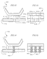
- FIG. 3 is a perspective view of the two layer corrugated printed circuit board of FIG. 2 .
- FIG. 8 is a top view of a portion of the interconnect of FIG. 7 including three lines of a microstrip transmission line in accordance with one embodiment of the invention.
- FIG. 11 is an exploded cross sectional view of the interconnect of FIG. 10 taken along section A-A.
- FIG. 12 is a cross sectional view of the interconnect of FIG. 10 illustrating a through hole extending through the flat flex layer and the adhesive layer to a conductor pad positioned on the folded flex layer of the interconnect.
- Embodiments of the corrugated PCBs described herein incorporate this same principle when they include arches in the corrugated medium. These arches are known as flutes and when anchored to a linerboard with an adhesive, they resist bending and pressure from all directions.
- Corrugated fiberboard, or combined board has two main components: the linerboard and the medium. Both are made of a special kind of heavy paper called container board for cardboard applications (e.g., boxes). Linerboard is the flat facing that adheres to the medium. The medium is the wavy, fluted paper in between the liners.
- the corrugation manufacturing processes are most commonly used to make boxes having one layer of fluting between two smooth sheets.
- the arches form rigid columns, capable of supporting a great deal of weight.
- the space in between the flutes acts as a cushion to protect the container's contents.
- the flutes also serve as an insulator, providing some product protection from sudden temperature changes.
- the vertical liner board provides more strength and protects the flutes from damage. Flutes come in several standard shapes or flute profiles.
- FIG. 7 is a close up view of an interconnect 300 between a folded flex layer 310 and a flat flex layer 312 of a corrugated printed circuit board in accordance with one embodiment of the invention.
- the interconnect 300 further includes a dielectric adhesive layer 311 or spacer disposed between the folded flex layer 310 and the flat flex layer 312.
- An RF communication signal 313 passes along the flat flex layer 312 toward and through the adhesive layer 311 and then along the folded flex layer 310.
- the flat flex layer 312 is configured as a microstrip transmission line or microstripline for passing the RF communication signal 313.
- the RF communication signal 313 passes along the bottom of the flat layer 312, via signal conductor 315, from right to left, transitions to the folded layer 310 via the interconnect and continues along a bottom of the folded layer 310, via signal conductor 319.
- the RF communication signal 313 can follow other suitable paths along the flat and folded layers.
- the dielectric adhesive layer can have a dielectric constant of 3.5. In other embodiments, the dielectric adhesive layer can have other suitable dielectric constant values.
- the folded flex layer and the flat flex layer are configured as microstripline transmission lines. In other embodiments, the folded flex layer and the flat flex layer can be configured to support other suitable types of transmission lines.
- an RF communication signal can pass along the flat flex layer 412 toward and through the adhesive layer 411 and then along the folded flex layer 410 or vice versa.
- the folded flex layer 410 is configured as a microstrip transmission line or microstripline for passing the RF communication signal.
- the flat layer 410 has a signal conductor 419, or microstripline, disposed along a bottom surface of the folded layer 410 and a groundplane conductor 421 disposed along a top surface of the flat layer 410.
- the process first designs and fabricates (501) a bottom flexible circuit, or flex circuit, with a hole and an annular ring at preselected attachment locations on a top surface of the bottom flex circuit.
- the process also designs and fabricates (502) a top flexible circuit with conductive pads at preselected attachment locations, that correspond to the attachment locations of the bottom flex circuit, on a bottom surface of the top flex circuit.
- the process can mechanically attach the flex circuits using multiple sub-processes.
- the process aligns (506) and fusion bonds (507) the flex circuits.
- the aligning can include aligning the top and bottom flex circuits so that the holes are in line with the pads.
- a second sub-process (dashed arrow path (2)), the process dispenses (505) a non-conductive paste on the top and/or bottom flex circuits. The process then aligns (506) the flex circuits and bonds (508) the common flat areas of the flex circuits together using heat and pressure.
Abstract
Description
- This invention was made with Government support from the Defense Advanced Research Projects Agency (DARPA) for the Integrated Sensor Is Structure (ISIS) program and under contract number FA8750-06-C-0048. The U.S. Government has certain rights in this invention.
- The present invention relates generally to printed circuit boards for use in communication systems. More specifically, the invention relates to multi-layer microwave corrugated printed circuit boards and methods for interconnecting the printed circuit boards.
- Next generation large area multifunction active arrays for applications such as space and airborne based antennas need to be lighter weight, lower cost and more conformal than what can be achieved with current active array architecture and multilayer active panel array development. These space and airborne antennas can be used for radar and communication systems, including platforms such as micro-satellites and stratospheric airships.
- The trend toward thinner and lighter multilayer mixed signal printed circuit board (PCB) panels integrating monolithic microwave integrated circuit (MMIC) and digital integrated circuits as well as power components is driven by installation requirements for these future platforms such as airships and micro-satellites. Minimizing the weight of these panels and the devices located thereon while maintaining panel strength sufficient to be part of an aircraft secondary structure are important design considerations. Conventional PCB construction for multi-layer mixed signal panels can be too complex and heavy to meet weight reduction requirements. A number of challenges for meeting the weight reduction requirements exist. For example, in conventional PCB construction, the circuit layers are generally laminated together with full sheets of bond ply adhesive film, which can contribute significantly to the weight of the panel. Accordingly, there is a need for a light weight PCB assembly that provides robust structural characteristics.
- Aspects of the invention relate to a multi-layer microwave corrugated printed circuit board. In one embodiment, the invention relates to a method for interconnecting components of a corrugated printed circuit board, the components including a first flexible layer having a first signal line on a surface of the first flexible layer and a second flexible layer having a second signal line on a surface of the second flexible layer, the method including forming at least one first hole in the first flexible layer, forming a conductive pad on the second flexible layer, forming at least one second hole in a non-conductive adhesive layer, aligning the at least one second hole with the at least one first hole and the conductive pad, bonding the first flexible layer and the second flexible layer, with the non-conductive adhesive layer disposed there between, and filling the at least one first hole and the at least one second hole with a conductive paste to electrically couple the first signal line with the second signal line.
- In another embodiment, the invention relates to an interconnect assembly for a corrugated printed circuit board, the interconnect assembly including a first flexible layer having a first signal line on a surface of the first flexible layer, the first flexible layer including a first hole, a second flexible layer having a second signal line on a surface of the second flexible layer, the second flexible layer including a conductive pad, a non-conductive adhesive layer having a second hole, the non-conductive adhesive layer disposed between, and coupled with, the first flexible layer and the second flexible layer, wherein the first hole, the second hole, and conductive pad are aligned such that the first hole and second hole include a third hole, and conductive paste disposed within the third hole to electrically couple the first signal line and the second signal line.
-
FIG. 1 is a side view of a corrugated printed circuit board in accordance with one embodiment of the invention. -
FIG. 2 is a exploded perspective view of a two layer corrugated printed circuit board in accordance with one embodiment of the invention. -
FIG. 3 is a perspective view of the two layer corrugated printed circuit board ofFIG. 2 . -
FIG. 4 is a exploded perspective view of the two layer corrugated printed circuit board ofFIG. 2 in accordance with one embodiment of the invention. -
FIG. 5 is a perspective view of the two layer corrugated printed circuit board ofFIG. 4 . -
FIG. 6 is a perspective view of a number of corrugated printed circuit boards having different widths in accordance with one embodiment of the invention. -
FIG. 7 is a close up view of an interconnect between a folded flex layer and a flat flex layer of a corrugated printed circuit board in accordance with one embodiment of the invention. -
FIG. 8 is a top view of a portion of the interconnect ofFIG. 7 including three lines of a microstrip transmission line in accordance with one embodiment of the invention. -
FIG. 9 is a cross sectional inverted view of the flat flex layer ofFIG. 7 in accordance with one embodiment of the invention. -
FIG. 10 is an exploded cross sectional view of an interconnect of a folded flex layer and a flat flex layer with an adhesive layer positioned there between in accordance with one embodiment of the invention. -
FIG. 11 is an exploded cross sectional view of the interconnect ofFIG. 10 taken along section A-A. -
FIG. 12 is a cross sectional view of the interconnect ofFIG. 10 illustrating a through hole extending through the flat flex layer and the adhesive layer to a conductor pad positioned on the folded flex layer of the interconnect. -
FIG. 13 is a cross sectional view of the interconnect ofFIG. 10 taken along the section A-A which illustrates three through holes extending through the flat flex layer and the adhesive layer to conductor pads positioned on the folded flex layer of the interconnect. -
FIG. 14 is a view of the interconnect ofFIG. 12 after conductive paste has been inserted into the through hole. -
FIG. 15 is a view of the interconnect ofFIG. 13 after conductive paste has been inserted into the three through holes. -
FIG. 16 is a flow chart of a process for assembling a corrugated printed circuit board in accordance with one embodiment of the invention. -
FIG. 17a-17c are assembly drawings of a process for assembling a corrugated printed circuit board in accordance with one embodiment of the invention. -
FIG. 18a-18c are assembly drawings of another process for assembling a corrugated printed circuit board in accordance with one embodiment of the invention. -
FIG. 19 is a flow chart of a process for forming an interconnect for a corrugated printed circuit board in accordance with one embodiment of the invention. - Referring now to the drawings, embodiments of systems and methods for interconnecting components of corrugated printed circuit boards (PCBs) are illustrated. In a number of embodiments, the corrugated PCBs include a first flexible layer having a first signal line on a surface of the first flexible layer and a second flexible layer having a second signal line on a surface of the second flexible layer. Embodiments of methods for forming an interconnect between the first and second layers can include forming a first hole in the first flexible layer, a conductive pad on the second flexible layer, and a second hole in a non-conductive adhesive layer disposed between the first and second layers, aligning the second hole with the first hole and the conductive pad, bonding the first flexible layer and the second flexible layer, and filling the first hole and the second hole with a conductive paste to electrically couple the first signal line with the second signal line.
- In several embodiments, the first layer includes multiple through holes aligned with corresponding through holes in the non-conductive adhesive layer and multiple pads on the second layer. For example, in one embodiment, the first layer includes three through holes aligned with three through holes in the non-conductive adhesive layer and three pads on the second layer. In one embodiment, the first layer is a flat flexible circuit layer and the second layer is a folded flexible circuit layer. Together the layers can form a corrugated circuit board structure. In another embodiment, the first layer is a folded flexible circuit layer and the second layer is a flat flexible circuit layer. In some embodiments, the corrugated PCBs can include more than two layers. In a number of embodiments, interconnects are formed at multiple locations on surfaces of the first and second layers.
- While not bound by any particular theory, architects have known for years that an arch with the proper curve is the strongest way to span a given space. Embodiments of the corrugated PCBs described herein incorporate this same principle when they include arches in the corrugated medium. These arches are known as flutes and when anchored to a linerboard with an adhesive, they resist bending and pressure from all directions. Corrugated fiberboard, or combined board, has two main components: the linerboard and the medium. Both are made of a special kind of heavy paper called container board for cardboard applications (e.g., boxes). Linerboard is the flat facing that adheres to the medium. The medium is the wavy, fluted paper in between the liners.
- The corrugation manufacturing processes are most commonly used to make boxes having one layer of fluting between two smooth sheets. When a piece of combined board is placed on its end, the arches form rigid columns, capable of supporting a great deal of weight. When pressure is applied to the side of the board, the space in between the flutes acts as a cushion to protect the container's contents. The flutes also serve as an insulator, providing some product protection from sudden temperature changes. At the same time, the vertical liner board provides more strength and protects the flutes from damage. Flutes come in several standard shapes or flute profiles.
- Embodiments of multi-layer corrugated printed circuit boards can be made of flexible circuit board material configured in an alternating combination of arched layers between smooth sheets. In some embodiments, the corrugated PCBs are used as with microwave and/or mixed signal designs. Corrugation is applied to the manufacturing of multi-layer printed flex circuit boards to created extremely durable, versatile, economical and lightweight assemblies of microwave multi-chip mixed signal electronic panels used for airborne platforms such as airships and micro-satellites where weight and cost are important factors. Microwave, digital and power integrated circuits (ICs) can be attached with reflowed solder paste on top or in between the layer and folds as shown in
FIG. 1 using standard flip chip surface mounting techniques. Microwave, digital and power signal traces can be routed along the fluted flex layers. Depending on the desired weight, component density and panel strength for a particular application, there are many types and combinations of corrugated layers available, each with different flute sizes and thicknesses. These formed layers, such as a wafer pattern, can offer enhanced structure, routing flexibility and functionality. -
FIG. 1 is a side view of a corrugated printedcircuit board 100 in accordance with one embodiment of the invention. In some embodiments, the corrugated PCB can be used in conjunction with an active array antenna for a radar or a communication system. The corrugated printedcircuit board 100 includes a level oneassembly 102, a level twoassembly 104 and a level threeassembly 106. The level oneassembly 102 can include one or more apertures, an radio frequency (RF) feed, electronic components and power and communication signals. The level twoassembly 104 can include an RF feed, electronic components and power and communication signals. The level threeassembly 106 can also include an RF feed, electronic components and power and communication signals. An example of a printed circuit board having a multiple assembly levels is described inU.S. Pat. No. 7,525,498 , the entire content of which is incorporated herein by reference. -
FIG. 2 is a exploded perspective view of a two layer corrugated printedcircuit board 200 in accordance with one embodiment of the invention. The corrugated printedcircuit board 200 includes a top flatflexible layer 208, a first folded or flutedflexible layer 210, a middle flatflexible layer 212, a second folded or flutedflexible layer 214, and a bottom flatflexible layer 216. In other embodiments, the corrugated PCB can include more than two fluted layers and more than three flat layers. - In the embodiment illustrated in
FIG. 2 , the flutes of the first or upperfluted layer 210 extend in the same direction as the flutes of the second or lowerfluted layer 214. In other embodiments, the flutes of the upper fluted layer and the lower fluted layers can extend in different directions. In one embodiment, the flutes of the upper fluted layer extend in a direction that is perpendicular to the flutes of the lower fluted layer, or vice versa. In other embodiments, additional fluted layers are included and the flutes of each fluted layer can extend in the same direction, or in different directions. In the embodiment illustrated inFIG. 2 , the fluted layers have a specific height and width for the flutes. In other embodiments, the fluted layers can have other heights and widths for the flutes. -
FIG. 3 is a perspective view of the two layer corrugated printedcircuit board 200 ofFIG. 2 . -
FIG. 4 is a exploded perspective view of the two layer corrugated printedcircuit board 200 ofFIG. 2 in accordance with one embodiment of the invention. The twolayer PCB 200 includes all of the same components of the embodiment illustrated inFIG. 2 , except that the flutes of the second flutedflexible layer 215 extend in a direction perpendicular to the flutes of the first flutedflexible layer 210. -
FIG. 5 is a perspective view of the two layer corrugated printed circuit board ofFIG. 4 . -
FIG. 6 is a perspective view of a number of corrugated printed circuit boards having different widths in accordance with one embodiment of the invention. Embodiments of corrugated printed circuit boards for the present invention can include flutes having several standard shapes or flute profiles (A, B, C, E, F, etc.) as shown inFigure 6 . The A-flute was the first to be developed and is one of the largest flute profiles. The B-flute was next and is much smaller. The C-flute followed and is between A and B in size. The E-flute is smaller than the B-flute and the F-flute is smaller yet. In addition to these five profiles, new flute profiles, both larger and smaller than those listed here, can be created for more specialized boards. Generally, larger flute profiles deliver greater vertical compression strength and cushioning. Smaller flute profiles provide enhanced structural capabilities. Different flute profiles can be combined in one piece of combined board. For instance, in a triple wall board, one layer of medium might be A-flute while the other two layers may be C-flute. Mixing flute profiles in this way allows designers to manipulate the compression strength, cushioning strength and total thickness of the combined board to suit requirements for particular applications. -
FIG. 7 is a close up view of aninterconnect 300 between a foldedflex layer 310 and aflat flex layer 312 of a corrugated printed circuit board in accordance with one embodiment of the invention. Theinterconnect 300 further includes a dielectricadhesive layer 311 or spacer disposed between the foldedflex layer 310 and theflat flex layer 312. AnRF communication signal 313 passes along theflat flex layer 312 toward and through theadhesive layer 311 and then along the foldedflex layer 310. InFIG. 7 , theflat flex layer 312 is configured as a microstrip transmission line or microstripline for passing theRF communication signal 313. As such, theflat layer 312 has asignal conductor 315 disposed along a bottom surface of theflat layer 312 and agroundplane conductor 317 disposed along a top surface of theflat layer 312. InFIG. 7 , the foldedflex layer 310 is also configured as a microstrip transmission line or microstripline for passing theRF communication signal 313. As such, theflat layer 310 has asignal conductor 319, or microstripline, disposed along a bottom surface of the foldedlayer 310 and agroundplane conductor 321 disposed along a top surface of theflat layer 310. - In the embodiment illustrated in
FIG. 7 , theRF communication signal 313 passes along the bottom of theflat layer 312, viasignal conductor 315, from right to left, transitions to the foldedlayer 310 via the interconnect and continues along a bottom of the foldedlayer 310, viasignal conductor 319. In other embodiments, theRF communication signal 313 can follow other suitable paths along the flat and folded layers. In one embodiment, the dielectric adhesive layer can have a dielectric constant of 3.5. In other embodiments, the dielectric adhesive layer can have other suitable dielectric constant values. In the embodiment illustrated inFIG. 7 , the folded flex layer and the flat flex layer are configured as microstripline transmission lines. In other embodiments, the folded flex layer and the flat flex layer can be configured to support other suitable types of transmission lines. -
FIG. 8 is a top view of a portion of theinterconnect 300 ofFIG. 7 showing a three wire interconnect for connecting signal lines of a microstrip transmission line in accordance with one embodiment of the invention. The three wire interconnect includes amiddle line interconnect 323 for an RF signal, and two outer line interconnects 325 and 327 for the associated ground plane signals. -
FIG. 9 is a cross sectional inverted view of theflat flex layer 312 ofFIG. 7 in accordance with one embodiment of the invention. Theflat flex layer 312 is configured as a microstrip transmission line which includes thesignal conductor trace 315 on one surface of theflat layer 312 and aground plane 317 disposed on an opposite side of theflat layer 312, where the surfaces are separated by adielectric layer 329. In one embodiment, the dielectric layer can have a dielectric constant of 2.9. In other embodiments, the dielectric layer can have other suitable dielectric constant values. -
FIG. 10 is an exploded cross sectional view of aninterconnect 400 of a foldedflex layer 410 and aflat flex layer 412 with anadhesive layer 411 positioned there between in accordance with one embodiment of the invention.FIG. 11 is an exploded cross sectional view of theinterconnect 400 ofFIG. 10 taken along section A-A. - When the interconnect is assembled, an RF communication signal can pass along the
flat flex layer 412 toward and through theadhesive layer 411 and then along the foldedflex layer 410 or vice versa. The foldedflex layer 410 is configured as a microstrip transmission line or microstripline for passing the RF communication signal. As such, theflat layer 410 has asignal conductor 419, or microstripline, disposed along a bottom surface of the foldedlayer 410 and agroundplane conductor 421 disposed along a top surface of theflat layer 410. - To form the
interconnect 400, the foldedlayer 410 further includesconductive pads holes 440.Conductive pad 434a is used to provide a pathway for the RF communication signal, whileconductive pads holes 440. To form theinterconnect 400, theadhesive layer 411 includes throughholes - The
flat flex layer 412 is also configured as a microstrip transmission line or microstripline for passing the RF communication signal. As such, theflat layer 412 has asignal conductor 415 disposed along a bottom surface of theflat layer 412 and agroundplane conductor 417 disposed along a top surface of theflat layer 412. To form theinterconnect 400, theflat layer 412 further includes throughholes holes top groudplane layer 417 and bottomRF signal layer 415 for making electrical contact with circuit traces. The throughholes -
FIG. 12 is a cross sectional view of theinterconnect 400 ofFIG. 10 illustrating a throughhole 433a extending through theflat flex layer 412 and theadhesive layer 411 to aconductor pad 434a positioned on the foldedflex layer 410 of the interconnect. Adhesive layer throughhole 432a and flat flex layer throughhole 436a are aligned to form throughhole 433a extending through both layers to theconductor pad 434a positioned on the foldedflex layer 410. -
FIG. 13 is a cross sectional view of theinterconnect 400 ofFIG. 10 taken along the section A-A which illustrates three through holes (433a, 433b, 433c) extending through both theflat flex layer 412 and theadhesive layer 411 to the conductor pads (434a, 434b, 434c) positioned on the foldedflex layer 410 of the interconnect. -
FIG. 14 is a view of the interconnect ofFIG. 12 afterconductive paste 442 has been inserted into throughhole 433a. In some embodiments, the conductive paste also has adhesive properties. -
FIG. 15 is a view of the interconnect ofFIG. 13 afterconductive paste 442 has been inserted into the three through holes (433a, 433b, 433c). The conductive paste completes an electrical pathway for the RF communication and ground signals, and provides additional structural support for the interconnect. -
FIG. 16 is a flow chart of a process for assembling a corrugated printed circuit board in accordance with one embodiment of the invention. Theprocess 500 shows different paths to produce an interconnect that can be used to attach components of a corrugated printed circuit. In one embodiment, theprocess 500 produces a flexible circuit attachment using a conductive fill, disposed within an open hole of a bottom flex circuit, that forms an electrical interconnect between a conductor on the bottom flex circuit and a conductor on the top flex circuit. - The process first designs and fabricates (501) a bottom flexible circuit, or flex circuit, with a hole and an annular ring at preselected attachment locations on a top surface of the bottom flex circuit. The process also designs and fabricates (502) a top flexible circuit with conductive pads at preselected attachment locations, that correspond to the attachment locations of the bottom flex circuit, on a bottom surface of the top flex circuit. From
block 502, the process can mechanically attach the flex circuits using multiple sub-processes. In a first sub-process (solid arrow path), the process aligns (506) and fusion bonds (507) the flex circuits. The aligning can include aligning the top and bottom flex circuits so that the holes are in line with the pads. In a second sub-process (dashed arrow path (2)), the process dispenses (505) a non-conductive paste on the top and/or bottom flex circuits. The process then aligns (506) the flex circuits and bonds (508) the common flat areas of the flex circuits together using heat and pressure. - In a third sub-process (dashed arrow path (1)), the process precuts (503) holes in a non-conductive film adhesive where electrical connections are intended to be positioned. The process then aligns (504) the non-conductive adhesive on the bottom and/or top flex layers and tacks it into place. The process then aligns (506) the flex circuits and bonds (508) the common flat areas of the flex circuits together using heat and pressure. Once the top and bottom flex circuits have been attached, the process dispenses (509) conductive adhesive paste into the hole(s) to fill the area created by the hole and to thereby attach the bottom flex circuit with the pad of the top flex circuit. The process then cures (510) the conductive adhesive paste.
- In one embodiment, the process can perform the sequence of actions in any order. In another embodiment, the process can skip one or more of the actions. In other embodiments, one of more of the actions are performed simultaneously. In some embodiments, additional actions can be performed.
- In one embodiment, the top flex circuit can be a folded flex circuit/layer and the bottom flex circuit can be flat flex circuit/layer. In such case, the bottom/flat flex circuit includes the through hole and the top/folded flex circuit includes the pad(s). In another embodiment, the top flex circuit can be a flat flex circuit/layer and the bottom flex circuit can be folded flex circuit/layer. In such case, the bottom/folded flex circuit includes the through hole and the top/flat flex circuit includes the pad(s).
- In the process illustrated in
FIG. 16 , the process may at times refer to a single hole or pad. However, the process generally relates to use of multiple holes and pads. -
FIG. 17a-17c are assembly drawings of a process for assembling an interconnect for a corrugated printed circuit board in accordance with one embodiment of the invention. In the embodiment illustrated inFIG. 17a-17c , the top flex circuit is folded and the bottom flex circuit is flat.FIG. 17a illustrates an exploded cross sectional assembly view of the interconnect prior to bonding.FIG. 17b illustrates a cross sectional view of the bonded interconnect assembly prior to insertion of conductive paste.FIG. 17c illustrates a cross sectional view of the bonded interconnect assembly after the holes have been filled with conductive paste. In some embodiments, the conductive paste includes adhesive properties. -
FIG. 18a-18c are assembly drawings of a process for assembling an interconnect for a corrugated printed circuit board in accordance with one embodiment of the invention. In the embodiment illustrated inFIG. 18a-18c , the top flex circuit is flat and the bottom flex circuit is folded.FIG. 18a illustrates an exploded cross sectional assembly view of the interconnect prior to bonding.FIG. 18b illustrates a cross sectional view of the bonded interconnect assembly prior to an insertion of conductive paste.FIG. 18c illustrates a cross sectional view of the bonded interconnect assembly after the holes have been filled with conductive paste. In some embodiments, the conductive paste includes adhesive properties. -
FIG. 19 is a flow chart of aprocess 600 for forming an interconnect for a corrugated printed circuit board in accordance with one embodiment of the invention. In a number of embodiments, the corrugated PCB includes a first flexible layer having a first signal line on a surface of the first flexible layer and a second flexible layer having a second signal line on a surface of the second flexible layer. The process begins by forming (602) at least one first hole in the first flexible layer. In several embodiments, the first hole is a plated through hole coupled to the first signal line of the first layer. The process then forms (604) a conductive pad on the second flexible layer. In several embodiments, the conductive pad is coupled to the second signal line. The process then forms (606) at least one second hole in a non-conductive adhesive layer. The process then aligns (608) the second hole with the first hole and the conductive pad. The process then bonds (610) the first flexible layer and the second flexible layer with the adhesive layer positioned between the two layers. The process completes by filling (612) the first hole and the second hole with a conductive adhesive paste to couple the first and second signal lines. - In one embodiment, the first flexible layer is a folded flex circuit and the second flexible layer is a flat flex circuit. In another embodiment, the first flexible layer is a flat flex circuit and the second flexible layer is a folded flex circuit.
- In one embodiment, the process can perform the sequence of actions in any order. In another embodiment, the process can skip one or more of the actions. In other embodiments, one of more of the actions are performed simultaneously. In some embodiments, additional actions can be performed.
- In one embodiment, the bonding is achieved by a fusion bonding process. In another embodiment, the bonding is achieved by bonding the common flat areas of the first flexible layer and the second flexible layer together using heat and pressure. In some embodiments, the bonding process is achieved by adding a non-conductive adhesive film to the first flexible layer and/or the second flexible layer. In other embodiments, the bonding process is achieved by adding a non-conductive paste to the first flexible layer and/or the second flexible layer.
- While the above description contains many specific embodiments of the invention, these should not be construed as limitations on the scope of the invention, but rather as examples of specific embodiments thereof. Accordingly, the scope of the invention should be determined not by the embodiments illustrated, but by the appended claims and their equivalents.
Claims (15)
- A method for interconnecting components of a corrugated printed circuit board, the components comprising a first flexible layer having a first signal line on a surface of the first flexible layer and a second flexible layer having a second signal line on a surface of the second flexible layer, the method comprising:forming at least one first hole in the first flexible layer;forming a conductive pad on the second flexible layer;forming at least one second hole in a non-conductive adhesive layer;aligning the at least one second hole with the at least one first hole and the conductive pad;bonding the first flexible layer and the second flexible layer, with the non-conductive adhesive layer disposed there between; andfilling the at least one first hole and the at least one second hole with a conductive paste to electrically couple the first signal line with the second signal line.
- The method of claim 1:wherein the at least one first hole comprises:a first through hole for the first signal line;a second through hole for a first ground plane line; anda third through hole for a second ground plane line;wherein the at least one second hole comprises:a fourth through hole for the second signal line;a fifth through hole for a third ground plane line; anda sixth through hole for a fourth ground plane line;wherein the filling the at least one first hole and the at least one second hole with the conductive paste comprises filling the first through hole, the second through hole, the third through hole, the fourth through hole, the fifth through hole, and the sixth through hole with the conductive paste.
- The method of claim 1 or claim 2, wherein the conductive paste electrically couples a ground plane of the first flexible layer with a ground plane of the second flexible layer.
- The method of any preceding claim, further comprising adding a non-conductive adhesive layer to the second flexible layer prior to the bonding the first flexible layer and the second flexible layer.
- The method of any preceding claim, further comprising curing the conductive paste.
- The method of any preceding claim, wherein the components of the corrugated printed circuit board further comprise a third flexible layer and a fourth flexible layer.
- An interconnect assembly for a corrugated printed circuit board, the interconnect assembly comprising:a first flexible layer having a first signal line on a surface of the first flexible layer, the first flexible layer comprising a first hole;a second flexible layer having a second signal line on a surface of the second flexible layer, the second flexible layer comprising a conductive pad;a non-conductive adhesive layer having a second hole, the non-conductive adhesive layer disposed between, and coupled with, the first flexible layer and the second flexible layer, wherein the first hole, the second hole, and conductive pad are aligned such that the first hole and second hole comprise a third hole; andconductive paste disposed within the third hole to electrically couple the first signal line and the second signal line.
- The interconnect assembly of claim 7, wherein the first flexible layer is a folded flexible layer, and the second flexible layer is a flat flexible layer.
- The interconnect assembly of claim 7, wherein the first flexible layer is a flat flexible layer, and the second flexible layer is a folded flexible layer.
- The interconnect assembly of claim 7, claim 8 or claim 9:wherein the first hole comprises a first through hole for the first signal line;wherein the first flexible layer further comprises:a second through hole for coupling a ground plane of the first flexible layer; anda third through hole for coupling the ground plane of the first flexible layer;wherein the second hole comprises a fourth through hole for the second signal line; andwherein the second flexible layer further comprises:a fifth through hole for coupling a ground plane of the second flexible layer; anda sixth through hole for coupling to the ground plane of the second flexible layer.
- The interconnect assembly of any one of claims 7 to 10, wherein the conductive paste is a conductive adhesive paste.
- The interconnect assembly of any one of claims 7 to 11, further comprising a non-conductive adhesive layer disposed on the second flexible layer.
- The interconnect assembly of any one of claims 7 to 12, further comprising a third flexible layer and a fourth flexible layer.
- The interconnect assembly of claim 13, wherein the third flexible layer is a folded flexible layer, and the fourth flexible layer is a flat flexible layer.
- The interconnect assembly of claim 13:wherein the first flexible layer is a flat flexible layer, and the second flexible layer is a folded flexible layer;wherein the third flexible layer is a flat flexible layer, and the fourth flexible layer is a folded flexible layer;wherein the third flat flexible layer is coupled between the second folded flexible layer and the fourth folded flexible layer;wherein a flute of the second folded flexible layer extends in a first direction;wherein a flute of the fourth folded flexible layer extends in a second direction; andwherein the first direction and the second direction are not the same.
Applications Claiming Priority (1)
| Application Number | Priority Date | Filing Date | Title |
|---|---|---|---|
| US12/534,077 US20110024160A1 (en) | 2009-07-31 | 2009-07-31 | Multi-layer microwave corrugated printed circuit board and method |
Publications (1)
| Publication Number | Publication Date |
|---|---|
| EP2288242A1 true EP2288242A1 (en) | 2011-02-23 |
Family
ID=43037070
Family Applications (1)
| Application Number | Title | Priority Date | Filing Date |
|---|---|---|---|
| EP10251312A Withdrawn EP2288242A1 (en) | 2009-07-31 | 2010-07-23 | Multi-layer microwave corrugated printed circuit board and method |
Country Status (5)
| Country | Link |
|---|---|
| US (2) | US20110024160A1 (en) |
| EP (1) | EP2288242A1 (en) |
| JP (1) | JP5221606B2 (en) |
| KR (1) | KR101139581B1 (en) |
| IL (1) | IL206729A (en) |
Cited By (7)
| Publication number | Priority date | Publication date | Assignee | Title |
|---|---|---|---|---|
| EP2323467A1 (en) * | 2009-11-17 | 2011-05-18 | Raytheon Company | Process for fabricating an origami formed antenna radiating structure |
| US8043464B2 (en) | 2009-11-17 | 2011-10-25 | Raytheon Company | Systems and methods for assembling lightweight RF antenna structures |
| US8362856B2 (en) | 2009-11-17 | 2013-01-29 | Raytheon Company | RF transition with 3-dimensional molded RF structure |
| US9072164B2 (en) | 2009-11-17 | 2015-06-30 | Raytheon Company | Process for fabricating a three dimensional molded feed structure |
| US9491854B2 (en) | 2009-07-31 | 2016-11-08 | Raytheon Company | Multi-layer microwave corrugated printed circuit board and method |
| CN109727848A (en) * | 2018-12-29 | 2019-05-07 | 长江存储科技有限责任公司 | A kind of manufacturing method of three-dimensional storage |
| CN110581417A (en) * | 2018-06-07 | 2019-12-17 | 奥特斯奥地利科技与系统技术有限公司 | Deformation layer for short electrical connections between electrical device structures |
Families Citing this family (8)
| Publication number | Priority date | Publication date | Assignee | Title |
|---|---|---|---|---|
| USD669045S1 (en) * | 2010-05-19 | 2012-10-16 | Nippon Mektron, Ltd. | Flexible printed circuit board |
| USD669046S1 (en) * | 2010-05-19 | 2012-10-16 | Nippon Mektron, Ltd | Flexible printed circuit board |
| US20130224405A1 (en) * | 2012-02-23 | 2013-08-29 | Lockheed Martin Corporation | Electromagnetic meta-materials |
| WO2014125852A1 (en) * | 2013-02-14 | 2014-08-21 | 株式会社村田製作所 | Circuit substrate, and production method therefor |
| US20140264938A1 (en) * | 2013-03-14 | 2014-09-18 | Douglas R. Hackler, Sr. | Flexible Interconnect |
| JP1588722S (en) * | 2017-02-15 | 2017-10-23 | ||
| KR20200030411A (en) * | 2018-09-12 | 2020-03-20 | 엘지이노텍 주식회사 | Flexible circuit board and chip pakage comprising the same, and electronic device comprising the same |
| EP4197294A1 (en) * | 2020-09-16 | 2023-06-21 | Google LLC | Overlap joint flex circuit board interconnection |
Citations (6)
| Publication number | Priority date | Publication date | Assignee | Title |
|---|---|---|---|---|
| US3004229A (en) * | 1959-02-24 | 1961-10-10 | Sanders Associates Inc | High frequency transmission line |
| GB2064233A (en) * | 1979-11-14 | 1981-06-10 | Hitachi Ltd | Liquid crystal display device |
| JPH0851279A (en) * | 1994-08-05 | 1996-02-20 | Yazaki Corp | Method for connecting wiring board |
| JPH09281520A (en) * | 1996-04-10 | 1997-10-31 | Seiko Epson Corp | Method for connecting circuit board, liquid crystal display device and electronic apparatus |
| FR2871336A1 (en) * | 2004-06-02 | 2005-12-09 | Bree Ind Soc Par Actions Simpl | FLEX-RIGID PRINTED CIRCUIT BY COLLAGE |
| US7525498B2 (en) | 2006-10-11 | 2009-04-28 | Raytheon Company | Antenna array |
Family Cites Families (45)
| Publication number | Priority date | Publication date | Assignee | Title |
|---|---|---|---|---|
| US131451A (en) * | 1872-09-17 | Improvement in dish-washers | ||
| US231226A (en) * | 1880-08-17 | Telephone-transmitter | ||
| US165296A (en) * | 1875-07-06 | Improvement in wash-stands | ||
| US723548A (en) * | 1900-03-21 | 1903-03-24 | Holyoke Machine Company | Founder's molding-machine. |
| US4126508A (en) * | 1976-09-13 | 1978-11-21 | Boise Cascade Corporation | Apparatus for forming multi-flute-layer corrugated board |
| US4853660A (en) * | 1988-06-30 | 1989-08-01 | Raytheon Company | Integratable microwave devices based on ferromagnetic films disposed on dielectric substrates |
| US5097101A (en) | 1991-02-05 | 1992-03-17 | Tektronix, Inc. | Method of forming a conductive contact bump on a flexible substrate and a flexible substrate |
| US5343616B1 (en) | 1992-02-14 | 1998-12-29 | Rock Ltd | Method of making high density self-aligning conductive networks and contact clusters |
| US5262590A (en) * | 1992-04-27 | 1993-11-16 | Sheldahl, Inc. | Impedance controlled flexible circuits with fold-over shields |
| US5408240A (en) | 1993-12-23 | 1995-04-18 | Hughes Aircraft Company | Suspended stripline RF feed with orthogonal coaxial transitions and plastic housing |
| US5633615A (en) | 1995-12-26 | 1997-05-27 | Hughes Electronics | Vertical right angle solderless interconnects from suspended stripline to three-wire lines on MIC substrates |
| JP3574308B2 (en) * | 1997-09-02 | 2004-10-06 | アルプス電気株式会社 | Laminated substrate and data input device using the same |
| US6018326A (en) | 1997-09-29 | 2000-01-25 | Ericsson Inc. | Antennas with integrated windings |
| US6061245A (en) * | 1998-01-22 | 2000-05-09 | International Business Machines Corporation | Free standing, three dimensional, multi-chip, carrier package with air flow baffle |
| JPH11284332A (en) * | 1998-03-30 | 1999-10-15 | Jsr Corp | Adhesive sheet for laminating wiring board and manufacture thereof, and laminated connector and manufacture thereof |
| JPH11330645A (en) * | 1998-05-19 | 1999-11-30 | Matsushita Electric Ind Co Ltd | Printed board with enlarged copper foils of surface layer and inner layer |
| JP2000332419A (en) * | 1999-05-24 | 2000-11-30 | Hitachi Ltd | Multilayer printed substrate and liquid crystal display device |
| JP3654095B2 (en) * | 1999-11-05 | 2005-06-02 | 三菱電機株式会社 | High frequency printed wiring board and method for manufacturing the same |
| JP2001189609A (en) * | 1999-12-28 | 2001-07-10 | Mitsubishi Electric Corp | Microstrip line connector |
| US6366185B1 (en) | 2000-01-12 | 2002-04-02 | Raytheon Company | Vertical interconnect between coaxial or GCPW circuits and airline via compressible center conductors |
| JP3495305B2 (en) * | 2000-02-02 | 2004-02-09 | Necエレクトロニクス株式会社 | Semiconductor device and semiconductor module |
| US6444921B1 (en) * | 2000-02-03 | 2002-09-03 | Fujitsu Limited | Reduced stress and zero stress interposers for integrated-circuit chips, multichip substrates, and the like |
| US6871396B2 (en) * | 2000-02-09 | 2005-03-29 | Matsushita Electric Industrial Co., Ltd. | Transfer material for wiring substrate |
| US7298331B2 (en) | 2000-03-13 | 2007-11-20 | Rcd Technology, Inc. | Method for forming radio frequency antenna |
| US6696163B2 (en) * | 2000-07-18 | 2004-02-24 | 3M Innovative Properties Company | Liquid crystal polymers for flexible circuits |
| JP2003347503A (en) * | 2002-05-30 | 2003-12-05 | Hitachi Ltd | Semiconductor device and method of manufacturing the same, and semiconductor mounting structure |
| JP2004221345A (en) * | 2003-01-15 | 2004-08-05 | Sumitomo Electric Ind Ltd | Flexible board and method of connecting the same |
| US6992629B2 (en) * | 2003-09-03 | 2006-01-31 | Raytheon Company | Embedded RF vertical interconnect for flexible conformal antenna |
| JP4253280B2 (en) | 2003-12-05 | 2009-04-08 | 三井金属鉱業株式会社 | Method for manufacturing printed wiring board |
| US7057563B2 (en) * | 2004-05-28 | 2006-06-06 | Raytheon Company | Radiator structures |
| US7109943B2 (en) * | 2004-10-21 | 2006-09-19 | The Boeing Company | Structurally integrated antenna aperture and fabrication method |
| KR101293400B1 (en) * | 2005-07-29 | 2013-08-05 | 타이코 일렉트로닉스 코포레이션 | Circuit protection device having thermally coupled mov overvoltage element and pptc overcurrent element |
| US7645942B2 (en) | 2005-12-09 | 2010-01-12 | Xerox Corporation | Electrical interconnect with maximized electrical contact |
| US7463198B2 (en) * | 2005-12-16 | 2008-12-09 | Applied Radar Inc. | Non-woven textile microwave antennas and components |
| JP2007221077A (en) * | 2006-02-20 | 2007-08-30 | Fujikura Ltd | Connection structure and connection method for printed wiring board |
| US20090165296A1 (en) | 2006-04-04 | 2009-07-02 | Yoash Carmi | Patterns of conductive objects on a substrate and method of producing thereof |
| US7992293B2 (en) | 2006-04-04 | 2011-08-09 | Hanita Coatings R.C.A. Ltd | Method of manufacturing a patterned conductive layer |
| US7645941B2 (en) * | 2006-05-02 | 2010-01-12 | Multi-Fineline Electronix, Inc. | Shielded flexible circuits and methods for manufacturing same |
| US8059049B2 (en) | 2006-10-11 | 2011-11-15 | Raytheon Company | Dual band active array antenna |
| US8026863B2 (en) | 2006-10-11 | 2011-09-27 | Raytheon Company | Transmit/receive module communication and control architechture for active array |
| US20110024160A1 (en) | 2009-07-31 | 2011-02-03 | Clifton Quan | Multi-layer microwave corrugated printed circuit board and method |
| US8127432B2 (en) | 2009-11-17 | 2012-03-06 | Raytheon Company | Process for fabricating an origami formed antenna radiating structure |
| US8362856B2 (en) * | 2009-11-17 | 2013-01-29 | Raytheon Company | RF transition with 3-dimensional molded RF structure |
| US8043464B2 (en) * | 2009-11-17 | 2011-10-25 | Raytheon Company | Systems and methods for assembling lightweight RF antenna structures |
| US9072164B2 (en) * | 2009-11-17 | 2015-06-30 | Raytheon Company | Process for fabricating a three dimensional molded feed structure |
-
2009
- 2009-07-31 US US12/534,077 patent/US20110024160A1/en not_active Abandoned
-
2010
- 2010-06-30 IL IL206729A patent/IL206729A/en active IP Right Grant
- 2010-07-23 EP EP10251312A patent/EP2288242A1/en not_active Withdrawn
- 2010-07-30 KR KR1020100074338A patent/KR101139581B1/en active IP Right Grant
- 2010-07-30 JP JP2010171363A patent/JP5221606B2/en active Active
-
2013
- 2013-04-18 US US13/865,730 patent/US9491854B2/en active Active
Patent Citations (6)
| Publication number | Priority date | Publication date | Assignee | Title |
|---|---|---|---|---|
| US3004229A (en) * | 1959-02-24 | 1961-10-10 | Sanders Associates Inc | High frequency transmission line |
| GB2064233A (en) * | 1979-11-14 | 1981-06-10 | Hitachi Ltd | Liquid crystal display device |
| JPH0851279A (en) * | 1994-08-05 | 1996-02-20 | Yazaki Corp | Method for connecting wiring board |
| JPH09281520A (en) * | 1996-04-10 | 1997-10-31 | Seiko Epson Corp | Method for connecting circuit board, liquid crystal display device and electronic apparatus |
| FR2871336A1 (en) * | 2004-06-02 | 2005-12-09 | Bree Ind Soc Par Actions Simpl | FLEX-RIGID PRINTED CIRCUIT BY COLLAGE |
| US7525498B2 (en) | 2006-10-11 | 2009-04-28 | Raytheon Company | Antenna array |
Cited By (10)
| Publication number | Priority date | Publication date | Assignee | Title |
|---|---|---|---|---|
| US9491854B2 (en) | 2009-07-31 | 2016-11-08 | Raytheon Company | Multi-layer microwave corrugated printed circuit board and method |
| EP2323467A1 (en) * | 2009-11-17 | 2011-05-18 | Raytheon Company | Process for fabricating an origami formed antenna radiating structure |
| US8043464B2 (en) | 2009-11-17 | 2011-10-25 | Raytheon Company | Systems and methods for assembling lightweight RF antenna structures |
| US8127432B2 (en) | 2009-11-17 | 2012-03-06 | Raytheon Company | Process for fabricating an origami formed antenna radiating structure |
| US8362856B2 (en) | 2009-11-17 | 2013-01-29 | Raytheon Company | RF transition with 3-dimensional molded RF structure |
| US8453314B2 (en) | 2009-11-17 | 2013-06-04 | Raytheon Company | Process for forming channels in a flexible circuit substrate using an elongated wedge and a channel shaped receptacle |
| US9072164B2 (en) | 2009-11-17 | 2015-06-30 | Raytheon Company | Process for fabricating a three dimensional molded feed structure |
| CN110581417A (en) * | 2018-06-07 | 2019-12-17 | 奥特斯奥地利科技与系统技术有限公司 | Deformation layer for short electrical connections between electrical device structures |
| EP3579669A3 (en) * | 2018-06-07 | 2020-04-29 | AT & S Austria Technologie & Systemtechnik Aktiengesellschaft | Deformed layer for short electric connection between structures of electric device |
| CN109727848A (en) * | 2018-12-29 | 2019-05-07 | 长江存储科技有限责任公司 | A kind of manufacturing method of three-dimensional storage |
Also Published As
| Publication number | Publication date |
|---|---|
| US20110024160A1 (en) | 2011-02-03 |
| US9491854B2 (en) | 2016-11-08 |
| IL206729A0 (en) | 2010-12-30 |
| KR101139581B1 (en) | 2012-04-27 |
| IL206729A (en) | 2015-08-31 |
| JP2011035401A (en) | 2011-02-17 |
| JP5221606B2 (en) | 2013-06-26 |
| US20130319732A1 (en) | 2013-12-05 |
| KR20110013333A (en) | 2011-02-09 |
Similar Documents
| Publication | Publication Date | Title |
|---|---|---|
| US9491854B2 (en) | Multi-layer microwave corrugated printed circuit board and method | |
| CN101460018B (en) | Printed circuit board, manufacturing method and radio-frequency apparatus thereof | |
| WO2017047396A1 (en) | Antenna-integrated communication module and method for manufacturing same | |
| TWI463736B (en) | Radio frequency (rf) integrated circuit (ic) packages with integrated aperture-coupled patch antenna(s) | |
| JP4463102B2 (en) | Multi-layer stripline assembly interconnection and interconnection method | |
| US20050269693A1 (en) | Assembly including vertical and horizontal joined circuit panels | |
| US8076591B2 (en) | Circuit boards | |
| US20100163282A1 (en) | Printed wiring board, method for manufacturing printed wiring board, and electric device | |
| CN102137541A (en) | Flex-rigid wiring board and method for manufacturing the same | |
| CN105050313B (en) | The method of multilager base plate and manufacture multilager base plate | |
| US20110115578A1 (en) | Rf transition with 3-dimensional molded rf structure | |
| US20190141831A1 (en) | Multilayer substrate | |
| JP2011035345A (en) | Semiconductor device module, electronic circuit unit, electronic device, and method of manufacturing semiconductor device module | |
| US8547280B2 (en) | Systems and methods for exciting long slot radiators of an RF antenna | |
| US20070107935A1 (en) | Method and apparatus for electrically connecting printed circuit boards or other panels | |
| US8227699B2 (en) | Printed circuit board | |
| JP2009164577A (en) | Laminated printed wiring board for controlling spurious rf emission capability/characteristics | |
| JP6569826B2 (en) | Antenna module | |
| US9974160B1 (en) | Interconnection system for a multilayered radio frequency circuit and method of fabrication | |
| US20120099285A1 (en) | Laminated substrate with coils | |
| US11178765B2 (en) | Electronic device | |
| US8841561B1 (en) | High performance PCB | |
| JP2006108741A (en) | High-frequency power distributor/combiner | |
| CN101015236A (en) | Wiring board | |
| CN112054299A (en) | Navigation antenna |
Legal Events
| Date | Code | Title | Description |
|---|---|---|---|
| PUAI | Public reference made under article 153(3) epc to a published international application that has entered the european phase |
Free format text: ORIGINAL CODE: 0009012 |
|
| AK | Designated contracting states |
Kind code of ref document: A1 Designated state(s): AL AT BE BG CH CY CZ DE DK EE ES FI FR GB GR HR HU IE IS IT LI LT LU LV MC MK MT NL NO PL PT RO SE SI SK SM TR |
|
| AX | Request for extension of the european patent |
Extension state: BA ME RS |
|
| 17P | Request for examination filed |
Effective date: 20110801 |
|
| GRAP | Despatch of communication of intention to grant a patent |
Free format text: ORIGINAL CODE: EPIDOSNIGR1 |
|
| RIC1 | Information provided on ipc code assigned before grant |
Ipc: H05K 3/46 20060101ALI20160426BHEP Ipc: H05K 3/36 20060101AFI20160426BHEP Ipc: H05K 1/02 20060101ALI20160426BHEP Ipc: H05K 3/40 20060101ALI20160426BHEP Ipc: H05K 1/14 20060101ALI20160426BHEP |
|
| INTG | Intention to grant announced |
Effective date: 20160518 |
|
| STAA | Information on the status of an ep patent application or granted ep patent |
Free format text: STATUS: THE APPLICATION IS DEEMED TO BE WITHDRAWN |
|
| 18D | Application deemed to be withdrawn |
Effective date: 20160929 |