EP2283935A1 - Système de convertisseur à ultrasons et son procédé de fonctionnement - Google Patents
Système de convertisseur à ultrasons et son procédé de fonctionnement Download PDFInfo
- Publication number
- EP2283935A1 EP2283935A1 EP09010474A EP09010474A EP2283935A1 EP 2283935 A1 EP2283935 A1 EP 2283935A1 EP 09010474 A EP09010474 A EP 09010474A EP 09010474 A EP09010474 A EP 09010474A EP 2283935 A1 EP2283935 A1 EP 2283935A1
- Authority
- EP
- European Patent Office
- Prior art keywords
- electrodes
- substrate
- active layer
- electrically
- emitted
- Prior art date
- Legal status (The legal status is an assumption and is not a legal conclusion. Google has not performed a legal analysis and makes no representation as to the accuracy of the status listed.)
- Ceased
Links
- 238000000034 method Methods 0.000 title claims abstract description 11
- 238000002604 ultrasonography Methods 0.000 title description 7
- 239000000758 substrate Substances 0.000 claims abstract description 38
- 239000000463 material Substances 0.000 claims abstract description 17
- 239000004020 conductor Substances 0.000 claims description 6
- 239000011159 matrix material Substances 0.000 claims description 6
- 239000010409 thin film Substances 0.000 claims description 3
- 239000010931 gold Substances 0.000 description 4
- 230000004913 activation Effects 0.000 description 3
- 229910052737 gold Inorganic materials 0.000 description 3
- 238000004519 manufacturing process Methods 0.000 description 3
- 238000005476 soldering Methods 0.000 description 3
- 239000000853 adhesive Substances 0.000 description 2
- 238000004026 adhesive bonding Methods 0.000 description 2
- 230000001070 adhesive effect Effects 0.000 description 2
- 239000000919 ceramic Substances 0.000 description 2
- 230000008878 coupling Effects 0.000 description 2
- 238000010168 coupling process Methods 0.000 description 2
- 238000005859 coupling reaction Methods 0.000 description 2
- 230000007547 defect Effects 0.000 description 2
- 238000001514 detection method Methods 0.000 description 2
- 238000005259 measurement Methods 0.000 description 2
- 229910052751 metal Inorganic materials 0.000 description 2
- 239000002184 metal Substances 0.000 description 2
- 238000001465 metallisation Methods 0.000 description 2
- 238000009659 non-destructive testing Methods 0.000 description 2
- 238000005240 physical vapour deposition Methods 0.000 description 2
- 238000001020 plasma etching Methods 0.000 description 2
- BASFCYQUMIYNBI-UHFFFAOYSA-N platinum Chemical compound [Pt] BASFCYQUMIYNBI-UHFFFAOYSA-N 0.000 description 2
- RYGMFSIKBFXOCR-UHFFFAOYSA-N Copper Chemical compound [Cu] RYGMFSIKBFXOCR-UHFFFAOYSA-N 0.000 description 1
- 239000011149 active material Substances 0.000 description 1
- 229910052782 aluminium Inorganic materials 0.000 description 1
- XAGFODPZIPBFFR-UHFFFAOYSA-N aluminium Chemical compound [Al] XAGFODPZIPBFFR-UHFFFAOYSA-N 0.000 description 1
- 230000015572 biosynthetic process Effects 0.000 description 1
- 238000004364 calculation method Methods 0.000 description 1
- 229910052802 copper Inorganic materials 0.000 description 1
- 239000010949 copper Substances 0.000 description 1
- PMHQVHHXPFUNSP-UHFFFAOYSA-M copper(1+);methylsulfanylmethane;bromide Chemical compound Br[Cu].CSC PMHQVHHXPFUNSP-UHFFFAOYSA-M 0.000 description 1
- 230000007423 decrease Effects 0.000 description 1
- 238000000708 deep reactive-ion etching Methods 0.000 description 1
- 230000032798 delamination Effects 0.000 description 1
- 238000011161 development Methods 0.000 description 1
- 230000018109 developmental process Effects 0.000 description 1
- 238000005516 engineering process Methods 0.000 description 1
- 238000005530 etching Methods 0.000 description 1
- 239000011521 glass Substances 0.000 description 1
- PCHJSUWPFVWCPO-UHFFFAOYSA-N gold Chemical compound [Au] PCHJSUWPFVWCPO-UHFFFAOYSA-N 0.000 description 1
- 238000000608 laser ablation Methods 0.000 description 1
- 150000002739 metals Chemical class 0.000 description 1
- 229910021421 monocrystalline silicon Inorganic materials 0.000 description 1
- 150000004767 nitrides Chemical class 0.000 description 1
- 230000010363 phase shift Effects 0.000 description 1
- 229910052697 platinum Inorganic materials 0.000 description 1
- 229920000642 polymer Polymers 0.000 description 1
- 238000007650 screen-printing Methods 0.000 description 1
- 239000004065 semiconductor Substances 0.000 description 1
- 238000007740 vapor deposition Methods 0.000 description 1
- 238000003631 wet chemical etching Methods 0.000 description 1
Images


Classifications
-
- B—PERFORMING OPERATIONS; TRANSPORTING
- B06—GENERATING OR TRANSMITTING MECHANICAL VIBRATIONS IN GENERAL
- B06B—METHODS OR APPARATUS FOR GENERATING OR TRANSMITTING MECHANICAL VIBRATIONS OF INFRASONIC, SONIC, OR ULTRASONIC FREQUENCY, e.g. FOR PERFORMING MECHANICAL WORK IN GENERAL
- B06B1/00—Methods or apparatus for generating mechanical vibrations of infrasonic, sonic, or ultrasonic frequency
- B06B1/02—Methods or apparatus for generating mechanical vibrations of infrasonic, sonic, or ultrasonic frequency making use of electrical energy
- B06B1/06—Methods or apparatus for generating mechanical vibrations of infrasonic, sonic, or ultrasonic frequency making use of electrical energy operating with piezoelectric effect or with electrostriction
- B06B1/0607—Methods or apparatus for generating mechanical vibrations of infrasonic, sonic, or ultrasonic frequency making use of electrical energy operating with piezoelectric effect or with electrostriction using multiple elements
- B06B1/0622—Methods or apparatus for generating mechanical vibrations of infrasonic, sonic, or ultrasonic frequency making use of electrical energy operating with piezoelectric effect or with electrostriction using multiple elements on one surface
Definitions
- the invention relates to an ultrasonic transducer system and method for its operation.
- ultrasonic waves with very high frequencies can be emitted and used, for example, for the non-destructive testing of workpieces or components.
- This allows a resolution in the range of 10 microns can be achieved, so that even very small reflectors, such. Defects, cracks, voids or delaminations are detectable.
- An inventive ultrasonic transducer system is designed so that on a surface of an electrically insulating or semiconductive substrate Discrete formed to each other electrodes are formed as a metallic thin film.
- each electrode is individually connected to a voltage source via an electrically conductive through-hole guided through the substrate.
- At least one active layer formed of a piezoelectric material is formed on the surface of the substrate on which these electrodes are formed. This one or more active layer (s) is / are then electrically connected to at least one further electrode and thus to the other pole of the high-frequency voltage source or the ground contact.
- an active layer assigned to the respective electrode or a surface area of an active layer can be excited with the electrodes present directly on the surface of the substrate, which are each individually electrically controllable, in order to emit ultrasonic waves from this position.
- control can take place such that a time offset by a specific phase shift, in which electrical voltage is applied to the active layer via these electrodes and an electric current flows, influences the direction with which ultrasonic waves are emitted from the respective position. be achieved.
- the piezoelectric active material is excited to high-frequency mechanical vibrations, which have then been placed as ultrasonic waves, possibly after coupling into a body on the system is, spread.
- the activation of the individual discretely arranged electrodes can be carried out in such a way that the sound waves emitted in each case by these surface regions on which the electrodes are arranged can be influenced in a targeted manner. If electrodes arranged on the outer edge are actuated offset in time from the electrodes arranged successively further inwardly, a focused acoustic emission is possible. However, it is also possible to achieve a sound emission directed at a certain angle, deviating from 90 ° to the surface of the active layer (s), by a subsequent subsequent activation of electrodes.
- the center distance of discrete juxtaposed electrodes should be less than half the wavelength of the sound waves in a material or body into which the sound waves are emitted.
- the wavelength depends on the speed of sound in the material and the frequency of the sound waves. The wavelength decreases with increasing frequency. This also requires miniaturization of the ultrasonic transducers, which can be achieved with a system according to the invention and the advantageous electrical contacting, even with conventional connection techniques.
- Electrodes can form a series, line, ring or matrix arrangement.
- the respective arrangement spatially limits the possible acoustic emission.
- the influencing of the sound emission direction can take place only in one spatial plane.
- matrix or ring arrangements a three-dimensional full influence can be achieved.
- Ultrasonic transducers are also commonly used for testing and diagnostic purposes.
- the emitted ultrasonic waves are reflected in an adjacent material or material at defects, interfaces or the back of a body to be tested.
- a part of the reflected sound waves again hits the respective ultrasonic transducer.
- the sound pressure of these reflected sound waves causes mechanical deformation of the piezoelectric layer, which are converted by the layer into correspondingly proportional electrical voltage signals.
- the contact surfaces may form a widened connection structure in which these contact surfaces are distributed on a surface that is larger than the area of the active layer (s) on the front side of the substrate.
- Various materials for the substrates can be used for the production of systems according to the invention. These may be, for example, semiconductor materials (preferably monocrystalline silicon), ceramics, glass or polymers.
- the electrodes on the surface of the substrate can be applied as metallic thin films.
- the structuring can be carried out by known methods additively (via change masks or adhesive masks) or subtractive (etching).
- Suitable metals are copper, gold, aluminum, platinum or multilayer systems, such as e.g. a Cr-Au, Ni-Au or Ti-Cu-Au. There should be good adhesion to the substrate and the active layer (s).
- any desired piezoelectric materials such as AlN, ZnO or PZT can be used. Again, an order can be made by physical vapor deposition.
- the openings can be formed by reactive ion etching (DRIE), plasma etching, wet-chemical etching or by laser ablation. After the formation of the openings whose inner walls can be metallized and / or filled with an electrically conductive material.
- the metallization can be applied by physical vapor deposition, which can be galvanically enhanced if necessary.
- Filling with an electrically conductive material can also be done with such a vapor deposition, but also by screen printing.
- a metal or an electrically conductive polymeric material can be introduced in openings.
- electrically non-conductive layers can also be applied as thin layers to the substrate. These may be, for example, suitable oxide or nitride layers. Through-connections may also be present in the electrically non-conductive layers with which the conductor tracks in the different planes can be electrically conductively connected.
- conventional multilayer substrates for example printed circuit boards, ceramic multilayer circuits
- interconnect structures can also be used for this purpose.
- an active layer covers all electrodes formed on the surface of the substrate.
- each electrode can also be assigned its own active layer be. At least the electrodes should be designed so that no electrical current flow from one electrode to another electrode is possible.
- the total thickness of the substrate including the plated-through wiring planes, would be significantly greater than the wavelength of the ultrasound in the substrate. Since the piezoelectric material vibrates mechanically in both directions, the backward emitted sound waves should be absorbed in the substrate. Possible reflections in the substrate material should not hit the piezoelectric active layer again in order to avoid undesired interference signals.
- the individual electrodes formed on the substrate surface should, depending on the selected geometric configuration, have a width which is smaller than the wavelength of the sound waves in a material into which the sound waves are emitted.
- the further electrode (s) may be formed on an active layer. This then forms, at least in some areas, the surface of the element from which ultrasonic waves are emitted.
- a pulsed electrical voltage is applied to the electrodes.
- there is a single pulse which can be carried out repeatedly with time interruptions. In periods when no sound waves are emitted, a detection of reflected sound waves can take place.
- ultrasound can be emitted and detected at frequencies of at least 30 MHz.
- the electrically conductive connections of the system for connection to a voltage source can be realized at the contact surfaces in an expanded arrangement at the rear side of the substrate with known technologies. This can e.g. by soldering, wire bonding or gluing (e.g., with electrically conductive adhesive).
- the ultrasonic transducer systems according to the invention achieve both a higher lateral and a low resolution in the micrometer range.
- New areas of application such as an effective nondestructive testing in electronics manufacturing, can be developed.
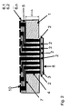
- electrodes 2 (here only one electrode 2 shown) is formed are. These can be electrically contacted via the through-hole 4 guided through the substrate 1 to the rear side, with an electrical voltage source (not illustrated).
- an electrical contact surface 9 is formed on the back with a metallization, which can be used for soldering or wire bonding or for any other means of connection.
- the further electrode 8 serves to connect to the ground potential.
- electrodes 2 are again discretely and electrically insulated from one another on a surface of the substrate 1.
- an active layer 3 of piezoelectric material which is covered with a further electrode 8, is present.
- each individual electrode 2 each have their own through-hole 4 guided to the back of the substrate 1.
- six electrically non-conductive layers 6.1 to 6.6 are formed as a multi-layer structure in this example.
- conductor tracks 7 are formed, which are electrically conductively connected by means of the plated-through holes 5 in the electrically non-conductive layers (6.1 to 6.6) with contact surfaces 10.
- strip-shaped electrodes 2 are formed on the surface of a substrate 1 in a series arrangement or line arrangement.
- the maximum possible center distance of the elements determines the maximum possible width of the individual strip-shaped electrodes (2).
- the electrodes 2 are formed with a square surface, each having the same area size and equal distances from each other.
- the maximum possible center distance of the electrodes 2 determines the maximum possible side lengths of the individual electrodes (2).
- Electrodes 2 it is also possible to use other geometric electrode surface forms than those shown here. It is also possible the size and / or the distances of electrodes 2 in a series or matrix arrangement to vary.
Priority Applications (1)
| Application Number | Priority Date | Filing Date | Title |
|---|---|---|---|
| EP09010474A EP2283935A1 (fr) | 2009-08-13 | 2009-08-13 | Système de convertisseur à ultrasons et son procédé de fonctionnement |
Applications Claiming Priority (1)
| Application Number | Priority Date | Filing Date | Title |
|---|---|---|---|
| EP09010474A EP2283935A1 (fr) | 2009-08-13 | 2009-08-13 | Système de convertisseur à ultrasons et son procédé de fonctionnement |
Publications (1)
| Publication Number | Publication Date |
|---|---|
| EP2283935A1 true EP2283935A1 (fr) | 2011-02-16 |
Family
ID=41459788
Family Applications (1)
| Application Number | Title | Priority Date | Filing Date |
|---|---|---|---|
| EP09010474A Ceased EP2283935A1 (fr) | 2009-08-13 | 2009-08-13 | Système de convertisseur à ultrasons et son procédé de fonctionnement |
Country Status (1)
| Country | Link |
|---|---|
| EP (1) | EP2283935A1 (fr) |
Cited By (2)
| Publication number | Priority date | Publication date | Assignee | Title |
|---|---|---|---|---|
| EP2631015A2 (fr) | 2012-02-24 | 2013-08-28 | Fraunhofer-Gesellschaft zur Förderung der angewandten Forschung e.V. | Convertisseur d'ultrasons destiné à l'excitation et/ou la détection de fréquences différentes d'ultrasons |
| DE102015210700A1 (de) * | 2015-06-11 | 2016-12-15 | Fraunhofer-Gesellschaft zur Förderung der angewandten Forschung e.V. | Verfahren zur Detektion von Fehlern oder Defekten an Bauteilen unter Einsatz von Ultraschallwandlern |
Citations (7)
| Publication number | Priority date | Publication date | Assignee | Title |
|---|---|---|---|---|
| WO1996025244A1 (fr) * | 1995-02-16 | 1996-08-22 | Precision Acoustics Limited | Couplage electrique pour detecteur piezo-electrique a ultrasons |
| WO2003000337A2 (fr) * | 2001-06-20 | 2003-01-03 | Bae Systems Information And Electronic Systems Integration Inc | Ensemble reseau a ultrasons piezocomposite et circuit integre presentant des caracteristiques d'expansion thermique et diaphoniques acoustiques ameliorees |
| US20030028108A1 (en) * | 2001-07-31 | 2003-02-06 | Miller David G. | System for attaching an acoustic element to an integrated circuit |
| JP2003079621A (ja) * | 2001-09-14 | 2003-03-18 | Toshiba Corp | 超音波プローブおよび超音波診断装置 |
| US20030102777A1 (en) * | 2001-12-05 | 2003-06-05 | Fuji Photo Film Co., Ltd. | Ultrasonic transducer and method of manufacturing the same |
| US20030205947A1 (en) * | 2002-05-01 | 2003-11-06 | Klee Mareike Katharine | Ultrasonic membrane transducer for an ultrasonic diagnostic probe |
| JP2006122105A (ja) * | 2004-10-26 | 2006-05-18 | Toshiba Corp | 超音波プローブ |
-
2009
- 2009-08-13 EP EP09010474A patent/EP2283935A1/fr not_active Ceased
Patent Citations (8)
| Publication number | Priority date | Publication date | Assignee | Title |
|---|---|---|---|---|
| WO1996025244A1 (fr) * | 1995-02-16 | 1996-08-22 | Precision Acoustics Limited | Couplage electrique pour detecteur piezo-electrique a ultrasons |
| WO2003000337A2 (fr) * | 2001-06-20 | 2003-01-03 | Bae Systems Information And Electronic Systems Integration Inc | Ensemble reseau a ultrasons piezocomposite et circuit integre presentant des caracteristiques d'expansion thermique et diaphoniques acoustiques ameliorees |
| US20030013969A1 (en) * | 2001-06-20 | 2003-01-16 | Erikson Kenneth R. | Acoustical array with multilayer substrate integrated circuits |
| US20030028108A1 (en) * | 2001-07-31 | 2003-02-06 | Miller David G. | System for attaching an acoustic element to an integrated circuit |
| JP2003079621A (ja) * | 2001-09-14 | 2003-03-18 | Toshiba Corp | 超音波プローブおよび超音波診断装置 |
| US20030102777A1 (en) * | 2001-12-05 | 2003-06-05 | Fuji Photo Film Co., Ltd. | Ultrasonic transducer and method of manufacturing the same |
| US20030205947A1 (en) * | 2002-05-01 | 2003-11-06 | Klee Mareike Katharine | Ultrasonic membrane transducer for an ultrasonic diagnostic probe |
| JP2006122105A (ja) * | 2004-10-26 | 2006-05-18 | Toshiba Corp | 超音波プローブ |
Non-Patent Citations (1)
| Title |
|---|
| YUAN YI-QUAN ET AL: "PVDF-DMOS SENSORS AND ARRAY FOR UNDERWATER ACOUSTIC IMAGING", ACOUSTICAL IMAGING. SENDAI, MAY 31 - JUNE 2, 1988; [PROCEEDINGS OF THE INTERNATIONAL SYMPOSIUM ACOUSTICAL IMAGING], vol. VOL. 17, 31 May 1988 (1988-05-31) - 2 June 1988 (1988-06-02), pages 609 - 617, XP000044002 * |
Cited By (6)
| Publication number | Priority date | Publication date | Assignee | Title |
|---|---|---|---|---|
| EP2631015A2 (fr) | 2012-02-24 | 2013-08-28 | Fraunhofer-Gesellschaft zur Förderung der angewandten Forschung e.V. | Convertisseur d'ultrasons destiné à l'excitation et/ou la détection de fréquences différentes d'ultrasons |
| DE102012003495A1 (de) | 2012-02-24 | 2013-08-29 | Fraunhofer-Gesellschaft zur Förderung der angewandten Forschung e.V. | Ultraschallwandler zur Anregung und/oder zur Detektion von Ultraschall unterschiedlicher Frequenzen |
| DE102012003495B4 (de) * | 2012-02-24 | 2015-04-09 | Fraunhofer-Gesellschaft zur Förderung der angewandten Forschung e.V. | Ultraschallwandler zur Anregung und/oder zur Detektion von Ultraschall unterschiedlicher Frequenzen |
| EP2631015A3 (fr) * | 2012-02-24 | 2016-08-24 | Fraunhofer-Gesellschaft zur Förderung der angewandten Forschung e.V. | Convertisseur d'ultrasons destiné à l'excitation et/ou la détection de fréquences différentes d'ultrasons |
| DE102015210700A1 (de) * | 2015-06-11 | 2016-12-15 | Fraunhofer-Gesellschaft zur Förderung der angewandten Forschung e.V. | Verfahren zur Detektion von Fehlern oder Defekten an Bauteilen unter Einsatz von Ultraschallwandlern |
| DE102015210700B4 (de) | 2015-06-11 | 2023-11-09 | Fraunhofer-Gesellschaft zur Förderung der angewandten Forschung e.V. | Verfahren zur Detektion von Fehlern oder Defekten an Bauteilen unter Einsatz von Ultraschallwandlern |
Similar Documents
| Publication | Publication Date | Title |
|---|---|---|
| DE102005053767B4 (de) | MEMS-Mikrofon, Verfahren zur Herstellung und Verfahren zum Einbau | |
| US5655276A (en) | Method of manufacturing two-dimensional array ultrasonic transducers | |
| US5091893A (en) | Ultrasonic array with a high density of electrical connections | |
| US7148608B2 (en) | Multi-layer ceramic acoustic transducer | |
| KR100722370B1 (ko) | 적층형 초음파 탐촉자 및 이의 제조방법 | |
| WO2005107962A1 (fr) | Transducteur d'ultrasons et son procede de fabrication | |
| JP4758634B2 (ja) | 多層セラミック音響変換器の製造方法 | |
| DE10151125A1 (de) | Anschlussstruktur und zugehöriges Herstellungsverfahren sowie die Anschlussstruktur verwendende Prüfanschlussanordnung | |
| TW201109668A (en) | Inspection socket | |
| US20060154075A1 (en) | Multilayered structure and method of manufacturing the same, and ultrasonic transducer | |
| DE102012003495B4 (de) | Ultraschallwandler zur Anregung und/oder zur Detektion von Ultraschall unterschiedlicher Frequenzen | |
| EP2288912B1 (fr) | Agencement d'un résonateur piézoacoustique sur un miroir acoustique d'un substrat, procédé pour produire un tel agencement et utilisation de ce dernier | |
| DE102011083627A1 (de) | Verfahren zur Kontaktierung eines elektronischen Bauteils und Baugruppe mit einem elektronischen Bauteil auf einem Substrat | |
| WO2010006849A2 (fr) | Procédé de réalisation d'un composant, procédé de réalisation d'un système de composants, composant et système de composants correspondants | |
| EP0166180B1 (fr) | Hydrophone | |
| WO2008135004A1 (fr) | Batterie de transducteurs ultrasonores pour applications dans des fluides gazeux | |
| EP2283935A1 (fr) | Système de convertisseur à ultrasons et son procédé de fonctionnement | |
| EP2817259B1 (fr) | Procédé de fabrication d'un capteur | |
| DE102013110900B4 (de) | Prüfkopf für luftgekoppelten Ultraschall | |
| EP1989731B1 (fr) | Procédé de fabrication et de mise en contact planaire d'un dispositif électronique | |
| JP2022552082A (ja) | 音響トランスデューサ及び製造方法 | |
| Decharat et al. | High frequency copolymer ultrasonic transducer array of size-effective elements | |
| DE10018355A1 (de) | Ultraschallwandler und Verfahren zur Herstellung eines Ultraschallwandlers | |
| US10553779B2 (en) | Method of fabricating an acoustic transducer | |
| DE3019410A1 (de) | Verfahren zum herstellen einer ultraschallwandleranordnung |
Legal Events
| Date | Code | Title | Description |
|---|---|---|---|
| PUAI | Public reference made under article 153(3) epc to a published international application that has entered the european phase |
Free format text: ORIGINAL CODE: 0009012 |
|
| AK | Designated contracting states |
Kind code of ref document: A1 Designated state(s): AT BE BG CH CY CZ DE DK EE ES FI FR GB GR HR HU IE IS IT LI LT LU LV MC MK MT NL NO PL PT RO SE SI SK SM TR |
|
| AX | Request for extension of the european patent |
Extension state: AL BA RS |
|
| 17P | Request for examination filed |
Effective date: 20110815 |
|
| 17Q | First examination report despatched |
Effective date: 20141021 |
|
| STAA | Information on the status of an ep patent application or granted ep patent |
Free format text: STATUS: EXAMINATION IS IN PROGRESS |
|
| STAA | Information on the status of an ep patent application or granted ep patent |
Free format text: STATUS: THE APPLICATION HAS BEEN REFUSED |
|
| 18R | Application refused |
Effective date: 20200808 |