EP2283935A1 - Ultrasound converter system and method for its operation - Google Patents
Ultrasound converter system and method for its operation Download PDFInfo
- Publication number
- EP2283935A1 EP2283935A1 EP09010474A EP09010474A EP2283935A1 EP 2283935 A1 EP2283935 A1 EP 2283935A1 EP 09010474 A EP09010474 A EP 09010474A EP 09010474 A EP09010474 A EP 09010474A EP 2283935 A1 EP2283935 A1 EP 2283935A1
- Authority
- EP
- European Patent Office
- Prior art keywords
- electrodes
- substrate
- active layer
- electrically
- emitted
- Prior art date
- Legal status (The legal status is an assumption and is not a legal conclusion. Google has not performed a legal analysis and makes no representation as to the accuracy of the status listed.)
- Ceased
Links
- 238000000034 method Methods 0.000 title claims abstract description 11
- 238000002604 ultrasonography Methods 0.000 title description 7
- 239000000758 substrate Substances 0.000 claims abstract description 38
- 239000000463 material Substances 0.000 claims abstract description 17
- 239000004020 conductor Substances 0.000 claims description 6
- 239000011159 matrix material Substances 0.000 claims description 6
- 239000010409 thin film Substances 0.000 claims description 3
- 239000010931 gold Substances 0.000 description 4
- 230000004913 activation Effects 0.000 description 3
- 229910052737 gold Inorganic materials 0.000 description 3
- 238000004519 manufacturing process Methods 0.000 description 3
- 238000005476 soldering Methods 0.000 description 3
- 239000000853 adhesive Substances 0.000 description 2
- 238000004026 adhesive bonding Methods 0.000 description 2
- 230000001070 adhesive effect Effects 0.000 description 2
- 239000000919 ceramic Substances 0.000 description 2
- 230000008878 coupling Effects 0.000 description 2
- 238000010168 coupling process Methods 0.000 description 2
- 238000005859 coupling reaction Methods 0.000 description 2
- 230000007547 defect Effects 0.000 description 2
- 238000001514 detection method Methods 0.000 description 2
- 238000005259 measurement Methods 0.000 description 2
- 229910052751 metal Inorganic materials 0.000 description 2
- 239000002184 metal Substances 0.000 description 2
- 238000001465 metallisation Methods 0.000 description 2
- 238000009659 non-destructive testing Methods 0.000 description 2
- 238000005240 physical vapour deposition Methods 0.000 description 2
- 238000001020 plasma etching Methods 0.000 description 2
- BASFCYQUMIYNBI-UHFFFAOYSA-N platinum Chemical compound [Pt] BASFCYQUMIYNBI-UHFFFAOYSA-N 0.000 description 2
- RYGMFSIKBFXOCR-UHFFFAOYSA-N Copper Chemical compound [Cu] RYGMFSIKBFXOCR-UHFFFAOYSA-N 0.000 description 1
- 239000011149 active material Substances 0.000 description 1
- 229910052782 aluminium Inorganic materials 0.000 description 1
- XAGFODPZIPBFFR-UHFFFAOYSA-N aluminium Chemical compound [Al] XAGFODPZIPBFFR-UHFFFAOYSA-N 0.000 description 1
- 230000015572 biosynthetic process Effects 0.000 description 1
- 238000004364 calculation method Methods 0.000 description 1
- 229910052802 copper Inorganic materials 0.000 description 1
- 239000010949 copper Substances 0.000 description 1
- PMHQVHHXPFUNSP-UHFFFAOYSA-M copper(1+);methylsulfanylmethane;bromide Chemical compound Br[Cu].CSC PMHQVHHXPFUNSP-UHFFFAOYSA-M 0.000 description 1
- 230000007423 decrease Effects 0.000 description 1
- 238000000708 deep reactive-ion etching Methods 0.000 description 1
- 230000032798 delamination Effects 0.000 description 1
- 238000011161 development Methods 0.000 description 1
- 230000018109 developmental process Effects 0.000 description 1
- 238000005516 engineering process Methods 0.000 description 1
- 238000005530 etching Methods 0.000 description 1
- 239000011521 glass Substances 0.000 description 1
- PCHJSUWPFVWCPO-UHFFFAOYSA-N gold Chemical compound [Au] PCHJSUWPFVWCPO-UHFFFAOYSA-N 0.000 description 1
- 238000000608 laser ablation Methods 0.000 description 1
- 150000002739 metals Chemical class 0.000 description 1
- 229910021421 monocrystalline silicon Inorganic materials 0.000 description 1
- 150000004767 nitrides Chemical class 0.000 description 1
- 230000010363 phase shift Effects 0.000 description 1
- 229910052697 platinum Inorganic materials 0.000 description 1
- 229920000642 polymer Polymers 0.000 description 1
- 238000007650 screen-printing Methods 0.000 description 1
- 239000004065 semiconductor Substances 0.000 description 1
- 238000007740 vapor deposition Methods 0.000 description 1
- 238000003631 wet chemical etching Methods 0.000 description 1
Images


Classifications
-
- B—PERFORMING OPERATIONS; TRANSPORTING
- B06—GENERATING OR TRANSMITTING MECHANICAL VIBRATIONS IN GENERAL
- B06B—METHODS OR APPARATUS FOR GENERATING OR TRANSMITTING MECHANICAL VIBRATIONS OF INFRASONIC, SONIC, OR ULTRASONIC FREQUENCY, e.g. FOR PERFORMING MECHANICAL WORK IN GENERAL
- B06B1/00—Methods or apparatus for generating mechanical vibrations of infrasonic, sonic, or ultrasonic frequency
- B06B1/02—Methods or apparatus for generating mechanical vibrations of infrasonic, sonic, or ultrasonic frequency making use of electrical energy
- B06B1/06—Methods or apparatus for generating mechanical vibrations of infrasonic, sonic, or ultrasonic frequency making use of electrical energy operating with piezoelectric effect or with electrostriction
- B06B1/0607—Methods or apparatus for generating mechanical vibrations of infrasonic, sonic, or ultrasonic frequency making use of electrical energy operating with piezoelectric effect or with electrostriction using multiple elements
- B06B1/0622—Methods or apparatus for generating mechanical vibrations of infrasonic, sonic, or ultrasonic frequency making use of electrical energy operating with piezoelectric effect or with electrostriction using multiple elements on one surface
Definitions
- the invention relates to an ultrasonic transducer system and method for its operation.
- ultrasonic waves with very high frequencies can be emitted and used, for example, for the non-destructive testing of workpieces or components.
- This allows a resolution in the range of 10 microns can be achieved, so that even very small reflectors, such. Defects, cracks, voids or delaminations are detectable.
- An inventive ultrasonic transducer system is designed so that on a surface of an electrically insulating or semiconductive substrate Discrete formed to each other electrodes are formed as a metallic thin film.
- each electrode is individually connected to a voltage source via an electrically conductive through-hole guided through the substrate.
- At least one active layer formed of a piezoelectric material is formed on the surface of the substrate on which these electrodes are formed. This one or more active layer (s) is / are then electrically connected to at least one further electrode and thus to the other pole of the high-frequency voltage source or the ground contact.
- an active layer assigned to the respective electrode or a surface area of an active layer can be excited with the electrodes present directly on the surface of the substrate, which are each individually electrically controllable, in order to emit ultrasonic waves from this position.
- control can take place such that a time offset by a specific phase shift, in which electrical voltage is applied to the active layer via these electrodes and an electric current flows, influences the direction with which ultrasonic waves are emitted from the respective position. be achieved.
- the piezoelectric active material is excited to high-frequency mechanical vibrations, which have then been placed as ultrasonic waves, possibly after coupling into a body on the system is, spread.
- the activation of the individual discretely arranged electrodes can be carried out in such a way that the sound waves emitted in each case by these surface regions on which the electrodes are arranged can be influenced in a targeted manner. If electrodes arranged on the outer edge are actuated offset in time from the electrodes arranged successively further inwardly, a focused acoustic emission is possible. However, it is also possible to achieve a sound emission directed at a certain angle, deviating from 90 ° to the surface of the active layer (s), by a subsequent subsequent activation of electrodes.
- the center distance of discrete juxtaposed electrodes should be less than half the wavelength of the sound waves in a material or body into which the sound waves are emitted.
- the wavelength depends on the speed of sound in the material and the frequency of the sound waves. The wavelength decreases with increasing frequency. This also requires miniaturization of the ultrasonic transducers, which can be achieved with a system according to the invention and the advantageous electrical contacting, even with conventional connection techniques.
- Electrodes can form a series, line, ring or matrix arrangement.
- the respective arrangement spatially limits the possible acoustic emission.
- the influencing of the sound emission direction can take place only in one spatial plane.
- matrix or ring arrangements a three-dimensional full influence can be achieved.
- Ultrasonic transducers are also commonly used for testing and diagnostic purposes.
- the emitted ultrasonic waves are reflected in an adjacent material or material at defects, interfaces or the back of a body to be tested.
- a part of the reflected sound waves again hits the respective ultrasonic transducer.
- the sound pressure of these reflected sound waves causes mechanical deformation of the piezoelectric layer, which are converted by the layer into correspondingly proportional electrical voltage signals.
- the contact surfaces may form a widened connection structure in which these contact surfaces are distributed on a surface that is larger than the area of the active layer (s) on the front side of the substrate.
- Various materials for the substrates can be used for the production of systems according to the invention. These may be, for example, semiconductor materials (preferably monocrystalline silicon), ceramics, glass or polymers.
- the electrodes on the surface of the substrate can be applied as metallic thin films.
- the structuring can be carried out by known methods additively (via change masks or adhesive masks) or subtractive (etching).
- Suitable metals are copper, gold, aluminum, platinum or multilayer systems, such as e.g. a Cr-Au, Ni-Au or Ti-Cu-Au. There should be good adhesion to the substrate and the active layer (s).
- any desired piezoelectric materials such as AlN, ZnO or PZT can be used. Again, an order can be made by physical vapor deposition.
- the openings can be formed by reactive ion etching (DRIE), plasma etching, wet-chemical etching or by laser ablation. After the formation of the openings whose inner walls can be metallized and / or filled with an electrically conductive material.
- the metallization can be applied by physical vapor deposition, which can be galvanically enhanced if necessary.
- Filling with an electrically conductive material can also be done with such a vapor deposition, but also by screen printing.
- a metal or an electrically conductive polymeric material can be introduced in openings.
- electrically non-conductive layers can also be applied as thin layers to the substrate. These may be, for example, suitable oxide or nitride layers. Through-connections may also be present in the electrically non-conductive layers with which the conductor tracks in the different planes can be electrically conductively connected.
- conventional multilayer substrates for example printed circuit boards, ceramic multilayer circuits
- interconnect structures can also be used for this purpose.
- an active layer covers all electrodes formed on the surface of the substrate.
- each electrode can also be assigned its own active layer be. At least the electrodes should be designed so that no electrical current flow from one electrode to another electrode is possible.
- the total thickness of the substrate including the plated-through wiring planes, would be significantly greater than the wavelength of the ultrasound in the substrate. Since the piezoelectric material vibrates mechanically in both directions, the backward emitted sound waves should be absorbed in the substrate. Possible reflections in the substrate material should not hit the piezoelectric active layer again in order to avoid undesired interference signals.
- the individual electrodes formed on the substrate surface should, depending on the selected geometric configuration, have a width which is smaller than the wavelength of the sound waves in a material into which the sound waves are emitted.
- the further electrode (s) may be formed on an active layer. This then forms, at least in some areas, the surface of the element from which ultrasonic waves are emitted.
- a pulsed electrical voltage is applied to the electrodes.
- there is a single pulse which can be carried out repeatedly with time interruptions. In periods when no sound waves are emitted, a detection of reflected sound waves can take place.
- ultrasound can be emitted and detected at frequencies of at least 30 MHz.
- the electrically conductive connections of the system for connection to a voltage source can be realized at the contact surfaces in an expanded arrangement at the rear side of the substrate with known technologies. This can e.g. by soldering, wire bonding or gluing (e.g., with electrically conductive adhesive).
- the ultrasonic transducer systems according to the invention achieve both a higher lateral and a low resolution in the micrometer range.
- New areas of application such as an effective nondestructive testing in electronics manufacturing, can be developed.
- electrodes 2 (here only one electrode 2 shown) is formed are. These can be electrically contacted via the through-hole 4 guided through the substrate 1 to the rear side, with an electrical voltage source (not illustrated).
- an electrical contact surface 9 is formed on the back with a metallization, which can be used for soldering or wire bonding or for any other means of connection.
- the further electrode 8 serves to connect to the ground potential.
- electrodes 2 are again discretely and electrically insulated from one another on a surface of the substrate 1.
- an active layer 3 of piezoelectric material which is covered with a further electrode 8, is present.
- each individual electrode 2 each have their own through-hole 4 guided to the back of the substrate 1.
- six electrically non-conductive layers 6.1 to 6.6 are formed as a multi-layer structure in this example.
- conductor tracks 7 are formed, which are electrically conductively connected by means of the plated-through holes 5 in the electrically non-conductive layers (6.1 to 6.6) with contact surfaces 10.
- strip-shaped electrodes 2 are formed on the surface of a substrate 1 in a series arrangement or line arrangement.
- the maximum possible center distance of the elements determines the maximum possible width of the individual strip-shaped electrodes (2).
- the electrodes 2 are formed with a square surface, each having the same area size and equal distances from each other.
- the maximum possible center distance of the electrodes 2 determines the maximum possible side lengths of the individual electrodes (2).
- Electrodes 2 it is also possible to use other geometric electrode surface forms than those shown here. It is also possible the size and / or the distances of electrodes 2 in a series or matrix arrangement to vary.
Abstract
Description
Die Erfindung betrifft ein Ultraschallwandlersystem und Verfahren zu dessen Betrieb. Dabei können insbesondere Ultraschallwellen mit sehr hohen Frequenzen emittiert und beispielsweise für die zerstörungsfreie Prüfung von Werkstücken oder Bauteilen genutzt werden. Dadurch kann eine Auflösung im Bereich von 10 µm erreicht werden, so dass auch sehr kleine Reflektoren, wie z.B. Defekte, Risse, Lunker oder Delaminationen detektierbar sind.The invention relates to an ultrasonic transducer system and method for its operation. In particular, ultrasonic waves with very high frequencies can be emitted and used, for example, for the non-destructive testing of workpieces or components. This allows a resolution in the range of 10 microns can be achieved, so that even very small reflectors, such. Defects, cracks, voids or delaminations are detectable.
Da mit der Erfindung auch sehr kleine Strukturen detektiert werden sollen, ist eine hohe Auflösung erforderlich, die nur durch Einsatz von Ultraschall mit sehr hohen Frequenzen möglich ist. Häufig wird auch ein Einsatz von Ultraschallwandlern gefordert, bei dem Strukturen ortsaufgelöst im Volumen von Körpern erkannt werden sollen und der Ultraschallwandler nicht auf die Oberfläche des Körpers aufgesetzt und über seine Oberfläche bewegt werden soll. Dies erfordert eine gezielte Beeinflussung der Richtung in der Schallwellen vom Ultraschallwandler emittiert werden sollen. Es ist seit jüngster Vergangenheit üblich, für solche Anwendungen Mehrelementultraschallwandler einzusetzen.Since very small structures are to be detected with the invention, a high resolution is required, which is only possible by using ultrasound at very high frequencies. Frequently, an application of ultrasonic transducers is required in which structures are to be detected spatially resolved in the volume of bodies and the ultrasonic transducer should not be placed on the surface of the body and moved over its surface. This requires a targeted influencing of the direction in which sound waves are to be emitted by the ultrasound transducer. It has been common in recent years to use multi-element ultrasound transducers for such applications.
Da Ultraschall mit einer sehr hohen Frequenz eingesetzt werden sollen, ist eine Miniaturisierung erforderlich. Dabei ist es auch beachtsam, dass eine gezielte Emissionsrichtung von emittierten Schallwellen häufig gefordert wird. Bei den Frequenzen im mittleren bis oberen Megaherzbereich ist auch eine hohe Auflösung, also eine sehr kleine Fläche erforderlich, von der Ultraschallwellen emittiert werden müssen. Dies ist aber für die Führung der elektrischen Zuleitungen zu berücksichtigen.Since ultrasound is to be used at a very high frequency, miniaturization is required. It is also noteworthy that a targeted emission direction of emitted sound waves is often required. The frequencies in the middle to upper megahertz range also require a high resolution, ie a very small area, from which ultrasonic waves have to be emitted. But this is to be considered for the guidance of the electrical leads.
Es ist daher Aufgabe der Erfindung, Möglichkeiten vorzuschlagen mit denen Ultraschallwellen mit erhöhter Frequenz und hoher Auflösung in unterschiedliche Richtungen emittiert und wieder detektiert werden können.It is therefore an object of the invention to propose ways in which ultrasonic waves with increased frequency and high resolution can be emitted in different directions and detected again.
Erfindungsgemäß wird diese Aufgabe mit einem Ultraschallwandlersystem, das die Merkmale des Anspruchs 1 aufweist, gelöst. Es kann mit einem Verfahren nach Anspruch 9 betrieben werden. Vorteilhafte Ausgestaltungen und Weiterbildungen der Erfindung können mit in untergeordneten Ansprüchen bezeichneten Merkmalen realisiert werden.According to the invention, this object is achieved with an ultrasonic transducer system having the features of
Ein erfindungsgemäßes Ultraschallwandlersystem ist dabei so ausgebildet, dass an einer Oberfläche eines elektrisch isolierenden oder halbleitenden Substrats diskret zueinander ausgebildete Elektroden, als metallische Dünnschicht ausgebildet sind. Dabei ist jede Elektrode einzeln über eine elektrisch leitende durch das Substrat hindurch geführte Durchkontaktierung mit einer Spannungsquelle verbunden.An inventive ultrasonic transducer system is designed so that on a surface of an electrically insulating or semiconductive substrate Discrete formed to each other electrodes are formed as a metallic thin film. In this case, each electrode is individually connected to a voltage source via an electrically conductive through-hole guided through the substrate.
Auf der Oberfläche des Substrates an der diese Elektroden ausgebildet sind, ist mindestens eine aus einem piezoelektrischen Material/Stoff gebildete aktive Schicht ausgebildet. Diese eine aktive oder mehrere aktive Schicht(en) ist/sind dann mit mindestens einer weiteren Elektrode und damit mit dem anderen Pol der Hochfrequenzspannungsquelle oder dem Massekontakt elektrisch leitend verbunden.On the surface of the substrate on which these electrodes are formed, at least one active layer formed of a piezoelectric material is formed. This one or more active layer (s) is / are then electrically connected to at least one further electrode and thus to the other pole of the high-frequency voltage source or the ground contact.
Dadurch kann mit den unmittelbar an der Oberfläche des Substrats vorhandenen Elektroden, die jeweils einzeln elektrisch ansteuerbar sind, eine der jeweiligen Elektrode zugeordnete aktive Schicht oder ein Flächenbereich einer aktiven Schicht angeregt werden, um von dieser Position Ultraschallwellen zu emittieren.As a result, an active layer assigned to the respective electrode or a surface area of an active layer can be excited with the electrodes present directly on the surface of the substrate, which are each individually electrically controllable, in order to emit ultrasonic waves from this position.
Dabei kann die Ansteuerung so erfolgen, dass ein Zeitversatz durch eine gezielte Phasenverschiebung, bei der über diese Elektroden elektrische Spannung an die aktive Schicht angelegt wird und dabei ein elektrischer Strom fließt, eine Beeinflussung der Richtung, mit der Ultraschallwellen von der jeweiligen Position emittiert werden, erreicht werden.In this case, the control can take place such that a time offset by a specific phase shift, in which electrical voltage is applied to the active layer via these electrodes and an electric current flows, influences the direction with which ultrasonic waves are emitted from the respective position. be achieved.
Durch das Anlegen einer elektrischen Spannung wird das piezoelektrische aktive Material zu hochfrequenten mechanischen Schwingungen angeregt, die sich dann als Ultraschallwellen ggf. nach einer Einkopplung in einen Körper auf den das System aufgesetzt worden ist, ausbreiten. Dabei kann die Ansteuerung der einzelnen diskret zueinander angeordneten Elektroden so erfolgen, dass die jeweils von diesen Flächenbereichen, an denen die Elektroden angeordnet sind, emittierten Schallwellen gezielt beeinflusst werden können. Werden am äußeren Rand angeordnete Elektroden zeitlich versetzt vor den sukzessive weiter innen liegend angeordneten Elektroden angesteuert, ist eine fokussierte Schallemission möglich. Es besteht aber auch die Möglichkeit, durch eine zeitlich nachfolgende Ansteuerung von Elektroden eine in einem bestimmten Winkel, abweichend von 90° zur Oberfläche der aktiven Schicht(en), ausgerichtete Schallemission zu erreichen.By applying an electrical voltage, the piezoelectric active material is excited to high-frequency mechanical vibrations, which have then been placed as ultrasonic waves, possibly after coupling into a body on the system is, spread. In this case, the activation of the individual discretely arranged electrodes can be carried out in such a way that the sound waves emitted in each case by these surface regions on which the electrodes are arranged can be influenced in a targeted manner. If electrodes arranged on the outer edge are actuated offset in time from the electrodes arranged successively further inwardly, a focused acoustic emission is possible. However, it is also possible to achieve a sound emission directed at a certain angle, deviating from 90 ° to the surface of the active layer (s), by a subsequent subsequent activation of electrodes.
Durch eine zeitverzögerte Ansteuerung der Elektroden kann auf die jeweilige Richtung der von dort emittierten Schallwellen Einfluss genommen werden, da sich die einzelnen im Flächenbereich von Elektroden emittierten Schallwellen zu einer resultierenden Wellenfront in einer bestimmten Richtung überlagern. Zur Emission von Schallwellen mit möglichst großen Winkeln, sollte der Mittenabstand von diskret nebeneinander angeordneten Elektroden kleiner als die halbe Wellenlänge der Schallwellen in einem Werkstoff oder Körper, in den die Schallwellen emittiert werden, sein. Die Wellenlänge ist dabei von der Schallgeschwindigkeit im Werkstoff und der Frequenz der Schallwellen abhängig. Die Wellenlänge verkleinert sich dabei mit größer werdender Frequenz. Dies erfordert auch eine Miniaturisierung der Ultraschallwandler, was mit einem erfindungsgemäßen System und die vorteilhafte elektrische Kontaktierung, auch mit konventionellen Verbindungstechniken, erreichbar ist.By a time-delayed activation of the electrodes, it is possible to influence the respective direction of the sound waves emitted there, since the individual sound waves emitted in the area of electrodes are superimposed in a specific direction to form a resulting wavefront. For the emission of sound waves with the largest possible angles, the center distance of discrete juxtaposed electrodes should be less than half the wavelength of the sound waves in a material or body into which the sound waves are emitted. The wavelength depends on the speed of sound in the material and the frequency of the sound waves. The wavelength decreases with increasing frequency. This also requires miniaturization of the ultrasonic transducers, which can be achieved with a system according to the invention and the advantageous electrical contacting, even with conventional connection techniques.
Die auf der Oberfläche des Substrates angeordneten Elektroden können eine Reihen-, Linien-, Ring- oder Matrixanordnung bilden. Die jeweilige Anordnung grenzt die damit mögliche Schallemission räumlich ein. Bei einer Reihen- oder Linienanordnung kann beispielsweise die Beeinflussung der Schallemissionsrichtung nur in einer Raumebene erfolgen. Bei Matrix-oder Ringanordnungen kann eine dreidimensionale vollständige Beeinflussung erreicht werden.The arranged on the surface of the substrate Electrodes can form a series, line, ring or matrix arrangement. The respective arrangement spatially limits the possible acoustic emission. In the case of a series or line arrangement, for example, the influencing of the sound emission direction can take place only in one spatial plane. In matrix or ring arrangements, a three-dimensional full influence can be achieved.
Ultraschallwandler werden üblicherweise auch zu Prüfund Diagnosezwecken eingesetzt. Die emittierten Ultraschallwellen werden in einem angrenzenden Werkstoff oder Material an Defekten, Grenzflächen oder der Rückseite eines zu prüfenden Körpers reflektiert. Ein Teil der reflektierten Schallwellen trifft wieder auf den jeweiligen Ultraschallwandler auf. Der Schalldruck dieser reflektierten Schallwellen bewirkt mechanische Verformungen der piezoelektrischen Schicht, die von der Schicht in dementsprechend proportionale elektrische Spannungssignale umgewandelt werden. Über eine Auswertung der Amplituden und der Zeitverläufe der einzelnen so erfassten Messsignale, kann eine ortsaufgelöste Abbildung der inneren Struktur eines untersuchten Körpers durch Berechnung rekonstruiert werden.Ultrasonic transducers are also commonly used for testing and diagnostic purposes. The emitted ultrasonic waves are reflected in an adjacent material or material at defects, interfaces or the back of a body to be tested. A part of the reflected sound waves again hits the respective ultrasonic transducer. The sound pressure of these reflected sound waves causes mechanical deformation of the piezoelectric layer, which are converted by the layer into correspondingly proportional electrical voltage signals. By evaluating the amplitudes and the time profiles of the individual measurement signals thus acquired, a spatially resolved image of the internal structure of an examined body can be reconstructed by calculation.
Insbesondere wegen der erforderlichen Miniaturisierung, ist es vorteilhaft, die große Anzahl an elektrisch leitenden Verbindungen zu den Elektroden mittels Durchkontaktierungen (Via's) auszubilden. Diese können dabei, wie bereits erwähnt, durch das Substrat hindurchgeführt werden. Zusätzlich können aber weitere Durchkontaktierungen genutzt werden, die als elektrisch leitende Verbindungen durch eine oder mehrere elektrisch nicht leitende(n) Schicht(en) geführt sind. Diese Schicht(en) kann/können auf der Rückseite des Substrates, also auf der Seite, die der Seite auf der die Elektroden ausgebildet sind, gegenüberliegt, angeordnet sein. Zwischen oder auf diesen Schichten können elektrische Leiterbahnen, die zu einer Aufweitung von an der Rückseite angeordneten Kontaktflächen genutzt werden können, vorhanden sein. Auf der nach außen weisenden elektrisch nicht leitenden Schicht können die Kontaktflächen eine aufgeweitete Anschlussstruktur bilden, bei der diese Kontaktflächen auf einer Fläche verteilt angeordnet sind, die größer als die Fläche der aktiven Schicht(en) auf der Vorderseite des Substrates ist. Dadurch ist eine elektrische Kontaktierung mit konventionellen Verbindungstechniken, wie Löten, Drahtbonden oder Kleben möglich.In particular, because of the required miniaturization, it is advantageous to form the large number of electrically conductive connections to the electrodes by means of vias (via's). These can, as already mentioned, be passed through the substrate. In addition, however, further plated-through holes can be used, which are guided as electrically conductive connections through one or more electrically nonconductive layer (s). This layer (s) can be on the back of the substrate, that is, on the side opposite to the side on which the electrodes are formed. Between or on these layers, electrical conductor tracks, which can be used to widen contact surfaces arranged on the rear side, may be present. On the outwardly facing electrically non-conductive layer, the contact surfaces may form a widened connection structure in which these contact surfaces are distributed on a surface that is larger than the area of the active layer (s) on the front side of the substrate. As a result, an electrical contact with conventional connection techniques, such as soldering, wire bonding or gluing is possible.
Für die Herstellung erfindungsgemäßer Systeme können verschiedene Werkstoffe für die Substrate eingesetzt werden. Dies können beispielsweise Halbleiterwerkstoffe (bevorzugt einkristallines Silicium), Keramiken, Glas oder Polymere sein.Various materials for the substrates can be used for the production of systems according to the invention. These may be, for example, semiconductor materials (preferably monocrystalline silicon), ceramics, glass or polymers.
Die Elektroden auf der Oberfläche des Substrates können als metallische Dünnschichten aufgebracht werden. Die Strukturierung kann mit bekannten Verfahren additiv (über Wechselmasken oder Haftmasken) oder subtraktiv (Ätzen) erfolgen. Geeignete Metalle sind Kupfer, Gold, Aluminium, Platin oder Mehrschichtsysteme, wie z.B. eine Cr-Au, Ni-Au oder Ti-Cu-Au. Es sollte eine gute Haftung am Substrat und der aktiven Schicht(en) gegeben sein.The electrodes on the surface of the substrate can be applied as metallic thin films. The structuring can be carried out by known methods additively (via change masks or adhesive masks) or subtractive (etching). Suitable metals are copper, gold, aluminum, platinum or multilayer systems, such as e.g. a Cr-Au, Ni-Au or Ti-Cu-Au. There should be good adhesion to the substrate and the active layer (s).
Für die aktive(n) Schicht(en) können an sich beliebige piezoelektrische Materialien, wie AlN, ZnO oder PZT eingesetzt werden. Auch hier kann ein Auftrag mittels physikalischer Gasphasenabscheidung erfolgen. Für die Herstellung der Durchkontaktierungen durch ein Substrat können die Durchbrechungen durch reaktives Ionenätzen (DRIE), Plasmaätzen, nasschemisches Ätzen oder mittels Laserabtrag ausgebildet werden. Nach der Ausbildung der Durchbrechungen können deren Innenwände metallisiert und/oder mit einem elektrisch leitfähigem Material gefüllt werden. Die Metallisierung kann durch physikalische Gasphasenabscheidung aufgebracht werden, die ggf. galvanisch verstärkt werden kann.For the active layer (s), any desired piezoelectric materials such as AlN, ZnO or PZT can be used. Again, an order can be made by physical vapor deposition. For the production of the plated-through holes through a substrate, the openings can be formed by reactive ion etching (DRIE), plasma etching, wet-chemical etching or by laser ablation. After the formation of the openings whose inner walls can be metallized and / or filled with an electrically conductive material. The metallization can be applied by physical vapor deposition, which can be galvanically enhanced if necessary.
Ein Ausfüllen mit einem elektrisch leitenden Material kann ebenfalls mit einer solchen Gasphasenabscheidung, aber auch durch Siebdruck erfolgen. Dabei kann ein Metall oder auch ein elektrisch leitfähiges polymeres Material in Durchbrechungen eingebracht werden.Filling with an electrically conductive material can also be done with such a vapor deposition, but also by screen printing. In this case, a metal or an electrically conductive polymeric material can be introduced in openings.
Die bereits erwähnten elektrisch nicht leitenden Schichten, können ebenfalls als Dünnschichten auf das Substrat aufgebracht werden. Dies können beispielsweise geeignete Oxid- bzw. Nitridschichten sein. In den elektrisch nicht leitenden Schichten können ebenfalls Durchkontaktierungen vorhanden sein, mit denen die Leiterbahnen in den unterschiedlichen Ebenen elektrisch leitend verbunden werden können. Es können dafür aber auch herkömmliche Mehrlagensubstrate (z.B. Leiterplatten, keramische Mehrlagenschaltungen) mit entsprechenden Leiterbahnstrukturen eingesetzt werden.The already mentioned electrically non-conductive layers can also be applied as thin layers to the substrate. These may be, for example, suitable oxide or nitride layers. Through-connections may also be present in the electrically non-conductive layers with which the conductor tracks in the different planes can be electrically conductively connected. However, conventional multilayer substrates (for example printed circuit boards, ceramic multilayer circuits) with corresponding interconnect structures can also be used for this purpose.
Bei einem erfindungsgemäßen System besteht die Möglichkeit, dass eine aktive Schicht alle auf der Oberfläche des Substrates ausgebildeten Elektroden überdeckt. In einer weiteren Alternative kann aber auch jeder Elektrode eine eigene aktive Schicht zugeordnet sein. Zumindest die Elektroden sollten so ausgebildet sein, dass kein elektrischer Stromfluss von einer Elektrode zu einer anderen Elektrode möglich ist.In a system according to the invention, there is the possibility that an active layer covers all electrodes formed on the surface of the substrate. In a further alternative, however, each electrode can also be assigned its own active layer be. At least the electrodes should be designed so that no electrical current flow from one electrode to another electrode is possible.
Die Gesamtdicke des Substrates einschließlich der durchkontaktierten Verdrahtungsebenen dollte deutlich größer sein, als die Wellenlänge des Ultraschalls im Substrat. Da das piezoelektrische Material in beide Richtungen mechanisch schwingt, sollten die rückseitig emittierten Schallwellen im Substrat absorbiert werden. Mögliche Reflexionen im Substratwerkstoff sollen nicht wieder auf die piezoelektrische aktive Schicht treffen, um unerwünschte Störsignale zu vermeiden.The total thickness of the substrate, including the plated-through wiring planes, would be significantly greater than the wavelength of the ultrasound in the substrate. Since the piezoelectric material vibrates mechanically in both directions, the backward emitted sound waves should be absorbed in the substrate. Possible reflections in the substrate material should not hit the piezoelectric active layer again in order to avoid undesired interference signals.
Die einzelnen auf der Substratoberfläche ausgebildeten Elektroden sollten je nach gewählter geometrischer Gestaltung eine Breite aufweisen, die kleiner als die Wellenlänge der Schallwellen in einem Werkstoff, in den die Schallwellen emittiert werden, sein.The individual electrodes formed on the substrate surface should, depending on the selected geometric configuration, have a width which is smaller than the wavelength of the sound waves in a material into which the sound waves are emitted.
Die weitere(n) Elektrode(n) kann/können auf einer aktiven Schicht ausgebildet sein. Diese bildet dann zumindest bereichsweise die Oberfläche des Elements von der Ultraschallwellen emittiert werden.The further electrode (s) may be formed on an active layer. This then forms, at least in some areas, the surface of the element from which ultrasonic waves are emitted.
Beim Einsatz eines erfindungsgemäßen Systems kann so vorgegangen werden, dass eine gepulste elektrische Spannung an die Elektroden angelegt wird. Bevorzugt erfolgt eine Einzelpulsung, die mit zeitlichen Unterbrechungen wiederholend durchgeführt werden kann. In Zeiträumen in denen keine Schallwellen emittiert werden, kann eine Detektion von zurück reflektierten Schallwellen erfolgen.When using a system according to the invention, it is possible to proceed in such a way that a pulsed electrical voltage is applied to the electrodes. Preferably, there is a single pulse, which can be carried out repeatedly with time interruptions. In periods when no sound waves are emitted, a detection of reflected sound waves can take place.
Mit der Erfindung kann Ultraschall mit Frequenzen von mindestens 30 MHz emittiert und detektiert werden.With the invention, ultrasound can be emitted and detected at frequencies of at least 30 MHz.
Die elektrisch leitenden Verbindungen des Systems für den Anschluss an eine Spannungsquelle können an den Kontaktflächen in einer aufgeweiteten Anordnung an der Rückseite des Substrates mit bekannten Technologien realisiert werden. Dies kann z.B. durch Löten, Drahtbonden oder Kleben (z.B. mit elektrisch leitfähigem Klebstoff) erreicht werden.The electrically conductive connections of the system for connection to a voltage source can be realized at the contact surfaces in an expanded arrangement at the rear side of the substrate with known technologies. This can e.g. by soldering, wire bonding or gluing (e.g., with electrically conductive adhesive).
Die erfindungsgemäßen Ultraschallwandlersysteme erreichen sowohl eine höhere laterale, wie auch eine tiefen Auflösung im Mikrometerbereich. Es können neue Anwendungsbereiche, wie beispielsweise eine effektive zerstörungsfreie Prüfung in der Elektronikfertigung, erschlossen werden.The ultrasonic transducer systems according to the invention achieve both a higher lateral and a low resolution in the micrometer range. New areas of application, such as an effective nondestructive testing in electronics manufacturing, can be developed.
Nachfolgend soll die Erfindung an Hand von Beispielen näher erläutert werden.The invention will be explained in more detail with reference to examples.
Dabei zeigen:
-
Figur 1 -
Figur 2 -
Figur 3 -
Figur 4
-
FIG. 1 a schematic sectional view of an example of a system according to the invention; -
FIG. 2 a schematic sectional view of another example; -
FIG. 3 a line arrangement of electrodes and -
FIG. 4 a matrix arrangement of electrodes.
Mit der Darstellung von
Auf den Elektroden 2 ist eine aktive Schicht 3, hier aus Aluminiumnitrid aufgebracht, die wiederum von einer weiteren Elektrode 8 überdeckt ist. Die weitere Elektrode 8 dient dem Anschluss an das Massepotential. Bei Anlegen einer elektrischen Spannung zwischen den Elektroden 2 und 8 wird die aktive Schicht 3 in dem Flächenbereich der Elektroden 2 in Schwingung versetzt, die sich bei Berührung mit einem zu prüfenden Körper oder einem Koppelmedium als Ultraschallwelle ausbreiten. In Pausen, in denen keine elektrische Spannung zwischen Elektroden 2 und 8 anliegt, kann eine zeitaufgelöste Detektion von Messignalen zwischen Elektroden 2 und 8 in Folge von zurück reflektierten Schallwellen erfolgen.On the
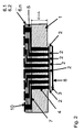
Bei dem in
Dabei sind auf einer Oberfläche des Substrates 1 wieder diskret und elektrisch isoliert zueinander Elektroden 2 ausgebildet. Auf den Elektroden 2 ist eine aktive Schicht 3 aus piezoelektrischem Werkstoff, die mit einer weiteren Elektrode 8 überdeckt ist, vorhanden.In this case,
Durch das Substrat 1 sind zu jeder einzelnen Elektrode 2 jeweils eine eigene Durchkontaktierung 4 bis zur Rückseite des Substrates 1 geführt. Auf dieser Rückseite sind bei diesem Beispiel sechs elektrisch nicht leitende Schichten 6.1 bis 6.6 als Mehrschichtaufbau ausgebildet. Auf den elektrisch isolierenden Schichten 6.1 bis 6.5 sind Leiterbahnen 7 ausgebildet, die mittels der Durchkontaktierungen 5 in den elektrisch nicht leitenden Schichten (6.1 bis 6.6) mit Kontaktflächen 10 elektrisch leitend verbunden sind. So wird erkennbar, dass bei einer kleinen für die Emittierung von Schallwellen nutzbaren Fläche, durch die Aufweitung eine viel größere Fläche für elektrische Anschlüsse an der Rückseite erhalten werden kann.Through the
Mit den
Beim in
Bei der in
Es können aber auch andere geometrische Elektrodenflächenformen als die hier gezeigten eingesetzt werden. Es besteht auch die Möglichkeit die Größe und/oder die Abstände von Elektroden 2 in einer Reihen- oder Matrixanordnung zu variieren.However, it is also possible to use other geometric electrode surface forms than those shown here. It is also possible the size and / or the distances of
Claims (12)
zwischen oder auf der/denen elektrische Leiterbahnen (7) vorhanden sind, die mittels weiterer Durchkontaktierungen (5), durch die elektrisch nicht leitende(n) Schicht(en) (6.1 bis 6.n) geführt sind, elektrisch leitend mit Kontaktflächen (10) auf der Rückseite des Substrates (1) verbunden sind und dabei die Kontaktflächen (10) auf einer Fläche verteilt sind, die größer als die Fläche der aktiven Schicht(en) (3) auf der Vorderseite des Substrates (1) ist.System according to claim 1, characterized in that at least one electrically non-conductive layer (6.1 to 6.6) is formed on the rear side of the substrate (1), which is opposite to the surface on which the electrodes (2) are formed,
between or on which / which electrical conductor tracks (7) are present, which are guided by means of further plated-through holes (5) through which the electrically nonconductive layer (s) (6.1 to 6.n) are electrically conductive with contact surfaces (10 ) are connected on the back side of the substrate (1) and the contact surfaces (10) are distributed on a surface which is larger than the area of the active layer (s) (3) on the front side of the substrate (1) is.
Priority Applications (1)
| Application Number | Priority Date | Filing Date | Title |
|---|---|---|---|
| EP09010474A EP2283935A1 (en) | 2009-08-13 | 2009-08-13 | Ultrasound converter system and method for its operation |
Applications Claiming Priority (1)
| Application Number | Priority Date | Filing Date | Title |
|---|---|---|---|
| EP09010474A EP2283935A1 (en) | 2009-08-13 | 2009-08-13 | Ultrasound converter system and method for its operation |
Publications (1)
| Publication Number | Publication Date |
|---|---|
| EP2283935A1 true EP2283935A1 (en) | 2011-02-16 |
Family
ID=41459788
Family Applications (1)
| Application Number | Title | Priority Date | Filing Date |
|---|---|---|---|
| EP09010474A Ceased EP2283935A1 (en) | 2009-08-13 | 2009-08-13 | Ultrasound converter system and method for its operation |
Country Status (1)
| Country | Link |
|---|---|
| EP (1) | EP2283935A1 (en) |
Cited By (2)
| Publication number | Priority date | Publication date | Assignee | Title |
|---|---|---|---|---|
| EP2631015A2 (en) | 2012-02-24 | 2013-08-28 | Fraunhofer-Gesellschaft zur Förderung der angewandten Forschung e.V. | Ultrasonic transducer for exciting and/or detecting ultrasound of various frequencies |
| DE102015210700A1 (en) * | 2015-06-11 | 2016-12-15 | Fraunhofer-Gesellschaft zur Förderung der angewandten Forschung e.V. | Method for detecting defects or defects in components using ultrasonic transducers |
Citations (7)
| Publication number | Priority date | Publication date | Assignee | Title |
|---|---|---|---|---|
| WO1996025244A1 (en) * | 1995-02-16 | 1996-08-22 | Precision Acoustics Limited | Electrical coupling for piezoelectric ultrasound detector |
| WO2003000337A2 (en) * | 2001-06-20 | 2003-01-03 | Bae Systems Information And Electronic Systems Integration Inc | Piezocomposite ultrasound array and integrated circuit assembly |
| US20030028108A1 (en) * | 2001-07-31 | 2003-02-06 | Miller David G. | System for attaching an acoustic element to an integrated circuit |
| JP2003079621A (en) * | 2001-09-14 | 2003-03-18 | Toshiba Corp | Ultrasonic probe and ultrasonic diagnostic device |
| US20030102777A1 (en) * | 2001-12-05 | 2003-06-05 | Fuji Photo Film Co., Ltd. | Ultrasonic transducer and method of manufacturing the same |
| US20030205947A1 (en) * | 2002-05-01 | 2003-11-06 | Klee Mareike Katharine | Ultrasonic membrane transducer for an ultrasonic diagnostic probe |
| JP2006122105A (en) * | 2004-10-26 | 2006-05-18 | Toshiba Corp | Ultrasonic probe |
-
2009
- 2009-08-13 EP EP09010474A patent/EP2283935A1/en not_active Ceased
Patent Citations (8)
| Publication number | Priority date | Publication date | Assignee | Title |
|---|---|---|---|---|
| WO1996025244A1 (en) * | 1995-02-16 | 1996-08-22 | Precision Acoustics Limited | Electrical coupling for piezoelectric ultrasound detector |
| WO2003000337A2 (en) * | 2001-06-20 | 2003-01-03 | Bae Systems Information And Electronic Systems Integration Inc | Piezocomposite ultrasound array and integrated circuit assembly |
| US20030013969A1 (en) * | 2001-06-20 | 2003-01-16 | Erikson Kenneth R. | Acoustical array with multilayer substrate integrated circuits |
| US20030028108A1 (en) * | 2001-07-31 | 2003-02-06 | Miller David G. | System for attaching an acoustic element to an integrated circuit |
| JP2003079621A (en) * | 2001-09-14 | 2003-03-18 | Toshiba Corp | Ultrasonic probe and ultrasonic diagnostic device |
| US20030102777A1 (en) * | 2001-12-05 | 2003-06-05 | Fuji Photo Film Co., Ltd. | Ultrasonic transducer and method of manufacturing the same |
| US20030205947A1 (en) * | 2002-05-01 | 2003-11-06 | Klee Mareike Katharine | Ultrasonic membrane transducer for an ultrasonic diagnostic probe |
| JP2006122105A (en) * | 2004-10-26 | 2006-05-18 | Toshiba Corp | Ultrasonic probe |
Non-Patent Citations (1)
| Title |
|---|
| YUAN YI-QUAN ET AL: "PVDF-DMOS SENSORS AND ARRAY FOR UNDERWATER ACOUSTIC IMAGING", ACOUSTICAL IMAGING. SENDAI, MAY 31 - JUNE 2, 1988; [PROCEEDINGS OF THE INTERNATIONAL SYMPOSIUM ACOUSTICAL IMAGING], vol. VOL. 17, 31 May 1988 (1988-05-31) - 2 June 1988 (1988-06-02), pages 609 - 617, XP000044002 * |
Cited By (6)
| Publication number | Priority date | Publication date | Assignee | Title |
|---|---|---|---|---|
| EP2631015A2 (en) | 2012-02-24 | 2013-08-28 | Fraunhofer-Gesellschaft zur Förderung der angewandten Forschung e.V. | Ultrasonic transducer for exciting and/or detecting ultrasound of various frequencies |
| DE102012003495A1 (en) | 2012-02-24 | 2013-08-29 | Fraunhofer-Gesellschaft zur Förderung der angewandten Forschung e.V. | Ultrasonic transducer for excitation and / or detection of ultrasound of different frequencies |
| DE102012003495B4 (en) * | 2012-02-24 | 2015-04-09 | Fraunhofer-Gesellschaft zur Förderung der angewandten Forschung e.V. | Ultrasonic transducer for excitation and / or detection of ultrasound of different frequencies |
| EP2631015A3 (en) * | 2012-02-24 | 2016-08-24 | Fraunhofer-Gesellschaft zur Förderung der angewandten Forschung e.V. | Ultrasonic transducer for exciting and/or detecting ultrasound of various frequencies |
| DE102015210700A1 (en) * | 2015-06-11 | 2016-12-15 | Fraunhofer-Gesellschaft zur Förderung der angewandten Forschung e.V. | Method for detecting defects or defects in components using ultrasonic transducers |
| DE102015210700B4 (en) | 2015-06-11 | 2023-11-09 | Fraunhofer-Gesellschaft zur Förderung der angewandten Forschung e.V. | Method for detecting errors or defects in components using ultrasonic transducers |
Similar Documents
| Publication | Publication Date | Title |
|---|---|---|
| DE102005053767B4 (en) | MEMS microphone, method of manufacture and method of installation | |
| US5655276A (en) | Method of manufacturing two-dimensional array ultrasonic transducers | |
| US5091893A (en) | Ultrasonic array with a high density of electrical connections | |
| US7148608B2 (en) | Multi-layer ceramic acoustic transducer | |
| JP4758634B2 (en) | Manufacturing method of multilayer ceramic acoustic transducer | |
| DE10151125A1 (en) | Connecting structure used in a testing arrangement for forming an electrical connection in semiconductor devices comprises a connecting substrate with through-holes, and connecting elements mounted on the horizontal surface of the substrate | |
| KR20060093469A (en) | Multilayered ultrasonic probe and fabricating method thereof | |
| TW201109668A (en) | Inspection socket | |
| US20060154075A1 (en) | Multilayered structure and method of manufacturing the same, and ultrasonic transducer | |
| DE102012003495B4 (en) | Ultrasonic transducer for excitation and / or detection of ultrasound of different frequencies | |
| EP2288912B1 (en) | Arrangement of a piezoacoustic resonator on an acoustic mirror of a substrate, method for the manufacture of the arrangement and use of the arrangement | |
| EP2313338A2 (en) | Process for manufacturing a component, process for manufacturing a component arrangement, component and component arrangement | |
| EP0166180B1 (en) | Hydrophone | |
| WO2008135004A1 (en) | Ultrasound converter array for applications in gaseous media | |
| EP2283935A1 (en) | Ultrasound converter system and method for its operation | |
| EP2817259B1 (en) | Method for producing a sensor | |
| DE102013110900B4 (en) | Probe for air-coupled ultrasound | |
| EP1989731B1 (en) | Method for manufacturing and making planar contact with an electronic apparatus | |
| JP2022552082A (en) | Acoustic transducer and manufacturing method | |
| DE102019218336B4 (en) | HIGH FREQUENCY ULTRASONIC TRANSDUCER AND METHOD OF MANUFACTURE | |
| Decharat et al. | High frequency copolymer ultrasonic transducer array of size-effective elements | |
| DE10018355A1 (en) | Ultrasound transducer; has piezoelectric body with several transducer elements and strip conductor foil on flat side with conductive track pattern to determine arrangement of transducer elements | |
| EP0040374A1 (en) | Ultrasonic transducer and method of manufacturing the same | |
| US10553779B2 (en) | Method of fabricating an acoustic transducer | |
| DE3019410A1 (en) | Ultrasound transducer for medical diagnostics or material testing - has numerous transducing elements and contacting simplified by using metal coated plastics foil for contacting |
Legal Events
| Date | Code | Title | Description |
|---|---|---|---|
| PUAI | Public reference made under article 153(3) epc to a published international application that has entered the european phase |
Free format text: ORIGINAL CODE: 0009012 |
|
| AK | Designated contracting states |
Kind code of ref document: A1 Designated state(s): AT BE BG CH CY CZ DE DK EE ES FI FR GB GR HR HU IE IS IT LI LT LU LV MC MK MT NL NO PL PT RO SE SI SK SM TR |
|
| AX | Request for extension of the european patent |
Extension state: AL BA RS |
|
| 17P | Request for examination filed |
Effective date: 20110815 |
|
| 17Q | First examination report despatched |
Effective date: 20141021 |
|
| STAA | Information on the status of an ep patent application or granted ep patent |
Free format text: STATUS: EXAMINATION IS IN PROGRESS |
|
| STAA | Information on the status of an ep patent application or granted ep patent |
Free format text: STATUS: THE APPLICATION HAS BEEN REFUSED |
|
| 18R | Application refused |
Effective date: 20200808 |