EP2283342B1 - Method for preparing a light-emitting device including quantum dots - Google Patents
Method for preparing a light-emitting device including quantum dots Download PDFInfo
- Publication number
- EP2283342B1 EP2283342B1 EP09727880.8A EP09727880A EP2283342B1 EP 2283342 B1 EP2283342 B1 EP 2283342B1 EP 09727880 A EP09727880 A EP 09727880A EP 2283342 B1 EP2283342 B1 EP 2283342B1
- Authority
- EP
- European Patent Office
- Prior art keywords
- layer
- transporting
- quantum dots
- accordance
- material capable
- Prior art date
- Legal status (The legal status is an assumption and is not a legal conclusion. Google has not performed a legal analysis and makes no representation as to the accuracy of the status listed.)
- Active
Links
Images








Classifications
-
- H—ELECTRICITY
- H10—SEMICONDUCTOR DEVICES; ELECTRIC SOLID-STATE DEVICES NOT OTHERWISE PROVIDED FOR
- H10K—ORGANIC ELECTRIC SOLID-STATE DEVICES
- H10K50/00—Organic light-emitting devices
- H10K50/10—OLEDs or polymer light-emitting diodes [PLED]
- H10K50/11—OLEDs or polymer light-emitting diodes [PLED] characterised by the electroluminescent [EL] layers
- H10K50/115—OLEDs or polymer light-emitting diodes [PLED] characterised by the electroluminescent [EL] layers comprising active inorganic nanostructures, e.g. luminescent quantum dots
-
- B—PERFORMING OPERATIONS; TRANSPORTING
- B82—NANOTECHNOLOGY
- B82Y—SPECIFIC USES OR APPLICATIONS OF NANOSTRUCTURES; MEASUREMENT OR ANALYSIS OF NANOSTRUCTURES; MANUFACTURE OR TREATMENT OF NANOSTRUCTURES
- B82Y20/00—Nanooptics, e.g. quantum optics or photonic crystals
-
- H—ELECTRICITY
- H05—ELECTRIC TECHNIQUES NOT OTHERWISE PROVIDED FOR
- H05B—ELECTRIC HEATING; ELECTRIC LIGHT SOURCES NOT OTHERWISE PROVIDED FOR; CIRCUIT ARRANGEMENTS FOR ELECTRIC LIGHT SOURCES, IN GENERAL
- H05B33/00—Electroluminescent light sources
- H05B33/12—Light sources with substantially two-dimensional [2D] radiating surfaces
- H05B33/14—Light sources with substantially two-dimensional [2D] radiating surfaces characterised by the chemical or physical composition or the arrangement of the electroluminescent material, or by the simultaneous addition of the electroluminescent material in or onto the light source
- H05B33/145—Arrangements of the electroluminescent material
-
- H—ELECTRICITY
- H10—SEMICONDUCTOR DEVICES; ELECTRIC SOLID-STATE DEVICES NOT OTHERWISE PROVIDED FOR
- H10K—ORGANIC ELECTRIC SOLID-STATE DEVICES
- H10K50/00—Organic light-emitting devices
- H10K50/10—OLEDs or polymer light-emitting diodes [PLED]
- H10K50/11—OLEDs or polymer light-emitting diodes [PLED] characterised by the electroluminescent [EL] layers
-
- H—ELECTRICITY
- H10—SEMICONDUCTOR DEVICES; ELECTRIC SOLID-STATE DEVICES NOT OTHERWISE PROVIDED FOR
- H10K—ORGANIC ELECTRIC SOLID-STATE DEVICES
- H10K50/00—Organic light-emitting devices
- H10K50/10—OLEDs or polymer light-emitting diodes [PLED]
- H10K50/14—Carrier transporting layers
-
- H—ELECTRICITY
- H10—SEMICONDUCTOR DEVICES; ELECTRIC SOLID-STATE DEVICES NOT OTHERWISE PROVIDED FOR
- H10K—ORGANIC ELECTRIC SOLID-STATE DEVICES
- H10K50/00—Organic light-emitting devices
- H10K50/10—OLEDs or polymer light-emitting diodes [PLED]
- H10K50/14—Carrier transporting layers
- H10K50/15—Hole transporting layers
- H10K50/155—Hole transporting layers comprising dopants
-
- H—ELECTRICITY
- H10—SEMICONDUCTOR DEVICES; ELECTRIC SOLID-STATE DEVICES NOT OTHERWISE PROVIDED FOR
- H10K—ORGANIC ELECTRIC SOLID-STATE DEVICES
- H10K50/00—Organic light-emitting devices
- H10K50/10—OLEDs or polymer light-emitting diodes [PLED]
- H10K50/17—Carrier injection layers
-
- H—ELECTRICITY
- H10—SEMICONDUCTOR DEVICES; ELECTRIC SOLID-STATE DEVICES NOT OTHERWISE PROVIDED FOR
- H10K—ORGANIC ELECTRIC SOLID-STATE DEVICES
- H10K50/00—Organic light-emitting devices
- H10K50/80—Constructional details
- H10K50/805—Electrodes
-
- H—ELECTRICITY
- H10—SEMICONDUCTOR DEVICES; ELECTRIC SOLID-STATE DEVICES NOT OTHERWISE PROVIDED FOR
- H10K—ORGANIC ELECTRIC SOLID-STATE DEVICES
- H10K59/00—Integrated devices, or assemblies of multiple devices, comprising at least one organic light-emitting element covered by group H10K50/00
- H10K59/10—OLED displays
- H10K59/12—Active-matrix OLED [AMOLED] displays
- H10K59/131—Interconnections, e.g. wiring lines or terminals
-
- H—ELECTRICITY
- H10—SEMICONDUCTOR DEVICES; ELECTRIC SOLID-STATE DEVICES NOT OTHERWISE PROVIDED FOR
- H10K—ORGANIC ELECTRIC SOLID-STATE DEVICES
- H10K59/00—Integrated devices, or assemblies of multiple devices, comprising at least one organic light-emitting element covered by group H10K50/00
- H10K59/80—Constructional details
- H10K59/82—Interconnections, e.g. terminals
-
- H—ELECTRICITY
- H10—SEMICONDUCTOR DEVICES; ELECTRIC SOLID-STATE DEVICES NOT OTHERWISE PROVIDED FOR
- H10K—ORGANIC ELECTRIC SOLID-STATE DEVICES
- H10K2101/00—Properties of the organic materials covered by group H10K85/00
- H10K2101/30—Highest occupied molecular orbital [HOMO], lowest unoccupied molecular orbital [LUMO] or Fermi energy values
Definitions
- the present invention relates to the technical field of devices including quantum dots.
- WO 2006/098540 A1 discloses a quantum dot light-emitting device which has an inorganic electron transport layer.
- the electron transport layer formed by an inorganic material is said to provide a high electron transport velocity or electron density, and to improve a light-emitting efficiency. Additionally, it is said that an interlayer resistance between an electrode and an organic electron transporting layer or between a quantum dot light-emitting layer and an organic electron transport layer is reduced, thus increasing a light emitting efficiency of the diode.
- a method for preparing a light-emitting device according to the present invention comprises the features defined in claim 1.
- Embodiments can comprise the features defined in the dependent claims.
- the material capable of transporting and injecting electrons is doped with a species to enhance electron transport characteristics of the inorganic material.
- a spacer layer can comprise an inorganic material.
- a spacer layer can comprise an organic material. Additional information concerning a spacer layer is provided below.
- a spacer layer comprises a material non-quenching to quantum dot emission.
- the hole injection material can comprise a material capable of transporting holes that is p-type doped.
- the device can have an initial turn-on voltage that is not greater than 1240/ ⁇ , wherein ⁇ represents the wavelength (nm) of light emitted by the emissive layer.
- light emission from the light emissive material occurs at a bias across the device that is less than the electron-Volt of the bandgap of the quantum dots in the emissive layer.
- quantum dots can include a core comprising a first material and a shell disposed over at least a portion of, and preferably substantially all, of the outer surface of the core, the shell comprising a second material.
- a quantum dot including a core and shell is also described herein as having a core/shell structure.
- more than one shell can be included in the core.
- the first material comprises an inorganic semiconductor material.
- the second material comprises an inorganic semiconductor material.
- quantum dots comprise inorganic semiconductor nanocrystals.
- inorganic semiconductor nanocrystals can comprise a core/shell structure.
- quantum dots comprise colloidally grown inorganic semiconductor nanocrystals.
- the quantum dots include a ligand attached to an outer surface thereof.
- two or more chemically distinct ligands can be attached to an outer surface of at least a portion of the quantum dots.
- an anode comprising a material with ⁇ 5eV work function can be used, thereby avoiding the need to utilize precious metals such as gold, etc.
- the electron and hole populations are balanced at the emissive layer of the device.
- the material capable of transporting holes comprises an organic material.
- an emissive layer can include two or more different types of quantum dots, wherein each type is selected to emit light having a predetermined wavelength.
- quantum dot types can be different based on, for example, factors such composition, structure and/or size of the quantum dot.
- quantum dots can be selected to emit at any predetermined wavelength across the electromagnetic spectrum.
- An emissive layer can include different types of quantum dots that have emissions at different wavelengths.
- the emissive layer includes quantum dots capable of emitting visible light.
- the emissive layer includes quantum dots capable of emitting infrared light.
- inorganic material and “organic material” may be further defined by a functional descriptor, depending on the desired function being addressed. In certain embodiments, the same material can address more than one function.
- horizontal zones are preferably parallel to the cathode.
- Figure 1 provides a schematic representation of an example of the architecture of a light-emitting device obtainable by a method according to one embodiment of the present invention.
- the light-emitting device 10 includes (from top to bottom) an anode 1, a layer comprising a hole injection material 2, a layer comprising a material capable of transporting holes (also referred to herein as a "hole transport material") 3, a layer including quantum dots 4, a layer comprising a material capable of transporting and injecting electrons (also referred to herein as an "electron transport material”) comprising an inorganic material 5, a cathode 6, and a substrate (not shown).
- the anode When voltage is applied across the anode and cathode, the anode injects holes into the hole injection material while the cathode injects electrons into the electron transport material.
- the injected holes and injected electrons combine to form an exciton on the quantum dot and emit light.
- the substrate (not shown) can be opaque or transparent.
- a transparent substrate can be used, for example, in the manufacture of a transparent light emitting device. See, for example, Bulovic, V. et al., Nature 1996, 380, 29 ; and Gu, G. et al., Appl. Phys. Lett. 1996, 68, 2606-2608 .
- the substrate can be rigid or flexible.
- the substrate can be plastic, metal, semiconductor wafer, or glass.
- the substrate can be a substrate commonly used in the art.
- the substrate has a smooth surface. A substrate surface free of defects is particularly desirable.
- the cathode 6 can be formed on the substrate (not shown).
- a cathode can comprise, ITO, aluminum, silver, gold, etc.
- the cathode preferably comprises a material with a work function chosen with regard to the quantum dots included in the device.
- the absolute value of the difference between E LUMO of the quantum dots and the work function of the cathode is less than about 0.5 eV.
- the absolute value of the difference between E LUMO of the quantum dots and the work function of the cathode is less than about 0.3 eV, and preferably less than about 0.2 eV.
- E LUMO of the quantum dots represents the energy level of the lowest unoccupied molecular orbital (LUMO) of the quantum dot.
- a cathode comprising indium tin oxide (ITO) can be preferred for use with an emissive material including quantum dots comprising a CdSe core/CdZnSe shell.
- Substrates including patterned ITO are commercially available and can be used in making a device according to the present invention.
- the layer comprising a material capable of transporting and injecting electrons 5 comprises an inorganic material comprising zinc oxide.
- Preferred inorganic semiconductor materials include those having a band gap that is greater than the emission energy of the emissive material.
- the absolute value of the difference between E LUMO of the quantum dots and E conduction band edge of material capable of transporting and injecting electrons is less than about 0.5 eV.
- the absolute value of the difference between E LUMO of the quantum dots and E conduction band edge of the material capable of transporting and injecting electrons is less than about 0.3 eV, and preferably less than about 0.2 eV
- E LUMO of the quantum dots represents the energy level of the lowest unoccupied molecular orbital (LUMO) of the quantum dots
- E of the conduction band edge of the material capable of transporting and injecting electrons represents the energy level of the conduction band edge of the material capable of transporting and injecting electrons.
- the inorganic semiconductor material can include a dopant.
- an electron transport material can include an n-type dopant.
- the inorganic semiconductor material for inclusion in an electron transport material of a device in accordance with the invention is zinc oxide.
- zinc oxide can be mixed or blended with one or more other inorganic materials, e.g., inorganic semiconductor materials, such as titanium oxide.
- the layer comprising a material capable of transporting and injecting electrons comprises zinc oxide.
- zinc oxide can be prepared, for example, by a sol-gel process.
- the zinc oxide can be chemically modified. Examples of chemical modification include treatment with hydrogen peroxide.
- a layer comprising a material capable of transporting and injecting electrons can comprise a mixture including zinc oxide and titanium oxide.
- the electron transport material is preferably included in the device as a layer.
- the layer has a thickness in a range from about 10 nm to 500 nm.
- Electron transport materials comprising an inorganic semiconductor material can be deposited at a low temperature, for example, by a known method, such as a vacuum vapor deposition method, an ion-plating method, sputtering, inkjet printing, sol-gel, etc.
- a vacuum vapor deposition method for example, an ion-plating method
- sputtering is typically performed by applying a high voltage across a low-pressure gas (for example, argon) to create a plasma of electrons and gas ions in a high-energy state.
- a low-pressure gas for example, argon
- Energized plasma ions strike a target of the desired coating material, causing atoms from that target to be ejected with enough energy to travel to, and bond with, the substrate.
- the layer comprising a material capable of transporting and injecting electrons can comprise a stratified structure comprising an inorganic material, wherein the stratified structure includes two or more horizontal zones having different conductivities.
- the layer can include a first zone at the upper portion of the layer (nearer the emissive layer) comprising an intrinsic or slightly n-type doped inorganic material (e.g., sputtered intrinsic or slightly n-type doped zinc oxide) with electron transporting characteristics, and a second zone at the lower portion of the layer (more remote from the emissive layer) comprising inorganic material that has a higher concentration of n-type doping than the material in the first zone (e.g., sputtered n-type doped ZnO) with electron injection characteristics.
- the layer can include three horizontal zones, e.g., a first zone at the upper portion of the layer (nearest the emissive layer) comprising an intrinsic inorganic material (e.g., sputtered intrinsic zinc oxide) which can be hole blocking; a second zone (between the first zone and the third zone) comprising an intrinsic or slightly n-type doped inorganic material (e.g., sputtered intrinsic or slightly n-type doped zinc oxide or another metal oxide) which can be electron transporting; and a third zone at the lowest portion of the layer (most remote from the emissive layer) comprising inorganic material that has a higher concentration of n-type doping than the material in the second zone (e.g., sputtered n-type doped ZnO or another metal oxide) which can be electron injecting.
- a first zone at the upper portion of the layer (nearest the emissive layer) comprising an intrinsic inorganic material e.g., sputtered intrinsic zinc oxide
- the inorganic material included in the stratified structure comprises zinc oxide.
- the inorganic material can comprise a mixture of two or more inorganic materials.
- Other inorganic materials can also be included in a stratified structure.
- the surface of the device on which an inorganic semiconductor material is to be formed can be cooled or heated for temperature control during the growth process.
- the temperature can affect the crystallinity of the deposited material as well as how it interacts with the surface it is being deposited upon.
- the deposited material can be polycrystalline or amorphous.
- the deposited material can have crystalline domains with a size in the range of 10 Angstroms to 1 micrometer.
- the doping concentration can be controlled by, for example, varying the gas, or mixture of gases, with a sputtering plasma technique. The nature and extent of doping can influence the conductivity of the deposited film, as well as its ability to optically quench neighboring excitons.
- the emissive material 4 includes quantum dots.
- the quantum dots comprise an inorganic semiconductor material.
- the quantum dots comprise crystalline inorganic semiconductor material (also referred to as semiconductor nanocrystals).
- preferred inorganic semiconductor materials include, but are not limited to, Group II- VI compound semiconductor nanocrystals, such as CdS, CdSe, ZnS, ZnSe, ZnTe, HgS, HgSe, HgTe, and other binary, ternary, and quaternary II-VI compositions; Group III-V compound semiconductor nanocrystals, such as GaP, GaAs, InP and InAs; PbS; PbSe; PbTe, and other binary, ternary, and quaternary III-V compositions.
- materials for the quantum dot light-emitting layer may be core-shell structured nanocrystals (for example, CdSe/ZnS, CdS/ZnSe, InP/ZnS, etc.) wherein the core is composed of a semiconductor nanocrystal (e.g. CdSe, CdS, etc.) and the shell is composed of a crystalline inorganic semiconductor material (e.g., ZnS, ZnSe, etc.).
- Quantum dots can also have various shapes, including, but not limited to, sphere, rod, disk, other shapes, and mixtures of various shaped particles.
- An emissive material can comprise one or more different quantum dots.
- the differences can be based, for example, on different composition, different size, different structure, or other distinguishing characteristic or property.
- the color of the light output of a light-emitting device can be controlled by the selection of the composition, structure, and size of the quantum dots included in a light-emitting device as the emissive material.
- the emissive material is preferably included in the device as a layer.
- the emissive layer can comprise one or more layers of the same or different emissive material(s).
- the emissive layer can have a thickness in a range from about 1 nm to about 20 nm.
- the emissive layer can have a thickness in a range from about 1 nm to about 10 nm.
- the emissive layer can have a thickness in a range from about 3 nm to about 6 about nm.
- the emissive layer can have a thickness of about 4 nm.
- a thickness of 4 nm can be preferred in a device including an electron transport material including a metal oxide.
- the quantum dots include one or more ligands attached to the surface thereof.
- a ligand can include an alkyl (e.g., C 1 -C 20 ) species.
- an alkyl species can be straight-chain, branched, or cyclic.
- an alkyl species can be substituted or unsubstituted.
- an alkyl species can include a hetero-atom in the chain or cyclic species.
- a ligand can include an aromatic species.
- an aromatic species can be substituted or unsubstituted.
- an aromatic species can include a hetero-atom. Additional information concerning ligands is provided herein and in various of the below-listed documents which are incorporated herein by reference.
- Quantum dots can be prepared by known techniques. Preferably they are prepared by a wet chemistry technique wherein a precursor material is added to a coordinating or non-coordinating solvent (typically organic) and nanocrystals are grown so as to have an intended size.
- a coordinating solvent typically organic
- the organic solvent is naturally coordinated to the surface of the quantum dots, acting as a dispersant. Accordingly, the organic solvent allows the quantum dots to grow to the nanometer-scale level.
- the wet chemistry technique has an advantage in that quantum dots of a variety of sizes can be uniformly prepared by appropriately controlling the concentration of precursors used, the kind of organic solvents, and preparation temperature and time, etc.
- the emission from a quantum dot capable of emitting light can be a narrow Gaussian emission band that can be tuned through the complete wavelength range of the ultraviolet, visible, or infra-red regions of the spectrum by varying the size of the quantum dot, the composition of the quantum dot, or both.
- a semiconductor nanocrystal comprising CdSe can be tuned in the visible region;
- a semiconductor nanocrystal comprising InAs can be tuned in the infra-red region.
- the narrow size distribution of a population of quantum dots capable of emitting light can result in emission of light in a narrow spectral range.
- the population can be monodisperse preferably exhibits less than a 15% rms (root-mean-square) deviation in diameter of such quantum dots, more preferably less than 10%, most preferably less than 5%.
- Spectral emissions in a narrow range of no greater than about 75 nm, no greater than about 60 nm, no greater than about 40 nm, and no greater than about 30 nm full width at half max (FWHM) for such quantum dots that emit in the visible can be observed.
- IR-emitting quantum dots can have a FWHM of no greater than 150 nm, or no greater than 100 nm.
- the emission can have a FWHM of no greater than 0.05 eV, or no greater than 0.03 eV.
- the breadth of the emission decreases as the dispersity of the light-emitting quantum dot diameters decreases.
- semiconductor nanocrystals can have high emission quantum efficiencies such as greater than 10%, 20%, 30%, 40%, 50%, 60%, 70%, 80%, or 90%.
- the narrow FWHM of semiconductor nanocrystals can result in saturated color emission.
- the broadly tunable, saturated color emission over the entire visible spectrum of a single material system is unmatched by any class of organic chromophores (see, for example, Dabbousi et al, J. Phys. Chem. 101, 9463 (1997 )).
- a monodisperse population of semiconductor nanocrystals will emit light spanning a narrow range of wavelengths.
- a pattern including more than one size of semiconductor nanocrystal can emit light in more than one narrow range of wavelengths.
- the color of emitted light perceived by a viewer can be controlled by selecting appropriate combinations of semiconductor nanocrystal sizes and materials.
- the degeneracy of the band edge energy levels of semiconductor nanocrystals facilitates capture and radiative recombination of all possible excitons.
- TEM Transmission electron microscopy
- Powder X-ray diffraction (XRD) patterns can provide the most complete information regarding the type and quality of the crystal structure of the semiconductor nanocrystals.
- Estimates of size are also possible since particle diameter is inversely related, via the X-ray coherence length, to the peak width.
- the diameter of the semiconductor nanocrystal can be measured directly by transmission electron microscopy or estimated from X-ray diffraction data using, for example, the Scherrer equation. It also can be estimated from the UV/Vis absorption spectrum.
- An emissive material can be deposited by spin-casting, screen-printing, inkjet printing, gravure printing, roll coating, drop-casting, Langmuir-Blodgett techniques, contact printing or other techniques known or readily identified by one skilled in the relevant art.
- a layer comprising a spacer material can be included between the emissive material and a layer of the device adjacent thereto, for example, an electron transport layer and/or a hole transport layer.
- a layer comprising a spacer material can promote better electrical interface between the emissive layer and the adjacent charge transport layer.
- a spacer material may comprise an organic material or an inorganic material.
- a spacer material comprises parylene.
- the spacer material comprises an ambipolar material. More preferably, it is non-quenching.
- a spacer material between the emissive layer and a hole transport layer can comprise an ambipolar host or hole transport material, or nanoparticles such as nickel oxide, and other metal oxides.
- Hole transport materials 3 include organic materials.
- An example of an organic material that can be included in a hole transport layer includes an organic chromophore.
- the organic chromophore can include a phenyl amine, such as, for example, N,N'-diphenyl-N,N'-bis(3-methylphenyl)-(1,1'-biphenyl)-4,4'-diamine (TPD).
- hole transport layer can include (N,N'-bis(3-methylphenyl)-N,N'-bis(phenyl)-spiro (spiro-TPD), 4-4'-N,N'-dicarbazolyl-biphenyl (CBP), 4,4-.bis[N-(1-naphthyl)-N-phenylamino]biphenyl (NPD), etc., a polyaniline, a polypyrrole, a poly(phenylene vinylene), copper phthalocyanine, an aromatic tertiary amine or polynuclear aromatic tertiary amine, a 4,4'-bis(p-carbazolyl)-1,1'-biphenyl compound, N,N,N',N'-tetraarylbenzidine, poly(3,4-ethylenedioxythiophene) (PEDOT)/polystyrene para-sulfonate (PSS) derivatives, poly-N-vin
- a hole transport layer comprises an organic small molecule material, a polymer, a spiro- compound (e.g., spiro-NPB), etc.
- Organic hole transport materials may be deposited by known methods such as a vacuum vapor deposition method, a sputtering method, a dip-coating method, a spin-coating method, a casting method, a bar-coating method, a roll-coating method, and other film deposition methods.
- organic layers are deposited under ultra-high vacuum (e.g., ⁇ 10'8 torr), high vacuum (e.g., from about 10'8 torr to about 10"5 torr), or low vacuum conditions (e.g., from about 10"5 torr to about 103 torr).
- the hole transport material is preferably included in the device as a layer.
- the layer can have a thickness in a range from about 10 nm to about 500 nm.
- the hole-injection material may comprise a separate hole injection material or may comprise an upper portion of the hole transport layer that has been doped, preferably p-type doped.
- the hole-injection material can be inorganic or organic. Examples of organic hole injection materials include, but are not limited to, LG-101 (see, for example, paragraph [0024] of EP 1 843 411 A1 ) and other HIL materials available from LG Chem, LTD. Other organic hole injection materials can be used. Examples of p-type dopants include, but are not limited to, stable, acceptor-type organic molecular material, which can lead to an increased hole conductivity in the doped layer, in comparison with a non-doped layer.
- a dopant comprising an organic molecular material can have a high molecular mass, such as, for example, at least 300 amu.
- dopants include, without limitation, F4-TCNQ, FeCl3, etc.
- doped organic materials for use as a hole injection material include, but are not limited to, an evaporated hole transport material comprising, e.g., 4, 4', 4"-tris (diphenylamino)triphenylamine (TDATA) that is doped with tetrafluoro-tetracyanoquinodimethane (F4-TCNQ); p-doped phthalocyanine (e.g., zinc-phthalocyanine (ZnPc) doped with F4-TCNQ (at, for instance, a molar doping ratio of approximately 1 :30); N,N'-diphenyl-N,N'-bis(1-naphthyl)-1,1 'biphenyl-4,
- anode 1 may comprise an electrically conductive metal or its oxide that can easily inject holes. Examples include, but are not limited to, ITO, aluminum, aluminum-doped zinc oxide (AZO), silver, gold, etc. Other suitable anode materials are known and can be readily ascertained by the skilled artisan.
- the anode material can be deposited using any suitable technique. In certain embodiments, the anode can be patterned.
- the light-emitting device may be fabricated by sequentially forming the cathode 6, the electron transport material comprising an inorganic material 5, the emissive material 4, the hole transport material 3, and the anode 2. This sequential approach avoids the deposition of the emissive material comprising quantum dots directly onto an organic material.
- an adhesion promoter can be included between the electron transport material and the emissive material.
- a suitable adhesion promoter is ozone treatment of the upper surface of the electron transport material.
- Other adhesion promoters can be used.
- the electrode (e.g., anode or cathode) materials and other materials are selected based on the light transparency characteristics thereof so that a device can be prepared that emits light from the top surface thereof.
- a top emitting device can be advantageous for constructing an active matrix device (e.g., a display).
- the electrode (e.g., anode or cathode) materials and other materials are selected based on light transparency characteristics thereof so that a device can be prepared that emits light from the bottom surface thereof.
- the device can further include a substrate (not shown in the figure).
- substrate materials include, without limitation, glass, plastic, insulated metal foil.
- a device can further include a passivation or other protective layer that can be used to protect the device from the environment.
- a protective glass layer can be included to encapsulate the device.
- a desiccant or other moisture absorptive material can be included in the device before it is sealed, e.g., with an epoxy, such as a UV curable epoxy. Other desiccants or moisture absorptive materials can be used.
- a method for preparing a light emitting device such as, for example, a device as illustrated in Figure 1 .
- the method comprising: forming a layer comprising a material capable of transporting and injecting electrons on a cathode, wherein the material capable of transporting and injecting electrons comprises an inorganic material; applying an emissive layer comprising quantum dots thereover; forming a layer comprising a material capable of transporting holes comprising an organic material over the emissive layer; forming a layer comprising a hole injection material over the layer comprising a material capable of transporting holes; and forming an anode over the layer comprising a hole injection material.
- Examples of materials that can be included in the method include those described herein.
- a light emitting device including a pair of electrodes, a layer comprising a light emissive material comprising quantum dots provided between the electrodes, and a layer comprising a material capable of transporting electrons comprising an inorganic material provided between the emissive layer and one of the electrodes, wherein the layer comprising the material capable of transporting electrons comprising an inorganic material comprises a stratified structure including two or more horizontal zones having different conductivities is formed.
- the inorganic material included in different zones of the stratified structure can be doped or undoped forms of the same or different materials.
- the inorganic material comprises an inorganic semiconductor material comprising zinc oxide.
- a first zone comprises an intrinsic inorganic semiconductor material
- a second zone adjacent thereto, can comprise a doped inorganic semiconductor material.
- the inorganic semiconductor material that is doped can be a doped form of the intrinsic material included in another zone of the stratified structure. While these examples describe a stratified structure including two zones, a stratified structure can include more than two zones.
- the inorganic semiconductor material included in different zones of the stratified structure can be doped or undoped forms of the same or different materials.
- the layer comprising a stratified structure can serve as a layer capable of transporting and injecting electrons.
- a zone in a layer comprising a stratified structure can have a predetermined conductivity so as to serve as a layer capable of transporting electrons, a layer capable of injecting electrons, and/or a layer capable of blocking holes.
- a zone can comprise a distinct layer.
- Examples of materials useful for the anode and cathode include those described elsewhere herein.
- Quantum dots included in the emissive layer can include those described elsewhere herein.
- different conductivities can be accomplished, for example, by changing the carrier mobility and/or charge density of the material.
- conduction properties of layers comprising a metal oxide are highly dependent on the concentration of oxygen in the layer structure since vacancies are the main mode of carrier conduction.
- two properties of the deposition can be altered.
- the power of deposition can be varied, increasing and decreasing the amount of oxygen that is incorporated in the layer.
- the powers and resulting conductivities are highly dependent on the material and the sputter system used. More oxygen can also be incorporated into the layer by adding oxygen to the sputter chamber gas environment which is often dominated by noble gases like Argon.
- Both the power and oxygen partial pressure can be used or customized to produce the desired layered metal oxide structure.
- Lowering the RF power during deposition can increase the conductivity of the layer, reducing the parasitic resistance of the layer.
- oxygen is incorporated into the deposition ambient to place a thin insulating surface on the layer formed.
- a light emitting device comprising a pair of electrodes and a layer of a light emissive material provided between the electrodes, wherein light emission from the light emissive material occurs at a bias voltage across the device that is less than the energy in electron-Volts of the bandgap of the emissive material is formed.
- the light emitting device includes an emissive material comprising quantum dots.
- quantum dots included in the emissive layer can include those described elsewhere herein.
- other well known light emissive materials can be used or included in the device.
- Examples of materials useful for the electrodes include those described elsewhere herein.
- additional layers described herein can also be included.
- the device comprises one of the light emitting devices taught herein.
- a light emitting device wherein the device has an initial turn-on voltage that is not greater than 1240/ ⁇ , wherein ⁇ represents the wavelength (nm) of light emitted by the emissive layer is formed.
- a light emitting device comprising a cathode, a layer comprising a material capable of transporting and injecting electrons comprising an inorganic material, an emissive layer comprising quantum dots, a layer comprising a material capable of transporting holes, a hole injection material, and an anode, the device having an initial turn-on voltage that is not greater than 1240/ ⁇ , wherein ⁇ represents the wavelength (nm) of light emitted by the emissive layer is formed.
- Examples of materials useful for the anode and cathode include those described elsewhere herein.
- Examples of materials useful for the layer comprising a material capable of transporting and injection electrons include those described elsewhere herein.
- Examples of materials useful for the layer comprising a material capable of transporting holes include those described elsewhere herein.
- Examples of materials useful for the layer comprising a hole injection material include those described elsewhere herein.
- additional layers described herein can also be included.
- the device comprises one of the light emitting devices taught herein.
- an additional hole transport material with a hole conductivity between that of the hole injection material and the hole transport material can be interposed between them.
- Additional hole transport materials can be interposed between two other hole conductive materials included in the device.
- any additional interposed hole transport material will have a hole conductivity that falls in-between those of the hole transport materials between which it is interposed.
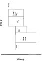
- Figure 2 schematically provides the band structure of an example of an embodiment of a light emitting device obtainable by a method according to the present invention.
- a metal oxide is used as a layer that is electron transporting and injecting and hole blocking. Such layer can be fabricated with solution process or thermal evaporation.
- the electron transport layer includes ZnO.
- ZnO can be preferably doped to form an ohmic contact with the cathode.
- the hole transport layer can comprise an organic material (e.g., small organic molecules (for example, TPD, spiro-TPB, NPB, spiro-NPB, etc.).
- the HTL can comprise an inorganic material.
- a hole injection layer (or p-type doped HTL) is also included in the depicted example to enhance hole supply from the anode.
- electrons are transported through the metal oxide and holes are transported through the HTL, excitons are generated in the quantum dot (QD) layer.
- QD quantum dot
- the composition and size of the quantum dots are selected to achieve light emission with a predetermined color or wavelength.
- a light-emitting device obtainable by a method according to the invention can be used to make a light-emitting device including red-emitting, green-emitting, and/or blue-emitting quantum dots.
- Other color light-emitting quantum dots can be included, alone or in combination with one or more other different quantum dots.
- separate layers of one or more different quantum dots may be desirable.
- a layer can include a mixture of two or more different quantum dots.
- the quantum dots included in the emissive layer may comprise red-emitting core/shell semiconductor nanocrystals (also abbreviated herein as "SOP”, “R-SOP”), green-emitting core/shell semiconductor nanocrystals (also abbreviated herein as “GQD”), blue-emitting core/shell semiconductor nanocrystals (also abbreviated herein as “BQD”), or yellow-emitting core/shell semiconductor nanocrystals (also abbreviated herein as "YQD”), which are prepared generally according to the following respective procedures. In any instances where a quantum dot is described by a "10X” modifier, the preparation is generally carried out on a scale approximately ten times that of the respective preparation procedure described below.
- SOP red-emitting core/shell semiconductor nanocrystals
- R-SOP red-emitting core/shell semiconductor nanocrystals
- GQD green-emitting core/shell semiconductor nanocrystals
- BQD blue-e
- Tri-n-octylphosphine oxide TOPO
- ODPA octadecylphosphonic acid
- Polycarbon 6.00 grams of Tri-n-octylphosphine oxide (TOPO) (99% Strem) and 0.668 grams of octadecylphosphonic acid (ODPA) (Polycarbon) are added to a 50 mL three necked round bottom flask. The ingredients are stirred and heated to a temperature of about 120°C. Once the flask reaches 120°C, the solution is degassed for 2 hours while maintained at 120°C. When the solution in the round bottom flask has finished degassing, the vacuum valve is closed and the flask is opened to nitrogen and stirred.
- TOPO Tri-n-octylphosphine oxide
- ODPA octadecylphosphonic acid
- Periodic samples are taken until an absorbance of ⁇ 560 nm is obtained, at which time the heating mantle is removed and the solution is permitted to cool while stirring.
- the temperature is 100 °C
- the solution is divided into half into 2 centrifuge tubes, and 2X volume of 3:1 methanol/isopropanol is added to each tube to precipitate semiconductor nanocrystal cores.
- the supernatant is poured off, and the semiconductor nanocrystal cores are mixed with hexane(minimum volume 2.5 mL in each tube).
- the contents of the two centrifuge tubes are then combined, centrifuged for 5 minutes at 4000 rpm, and filtered with hexane using a 0.2 micron filter.
- TOP Tri-n-octylphosphine
- the second syringe 4 mL of Tri-n-octylphosphine (TOP) (97% Strem) and 241.68 mg of Bis(TMS)sulfide.
- TOP Tri-n-octylphosphine
- the overcoating precursor mixture for each syringe is prepared by placing the Tri-n-octylphosphine into an 8 mL glass vial.
- the precursors dimethylcadmium, diethylzinc, or Bis(TMS)sulfide
- the solution is mixed gently with the vial capped and then drawn up into the 5 mL syringe.
- Micro capillary tubing is then loaded onto each syringe and a small amount of solution is pushed through to clear the tubing of nitrogen. (This can optionally be carried out inside a glove box).
- the vacuum is closed and the flask is opened up to nitrogen.
- the temperature of the flask is set to 70°C.
- the CdSe cores prepared (approximately 0.09 - to 0.1 mmol) as described above in hexane is added to the round bottom flask using a 5 mL syringe.
- the vacuum is slowly opened up and all of the hexane is removed from the flask, leaving behind the CdSe cores (this can take as long as an hour).
- the vacuum is closed and the flask is opened up to nitrogen.
- the syringe pump lines are removed from the flask.
- the temperature can be turned down to 100°C, and 10 mL of toluene can be added and allowed to sit overnight under nitrogen.
- the total growth solution is divided into two aliquots, each being put into a 50 mL centrifuge tube. An excess ⁇ 30 mL of a 3:1 MeOH/Isopropanol mixture is added to each centrifuge tube and stirred. The centrifuge tubes are centrifuged 5 minutes at 4000 rpm. The particles in each tube are dispersed in about 10 mL of hexane with stirring using a vortexer. The centrifuge tubes are then centrifuged for 5 minutes at 4000 rpm. The supernatant includes the hexane and the overcoated cores. The supernatant from each tube is placed into another two centrifuge tubes.
- the solid is a salt that has formed and is waste.
- the hexane/overcoated core supernatant is filtered using a 0.2 ⁇ m syringe filter. An excess of 3:1 methanol/isopropanol is added to each tube to precipitate the overcoated cores.
- the tubes are centrifuged for 5 minutes at 4000 rpm. The supernatant is poured off. The purified overcoated cores are now at the bottom of the tube and the supernatant is waste.
- ZnSe semiconductor nanocrystals are prepared by rapidly injecting 86 mg (0.7 mmol) diethyl zinc (Strem) and 1 mL tri-n-octylphosphine selenide (TOP) (97% Strem) (1M) dispersed in 5 mL of tri-n-octylphosphine (TOP) (97% Strem), into a round bottom flask containing 7 grams of degassed oleylamine (distilled from 98% Sigma-Aldrich and degassed at 120 °C under nitrogen with stirring) at 310°C and then growing at 270°C for 30 minutes to one hour.
- TOP tri-n-octylphosphine selenide
- TOP tri-n-octylphosphine
- a solution of 1.1 mmol dimethylcadmium (Strem) and 1.2 mL TOPSe (1M) dispersed in 8 mL TOP (97% Strem) is then introduced dropwise (1 drop/ ⁇ seconds) via a syringe pump into the ZnSe semiconductor nanocrystal growth solution/TOPO/HPA mixture, which is at 150 °C.
- the solution is then stirred at 150 °C for 21 hours.
- the CdZnSe cores are isolated by precipitating them out of solution twice with a miscible nonsolvent.
- the CdZnS shell is grown by introducing dropwise a solution of dimethylcadmium (20% of total moles of cation for a shell of predetermined thickness) (Strem), diethylzinc (Strem), and hexamethyldisithiane (2 fold excess of amount for a shell of predetermined thickness) (Fluka) in 8 mL of TOP into a degassed solution of 10 grams of TOPO (99% Strem) and 0.4 grams (2.4 mmol) HPA (Polycarbon Industries), which contains the CdZnSe cores, at a temperature of 140 °C (the CdZnSe cores dispersed in hexane are added to the degasses TOPO/HPA solution and the hexane is pulled off at 70 °C under vacuum prior to addition of the shell precursors).
- 0.050 g CdO (99.98% Puratronic) and 0.066 g of ZnO (99.99% Sigma Aldrich) is weighed out into a 100 mL three necked flask.
- 4 mL oleic acid (90% tech grade from Aldrich) and 32 mL octadecene (ODE) (90% tech grade from Aldrich) are added to the flask.
- the flask is set clamped on a heating mantle.
- One of the necks of the flask is fitted with a condenser connected to a Schlenck line through a vacuum adaptor.
- a temperature probe connected to a digital temperature controller is fitted to one of the two remaining flask necks.
- the third neck of the flask is then fitted with a septum cap.
- the contents of the flask are degassed at 80°C for 20 minutes in vacuo (200 millitorr).
- the contents of the three necked flask is stirred at a low stir rate (e.g., a setting of 4) and heated to 290°C and held for 20 minutes at that temperature. Then temperature is raised to 310°C under nitrogen. When the temperature reaches 305°C, stir rate is increased (e.g., from a setting of 4 to a setting of 5) and the sample is allowed to heat to 310°C until all the oxides have dissolved to give a clear solution. The temperature controller is then set to 300°C. Once the temperature falls to 300°C, approximately 8 mL of S in ODE is rapidly injected after which stir rate is maintained (e.g., at a setting of 5).
- a low stir rate e.g., a setting of 4
- stir rate is increased (e.g., from a setting of 4 to a setting of 5) and the sample is allowed to heat to 310°C until all the oxides have dissolved to give a clear solution.
- the temperature controller is then set to 300
- the temperature of the solution is observed to fall to about 265-270°C and climb back to 300C in ⁇ 5 minutes. After 3 hours, heating is stopped by removing the heating mantle and the flask is allowed to cool to room temperature. The contents of the flask are transferred to a degassed vial under nitrogen, which is transferred to an inert atmosphere box for further purification. Precipitation of dots may be observed, keep overnight in inert box.
- the purification method is as follows: The solution is divided in half, each half being added to a separate centrifuge tubes and centrifuged for 5 min, 4000rpm. For each tube, the solvent is poured off and the solid retained in the tube.
- the temperature in the flask is reduced to 70°C.
- Vacuum lines are closed and the flask is opened to a positive nitrogen atmosphere line.
- 3.3 mL cores (0.092 mmol) dispersed in hexane is drawn into a syringe in the glove box and injected into the flask.
- the nitrogen line is closed and the flask is slowly opened to the vacuum lines to extract hexane from the flask.
- Degassing is continued under vacuum until all of the hexane is removed. Once the degassing is completed, the vacuum lines are closed and positive nitrogen atmosphere is introduced into the flask.
- the needles on the syringes containing the precursor reagents are removed and replaced with microcapillary tubes, the other end of which is in vials through syringe needle. Air bubbles are removed from the syringes and the syringes are set on a syringe pump ready for injection of the contents into the flask. The flow rate of the syringe pump is adjusted for a flow rate of 50 microliters per minute.
- the temperature of the flaks is raised to 170°C.
- the end of the microcapillary tube attached to the syringe containing hexamethyl disilthiane is introduced into the second septa of the flask using an 18 gauge needle and place in such a way that the type of the microcapillary tube is immersed into the contents of the flask.
- the injection of hexamethyl disilthiane is started.
- the tip of the microcapillary tube of the other syringe containing the diethyl zinc precursor reagent is introduced into the flask with an 18 gauge needle through the other septum of the flask.
- the temperature of the flask is allowed to drop to 90°C and the contents of the flask is transferred into a degassed vial using a 20 mL syringe.
- the vial containing the reaction mixture is then transferred into the glove box for isolation of the nanoparticles from the reaction mixture.
- the temperature was brought back to 270°C where 4.4 mL of 1.5 M TBP-Se was then rapidly injected.
- the heating mantle was immediately removed from the reaction flask and the temperature of the reaction was allowed to cool to room temperature.
- the first absorption peak of the nanocrystals reached 515 nm.
- the CdSe cores were precipitated out of the growth solution inside a nitrogen atmosphere glovebox by adding a 3:1 mixture of methanol and isopropanol.
- the isolated cores were then dispersed in hexane and used to make core-shell materials.
- Dimethyl cadmium, diethyl zinc, and hexamethyldisilathiane were used as the Cd, Zn, and S precursors, respectively.
- the Cd and Zn were mixed in equimolar ratios while the S was in two-fold excess relative to the Cd and Zn.
- the Cd/Zn (0.37 mmol of dimethylcadmium and diethylzinc) and S (1.46 mmol of hexamethyldisilathiane) samples were each dissolved in 4 mL of trioctylphosphine inside a nitrogen atmosphere glove box. Once the precursor solutions were prepared, the reaction flask was heated to 155°C under nitrogen.
- the precursor solutions were added dropwise over the course of 2 hours at 155°C using a syringe pump.
- the nanocrystals were transferred to a nitrogen atmosphere glovebox and precipitated out of the growth solution by adding a 3:1 mixture of methanol and isopropanol.
- the resulting precipitate was then dispersed in hexane and precipitated out of solution for a second time by adding a 3:1 mixture of methanol and isopropanol.
- the isolated core-shell nanocrystals were then dispersed in hexane and used to make light emitting devices including quantum dots as described below.
- a standard device was fabricated that includes R-SOP (CdSe/CdZnS core-shell semiconductor nanocrystals) and charge transport layers comprising organic materials.
- the device was made as follows: Glass (50 mm x 50 mm) with patterned indium tin oxide (ITO) electrode on one surface (obtained from Osram Malaysia) is cleaned in an oxygen plasma for about 6 minutes to remove contaminants and oxygenate the surface. The cleaning takes place on 100% oxygen at about 20 psi. The glass is placed on a water cooled plate to help control the increase in temperature during cleaning.
- ITO indium tin oxide
- a layer of hole injection material (PEDOT, obtained from H.C. Starck, GmbH) (HIL) is spun onto the surface of the glass including the patterned electrode at a speed of 4000 RPM, to a thickness of about 750 Angstroms. This step is carried out under ambient conditions (i.e., not in a glove box).
- the PEDOT coated glass is then heated on a 120°C hot plate in a chamber ( ⁇ 20 ppm water & ⁇ 10 ppm oxygen), in a HEPA filter environment (approx. Class 1), in a nitrogen atmosphere for > 20 minutes to dry the PEDOT.
- the PEDOT coated glass is then allowed to cool to room temperature.
- a layer of hole transport material (N,N'-bis(3-methylphenyl)-N,N'-bis(phenyl)-spiro (spiro-TPD) (OLED grade, gradient sublimation purified) from Luminescent Technologies, Taiwan) is then evaporated onto the PEDOT layer in a deposition chamber (an ⁇ MOD chamber, obtained from Angstrom Engineering, Ottowa, Canada) after the chamber is pumped down to 10 -6 torr or better.
- spiro-TPD is referred to as E105.
- the spiro-TPD coated glass is then returned to the nitrogen environment and stamp-printed with an ink including the SOP CdSe/CdZnS core-shell semiconductor nanocrystals in hexane.
- the device was returned to the deposition chamber and pumped back down to 10 -6 torr or better for evaporation of the next layer, which can be a hole blocking layer or an electron transport layer.
- a layer of electron transport material of Alq3 (OLED grade, gradient sublimation purified) from Luminescent Technologies, Taiwan) is deposited.
- Each of the vapor deposited layers are patterned with use of shadow masks. After deposition of the electron transport material layer, the mask is changed before deposition of the metal cathode.
- Glass (50 mm x 50 mm) with patterned indium tin oxide (ITO) electrode on one surface (obtained from Osram Malaysia) is cleaned in an oxygen plasma for about 6 minutes to remove contaminants and oxygenate the surface.
- the cleaning takes place on 100% oxygen at about 20 psi.
- the glass is placed on a water cooled plate to help control the increase in temperature during cleaning.
- An electron transport layer comprising zinc oxide is prepared as follows.
- a zinc acetate [Zn(ac)] solution (157 g/L) in 96% 2-methoxy ethanol and 4% ethanolamine is spun coated at 2000 rpm onto the ITO.
- the zinc acetate was obtained from Sigma Aldrich.
- the metal oxide coated glass is then transferred into nitrogen-filled glove box, which normally has oxygen and water levels below 1 ppm.
- a coating formulation including quantum dots in hexane is spun coated on ZnO surface at 3000 rpm for 1 minute.
- the quantum dot film thickness is optimized by using various optical density solutions. Through the device performance optimization, the thickness of quantum dot film is kept around 25 nm, and is confirmed by atomic force microscopy (AFM).
- the device is returned to the deposition chamber and pumped back down to 10 -6 torr or better for evaporation of the next layer.
- a 50 nm layer of hole transport material (N,N'-bis(3-methylphenyl)-N,N'-bis(phenyl)-spiro (spiro-TPD) (OLED grade, gradient sublimation purified) from Luminescent Technologies, Taiwan)) is then evaporated onto the emissive layer in a deposition chamber (an ⁇ MOD chamber, obtained from Angstrom Engineering, Ottowa, Canada) after the chamber is pumped down to 10 -6 torr or better.
- the hole transport material are typically (OLED grade, gradient sublimation purified) obtained from Luminescent Technologies, Taiwan)).
- a hole injection layer (5% F4-TCNQ and E-105) (20 nm) is formed over the hole transport layer by co-evaporation techniques similar to those described above for preparing the hole transport layer.
- FIGS. 3-6 Various performance data for the devices of Table 1 are graphically presented in FIGS. 3-6 .
- FIGS. 3 and 4 graphically present performance data for the Red Device described in Table 1.
- FIG. 5 graphically presents performance data for the Green Device (A) and Blue Device (B) of the Examples. Lifetime improvements that can be achieved in certain embodiments of the invention are illustrated in FIG 6 , which graphically present lifetime data for the Red Device and the Standard Device of the Examples.
- a device is preferably baked or heated after fabrication, but before encapsulation.
- baking e.g., at 80°C on a hot plate in a nitrogen atmosphere
- the devices identified in Table 2 were generally fabricated as set forth below. The details of each device (materials, thicknesses, etc) are set forth in Table 2 below. (Layer thicknesses for the test devices are listed in Table 2 parenthetically.)
- TiOx The sol-gel procedure for producing TiOx is as follows: titanium(IV) isopropoxide (Ti[OCH(CH 3 ) 2 ]4, Aldrich, 99.999 %, 10 mL) was prepared as a precursor and mixed with 2-methoxyethanol (CH 3 OCH 2 CH 2 OH, Aldrich, 99.9+ %, 50 mL) and ethanolamine (H 2 NCH 2 CH 2 OH, Aldrich, 99+ %, 5 mL) in a three-necked flask equipped with a condenser, a thermometer, and an argon-gas inlet/outlet.
- Ti[OCH(CH 3 ) 2 ]4, Aldrich, 99.999 %, 10 mL was prepared as a precursor and mixed with 2-methoxyethanol (CH 3 OCH 2 CH 2 OH, Aldrich, 99.9+ %, 50 mL) and ethanolamine (H 2 NCH 2 CH 2 OH, Aldrich, 99
- the typical TiOx precursor solution was prepared in isopropyl alcohol.
- Test devices identified in Table 2 that include a ZnO layer were fabricated on patterned ITO substrates that were sonicated in acetone and isopropyl alcohol for 10 minutes each, followed by 6 minutes O 2 plasma treatment.
- the spin coating sol-gel formulations used to fabricate a mixed ZnO-TiOx layer utilized a mixture of a ZnO spin coating sol-gel formulation (prepared substantially as described above) and a TiOx spin coating sol-gel formulation (prepared substantially as described above).
- the ZnO and TiOx formulations are mixed in a predetermined proportion.
- ITO indium tin oxide
- An electron transport layer comprising a metal oxide was formed by sol-gel technique (ZnO and/or TiO x , as indicated in Table 2). prepared substantially as described above).
- the metal oxide coated glass is then returned to the nitrogen environment and spin-coated with an ink including quantum dots in hexane.
- post-baking on partial finished device at 80°C on hot plate is favorable. Then, the device is returned to the deposition chamber and pumped back down to 10 -7 torr or better for evaporation of the next layer.
- a layer of hole transport material is then evaporated onto the emissive layer in a deposition chamber (an ⁇ MOD chamber, obtained from Angstrom Engineering, Ottowa, Canada) after the chamber is pumped down to 10 -7 torr or better.
- the hole transport material are typically (OLED grade, gradient sublimation purified) obtained from Luminescent Technologies, Taiwan).
- a hole injection layer is included in the device, it is formed over the hole transport layer.
- Each of the vapor deposited layers are patterned with use of shadow masks. After deposition of the hole transport material layer and hole injection layer, the mask is changed before deposition of the metal anode.
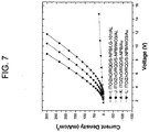
- FIG. 7 shows I-V curves of inverted structures with LG-101 and WO3 as hole injection layers respectively.
- Device K is inverted structure with no hole injection layer. From the data, device K has insufficient current injection through anode.
- FIG.8 shows device luminance efficiency in different device structures.
- the most efficient device is a device in accordance with an embodiment of the invention that includes small molecular material LG 101 as hole injection layer. Without a hole injection layer, luminance (see Device K) is not observable.
- FIG.9 shows the luminance efficiency of a device without an electron transport & injection layer and without a hole blocking layer.
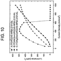
- FIG.10 shows luminance of inverted device without an electron transport & injection layer and without a hole blocking layer.
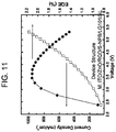
- FIG. 11 shows device performance for a device in accordance with an embodiment of the invention that includes an emissive layer including red-light emitting quantum dots.
- Peak external quantum efficiency (EQE) 2.1% reaches at 3.46 v with brightness of 9671 nits.
- FIG.12 shows a device in accordance with an embodiment of the invention that includes an emissive layer including red-light emitting quantum dots operating at very low voltage.
- Inset is EL spectrum of this device. It is noticed that the turn on voltage for this device is extremely low.
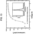
- FIG. 13 shows a device in accordance with an embodiment of the invention that includes an emissive layer including yellow-light emitting quantum dots operating at very low voltage.
- the turn on voltage for this device is below the energy required to overcome band gap of yellow emitter, which is 2.1 V.
- Inset is EL spectrum of a yellow quantum dot light emitting device. Peak brightness 41300 cd/m2 is obtained at 8V.
- FIG. 14 shows efficiency of Device N at certain luminance.
- the peak luminance efficiency 9.8 lm/W reaches at 3V with 2620 nits.
- the peak luminance efficiency 9.46 cd/A reaches at 3.5V with 6800 nits.
- FIG. 15 shows examples of mixing ZnO with TiOx, which may improve the device efficiency by charge balance.
- Light-emitting devices obtainable by methods in accordance with various embodiments of the invention may be incorporated into a wide variety of consumer products, including flat panel displays, computer monitors, televisions, billboards, lights for interior or exterior illumination and/or signaling, heads up displays, fully transparent displays, flexible displays, laser printers, telephones, cell phones, personal digital assistants (PDAs), laptop computers, digital cameras, camcorders, viewfinders, micro-displays, vehicles, a large area wall, theater or stadium screen, a sign, lamps and various solid state lighting devices.
- PDAs personal digital assistants
- laptop computers digital cameras, camcorders, viewfinders, micro-displays, vehicles, a large area wall, theater or stadium screen, a sign, lamps and various solid state lighting devices.
- PCT/US2007/00341 1 filed 02/08/2007, of Beatty, et al., for "Device Including Semiconductor Nanocrystals And A Layer Including A Doped Organic Material And Methods"; International Application No. PCT/US2007/1471 1 , filed 06/25/2007, of Coe-Sullivan, for "Methods For Depositing Nanomaterial, Methods For Fabricating A Device, And Methods For Fabricating An Array Of Devices"; International Application No.
- PCT/US2007/008721 filed 04/03/2007, of Cox, et al., for "Methods Of Depositing Nanomaterial & Methods Of Making A Device”
- International Application No. PCT/US2007/019797 filed 09/12/2007, of Coe-Sullivan, et al., for "A Composite Including Nanoparticles, Methods, And Products Including A Composite”
- International Application No. PCT/US2007/019796 of Coe-Sullivan, et al., filed 09/12/2007, for "Electroluminescent Display Useful For Displaying A Predetermined Pattern”; International Application No.
- PCT/US2007/24305 filed 1 1/21/2007, of Breen, et al., for "Blue Light Emitting Semiconductor Nanocrystal And Compositions And Devices Including Same”
- International Application No. PCT/US2007/24306 filed 1 1/21/2007, of Ramprasad, for "Semiconductor Nanocrystal And Compositions And Devices Including Same”
- International Application No. PCT/US2007/013152 filed 06/04/2007, of Coe-Sullivan, et al., for "Light-Emitting Devices And Displays With Improved Performance”; International Application No.
- PCT/US2007/24750 of Coe-Sullivan, et al., filed 12/03/2007 "Improved Composites And Devices Including Nanoparticles"; International Application No. PCT/US2007/24310 , filed 1 1/21/2007, of Kazlas, et al., for "Light-Emitting Devices And Displays With Improved Performance”; International Application No. PCT/US2007/003677 , filed 02/14/2007, of Bulovic, et al., for "Solid State Lighting Devices Including Semiconductor Nanocrystals & Methods", U.S. Patent Application No.
- top and bottom are relative positional terms, based upon a location from a reference point. More particularly, “top” means furthest away from the substrate, while “bottom” means closest to the substrate.
- the bottom electrode is the electrode closest to the substrate, and is generally the first electrode fabricated; the top electrode is the electrode that is more remote from the substrate, on the top side of the light-emitting material.
- the bottom electrode has two surfaces, a bottom surface closest to the substrate, and a top surface further away from the substrate.
- a first layer is described as disposed or deposited “over” a second layer
- the first layer is disposed further away from substrate.
- There may be other layers between the first and second layer unless it is otherwise specified.
- a cathode may be described as "disposed over" an anode, even though there are various organic and/or inorganic layers in between.
Landscapes
- Physics & Mathematics (AREA)
- Optics & Photonics (AREA)
- Engineering & Computer Science (AREA)
- Chemical & Material Sciences (AREA)
- Nanotechnology (AREA)
- Crystallography & Structural Chemistry (AREA)
- Life Sciences & Earth Sciences (AREA)
- Biophysics (AREA)
- Inorganic Chemistry (AREA)
- Microelectronics & Electronic Packaging (AREA)
- Electroluminescent Light Sources (AREA)
- Luminescent Compositions (AREA)
Description
- The present invention relates to the technical field of devices including quantum dots.
-
WO 2006/098540 A1 discloses a quantum dot light-emitting device which has an inorganic electron transport layer. The electron transport layer formed by an inorganic material is said to provide a high electron transport velocity or electron density, and to improve a light-emitting efficiency. Additionally, it is said that an interlayer resistance between an electrode and an organic electron transporting layer or between a quantum dot light-emitting layer and an organic electron transport layer is reduced, thus increasing a light emitting efficiency of the diode. - A method for preparing a light-emitting device according to the present invention comprises the features defined in
claim 1. - Embodiments can comprise the features defined in the dependent claims.
- In certain embodiments, the material capable of transporting and injecting electrons is doped with a species to enhance electron transport characteristics of the inorganic material.
- A spacer layer can comprise an inorganic material. A spacer layer can comprise an organic material. Additional information concerning a spacer layer is provided below.
- In certain preferred embodiments, a spacer layer comprises a material non-quenching to quantum dot emission.
- In certain embodiments, the hole injection material can comprise a material capable of transporting holes that is p-type doped.
- In certain embodiments, the device can have an initial turn-on voltage that is not greater than 1240/λ, wherein λ represents the wavelength (nm) of light emitted by the emissive layer.
- In certain embodiments, light emission from the light emissive material occurs at a bias across the device that is less than the electron-Volt of the bandgap of the quantum dots in the emissive layer.
- In certain embodiments, quantum dots can include a core comprising a first material and a shell disposed over at least a portion of, and preferably substantially all, of the outer surface of the core, the shell comprising a second material. (A quantum dot including a core and shell is also described herein as having a core/shell structure.) In certain embodiments, more than one shell can be included in the core. In certain embodiments, the first material comprises an inorganic semiconductor material. In certain embodiments, the second material comprises an inorganic semiconductor material.
- In certain embodiments, quantum dots comprise inorganic semiconductor nanocrystals. In certain embodiments, inorganic semiconductor nanocrystals can comprise a core/shell structure. In certain preferred embodiments, quantum dots comprise colloidally grown inorganic semiconductor nanocrystals.
- In certain embodiments, at least a portion of the quantum dots include a ligand attached to an outer surface thereof. In certain embodiments, two or more chemically distinct ligands can be attached to an outer surface of at least a portion of the quantum dots. In certain embodiments, an anode comprising a material with < 5eV work function can be used, thereby avoiding the need to utilize precious metals such as gold, etc.
- In certain embodiments, the electron and hole populations are balanced at the emissive layer of the device. The material capable of transporting holes comprises an organic material.
- In certain embodiments of the present invention taught are taught herein, an emissive layer can include two or more different types of quantum dots, wherein each type is selected to emit light having a predetermined wavelength. In certain embodiments, quantum dot types can be different based on, for example, factors such composition, structure and/or size of the quantum dot. In certain embodiments, quantum dots can be selected to emit at any predetermined wavelength across the electromagnetic spectrum. An emissive layer can include different types of quantum dots that have emissions at different wavelengths.
- In certain embodiments, the emissive layer includes quantum dots capable of emitting visible light.
- In certain embodiments, the emissive layer includes quantum dots capable of emitting infrared light.
- As used herein, the terms "inorganic material" and "organic material" may be further defined by a functional descriptor, depending on the desired function being addressed. In certain embodiments, the same material can address more than one function.
- In some embodiments, it may be desirable to have different conductivities which can be accomplished, for example, by changing the carrier mobility and/or charge density of a material in a zone and/or layer.
- In certain embodiments including a stratified structure, horizontal zones are preferably parallel to the cathode.
- Other aspects and embodiments of the invention relate to materials and methods that are useful in making the above described light-emitting devices, displays, and other products including the above-described light-emitting device.
- The foregoing, and other aspects described herein, all constitute embodiments of the present invention.
- It is to be understood that both the foregoing general description and the following detailed description are exemplary and explanatory only and are not restrictive of the invention as claimed. Other embodiments will be apparent to those skilled in the art from consideration of the description and drawings, from the claims, and from practice of the invention disclosed herein.
- In the drawings:
-
FIG. 1 is schematic drawing depicting an example of an embodiment of a light-emitting device structure in accordance with the invention. -
FIG. 2 provides a schematic band structure of an example of an embodiment of a light-emitting device in accordance with the invention. -
FIGS. 3 &4 graphically present performance data for the Red Light Emitting Device of the Examples. -
FIG. 5 graphically presents performance data for the Green Light Emitting Device (A) and the Blue Light emitting Device (B) of the Examples. -
FIG. 6 graphically compares lifetime data for the Red Light Emitting Device of the Examples (indicated as "inverted structure" in the figure) and the Standard Light Emitting Device (a comparative device) described in the Examples (indicated as "standard structure" in the figure). -
FIG. 7 depicts an I (current)-V (voltage) curves for devices that include hole injection layers and a device without a hole injection layer. -
FIG. 8 shows device luminance efficiency for different device structures. -
FIG. 9 shows luminance efficiency of a device without an electron transport and hole blocking layer. -
FIG. 10 shows luminance of inverted device without either a hole blocking or electron transport and injection layer. -
FIG. 11 shows performance data for an example of device in accordance with an embodiment of the invention. -
FIG. 12 shows operating voltage for an example of a red light emitting device in accordance with an embodiment of the invention. -
FIG. 13 shows operating voltage for an example of an orange light emitting device in accordance with an embodiment of the invention. -
FIG. 14 shows efficiency at certain luminance for an example of an orange light emitting device in accordance with an embodiment of the invention. -
FIG. 15 shows performance for an example of a device in accordance with any embodiment of the invention. - The attached figures are simplified representations presented for purposes of illustration only; the actual structures may differ in numerous respects, including, e.g., relative scale, etc.
- For a better understanding to the present invention, together with other advantages and capabilities thereof, reference is made to the following disclosure and appended claims in connection with the above-described drawings.
-
Figure 1 provides a schematic representation of an example of the architecture of a light-emitting device obtainable by a method according to one embodiment of the present invention. Referring toFigure 1 , the light-emitting device 10 includes (from top to bottom) ananode 1, a layer comprising ahole injection material 2, a layer comprising a material capable of transporting holes (also referred to herein as a "hole transport material") 3, a layer includingquantum dots 4, a layer comprising a material capable of transporting and injecting electrons (also referred to herein as an "electron transport material") comprising aninorganic material 5, acathode 6, and a substrate (not shown). When voltage is applied across the anode and cathode, the anode injects holes into the hole injection material while the cathode injects electrons into the electron transport material. The injected holes and injected electrons combine to form an exciton on the quantum dot and emit light. - The substrate (not shown) can be opaque or transparent. A transparent substrate can be used, for example, in the manufacture of a transparent light emitting device. See, for example, Bulovic, V. et al., Nature 1996, 380, 29; and Gu, G. et al., Appl. Phys. Lett. 1996, 68, 2606-2608. The substrate can be rigid or flexible. The substrate can be plastic, metal, semiconductor wafer, or glass. The substrate can be a substrate commonly used in the art. Preferably the substrate has a smooth surface. A substrate surface free of defects is particularly desirable.
- The
cathode 6 can be formed on the substrate (not shown). In certain embodiments, a cathode can comprise, ITO, aluminum, silver, gold, etc. The cathode preferably comprises a material with a work function chosen with regard to the quantum dots included in the device. In certain embodiments, the absolute value of the difference between ELUMO of the quantum dots and the work function of the cathode is less than about 0.5 eV. In certain embodiments the absolute value of the difference between ELUMO of the quantum dots and the work function of the cathode is less than about 0.3 eV, and preferably less than about 0.2 eV. ELUMO of the quantum dots represents the energy level of the lowest unoccupied molecular orbital (LUMO) of the quantum dot. For example, a cathode comprising indium tin oxide (ITO) can be preferred for use with an emissive material including quantum dots comprising a CdSe core/CdZnSe shell. - Substrates including patterned ITO are commercially available and can be used in making a device according to the present invention.
- The layer comprising a material capable of transporting and injecting
electrons 5 comprises an inorganic material comprising zinc oxide. Preferred inorganic semiconductor materials include those having a band gap that is greater than the emission energy of the emissive material. In certain embodiments, the absolute value of the difference between ELUMO of the quantum dots and E conduction band edge of material capable of transporting and injecting electrons, is less than about 0.5 eV. In certain embodiments, the absolute value of the difference between ELUMO of the quantum dots and E conduction band edge of the material capable of transporting and injecting electrons, is less than about 0.3 eV, and preferably less than about 0.2 eV ELUMO of the quantum dots represents the energy level of the lowest unoccupied molecular orbital (LUMO) of the quantum dots; E of the conduction band edge of the material capable of transporting and injecting electrons represents the energy level of the conduction band edge of the material capable of transporting and injecting electrons. - In certain embodiments, the inorganic semiconductor material can include a dopant.
- In certain preferred embodiments, an electron transport material can include an n-type dopant.
- The inorganic semiconductor material for inclusion in an electron transport material of a device in accordance with the invention is zinc oxide. In certain embodiments, zinc oxide can be mixed or blended with one or more other inorganic materials, e.g., inorganic semiconductor materials, such as titanium oxide.
- As mentioned above, the layer comprising a material capable of transporting and injecting electrons comprises zinc oxide. Such zinc oxide can be prepared, for example, by a sol-gel process. In certain embodiments, the zinc oxide can be chemically modified. Examples of chemical modification include treatment with hydrogen peroxide.
- In other preferred embodiments, a layer comprising a material capable of transporting and injecting electrons can comprise a mixture including zinc oxide and titanium oxide.
- The electron transport material is preferably included in the device as a layer. In certain embodiments, the layer has a thickness in a range from about 10 nm to 500 nm.
- Electron transport materials comprising an inorganic semiconductor material can be deposited at a low temperature, for example, by a known method, such as a vacuum vapor deposition method, an ion-plating method, sputtering, inkjet printing, sol-gel, etc. For example, sputtering is typically performed by applying a high voltage across a low-pressure gas (for example, argon) to create a plasma of electrons and gas ions in a high-energy state. Energized plasma ions strike a target of the desired coating material, causing atoms from that target to be ejected with enough energy to travel to, and bond with, the substrate.
- In certain embodiments, the layer comprising a material capable of transporting and injecting electrons can comprise a stratified structure comprising an inorganic material, wherein the stratified structure includes two or more horizontal zones having different conductivities. For example, in certain embodiments, the layer can include a first zone at the upper portion of the layer (nearer the emissive layer) comprising an intrinsic or slightly n-type doped inorganic material (e.g., sputtered intrinsic or slightly n-type doped zinc oxide) with electron transporting characteristics, and a second zone at the lower portion of the layer (more remote from the emissive layer) comprising inorganic material that has a higher concentration of n-type doping than the material in the first zone (e.g., sputtered n-type doped ZnO) with electron injection characteristics.
- In another example, in certain embodiments, the layer can include three horizontal zones, e.g., a first zone at the upper portion of the layer (nearest the emissive layer) comprising an intrinsic inorganic material (e.g., sputtered intrinsic zinc oxide) which can be hole blocking; a second zone (between the first zone and the third zone) comprising an intrinsic or slightly n-type doped inorganic material (e.g., sputtered intrinsic or slightly n-type doped zinc oxide or another metal oxide) which can be electron transporting; and a third zone at the lowest portion of the layer (most remote from the emissive layer) comprising inorganic material that has a higher concentration of n-type doping than the material in the second zone (e.g., sputtered n-type doped ZnO or another metal oxide) which can be electron injecting.
- The inorganic material included in the stratified structure comprises zinc oxide. In certain embodiments, the inorganic material can comprise a mixture of two or more inorganic materials. Other inorganic materials can also be included in a stratified structure.
- Additional information concerning inorganic materials that may be useful for inclusion in an electron transport layer is disclosed in
International Application No. PCT/US2006/005184, filed 15 February 2006 , for "Light Emitting Device Including Semiconductor Nanocrystals, which published asWO 2006/088877 on 26 August 2006 . - The surface of the device on which an inorganic semiconductor material is to be formed can be cooled or heated for temperature control during the growth process. The temperature can affect the crystallinity of the deposited material as well as how it interacts with the surface it is being deposited upon. The deposited material can be polycrystalline or amorphous. The deposited material can have crystalline domains with a size in the range of 10 Angstroms to 1 micrometer. If doped, the doping concentration can be controlled by, for example, varying the gas, or mixture of gases, with a sputtering plasma technique. The nature and extent of doping can influence the conductivity of the deposited film, as well as its ability to optically quench neighboring excitons.
- The
emissive material 4 includes quantum dots. In certain embodiments, the quantum dots comprise an inorganic semiconductor material. In certain preferred embodiments, the quantum dots comprise crystalline inorganic semiconductor material (also referred to as semiconductor nanocrystals). Examples of preferred inorganic semiconductor materials include, but are not limited to, Group II- VI compound semiconductor nanocrystals, such as CdS, CdSe, ZnS, ZnSe, ZnTe, HgS, HgSe, HgTe, and other binary, ternary, and quaternary II-VI compositions; Group III-V compound semiconductor nanocrystals, such as GaP, GaAs, InP and InAs; PbS; PbSe; PbTe, and other binary, ternary, and quaternary III-V compositions. Other non-limiting examples of inorganic semiconductor materials include Group II-V compounds, Group III-VI compounds, , Group IV-VI compounds, Group I-III-VI compounds, Group II-IV-VI compounds, Group II-IV-V compounds, Group IV elements, an alloy including any of the foregoing, and/or a mixture including any of the foregoing. Further, materials for the quantum dot light-emitting layer may be core-shell structured nanocrystals (for example, CdSe/ZnS, CdS/ZnSe, InP/ZnS, etc.) wherein the core is composed of a semiconductor nanocrystal (e.g. CdSe, CdS, etc.) and the shell is composed of a crystalline inorganic semiconductor material (e.g., ZnS, ZnSe, etc.). - Quantum dots can also have various shapes, including, but not limited to, sphere, rod, disk, other shapes, and mixtures of various shaped particles.
- An emissive material can comprise one or more different quantum dots. The differences can be based, for example, on different composition, different size, different structure, or other distinguishing characteristic or property.
- The color of the light output of a light-emitting device can be controlled by the selection of the composition, structure, and size of the quantum dots included in a light-emitting device as the emissive material.
- The emissive material is preferably included in the device as a layer. In certain embodiments, the emissive layer can comprise one or more layers of the same or different emissive material(s). In certain embodiments, the emissive layer can have a thickness in a range from about 1 nm to about 20 nm. In certain embodiments, the emissive layer can have a thickness in a range from about 1 nm to about 10 nm. In certain embodiments, the emissive layer can have a thickness in a range from about 3 nm to about 6 about nm. In certain embodiments, the emissive layer can have a thickness of about 4 nm. A thickness of 4 nm can be preferred in a device including an electron transport material including a metal oxide.
- Preferably, the quantum dots include one or more ligands attached to the surface thereof. In certain embodiments, a ligand can include an alkyl (e.g., C1-C20) species. In certain embodiments, an alkyl species can be straight-chain, branched, or cyclic. In certain embodiments, an alkyl species can be substituted or unsubstituted. In certain embodiments, an alkyl species can include a hetero-atom in the chain or cyclic species. In certain embodiments, a ligand can include an aromatic species. In certain embodiments, an aromatic species can be substituted or unsubstituted. In certain embodiments, an aromatic species can include a hetero-atom. Additional information concerning ligands is provided herein and in various of the below-listed documents which are incorporated herein by reference.
- By controlling the structure, shape and size of quantum dots during preparation, energy levels over a very broad range of wavelengths can be obtained while the properties of the bulky materials are varied. Quantum dots (including but not limited to semiconductor nanocrystals) can be prepared by known techniques. Preferably they are prepared by a wet chemistry technique wherein a precursor material is added to a coordinating or non-coordinating solvent (typically organic) and nanocrystals are grown so as to have an intended size. According to the wet chemistry technique, when a coordinating solvent is used, as the quantum dots are grown, the organic solvent is naturally coordinated to the surface of the quantum dots, acting as a dispersant. Accordingly, the organic solvent allows the quantum dots to grow to the nanometer-scale level. The wet chemistry technique has an advantage in that quantum dots of a variety of sizes can be uniformly prepared by appropriately controlling the concentration of precursors used, the kind of organic solvents, and preparation temperature and time, etc.
- The emission from a quantum dot capable of emitting light (e.g., a semiconductor nanocrystal) can be a narrow Gaussian emission band that can be tuned through the complete wavelength range of the ultraviolet, visible, or infra-red regions of the spectrum by varying the size of the quantum dot, the composition of the quantum dot, or both. For example, a semiconductor nanocrystal comprising CdSe can be tuned in the visible region; a semiconductor nanocrystal comprising InAs can be tuned in the infra-red region. The narrow size distribution of a population of quantum dots capable of emitting light (e.g., semiconductor nanocrystals) can result in emission of light in a narrow spectral range. The population can be monodisperse preferably exhibits less than a 15% rms (root-mean-square) deviation in diameter of such quantum dots, more preferably less than 10%, most preferably less than 5%. Spectral emissions in a narrow range of no greater than about 75 nm, no greater than about 60 nm, no greater than about 40 nm, and no greater than about 30 nm full width at half max (FWHM) for such quantum dots that emit in the visible can be observed. IR-emitting quantum dots can have a FWHM of no greater than 150 nm, or no greater than 100 nm. Expressed in terms of the energy of the emission, the emission can have a FWHM of no greater than 0.05 eV, or no greater than 0.03 eV. The breadth of the emission decreases as the dispersity of the light-emitting quantum dot diameters decreases.
- For example, semiconductor nanocrystals can have high emission quantum efficiencies such as greater than 10%, 20%, 30%, 40%, 50%, 60%, 70%, 80%, or 90%.
- The narrow FWHM of semiconductor nanocrystals can result in saturated color emission. The broadly tunable, saturated color emission over the entire visible spectrum of a single material system is unmatched by any class of organic chromophores (see, for example, Dabbousi et al, J. Phys. Chem. 101, 9463 (1997)). A monodisperse population of semiconductor nanocrystals will emit light spanning a narrow range of wavelengths. A pattern including more than one size of semiconductor nanocrystal can emit light in more than one narrow range of wavelengths. The color of emitted light perceived by a viewer can be controlled by selecting appropriate combinations of semiconductor nanocrystal sizes and materials. The degeneracy of the band edge energy levels of semiconductor nanocrystals facilitates capture and radiative recombination of all possible excitons.
- Transmission electron microscopy (TEM) can provide information about the size, shape, and distribution of the semiconductor nanocrystal population. Powder X-ray diffraction (XRD) patterns can provide the most complete information regarding the type and quality of the crystal structure of the semiconductor nanocrystals. Estimates of size are also possible since particle diameter is inversely related, via the X-ray coherence length, to the peak width. For example, the diameter of the semiconductor nanocrystal can be measured directly by transmission electron microscopy or estimated from X-ray diffraction data using, for example, the Scherrer equation. It also can be estimated from the UV/Vis absorption spectrum.
- An emissive material can be deposited by spin-casting, screen-printing, inkjet printing, gravure printing, roll coating, drop-casting, Langmuir-Blodgett techniques, contact printing or other techniques known or readily identified by one skilled in the relevant art.
- In certain embodiments, a layer comprising a spacer material (not shown) can be included between the emissive material and a layer of the device adjacent thereto, for example, an electron transport layer and/or a hole transport layer. A layer comprising a spacer material can promote better electrical interface between the emissive layer and the adjacent charge transport layer. A spacer material may comprise an organic material or an inorganic material. In certain embodiments, a spacer material comprises parylene. Preferably, the spacer material comprises an ambipolar material. More preferably, it is non-quenching. In certain embodiments, for example, a spacer material between the emissive layer and a hole transport layer can comprise an ambipolar host or hole transport material, or nanoparticles such as nickel oxide, and other metal oxides.
Hole transport materials 3 include organic materials. An example of an organic material that can be included in a hole transport layer includes an organic chromophore. The organic chromophore can include a phenyl amine, such as, for example, N,N'-diphenyl-N,N'-bis(3-methylphenyl)-(1,1'-biphenyl)-4,4'-diamine (TPD). Other hole transport layer can include (N,N'-bis(3-methylphenyl)-N,N'-bis(phenyl)-spiro (spiro-TPD), 4-4'-N,N'-dicarbazolyl-biphenyl (CBP), 4,4-.bis[N-(1-naphthyl)-N-phenylamino]biphenyl (NPD), etc., a polyaniline, a polypyrrole, a poly(phenylene vinylene), copper phthalocyanine, an aromatic tertiary amine or polynuclear aromatic tertiary amine, a 4,4'-bis(p-carbazolyl)-1,1'-biphenyl compound, N,N,N',N'-tetraarylbenzidine, poly(3,4-ethylenedioxythiophene) (PEDOT)/polystyrene para-sulfonate (PSS) derivatives, poly-N-vinylcarbazole derivatives, polyphenylenevinylene derivatives, polyparaphenylene derivatives, polymethacrylate derivatives, poly(9,9-octylfluorene) derivatives, poly(spiro-fluorene) derivatives, , N,N'-di(naphthalene- 1-yl)-N,N'-diphenyl-benzidine (NPB), tris(3-methylphenylphenylamino)-triphenylamine (m-MTDATA), and poly(9,9'-dioctylfluorene-co-N-(4-butylphenyl)diphenylamine (TFB), and spiro-NPB. - In certain preferred embodiments, a hole transport layer comprises an organic small molecule material, a polymer, a spiro- compound (e.g., spiro-NPB), etc.
- Organic hole transport materials may be deposited by known methods such as a vacuum vapor deposition method, a sputtering method, a dip-coating method, a spin-coating method, a casting method, a bar-coating method, a roll-coating method, and other film deposition methods. Preferably, organic layers are deposited under ultra-high vacuum (e.g., < 10'8 torr), high vacuum (e.g., from about 10'8 torr to about 10"5 torr), or low vacuum conditions (e.g., from about 10"5 torr to about 103 torr).
- Hole transport materials comprising organic materials and other information related to fabrication of organic charge transport layers that may be helpful are disclosed in
U.S. Patent Application Nos. 11/253,612 11/253,595 - The hole transport material is preferably included in the device as a layer. In certain embodiments, the layer can have a thickness in a range from about 10 nm to about 500 nm.
-
Device 10 includes a hole-injection material 2. The hole-injection material may comprise a separate hole injection material or may comprise an upper portion of the hole transport layer that has been doped, preferably p-type doped. The hole-injection material can be inorganic or organic. Examples of organic hole injection materials include, but are not limited to, LG-101 (see, for example, paragraph [0024] ofEP 1 843 411 A1U.S. Patent Application No. 60/653,094 entitled "Light Emitting Device Including Semiconductor Nanocrystals, filed 16 February 2005. Examples of p-type doped organic hole transport materials are described inU.S. Provisional Patent Application No. 60/795,420 of Beatty et al , for "Device Including Semiconductor Nanocrystals And A Layer Including A Doped Organic Material And Methods", filed 27 April 2006. - As shown in
FIG. 1 ,anode 1 may comprise an electrically conductive metal or its oxide that can easily inject holes. Examples include, but are not limited to, ITO, aluminum, aluminum-doped zinc oxide (AZO), silver, gold, etc. Other suitable anode materials are known and can be readily ascertained by the skilled artisan. The anode material can be deposited using any suitable technique. In certain embodiments, the anode can be patterned. - In certain embodiments, the light-emitting device may be fabricated by sequentially forming the
cathode 6, the electron transport material comprising aninorganic material 5, theemissive material 4, thehole transport material 3, and theanode 2. This sequential approach avoids the deposition of the emissive material comprising quantum dots directly onto an organic material. - In certain embodiments, an adhesion promoter can be included between the electron transport material and the emissive material. One example of a suitable adhesion promoter is ozone treatment of the upper surface of the electron transport material. Other adhesion promoters can be used.
- In certain embodiments, the electrode (e.g., anode or cathode) materials and other materials are selected based on the light transparency characteristics thereof so that a device can be prepared that emits light from the top surface thereof. A top emitting device can be advantageous for constructing an active matrix device (e.g., a display). In certain embodiments, the electrode (e.g., anode or cathode) materials and other materials are selected based on light transparency characteristics thereof so that a device can be prepared that emits light from the bottom surface thereof.
- As mentioned above, the device can further include a substrate (not shown in the figure). Examples of substrate materials include, without limitation, glass, plastic, insulated metal foil.
- In certain embodiments, a device can further include a passivation or other protective layer that can be used to protect the device from the environment. For example, a protective glass layer can be included to encapsulate the device. Optionally a desiccant or other moisture absorptive material can be included in the device before it is sealed, e.g., with an epoxy, such as a UV curable epoxy. Other desiccants or moisture absorptive materials can be used.
- In accordance with another aspect of the present invention, there is provided a method for preparing a light emitting device, such as, for example, a device as illustrated in
Figure 1 . The method comprising: forming a layer comprising a material capable of transporting and injecting electrons on a cathode, wherein the material capable of transporting and injecting electrons comprises an inorganic material; applying an emissive layer comprising quantum dots thereover; forming a layer comprising a material capable of transporting holes comprising an organic material over the emissive layer; forming a layer comprising a hole injection material over the layer comprising a material capable of transporting holes; and forming an anode over the layer comprising a hole injection material. - Examples of materials that can be included in the method include those described herein.
- Other information and techniques described herein can also be useful in practicing a method in accordance with the present invention.
- In accordance with another aspect in a method according to the present invention, a light emitting device including a pair of electrodes, a layer comprising a light emissive material comprising quantum dots provided between the electrodes, and a layer comprising a material capable of transporting electrons comprising an inorganic material provided between the emissive layer and one of the electrodes, wherein the layer comprising the material capable of transporting electrons comprising an inorganic material comprises a stratified structure including two or more horizontal zones having different conductivities is formed. The inorganic material included in different zones of the stratified structure can be doped or undoped forms of the same or different materials.
- The inorganic material comprises an inorganic semiconductor material comprising zinc oxide. For example, if a first zone comprises an intrinsic inorganic semiconductor material, a second zone, adjacent thereto, can comprise a doped inorganic semiconductor material. In certain embodiments, the inorganic semiconductor material that is doped can be a doped form of the intrinsic material included in another zone of the stratified structure. While these examples describe a stratified structure including two zones, a stratified structure can include more than two zones. The inorganic semiconductor material included in different zones of the stratified structure can be doped or undoped forms of the same or different materials.
- In certain embodiments, the layer comprising a stratified structure can serve as a layer capable of transporting and injecting electrons. In certain embodiments, a zone in a layer comprising a stratified structure can have a predetermined conductivity so as to serve as a layer capable of transporting electrons, a layer capable of injecting electrons, and/or a layer capable of blocking holes. In certain embodiments, a zone can comprise a distinct layer.
- Examples of materials useful for the anode and cathode include those described elsewhere herein.
- Quantum dots included in the emissive layer can include those described elsewhere herein.
- In certain embodiments, different conductivities can be accomplished, for example, by changing the carrier mobility and/or charge density of the material.
- In certain embodiments including an inorganic material comprising a metal oxide, for example, conduction properties of layers comprising a metal oxide are highly dependent on the concentration of oxygen in the layer structure since vacancies are the main mode of carrier conduction. For example, in certain embodiments, to control the oxygen concentration in sputter deposited layers (e.g., made by magnetron RF sputter deposition) two properties of the deposition can be altered. The power of deposition can be varied, increasing and decreasing the amount of oxygen that is incorporated in the layer. The powers and resulting conductivities are highly dependent on the material and the sputter system used. More oxygen can also be incorporated into the layer by adding oxygen to the sputter chamber gas environment which is often dominated by noble gases like Argon. Both the power and oxygen partial pressure can be used or customized to produce the desired layered metal oxide structure. Lowering the RF power during deposition can increase the conductivity of the layer, reducing the parasitic resistance of the layer. To deposit a low conductivity layer, oxygen is incorporated into the deposition ambient to place a thin insulating surface on the layer formed.
- Other information and techniques described herein can also be useful with this aspect of the present invention.
- In accordance with another aspect in a method according to the present invention, a light emitting device comprising a pair of electrodes and a layer of a light emissive material provided between the electrodes, wherein light emission from the light emissive material occurs at a bias voltage across the device that is less than the energy in electron-Volts of the bandgap of the emissive material is formed. In certain embodiments, the light emitting device includes an emissive material comprising quantum dots.
- Examples of quantum dots included in the emissive layer can include those described elsewhere herein.
- In certain embodiments, other well known light emissive materials can be used or included in the device.
- Examples of materials useful for the electrodes include those described elsewhere herein.
- In certain embodiments, additional layers described herein can also be included.
- Other information and techniques described herein can also be useful with this aspect of the present invention.
- In certain embodiments, the device comprises one of the light emitting devices taught herein.
- In accordance with another aspect in a method according to the present invention, a light emitting device wherein the device has an initial turn-on voltage that is not greater than 1240/λ, wherein λ represents the wavelength (nm) of light emitted by the emissive layer is formed.
- In certain embodiments, a light emitting device comprising a cathode, a layer comprising a material capable of transporting and injecting electrons comprising an inorganic material, an emissive layer comprising quantum dots, a layer comprising a material capable of transporting holes, a hole injection material, and an anode, the device having an initial turn-on voltage that is not greater than 1240/λ, wherein λ represents the wavelength (nm) of light emitted by the emissive layer is formed.
- Examples of materials useful for the anode and cathode include those described elsewhere herein.
- Examples of materials useful for the layer comprising a material capable of transporting and injection electrons include those described elsewhere herein.
- Examples of materials useful for the layer comprising a material capable of transporting holes include those described elsewhere herein.
- Examples of materials useful for the layer comprising a hole injection material include those described elsewhere herein.
- In certain embodiments, additional layers described herein can also be included.
- Other information and techniques described herein can also be useful with this aspect of the present invention.
- In certain embodiments, the device comprises one of the light emitting devices taught herein.
- In certain embodiments an additional hole transport material with a hole conductivity between that of the hole injection material and the hole transport material can be interposed between them. Additional hole transport materials can be interposed between two other hole conductive materials included in the device. Preferably, any additional interposed hole transport material will have a hole conductivity that falls in-between those of the hole transport materials between which it is interposed.
-
Figure 2 schematically provides the band structure of an example of an embodiment of a light emitting device obtainable by a method according to the present invention. In the depicted example, a metal oxide is used as a layer that is electron transporting and injecting and hole blocking. Such layer can be fabricated with solution process or thermal evaporation. The electron transport layer includes ZnO. In certain embodiments, ZnO can be preferably doped to form an ohmic contact with the cathode. In the depicted example, the hole transport layer (HTL) can comprise an organic material (e.g., small organic molecules (for example, TPD, spiro-TPB, NPB, spiro-NPB, etc.). In certain embodiments, the HTL can comprise an inorganic material. A hole injection layer (or p-type doped HTL) is also included in the depicted example to enhance hole supply from the anode. In the depicted structure, electrons are transported through the metal oxide and holes are transported through the HTL, excitons are generated in the quantum dot (QD) layer. The composition and size of the quantum dots are selected to achieve light emission with a predetermined color or wavelength. - A light-emitting device obtainable by a method according to the invention can be used to make a light-emitting device including red-emitting, green-emitting, and/or blue-emitting quantum dots. Other color light-emitting quantum dots can be included, alone or in combination with one or more other different quantum dots. In certain embodiments, separate layers of one or more different quantum dots may be desirable. In certain embodiments, a layer can include a mixture of two or more different quantum dots.
- The present invention will be further clarified by the following non-limiting examples, which are intended to be exemplary of the present invention.
- In the following examples, the quantum dots included in the emissive layer may comprise red-emitting core/shell semiconductor nanocrystals (also abbreviated herein as "SOP", "R-SOP"), green-emitting core/shell semiconductor nanocrystals (also abbreviated herein as "GQD"), blue-emitting core/shell semiconductor nanocrystals (also abbreviated herein as "BQD"), or yellow-emitting core/shell semiconductor nanocrystals (also abbreviated herein as "YQD"), which are prepared generally according to the following respective procedures. In any instances where a quantum dot is described by a "10X" modifier, the preparation is generally carried out on a scale approximately ten times that of the respective preparation procedure described below.
- 230 mg of anhydrous cadmium acetate (Cd(OAc)2) (1 mmol) (Prochem) and 4 mL of Tri-n-octylphosphine (TOP) (Strem 97%) is added to a 20 mL septum capped vial. The vial is suspended in a 140°C oil bath (silicon oil). The content of the vial is degassed for about one-half hour. After the cadmium acetate solution is degassed, and the cadmium acetate is dissolved, the vacuum is closed and the vial is opened to nitrogen. The vial is removed from the oil bath and permitted to cool to room temperature while under nitrogen.
- 6.00 grams of Tri-n-octylphosphine oxide (TOPO) (99% Strem) and 0.668 grams of octadecylphosphonic acid (ODPA) (Polycarbon) are added to a 50 mL three necked round bottom flask. The ingredients are stirred and heated to a temperature of about 120°C. Once the flask reaches 120°C, the solution is degassed for 2 hours while maintained at 120°C. When the solution in the round bottom flask has finished degassing, the vacuum valve is closed and the flask is opened to nitrogen and stirred.
- 4 mL of the cadmium acetate solution is mixed and injected into the round bottom flask via a septum cap from a syringe filled under nitrogen. The temperature is increased to about 270 °C. When the temperature of the solution in the round bottom flask stabilizes at 270 °C, 2 mL of Tri-n-butylphosphine (TBP) (Strem 99%) is injected into the round bottom flask from a 5 mL syringe. When the contents of the round bottom flask has restabilized at 270°C, 1.1 mL of Tri-n-butylphosphine selenide (TBPSe) (1.5M) is injected into the round bottom flask. The temperature controller is adjusted to 250°C. After a brief delay (5secs), the solution turns yellow then red.
- Periodic samples are taken until an absorbance of ∼560 nm is obtained, at which time the heating mantle is removed and the solution is permitted to cool while stirring. When the temperature is 100 °C, the solution is divided into half into 2 centrifuge tubes, and 2X volume of 3:1 methanol/isopropanol is added to each tube to precipitate semiconductor nanocrystal cores. The supernatant is poured off, and the semiconductor nanocrystal cores are mixed with hexane(minimum volume 2.5 mL in each tube). The contents of the two centrifuge tubes are then combined, centrifuged for 5 minutes at 4000 rpm, and filtered with hexane using a 0.2 micron filter.
- Two 5 mL syringes are prepared in the glove box with the precursors for the overcoating. The first syringe: 4 mL of Tri-n-octylphosphine (TOP) (97% Strem), 48.24 mg dimethylcadmium, and 41.81 mg diethylzinc.
- The second syringe: 4 mL of Tri-n-octylphosphine (TOP) (97% Strem) and 241.68 mg of Bis(TMS)sulfide.
- The overcoating precursor mixture for each syringe is prepared by placing the Tri-n-octylphosphine into an 8 mL glass vial. The precursors (dimethylcadmium, diethylzinc, or Bis(TMS)sulfide) are then dripped into the Tri-n-octylphosphine using a micropipette until the right weight of material has been added to each vial. The solution is mixed gently with the vial capped and then drawn up into the 5 mL syringe.
- Micro capillary tubing is then loaded onto each syringe and a small amount of solution is pushed through to clear the tubing of nitrogen. (This can optionally be carried out inside a glove box).
- Ten (10) grams of Tri-n-octylphosphine oxide (TOPO) (99% Strem) and 0.8 grams of octadecylphosphonic acid (ODPA) (Polycarbon Industries) are added to a 4
neck 50 mL round bottom flask including a football-shaped magnetic stirrer bar. The flask is also equipped with a rubber septum on two of the four necks, a distillation column on the middle neck and the temperature probe in the last neck. The contents of the flask are heated to 130°C while under nitrogen. When the temperature reaches 130°C, the nitrogen line is closed, and the flask is slowly opened up to vacuum. The contents of the flask are degassed under vacuum at 130°C for roughly 2 hours. When the solution in the round bottom flask has finished degassing, the vacuum is closed and the flask is opened up to nitrogen. The temperature of the flask is set to 70°C. When the flask has lowered to 70°C, the CdSe cores prepared (approximately 0.09 - to 0.1 mmol) as described above in hexane is added to the round bottom flask using a 5 mL syringe. The vacuum is slowly opened up and all of the hexane is removed from the flask, leaving behind the CdSe cores (this can take as long as an hour). When all of the hexane has been removed, the vacuum is closed and the flask is opened up to nitrogen. 0.48 mL of Decylamine [1:1 amine: phosphonic] (using 1mL syringe) is added and the temperature is increased to 155°C under nitrogen. The syringes are loaded into syringe pumps to introduce the two lines into the flask (one going through each septum, so that the micro capillary tubing is hugging the flask wall and about 0.5 cm submerged into the stirring solution), and the temperature of the flask is heated to 155°C; injections are initiated once the temperature is above 110°C. When the flask is at 155°C, the syringe pumps are turned on and the two solutions are pumped into the flask at a rate of 2 mL/hour. with rapid stirring (this will take about two hours). When all of the overcoating solutions from the two syringes has been added to the flask, the syringe pump lines are removed from the flask. Optionally, the temperature can be turned down to 100°C, and 10 mL of toluene can be added and allowed to sit overnight under nitrogen. - The total growth solution is divided into two aliquots, each being put into a 50 mL centrifuge tube. An excess ∼30 mL of a 3:1 MeOH/Isopropanol mixture is added to each centrifuge tube and stirred. The centrifuge tubes are centrifuged 5 minutes at 4000 rpm. The particles in each tube are dispersed in about 10 mL of hexane with stirring using a vortexer. The centrifuge tubes are then centrifuged for 5 minutes at 4000 rpm. The supernatant includes the hexane and the overcoated cores. The supernatant from each tube is placed into another two centrifuge tubes. (The solid is a salt that has formed and is waste.) The hexane/overcoated core supernatant is filtered using a 0.2µm syringe filter. An excess of 3:1 methanol/isopropanol is added to each tube to precipitate the overcoated cores. The tubes are centrifuged for 5 minutes at 4000 rpm. The supernatant is poured off. The purified overcoated cores are now at the bottom of the tube and the supernatant is waste.
- ZnSe semiconductor nanocrystals are prepared by rapidly injecting 86 mg (0.7 mmol) diethyl zinc (Strem) and 1 mL tri-n-octylphosphine selenide (TOP) (97% Strem) (1M) dispersed in 5 mL of tri-n-octylphosphine (TOP) (97% Strem), into a round bottom flask containing 7 grams of degassed oleylamine (distilled from 98% Sigma-Aldrich and degassed at 120 °C under nitrogen with stirring) at 310°C and then growing at 270°C for 30 minutes to one hour.
- 8 mL of the above ZnSe semiconductor nanocrystal growth solution is transferred, while at 160°C, into a degassed solution of 16 grams tri-n-octylphosphine oxide (TOPO) (99% Strem), and 0.665 grams (4 mmol) hexylphosphonic acid (HPA) (Polycarbon Industries), which is also at 160 °C. A solution of 1.1 mmol dimethylcadmium (Strem) and 1.2 mL TOPSe (1M) dispersed in 8 mL TOP (97% Strem) is then introduced dropwise (1 drop/∼seconds) via a syringe pump into the ZnSe semiconductor nanocrystal growth solution/TOPO/HPA mixture, which is at 150 °C. The solution is then stirred at 150 °C for 21 hours. Before overcoating the CdZnSe cores with CdZnS, the CdZnSe cores are isolated by precipitating them out of solution twice with a miscible nonsolvent.
- The CdZnS shell is grown by introducing dropwise a solution of dimethylcadmium (20% of total moles of cation for a shell of predetermined thickness) (Strem), diethylzinc (Strem), and hexamethyldisithiane (2 fold excess of amount for a shell of predetermined thickness) (Fluka) in 8 mL of TOP into a degassed solution of 10 grams of TOPO (99% Strem) and 0.4 grams (2.4 mmol) HPA (Polycarbon Industries), which contains the CdZnSe cores, at a temperature of 140 °C (the CdZnSe cores dispersed in hexane are added to the degasses TOPO/HPA solution and the hexane is pulled off at 70 °C under vacuum prior to addition of the shell precursors).
- 0.050 g CdO (99.98% Puratronic) and 0.066 g of ZnO (99.99% Sigma Aldrich) is weighed out into a 100 mL three necked flask. 4 mL oleic acid (90% tech grade from Aldrich) and 32 mL octadecene (ODE) (90% tech grade from Aldrich) are added to the flask. The flask is set clamped on a heating mantle. One of the necks of the flask is fitted with a condenser connected to a Schlenck line through a vacuum adaptor. A temperature probe connected to a digital temperature controller is fitted to one of the two remaining flask necks. The third neck of the flask is then fitted with a septum cap. The contents of the flask are degassed at 80°C for 20 minutes in vacuo (200 millitorr).
- Separately 0.035 g of sulfur (99.99% Strem) is weighed into a septum capped vial including a stir bar. 10 mL ODE (tech grade) is added to the vial. The vial is heated in an oil bath (connected to the Schlenck line) under vacuum to 80°C and degassed for 20 minutes. After 20 minutes, vacuum lines are closed, the vial is back-filled with nitrogen and the temperature is raised to 130°C to dissolve sulfur in ODE. When all the sulfur is dissolved into ODE, the vial is removed from the oil bath and allowed to cool to room temperature under nitrogen atmosphere.
- When the degassing time is completed, the contents of the three necked flask is stirred at a low stir rate (e.g., a setting of 4) and heated to 290°C and held for 20 minutes at that temperature. Then temperature is raised to 310°C under nitrogen. When the temperature reaches 305°C, stir rate is increased (e.g., from a setting of 4 to a setting of 5) and the sample is allowed to heat to 310°C until all the oxides have dissolved to give a clear solution. The temperature controller is then set to 300°C. Once the temperature falls to 300°C, approximately 8 mL of S in ODE is rapidly injected after which stir rate is maintained (e.g., at a setting of 5). The temperature of the solution is observed to fall to about 265-270°C and climb back to 300C in ∼ 5 minutes. After 3 hours, heating is stopped by removing the heating mantle and the flask is allowed to cool to room temperature. The contents of the flask are transferred to a degassed vial under nitrogen, which is transferred to an inert atmosphere box for further purification. Precipitation of dots may be observed, keep overnight in inert box.
The purification method is as follows:
The solution is divided in half, each half being added to a separate centrifuge tubes and centrifuged for 5 min, 4000rpm. For each tube, the solvent is poured off and the solid retained in the tube. 20 mL butanol is added to each tube, followed by mixing, and then centrifuging. The supernatant butanol is decanted and discarded. 10 mL methanol is then added to each tube, followed by mixing and centrifuging. The supernatant methanol is decanted and discarded. 10 mL hexane is then added to each tube, followed by mixing and centrifuging. Each tube is centrifuged again The supernatant hexane collected from each tube is then poured into a clean tube. (The solids are discarded.) The nanoparticles in each vial are precipitated by the addition of 20 mL butanol. The vial is centrifuged and the liquid decanted and discarded. 10 mL methanol is then added to each tube, followed by mixing and centrifuging. The supernatant is discarded. The resulting solid is dispersed in anhydrous hexane and filtered through a 0.2 micron filter. - 5 mL oleylamine and 5 mL trioctylphosphine are added to a degassed 4 necked flask equipped with a condenser and temperature probe connected to a digital temperature controller. The condenser is connected to a Schlenck line. The contents of the flask are degassed at 100°C for 2 hours.
In a glove box, precursor reagents are prepared as follows: - 28 mg diethyl zinc is added to a vial containing 4 mL TOP
- 81 mg hexamethyl disilthiane is added to another vial containing 4 mL TOP.
- After 2 hours of degassing, the temperature in the flask is reduced to 70°C. Vacuum lines are closed and the flask is opened to a positive nitrogen atmosphere line. 3.3 mL cores (0.092 mmol) dispersed in hexane is drawn into a syringe in the glove box and injected into the flask. The nitrogen line is closed and the flask is slowly opened to the vacuum lines to extract hexane from the flask. Degassing is continued under vacuum until all of the hexane is removed. Once the degassing is completed, the vacuum lines are closed and positive nitrogen atmosphere is introduced into the flask.
- The needles on the syringes containing the precursor reagents are removed and replaced with microcapillary tubes, the other end of which is in vials through syringe needle. Air bubbles are removed from the syringes and the syringes are set on a syringe pump ready for injection of the contents into the flask. The flow rate of the syringe pump is adjusted for a flow rate of 50 microliters per minute.
- The temperature of the flaks is raised to 170°C. The end of the microcapillary tube attached to the syringe containing hexamethyl disilthiane is introduced into the second septa of the flask using an 18 gauge needle and place in such a way that the type of the microcapillary tube is immersed into the contents of the flask. When the temperature reaches 170°C, the injection of hexamethyl disilthiane is started. After a delay of 2 minutes, the tip of the microcapillary tube of the other syringe containing the diethyl zinc precursor reagent is introduced into the flask with an 18 gauge needle through the other septum of the flask.
- Once the addition of the two precursor reagents is completed, the temperature of the flask is allowed to drop to 90°C and the contents of the flask is transferred into a degassed vial using a 20 mL syringe.
- The vial containing the reaction mixture is then transferred into the glove box for isolation of the nanoparticles from the reaction mixture.
- 10 mL of [anhydrous] hexane is added to the vial in the glove box. The reaction mixture is then divided in half, each half being added to two separate centrifuge tubes. 20 mL 1:3 isopropanol: methanol solvent mixture is added to each of the tubes, after which each is mixed in the vortex and centrifuged. The supernatant is discarded. 5 mL hexane is added to each tube and 1:3 isopropanol: methanol solvent mixture is added dropwise to each tube to reprecipitate the nanoparticles. A slight excess of the solvent mixture is added. The contents of each tube is mixed and centrifuged. The supernatant is discarded and the precipitated nanoparticles are re-dispersed in 5 mL hexane.
- For additional information concerning the preparation of quantum dots, see also International Application No.
PCTAJS2007/013152 PCT/US2007/24305 , filed 1 1/21/2007, of Breen, et al., for "Blue Light Emitting Semiconductor Nanocrystal And Compositions And Devices Including Same". - 2 mmol cadmium acetate was dissolved in 35.8 mmol of tri-n-octylphosphine at 140°C in a 20 mL vial and then dried and degassed for one hour. 62 mmol of trioctylphosphine oxide and 8 mmol of octadecylphosphonic acid were added to a 250 mL 3-neck flask and dried and degassed at 120°C for one hour. After degassing, the Cd solution was added to the oxide/acid flask and the mixture was heated to 270°C under nitrogen. Once the temperature reached 270°C, 32.3 mmol of tri-n-butylphosphine was injected into the flask. The temperature was brought back to 270°C where 4.4 mL of 1.5 M TBP-Se was then rapidly injected. The heating mantle was immediately removed from the reaction flask and the temperature of the reaction was allowed to cool to room temperature. The first absorption peak of the nanocrystals reached 515 nm. The CdSe cores were precipitated out of the growth solution inside a nitrogen atmosphere glovebox by adding a 3:1 mixture of methanol and isopropanol. The isolated cores were then dispersed in hexane and used to make core-shell materials.
- 25.86 mmol of trioctylphosphine oxide and 2.4 mmol of octadecylphosphonic acid were loaded into a 50 mL four-neck flask. The mixture was then dried and degassed in the reaction vessel by heating to 120°C for about an hour. The flask was then cooled to 70 °C and the hexane solution containing isolated CdSe cores (0.1 mmol Cd content) was added to the reaction mixture. The hexane was removed under reduced pressure and then 2.4 mmol of decylamine was added to the reaction mixture. Dimethyl cadmium, diethyl zinc, and hexamethyldisilathiane were used as the Cd, Zn, and S precursors, respectively. The Cd and Zn were mixed in equimolar ratios while the S was in two-fold excess relative to the Cd and Zn. The Cd/Zn (0.37 mmol of dimethylcadmium and diethylzinc) and S (1.46 mmol of hexamethyldisilathiane) samples were each dissolved in 4 mL of trioctylphosphine inside a nitrogen atmosphere glove box. Once the precursor solutions were prepared, the reaction flask was heated to 155°C under nitrogen. The precursor solutions were added dropwise over the course of 2 hours at 155°C using a syringe pump. After the shell growth, the nanocrystals were transferred to a nitrogen atmosphere glovebox and precipitated out of the growth solution by adding a 3:1 mixture of methanol and isopropanol. The resulting precipitate was then dispersed in hexane and precipitated out of solution for a second time by adding a 3:1 mixture of methanol and isopropanol. The isolated core-shell nanocrystals were then dispersed in hexane and used to make light emitting devices including quantum dots as described below.
- A standard device was fabricated that includes R-SOP (CdSe/CdZnS core-shell semiconductor nanocrystals) and charge transport layers comprising organic materials.
The device was made as follows:
Glass (50 mm x 50 mm) with patterned indium tin oxide (ITO) electrode on one surface (obtained from Osram Malaysia) is cleaned in an oxygen plasma for about 6 minutes to remove contaminants and oxygenate the surface. The cleaning takes place on 100% oxygen at about 20 psi. The glass is placed on a water cooled plate to help control the increase in temperature during cleaning. - A layer of hole injection material (PEDOT, obtained from H.C. Starck, GmbH) (HIL) is spun onto the surface of the glass including the patterned electrode at a speed of 4000 RPM, to a thickness of about 750 Angstroms. This step is carried out under ambient conditions (i.e., not in a glove box). The PEDOT coated glass is then heated on a 120°C hot plate in a chamber (< 20 ppm water & < 10 ppm oxygen), in a HEPA filter environment (approx. Class 1), in a nitrogen atmosphere for > 20 minutes to dry the PEDOT. The PEDOT coated glass is then allowed to cool to room temperature.
- A layer of hole transport material (N,N'-bis(3-methylphenyl)-N,N'-bis(phenyl)-spiro (spiro-TPD) (OLED grade, gradient sublimation purified) from Luminescent Technologies, Taiwan)) is then evaporated onto the PEDOT layer in a deposition chamber (an ÅMOD chamber, obtained from Angstrom Engineering, Ottowa, Canada) after the chamber is pumped down to 10-6 torr or better. (In Table 1 and Figures, spiro-TPD is referred to as E105.)
- The spiro-TPD coated glass is then returned to the nitrogen environment and stamp-printed with an ink including the SOP CdSe/CdZnS core-shell semiconductor nanocrystals in hexane. The emissive layer has a thickness of approximately one monolayer of quantum dots. [OD=0.03]
- After printing, the device was returned to the deposition chamber and pumped back down to 10-6 torr or better for evaporation of the next layer, which can be a hole blocking layer or an electron transport layer.
- A layer of electron transport material of Alq3 (OLED grade, gradient sublimation purified) from Luminescent Technologies, Taiwan) is deposited.
- Each of the vapor deposited layers are patterned with use of shadow masks. After deposition of the electron transport material layer, the mask is changed before deposition of the metal cathode.
- The details of the materials and layer thickness for the Standard device are summarized in Table 1 below.
- The devices identified in Table 1 (other than the above-described Standard device) were generally fabricated as set forth below. The details of each device (materials, thicknesses, etc) are set forth in Table 1 below.
- Glass (50 mm x 50 mm) with patterned indium tin oxide (ITO) electrode on one surface (obtained from Osram Malaysia) is cleaned in an oxygen plasma for about 6 minutes to remove contaminants and oxygenate the surface. The cleaning takes place on 100% oxygen at about 20 psi. The glass is placed on a water cooled plate to help control the increase in temperature during cleaning.
- An electron transport layer comprising zinc oxide is prepared as follows. A zinc acetate [Zn(ac)] solution (157 g/L) in 96% 2-methoxy ethanol and 4% ethanolamine is spun coated at 2000 rpm onto the ITO. (The zinc acetate was obtained from Sigma Aldrich.)
- Subsequent annealing at 300°C on hot plate for 5 minutes in air converts Zn(ac) to Zinc oxide. Rinsing of the annealed Zn(ac) layer in de-ionized water, ethanol and acetone is expected to remove any residual organic material from the surface, leaving only crystalline ZnO film with nanoscale domain size. Then the nanoparticle film is baked at 200°C to remove the solvent residue. The thickness of ZnO film is confirmed by profilometer, typically around 45 nm for single spin.
- The metal oxide coated glass is then transferred into nitrogen-filled glove box, which normally has oxygen and water levels below 1 ppm. A coating formulation including quantum dots in hexane is spun coated on ZnO surface at 3000 rpm for 1 minute. The quantum dot film thickness is optimized by using various optical density solutions. Through the device performance optimization, the thickness of quantum dot film is kept around 25 nm, and is confirmed by atomic force microscopy (AFM).
- After the quantum dots are deposited, the device is returned to the deposition chamber and pumped back down to 10-6 torr or better for evaporation of the next layer.
- A 50 nm layer of hole transport material (N,N'-bis(3-methylphenyl)-N,N'-bis(phenyl)-spiro (spiro-TPD) (OLED grade, gradient sublimation purified) from Luminescent Technologies, Taiwan)) is then evaporated onto the emissive layer in a deposition chamber (an ǺMOD chamber, obtained from Angstrom Engineering, Ottowa, Canada) after the chamber is pumped down to 10-6 torr or better. The hole transport material are typically (OLED grade, gradient sublimation purified) obtained from Luminescent Technologies, Taiwan)).
- A hole injection layer (5% F4-TCNQ and E-105) (20 nm) is formed over the hole transport layer by co-evaporation techniques similar to those described above for preparing the hole transport layer.
- Each of the vapor deposited layers are patterned with use of shadow masks. After deposition of the hole transport material layer and hole injection layer, the mask is changed before deposition of a 100 nm Al anode.
TABLE 1 Device Cathode ETL QD HTL HIL Anode Standard Device LiF/Al (5Ǻ/100 nm) Alq3 (50 nm) SOP (∼1monolayer) E-105 (50 nm) PEDOT:PSS ITO Red Device ( Fig. 4 )ITO ZnO SOP (OD 0.025) E-105(50 nm) 5% F4-TCNQ & E-105 Al Green Device ( Fig. 5A )ITO ZnO GQD (OD 0.025) E-105(50 nm) 5% F4-TCNQ & E-105 Al Blue Device ( Fig. 5B )ITO ZnO BQD (OD 0.025) E-105(50 nm) 5% F4-TCNQ & E-105 Al - Various performance data for the devices of Table 1 are graphically presented in
FIGS. 3-6 .FIGS. 3 and4 graphically present performance data for the Red Device described in Table 1.FIG. 5 graphically presents performance data for the Green Device (A) and Blue Device (B) of the Examples. Lifetime improvements that can be achieved in certain embodiments of the invention are illustrated inFIG 6 , which graphically present lifetime data for the Red Device and the Standard Device of the Examples. - In certain embodiments, a device is preferably baked or heated after fabrication, but before encapsulation. In certain embodiments, baking (e.g., at 80°C on a hot plate in a nitrogen atmosphere) can improve device performance.
- The devices identified in Table 2 were generally fabricated as set forth below. The details of each device (materials, thicknesses, etc) are set forth in Table 2 below. (Layer thicknesses for the test devices are listed in Table 2 parenthetically.)
- The sol-gel procedure for producing TiOx is as follows: titanium(IV) isopropoxide (Ti[OCH(CH3)2]4, Aldrich, 99.999 %, 10 mL) was prepared as a precursor and mixed with 2-methoxyethanol (CH3OCH2CH2OH, Aldrich, 99.9+ %, 50 mL) and ethanolamine (H2NCH2CH2OH, Aldrich, 99+ %, 5 mL) in a three-necked flask equipped with a condenser, a thermometer, and an argon-gas inlet/outlet. Then, the mixed solution was heated to 80 °C for 2 h in a silicon-oil bath under magnetic stirring, followed by heating to 120 °C for 1 h. The two-step heating (80 and 120 °C) was then repeated. The typical TiOx precursor solution was prepared in isopropyl alcohol.
- Test devices identified in Table 2 that include a ZnO layer were fabricated on patterned ITO substrates that were sonicated in acetone and isopropyl alcohol for 10 minutes each, followed by 6 minutes O2 plasma treatment. A zinc acetate (99.999% grade from Sigma-Aldrich) [Zn(ac) solution (157 g/L) in 96% 2-methoxy ethanol (from Alfa) and 4% ethanolamine (from Sigma-Aldrich) was spin coated at 2000 rpm onto the ITO. This step is carried out under ambient conditions (i.e., not in a glove box). Subsequent annealing at 300°C for 30 minutes in air converted the Zn(ac) to ZnO. The resulting film was rinsed in de-ionized water, methanol, acetone and methanol then dried in the glove box (< 1 ppm water & < 1 ppm oxygen) at 200°C for 5 minutes on hot plate.
- The spin coating sol-gel formulations used to fabricate a mixed ZnO-TiOx layer utilized a mixture of a ZnO spin coating sol-gel formulation (prepared substantially as described above) and a TiOx spin coating sol-gel formulation (prepared substantially as described above). The ZnO and TiOx formulations are mixed in a predetermined proportion.
- Glass (50 mm x 50 mm) with patterned indium tin oxide (ITO) electrode on one surface (obtained from Thin Film Devices, Anaheim, CA) is cleaned in oxygen plasma for about 6 minutes to remove contaminants and oxygenate the surface. The cleaning takes place on 100% oxygen at about 20 psi. The glass is placed on a water cooled plate to help control the increase in temperature during cleaning.
- An electron transport layer comprising a metal oxide was formed by sol-gel technique (ZnO and/or TiOx, as indicated in Table 2). prepared substantially as described above). The metal oxide coated glass is then returned to the nitrogen environment and spin-coated with an ink including quantum dots in hexane. In order to get rid of residual solvent trapped in the quantum dot layer, post-baking on partial finished device at 80°C on hot plate (in glove box) is favorable. Then, the device is returned to the deposition chamber and pumped back down to 10-7 torr or better for evaporation of the next layer.
- A layer of hole transport material is then evaporated onto the emissive layer in a deposition chamber (an ǺMOD chamber, obtained from Angstrom Engineering, Ottowa, Canada) after the chamber is pumped down to 10-7 torr or better. The hole transport material are typically (OLED grade, gradient sublimation purified) obtained from Luminescent Technologies, Taiwan).
- If a hole injection layer is included in the device, it is formed over the hole transport layer. Each of the vapor deposited layers are patterned with use of shadow masks. After deposition of the hole transport material layer and hole injection layer, the mask is changed before deposition of the metal anode.
- After device fabrication done in evaporation chamber, the finished device is encapsulated with glass lid and ready for testing.
TABLE II Device Cathode ETL QD HTL HIL Anode A ITO - RQD (∼35 nm) spiro-NPB (55 nm) LG-101(15 nm) Al(100 nm) B ITO/Al(5nm) - RQD (∼35 nm) spiro-NPB(55 nm) LG-101(15 nm) Al(100 nm) C ITO/Al(5nm) - RQD (35 nm) spiro-NPB(55 nm) LG-101(15 nm) Al(100 nm) E ITO ZnO (45nm) RQD (35 nm) spiro-NPB (60 nm) LG-101(10 nm) Al(100 nm) F ITO ZnO:TiOx (1:1)(45nm) RQD (35 nm) spiro-NPB(60 nm) LG-101(10 nm) Al(100 nm) G ITO ZnO:TiOx (2:1) (45 nm) RQD (35 nm) spiro-NPB(60 nm) LG-101(10 nm) Al(100 nm) H ITO TiOx (45 nm) RQD (35 nm) spiro-NPB(60 nm) LG-101(10 nm) Al(100 nm) I ITO ZnO (45 nm) RQD (35 nm) spiro-NPB (55nm) LG-101(15nm) Al(100 nm) J ITO ZnO (45 nm) RQD (35 nm) spiro-NPB (55nm) WO3 Al(100 nm) K ITO ZnO (45 nm) RQD (35 nm) spiro-NPB (55nm) - Al(100 nm) L ITO ZnO (45nm) RQD (35 nm) spiro-NPB (55nm) WO3 Al(100 nm) M ( Fig. 11 &12)ITO ZnO (45 nm) RQD (35 nm) spiro-NPB (55 nm) LG-101(15 nm) Al(100 nm) N ( Fig. 13 &14 )ITO ZnO(45nm) YQD (35 nm) spiro-NPB (55 nm) LG-101(15 nm) Al(100 nm) - Various performance data for the devices of described in Table 2 are graphically presented in
FIGS. 7-15 . -
FIG. 7 shows I-V curves of inverted structures with LG-101 and WO3 as hole injection layers respectively. Device K is inverted structure with no hole injection layer. From the data, device K has insufficient current injection through anode. -
FIG.8 shows device luminance efficiency in different device structures. The most efficient device is a device in accordance with an embodiment of the invention that includes smallmolecular material LG 101 as hole injection layer. Without a hole injection layer, luminance (see Device K) is not observable. -
FIG.9 shows the luminance efficiency of a device without an electron transport & injection layer and without a hole blocking layer. -
FIG.10 shows luminance of inverted device without an electron transport & injection layer and without a hole blocking layer. -
FIG. 11 shows device performance for a device in accordance with an embodiment of the invention that includes an emissive layer including red-light emitting quantum dots. Peak external quantum efficiency (EQE) 2.1% reaches at 3.46 v with brightness of 9671 nits. -
FIG.12 shows a device in accordance with an embodiment of the invention that includes an emissive layer including red-light emitting quantum dots operating at very low voltage. Inset is EL spectrum of this device. It is noticed that the turn on voltage for this device is extremely low. -
FIG. 13 shows a device in accordance with an embodiment of the invention that includes an emissive layer including yellow-light emitting quantum dots operating at very low voltage. The turn on voltage for this device is below the energy required to overcome band gap of yellow emitter, which is 2.1 V. Inset is EL spectrum of a yellow quantum dot light emitting device. Peak brightness 41300 cd/m2 is obtained at 8V. -
FIG. 14 shows efficiency of Device N at certain luminance. The peak luminance efficiency 9.8 lm/W reaches at 3V with 2620 nits. The peak luminance efficiency 9.46 cd/A reaches at 3.5V with 6800 nits. -
FIG. 15 shows examples of mixing ZnO with TiOx, which may improve the device efficiency by charge balance. - Light-emitting devices obtainable by methods in accordance with various embodiments of the invention may be incorporated into a wide variety of consumer products, including flat panel displays, computer monitors, televisions, billboards, lights for interior or exterior illumination and/or signaling, heads up displays, fully transparent displays, flexible displays, laser printers, telephones, cell phones, personal digital assistants (PDAs), laptop computers, digital cameras, camcorders, viewfinders, micro-displays, vehicles, a large area wall, theater or stadium screen, a sign, lamps and various solid state lighting devices.
- Other materials, techniques, methods, applications, and information that may be useful with the present invention are described in: International Application No.
PCT/US2007/008873 , filed 04/09/2007, of Coe-Sullivan et al., for "Composition Including Material, Methods Of Depositing Material, Articles Including Same And Systems For Depositing Material"; International Application No.PCT/US2007/09255 , filed 04/13/2007, of Anc, et al., for "Methods Of Depositing Material, Methods Of Making A Device, And System"; International Application No.PCT/US2007/00341 1 , filed 02/08/2007, of Beatty, et al., for "Device Including Semiconductor Nanocrystals And A Layer Including A Doped Organic Material And Methods"; International Application No.PCT/US2007/1471 1 , filed 06/25/2007, of Coe-Sullivan, for "Methods For Depositing Nanomaterial, Methods For Fabricating A Device, And Methods For Fabricating An Array Of Devices"; International Application No.PCT/US2007/14705 , filed 06/25/2007, of Coe-Sullivan, et al., for "Methods For Depositing Nanomaterial, Methods For Fabricating A Device, Methods For Fabricating An Array Of Devices And Compositions"; - International Application No.
PCT/US2007/008705 , filed 04/09/2007, of Coe-Sullivan, et al., for "Methods And Articles Including Nanomaterial"; International Application No.PCT/US2007/014706 , filed 06/25/2007, of coe-sullivan, et al., for "Methods And Articles Including Nanomaterial"; International Application No.PCT/US2007/003525 , filed 02/08/2007, of Coe-Sullivan, et al., for "Displays Including Semiconductor Nanocrystals And Methods Of Making Same"; International Application No.PCT/US2007/008721 , filed 04/09/2007, of Cox, et al., for "Methods Of Depositing Nanomaterial & Methods Of Making A Device"; International Application No.PCT/US2007/019797 , filed 09/12/2007, of Coe-Sullivan, et al., for "A Composite Including Nanoparticles, Methods, And Products Including A Composite"; International Application No.PCT/US2007/019796 , of Coe-Sullivan, et al., filed 09/12/2007, for "Electroluminescent Display Useful For Displaying A Predetermined Pattern"; International Application No.PCT/US2007/24320 , filed 1 1/21/2007, of Clough, et al., for "Nanocrystals Including A Group IHa Element And A Group Va Element, Method, Composition, Device And Other Products";U.S. Patent Application No. 60/971887 U.S. Patent Application No. 60/992598 PCT/US2007/24305 , filed 1 1/21/2007, of Breen, et al., for "Blue Light Emitting Semiconductor Nanocrystal And Compositions And Devices Including Same"; International Application No.PCT/US2007/24306 , filed 1 1/21/2007, of Ramprasad, for "Semiconductor Nanocrystal And Compositions And Devices Including Same"; International Application No.PCT/US2007/013152 , filed 06/04/2007, of Coe-Sullivan, et al., for "Light-Emitting Devices And Displays With Improved Performance"; International Application No.PCT/US2007/24750 , of Coe-Sullivan, et al., filed 12/03/2007 "Improved Composites And Devices Including Nanoparticles"; International Application No.PCT/US2007/24310 , filed 1 1/21/2007, of Kazlas, et al., for "Light-Emitting Devices And Displays With Improved Performance"; International Application No.PCT/US2007/003677 , filed 02/14/2007, of Bulovic, et al., for "Solid State Lighting Devices Including Semiconductor Nanocrystals & Methods",U.S. Patent Application No. 61/016227, filed 21 December 2007 U.S. Patent Application No. 60/949306, filed 12 July 2007 U.S. Patent Application No. 60/992598, filed 5 December 2007 - As used herein, the singular forms "a", "an" and "the" include plural unless the context clearly dictates otherwise. Thus, for example, reference to an emissive material includes reference to one or more of such materials.
- As used herein, "top" and "bottom" are relative positional terms, based upon a location from a reference point. More particularly, "top" means furthest away from the substrate, while "bottom" means closest to the substrate. For example, for a light-emitting device including two electrodes, the bottom electrode is the electrode closest to the substrate, and is generally the first electrode fabricated; the top electrode is the electrode that is more remote from the substrate, on the top side of the light-emitting material. The bottom electrode has two surfaces, a bottom surface closest to the substrate, and a top surface further away from the substrate. Where, e.g., a first layer is described as disposed or deposited "over" a second layer, the first layer is disposed further away from substrate. There may be other layers between the first and second layer, unless it is otherwise specified. For example, a cathode may be described as "disposed over" an anode, even though there are various organic and/or inorganic layers in between.
- When an amount, concentration, or other value or parameter is given as either a range, preferred range, or a list of upper preferable values and lower preferable values, this is to be understood as specifically disclosing all ranges formed from any pair of any upper range limit or preferred value and any lower range limit or preferred value, regardless of whether ranges are separately disclosed. Where a range of numerical values is recited herein, unless otherwise stated, the range is intended to include the endpoints thereof, and all integers and fractions within the range. It is not intended that the scope of the invention be limited to the specific values recited when defining a range.
The present invention provides in embodiments: - 1. A method for preparing a light emitting device , the method comprising:
- forming a layer comprising a material capable of transporting and injecting electrons on a cathode, wherein the cathode is formed on a substrate, and wherein the material capable of transporting and injecting electrons comprises an inorganic material comprising zinc oxide;
- applying an emissive layer comprising quantum dots thereover;
- forming a layer comprising a material capable of transporting holes comprising an organic material over the emissive layer;
- forming a layer comprising a hole injection material over the layer comprising a material capable of transporting holes; and
- forming an anode over the layer comprising a hole injection material;
- wherein the surface of the formed layer comprising a material capable of transporting and injecting electrons comprising an inorganic material comprising zinc oxide is surface treated with an oxidizing agent so as to obtain a zone comprising intrinsic zinc oxide on a side of the layer closer to the emissive layer.
- 2. A method in accordance with
embodiment 1 wherein the hole injection material comprises a material capable of transporting holes that is p-type doped. - 3. A method in accordance with
embodiment 1 wherein the absolute value of the difference between ELUMO of the quantum dots and the Workfunction of the Cathode is less than about 0.5 eV. - 4. A method in accordance with
embodiment 1 wherein the absolute value of the difference between ELUMO of the quantum dots and the Workfunction of the Cathode is less than about 0.3 eV. - 5. A method in accordance with
embodiment 1 wherein the absolute value of the difference between ELUMO of the quantum dots and the Workfunction of the Cathode is less than about 0.2 eV. - 6. A method in accordance with
embodiment 1 wherein the absolute value of the difference between ELUMO of the quantum dots and the Econduction band edge of the material capable of transporting and injecting electrons is less than about 0.5 eV. - 7. A method in accordance with
embodiment 1 wherein the absolute value of the difference between ELUMO of the quantum dots and the Econduction band edge of the material capable of transporting and injecting electrons is less than about 0.3 eV. - 8. A method in accordance with
embodiment 1 wherein the absolute value of the difference between ELUMO of the quantum dots and the Econduction band edge of the material capable of transporting and injecting electrons is less than about 0.2 eV. - 9. A method in accordance with
embodiment 1 wherein the quantum dots comprise semiconductor nanocrystals. - 10. A method in accordance with
embodiment 1 wherein the layers are formed in the following sequential order: the cathode, the layer comprising a material capable of transporting and injecting electrons comprising an inorganic material, the emissive layer comprising quantum dots, the layer comprising a material capable of transporting holes, the layer comprising a hole injection material, and the anode. - 11. A method in accordance with
embodiment 10 further including forming a spacer layer between the emissive layer and a layer of the device adjacent to the emissive layer. - 12. A method in accordance with
embodiment 10 further including forming a spacer layer between the layer comprising a material capable of transporting holes and the emissive layer. - 13. A method in accordance with
embodiment 10 further including forming a spacer layer between the emissive layer and the layer comprising a material capable of transporting and injecting electrons. - 14. A method in accordance with
embodiment 10 wherein the spacer layer comprises a material non-quenching to quantum dot emission. - 15. A method in accordance with
embodiment 1 wherein the device has an initial turn- on voltage that is not greater than 1240/ λ, wherein λ represents the wavelength (nm) of light emitted by the emissive layer. - 16. A method in accordance with
embodiment 1 wherein: the emissive layer comprising quantum dots is provided between the cathode and the anode; the layer comprising a material capable of transporting and injecting electrons is provided between the cathode and the emissive layer; the layer comprising a material capable of transporting holes is provided between the anode and the emissive layer; and the layer comprising a hole-injection material is provided between the anode and emissive material. - 17. A method in accordance with
embodiment 16 further including forming a spacer layer between the emissive layer and a layer of the device adjacent to the emissive layer. - 18. A method in accordance with
embodiment 16 further including forming a spacer layer between the layer comprising a material capable of transporting holes and the emissive layer. - 19. A method in accordance with
embodiment 16 further including forming a spacer layer between the emissive layer and the layer comprising a material capable of transporting and injecting electrons. - 20. A method in accordance with
embodiment 16 wherein the spacer layer comprises a material non-quenching to quantum dot emission. - 21. A method in accordance with
embodiment 1 wherein the quantum dots are capable of emitting infrared light. - 22. A method in accordance with
embodiment 1 wherein the quantum dots are capable of emitting visible light. - 23. A method in accordance with
embodiment 1 wherein the emissive layer includes two or more different types of quantum dots, wherein each type is selected to emit light having a predetermined distinct color. - 24. A method in accordance with
embodiment 1 wherein the hole injection material comprises a material capable of transporting holes that is p-type doped. - 25. A method in accordance with
embodiment 1 wherein the inorganic material is doped with a species to enhance electron transport characteristics of the inorganic material. - 26. A method in accordance with
embodiment 1 wherein the layer comprising a material capable of transporting and injecting electrons comprises a stratified structure including two or more horizontal zones. - 27. A method in accordance with embodiment 26 wherein the stratified structure includes a first zone, on a side of the structure closer to the cathode, comprising an n-type doped material with electron injecting characteristics, and a second zone, on the side of the structure closer to the emissive layer, comprising an intrinsic material with electron transport characteristics.
- 28. A method in accordance with embodiment 26 wherein the first zone comprises n- type doped zinc oxide and the second zone comprises intrinsic zinc oxide.
- 29. A method in accordance with embodiment 26 wherein the stratified structure includes a first zone, on a side of the structure closer to the cathode, comprising an n-type doped material with electron injecting characteristics, a third zone, on a side of the structure closer to the emissive layer, comprising an intrinsic material with hole blocking characteristics, and a second zone, between the first and third zones, comprising an intrinsic or lightly doped material with electron transport characteristics.
- 30. A method in accordance with
embodiment 1 wherein the layer comprising a material capable of transporting and injecting electrons comprises a first layer, closer to the cathode, comprising a material capable of injecting electrons and a second layer, closer to the emissive layer, comprising a material capable of transporting electrons. - 31. A method in accordance with
embodiment 1 wherein the layer comprising a material capable of transporting and injecting electrons comprises a first layer, closer to the cathode, comprising a material capable of injecting electrons, a second layer, closer to the emissive layer, comprising a material capable of blocking holes, and a third layer between the first and second layers, comprising a material capable of transporting electrons. - 32. A method in accordance with
embodiment 1 wherein the absolute value of the difference between EHOMO of the quantum dots and the Evalence band edge of the material capable of transporting and injecting electrons is greater than about 1 eV. - 33. A method in accordance with
embodiment 1 wherein the absolute value of the difference between EHOMO of the quantum dots and the Evalence band edge of the material capable of transporting and injecting electrons is greater than about 0.5 eV. - 34. A method in accordance with
embodiment 1 wherein the absolute value of the difference between EHOMO of the quantum dots and the Evalence band edge of the material capable of transporting and injecting electrons is greater than about 0.3 eV. - 35. A method in accordance with
embodiment 1 further comprising encapsulating the light emitting device. - 36. A method in accordance with
embodiment 1 wherein light emission from the light emissive material occurs at a bias across the device that is less than the electron-Volt of the bandgap of the quantum dots in the emissive layer. - 37. A method in accordance with
embodiment 1 wherein the device has an initial turn-on voltage that is not greater than 1240/ λ, wherein λ represents the wavelength (nm) of light emitted by the emissive layer. - 38. A method in accordance with embodiment 36 wherein the material capable of transporting holes comprises an organic material.
- 39. A method in accordance with embodiment 36 wherein the material capable of transporting holes comprises an inorganic material.
Claims (11)
- A method for preparing a light emitting device (10), the method comprising:forming a layer comprising a material capable of transporting and injecting electrons (5) on a cathode (6), wherein the cathode (6) is formed on a substrate, and wherein the material capable of transporting and injecting electrons comprises an inorganic material comprising zinc oxide;applying an emissive layer (4) comprising quantum dots thereover;forming a layer comprising a material capable of transporting holes (3) comprising an organic material over the emissive layer (4);forming a layer comprising a hole injection material (2) over the layer comprising a material capable of transporting holes (3); andforming an anode (1) over the layer comprising a hole injection material (2);characterized in that the layer comprising an inorganic material comprising zinc oxide comprises a stratified structure including two or more horizontal zones having different conductivities from each other, wherein the surface of the formed layer comprising a material capable of transporting and injecting electrons (5) comprising an inorganic material comprising zinc oxide is surface treated with an oxidizing agent so as to obtain a zone comprising intrinsic zinc oxide on a side of the layer closer to the emissive layer.
- A method in accordance with claim 1 further comprising encapsulating the light emitting device (10).
- A method according to claim 1 wherein, after the surface treatment, the layer comprising a material capable of transporting and injecting electrons (5) comprises a stratified structure including a first horizontal zone, on a side of the structure closer to the cathode (6), comprising n-type doped zinc oxide with electron injecting characteristics and a second horizontal zone, on a side of the surface closer to the emissive layer, comprising intrinsic zinc oxide with electron transport characteristics.
- A method according to claim 1 wherein, after the surface treatment, the layer comprising a material capable of transporting and injecting electrons (5) comprises a stratified structure including a first zone, on a side of the structure closer to the cathode, comprising n-type doped zinc oxide with electron injecting characteristics, a third zone, on a side of the structure closer to the emissive layer, comprising intrinsic zinc oxide with hole blocking characteristics and a second zone, between the first and third zones, comprising an intrinsic or lightly doped material with electron transport characteristics.
- A method in accordance with claim 1, wherein the absolute value of the difference between ELUMO of the quantum dots and the workfunction of the cathode (6) is less than at least one of 0.5 eV, 0.3 eV, and 0.2 eV.
- A method in accordance with any of claims 1 to 5 wherein the absolute value of the difference between ELUMO of the quantum dots and the Econduction band edge of the material capable of transporting and injecting electrons is less than at least one of 0.5 eV , 0.3 eV, and 0.2 eV.
- A method in accordance with any of claims 1 to 6 wherein the quantum dots comprise semiconductor nanocrystals.
- A method in accordance with claim 1 further including forming a spacer layer between the emissive layer (4) and a layer of the device adjacent to the emissive layer, in particular
between the layer comprising a material capable of transporting holes (3) and the emissive layer (4) and/ or
between the emissive layer (4) and the layer comprising a material capable of transporting and injecting electrons (5). - A method in accordance with claim 8 wherein the spacer layer comprises a material non-quenching to quantum dot emission.
- A method in accordance with any of claims 1 to 9 wherein the emissive layer (4) includes two or more different types of quantum dots, wherein each type is selected to emit light having a predetermined distinct color.
- A method in accordance with any of claims 1 to 10 wherein the absolute value of the difference between EHOMO of the quantum dots and the Evalence band edge of the material capable of transporting and injecting electrons is greater than at least one of 1 eV, 0.5 eV, and 0.3 eV.
Applications Claiming Priority (2)
| Application Number | Priority Date | Filing Date | Title |
|---|---|---|---|
| US4215408P | 2008-04-03 | 2008-04-03 | |
| PCT/US2009/002123 WO2009123763A2 (en) | 2008-04-03 | 2009-04-03 | Light-emitting device including quantum dots |
Publications (3)
| Publication Number | Publication Date |
|---|---|
| EP2283342A2 EP2283342A2 (en) | 2011-02-16 |
| EP2283342A4 EP2283342A4 (en) | 2011-08-24 |
| EP2283342B1 true EP2283342B1 (en) | 2018-07-11 |
Family
ID=41136063
Family Applications (1)
| Application Number | Title | Priority Date | Filing Date |
|---|---|---|---|
| EP09727880.8A Active EP2283342B1 (en) | 2008-04-03 | 2009-04-03 | Method for preparing a light-emitting device including quantum dots |
Country Status (5)
| Country | Link |
|---|---|
| US (3) | US9793505B2 (en) |
| EP (1) | EP2283342B1 (en) |
| KR (4) | KR101995370B1 (en) |
| CN (2) | CN102047098B (en) |
| WO (1) | WO2009123763A2 (en) |
Families Citing this family (101)
| Publication number | Priority date | Publication date | Assignee | Title |
|---|---|---|---|---|
| US7927948B2 (en) | 2005-07-20 | 2011-04-19 | Micron Technology, Inc. | Devices with nanocrystals and methods of formation |
| US7989290B2 (en) | 2005-08-04 | 2011-08-02 | Micron Technology, Inc. | Methods for forming rhodium-based charge traps and apparatus including rhodium-based charge traps |
| WO2007095061A2 (en) * | 2006-02-09 | 2007-08-23 | Qd Vision, Inc. | Device including semiconductor nanocrystals and a layer including a doped organic material and methods |
| WO2007143197A2 (en) * | 2006-06-02 | 2007-12-13 | Qd Vision, Inc. | Light-emitting devices and displays with improved performance |
| US9212056B2 (en) | 2006-06-02 | 2015-12-15 | Qd Vision, Inc. | Nanoparticle including multi-functional ligand and method |
| EP2064746A2 (en) | 2006-09-29 | 2009-06-03 | University of Florida Research Foundation, Incorporated | Method and apparatus for infrared detection and display |
| US9136498B2 (en) | 2007-06-27 | 2015-09-15 | Qd Vision, Inc. | Apparatus and method for modulating photon output of a quantum dot light emitting device |
| WO2009123763A2 (en) | 2008-04-03 | 2009-10-08 | Qd Vision, Inc. | Light-emitting device including quantum dots |
| US9525148B2 (en) | 2008-04-03 | 2016-12-20 | Qd Vision, Inc. | Device including quantum dots |
| KR101652789B1 (en) * | 2009-02-23 | 2016-09-01 | 삼성전자주식회사 | Quantum dot light emitting device having quantum dot multilayer |
| EP2430112B1 (en) | 2009-04-23 | 2018-09-12 | The University of Chicago | Materials and methods for the preparation of nanocomposites |
| EP2452372B1 (en) * | 2009-07-07 | 2018-12-26 | University of Florida Research Foundation, Inc. | Stable and all solution processable quantum dot light-emitting diodes |
| WO2011060180A1 (en) | 2009-11-11 | 2011-05-19 | Qd Vision, Inc. | Device including quantum dots |
| WO2011100023A1 (en) | 2010-02-10 | 2011-08-18 | Qd Vision, Inc. | Semiconductor nanocrystals and methods of preparation |
| JP5778261B2 (en) | 2010-05-24 | 2015-09-16 | ユニバーシティ オブ フロリダ リサーチ ファウンデーション,インク.University Of Florida Reseatch Foundation,Inc. | Method and apparatus for providing a charge blocking layer on an infrared upconversion device |
| KR101173105B1 (en) * | 2010-05-24 | 2012-08-14 | 한국과학기술원 | Organic light emitting element |
| KR101274068B1 (en) * | 2010-05-25 | 2013-06-12 | 서울대학교산학협력단 | Quantum Dot Light Emitting Diode Device and Display Using the Same |
| JP2012033918A (en) * | 2010-07-08 | 2012-02-16 | Mitsubishi Chemicals Corp | Organic electroluminescent element, organic electroluminescent device, organic el display device, and organic el lighting |
| RU2459316C2 (en) * | 2010-09-24 | 2012-08-20 | Учреждение Российской академии наук Институт неорганической химии им. А.В. Николаева Сибирского отделения РАН (ИНХ СО РАН) | Method of growing cadmium sulphide nanoparticles on carbon nanotubes and method of making light source |
| WO2012040926A1 (en) * | 2010-09-30 | 2012-04-05 | 海洋王照明科技股份有限公司 | Organic electroluminescence device and manufacturing method thereof |
| WO2012071107A1 (en) * | 2010-11-23 | 2012-05-31 | Qd Vision, Inc. | Device including semiconductor nanocrystals & method |
| BR112013012728A2 (en) * | 2010-11-23 | 2016-09-13 | Nanoholdings Llc | "High detectivity infrared photodetectors on low voltage device." |
| US8961828B2 (en) | 2010-11-24 | 2015-02-24 | The Regents Of The University Of California | Colloidal infrared reflective and transparent conductive aluminum-doped zinc oxide nanocrystals |
| WO2012099653A2 (en) | 2010-12-08 | 2012-07-26 | Qd Vision, Inc. | Semiconductor nanocrystals and methods of preparation |
| EP2500951A1 (en) | 2011-03-17 | 2012-09-19 | Valoya Oy | Plant illumination device and method |
| WO2012134629A1 (en) * | 2011-04-01 | 2012-10-04 | Qd Vision, Inc. | Quantum dots, method, and devices |
| WO2012138410A1 (en) * | 2011-04-02 | 2012-10-11 | Qd Vision, Inc. | Device including quantum dots |
| WO2012138409A2 (en) * | 2011-04-02 | 2012-10-11 | Qd Vision, Inc. | Devices including quantum dots and method |
| WO2013019299A2 (en) | 2011-05-11 | 2013-02-07 | Qd Vision, Inc. | Method for processing devices including quantum dots and devices |
| WO2012158252A1 (en) * | 2011-05-16 | 2012-11-22 | Qd Vision, Inc. | Device including quantum dots and method for making same |
| RU2014102650A (en) | 2011-06-30 | 2015-08-10 | Юниверсити Оф Флорида Рисеч Фаундэйшн, Инк. | REINFORCING INFRARED PHOTODETECTOR AND ITS APPLICATION FOR DETECTING IR RADIATION |
| CN102956830A (en) * | 2011-08-29 | 2013-03-06 | 海洋王照明科技股份有限公司 | Bottom-emitting organic electroluminescence device and preparation method thereof |
| US9054338B2 (en) * | 2011-09-30 | 2015-06-09 | General Electric Company | OLED devices comprising hollow objects |
| CN103137877B (en) * | 2011-11-28 | 2016-09-07 | 海洋王照明科技股份有限公司 | Electroluminescent device and preparation method thereof |
| WO2013085611A1 (en) | 2011-12-08 | 2013-06-13 | Qd Vision, Inc. | Solution-processed sol-gel films, devices including same, and methods |
| WO2013103440A1 (en) | 2012-01-06 | 2013-07-11 | Qd Vision, Inc. | Light emitting device including blue emitting quantum dots and method |
| WO2013122820A1 (en) | 2012-02-15 | 2013-08-22 | Qd Vision, Inc. | Method of processing quantum dot inks |
| US10807865B2 (en) * | 2012-03-15 | 2020-10-20 | Massachusetts Institute Of Technology | Semiconductor nanocrystals |
| WO2014088667A2 (en) * | 2012-09-14 | 2014-06-12 | Qd Vision, Inc. | Light emitting device including tandem structure |
| US9935269B2 (en) | 2012-10-10 | 2018-04-03 | Konica Minolta, Inc. | Electroluminescence element |
| KR20150102962A (en) * | 2012-10-26 | 2015-09-09 | 리서치 트라이앵글 인스티튜트 | Intermediate band semiconductors, heterojunctions, and optoelectronic devices utilizing solution processed quantum dots, and related methods |
| CN104756273B (en) | 2012-11-20 | 2017-10-24 | 默克专利有限公司 | The preparation in high-purity solvent for manufacturing electronic device |
| KR102113581B1 (en) * | 2013-05-22 | 2020-05-22 | 삼성디스플레이 주식회사 | Apparatus for deposition, method thereof and method for forming quntum-dot layer using the same |
| CN103346265B (en) * | 2013-06-21 | 2016-01-06 | 深圳市华星光电技术有限公司 | A kind of luminescent device, display floater and manufacture method thereof |
| KR101533619B1 (en) * | 2013-10-28 | 2015-07-03 | 정선호 | Methods for designing and manufacturing devices that force atoms to emit spectrums |
| JP6168372B2 (en) * | 2014-01-09 | 2017-07-26 | 株式会社村田製作所 | LIGHT EMITTING DEVICE AND LIGHT EMITTING DEVICE MANUFACTURING METHOD |
| CN103911155B (en) * | 2014-04-21 | 2016-01-20 | 巢湖学院 | A kind of core-shell quanta dots of red-emitting and synthetic method thereof |
| CN104201293A (en) * | 2014-09-15 | 2014-12-10 | 东华大学 | All-inorganic quantum-dot light emitting diode |
| CN104409650A (en) * | 2014-12-01 | 2015-03-11 | 京东方科技集团股份有限公司 | Light emitting device and manufacturing method thereof as well as display device and optical detection device |
| KR102283501B1 (en) * | 2014-12-26 | 2021-07-29 | 엘지디스플레이 주식회사 | Organic Light Emitting Device and Method of manufacturing the same and Organic Light Emitting Display Device using the same |
| CA2988784A1 (en) | 2015-06-11 | 2017-03-09 | University Of Florida Research Foundation, Incorporated | Monodisperse, ir-absorbing nanoparticles and related methods and devices |
| CN105153807B (en) | 2015-07-21 | 2016-10-19 | 京东方科技集团股份有限公司 | Quantum dot ink |
| CN105161637A (en) * | 2015-08-17 | 2015-12-16 | Tcl集团股份有限公司 | Quantum dot light emitting diode containing doped hole injection layer and fabrication method of quantum dot light emitting diode |
| US20170062749A1 (en) * | 2015-09-01 | 2017-03-02 | Semiconductor Energy Laboratory Co., Ltd. | Light-Emitting Element, Light-Emitting Device, Electronic Device, and Lighting Device |
| KR102447309B1 (en) * | 2015-12-24 | 2022-09-26 | 삼성디스플레이 주식회사 | Light emitting device and display device including same |
| CN105552244B (en) * | 2016-02-17 | 2018-09-11 | 京东方科技集团股份有限公司 | A kind of luminescent device and preparation method thereof, display device |
| KR102480088B1 (en) | 2016-03-17 | 2022-12-23 | 삼성디스플레이 주식회사 | Quantum dot light emitting device |
| KR101936086B1 (en) * | 2016-03-21 | 2019-04-03 | 정선호 | Designing and Manufacturing Devices that Emit Desired Spectrums |
| TWI734754B (en) * | 2016-03-24 | 2021-08-01 | 美商陶氏全球科技責任有限公司 | Optoelectronic device and methods of use |
| ES2950281T3 (en) * | 2016-09-20 | 2023-10-06 | Inuru Gmbh | Diffusion-limiting electroactive barrier layer for an optoelectronic component |
| CN106848085A (en) | 2017-04-07 | 2017-06-13 | 京东方科技集团股份有限公司 | QLED devices and preparation method thereof, QLED display panels and QLED display devices |
| EP3410208A1 (en) | 2017-06-01 | 2018-12-05 | Evonik Degussa GmbH | Device containing metal oxide-containing layers |
| EP3409813A1 (en) * | 2017-06-01 | 2018-12-05 | Evonik Degussa GmbH | Device containing metal oxide-containing layers |
| CN107331781A (en) * | 2017-06-28 | 2017-11-07 | 河南大学 | A kind of light emitting diode with quantum dots and preparation method |
| CN109280548A (en) * | 2017-07-20 | 2019-01-29 | Tcl集团股份有限公司 | The method for improving quantum dot size uniformity |
| CN107833976A (en) * | 2017-10-24 | 2018-03-23 | 深圳市华星光电半导体显示技术有限公司 | The preparation method and QLED devices of QLED devices |
| CN109713138B (en) * | 2017-10-25 | 2020-11-17 | Tcl科技集团股份有限公司 | QLED device |
| KR102443644B1 (en) * | 2017-11-20 | 2022-09-14 | 삼성전자주식회사 | Quantum dot device and display device |
| CN107958961A (en) * | 2017-11-20 | 2018-04-24 | 深圳市华星光电半导体显示技术有限公司 | Series connection quantum dot light emitting device, panel, that is, display |
| CN108269939A (en) * | 2018-01-08 | 2018-07-10 | 北京科技大学 | A kind of preparation method of near-infrared quantum point luminescent diode |
| CN110649168B (en) * | 2018-06-27 | 2020-08-18 | Tcl科技集团股份有限公司 | Quantum dot light-emitting diode and preparation method thereof |
| CN108807709A (en) * | 2018-07-02 | 2018-11-13 | 京东方科技集团股份有限公司 | A kind of light emitting diode and preparation method thereof, display base plate, display device |
| KR102649296B1 (en) | 2018-07-24 | 2024-03-18 | 삼성전자주식회사 | Quantum dot device and display device |
| WO2020129134A1 (en) * | 2018-12-17 | 2020-06-25 | シャープ株式会社 | Electroluminescence element and display device |
| CN111384263B (en) | 2018-12-29 | 2021-11-19 | Tcl科技集团股份有限公司 | Quantum dot light-emitting diode and preparation method thereof |
| CN111384306B (en) | 2018-12-29 | 2021-10-29 | Tcl科技集团股份有限公司 | Preparation method of quantum dot light-emitting diode |
| WO2020206044A1 (en) * | 2019-04-03 | 2020-10-08 | The Johns Hopkins University | Flexible transparent membrane light emitting diode array and systems containing the same |
| CN110165063A (en) * | 2019-05-27 | 2019-08-23 | 深圳市华星光电技术有限公司 | Quantum rod LED device |
| KR102304839B1 (en) * | 2019-06-11 | 2021-09-24 | 경북대학교 산학협력단 | Electro-luminescence diode and Method of manufacturing for the same |
| CN110289362B (en) * | 2019-06-27 | 2023-05-23 | 京东方科技集团股份有限公司 | Quantum dot display substrate, manufacturing method thereof, and display device |
| US12317669B2 (en) * | 2019-07-04 | 2025-05-27 | Sharp Kabushiki Kaisha | Light-emitting element, light-emitting device, and manufacturing method of light-emitting element for improving electron transport efficiency |
| CN110364634A (en) * | 2019-07-12 | 2019-10-22 | 南方科技大学 | light emitting diode and preparation method thereof |
| US10930888B2 (en) * | 2019-07-22 | 2021-02-23 | Sharp Kabushiki Kaisha | High-efficiency QLED structures |
| US11316135B2 (en) | 2019-07-22 | 2022-04-26 | Sharp Kabushiki Kaisha | High-efficiency QLED structures |
| CN112289936B (en) * | 2019-07-25 | 2022-08-23 | Tcl科技集团股份有限公司 | Quantum dot light-emitting diode and preparation method thereof |
| KR102823948B1 (en) | 2019-08-05 | 2025-06-24 | 삼성디스플레이 주식회사 | Quantum dot composition, light emitting diode and display device including the same |
| CN112397673B (en) * | 2019-08-19 | 2022-06-21 | Tcl科技集团股份有限公司 | Quantum dot light-emitting diode and preparation method thereof |
| CN112397660B (en) * | 2019-08-19 | 2023-03-03 | Tcl科技集团股份有限公司 | Nano material and preparation method and application thereof |
| KR102690691B1 (en) * | 2019-09-16 | 2024-07-31 | 엘지디스플레이 주식회사 | Quantum-dot light emitting diode and quantum-dot light emitting display device including the same |
| CN112538163B (en) * | 2019-09-23 | 2023-08-29 | Tcl科技集团股份有限公司 | Composite material, preparation method thereof and quantum dot light emitting diode |
| EP3809474B1 (en) | 2019-10-18 | 2023-07-19 | Samsung Electronics Co., Ltd. | Quantum dot light-emitting device and electronic device |
| WO2021156935A1 (en) * | 2020-02-04 | 2021-08-12 | シャープ株式会社 | Light-emitting element and method for manufacturing light-emitting element |
| KR20210149956A (en) | 2020-06-02 | 2021-12-10 | 삼성디스플레이 주식회사 | Quantum dot composition, light emitting diode and manufacturing method of the same |
| KR102806325B1 (en) | 2020-06-02 | 2025-05-14 | 삼성디스플레이 주식회사 | Methods of producing light emitting diode including quantum dot |
| KR20210149975A (en) | 2020-06-02 | 2021-12-10 | 삼성디스플레이 주식회사 | Quantum dot composition, light emitting diode and methods of producing the same |
| WO2022059204A1 (en) * | 2020-09-18 | 2022-03-24 | シャープ株式会社 | Light-emitting element |
| CN114256429B (en) * | 2020-09-25 | 2024-06-07 | 江苏三月科技股份有限公司 | Sensitized fluorescent organic electroluminescent device and application thereof |
| CN114613914B (en) * | 2020-12-08 | 2025-09-12 | Tcl科技集团股份有限公司 | Composite nanoparticles, quantum dot light-emitting diodes and preparation methods |
| CN114695696A (en) * | 2020-12-30 | 2022-07-01 | Tcl科技集团股份有限公司 | Composite electron transport material, preparation method thereof and light emitting diode |
| CN114695699A (en) * | 2020-12-30 | 2022-07-01 | Tcl科技集团股份有限公司 | Preparation method of carrier transmission film and light emitting diode |
| KR20230001612A (en) | 2021-06-28 | 2023-01-05 | 삼성디스플레이 주식회사 | Method of manufacturing inorganic oxide particle, method of manufacturing inorganic oxide layer, and light-emitting device including the same |
Family Cites Families (379)
| Publication number | Priority date | Publication date | Assignee | Title |
|---|---|---|---|---|
| US518406A (en) | 1894-04-17 | Wire-stretcher | ||
| US1315207A (en) | 1919-09-09 | Robert a | ||
| US352507A (en) | 1886-11-16 | Joseph b | ||
| US367707A (en) | 1887-08-02 | Ambeose duby | ||
| US872107A (en) | 1907-04-25 | 1907-11-26 | Frank E Van Duyne | Hat, coat, and umbrella rack. |
| US1470607A (en) | 1922-11-03 | 1923-10-16 | Unchokeable Pump Ltd | Impeller for centrifugal pumps |
| US1622707A (en) | 1926-01-27 | 1927-03-29 | Harry A Douglas | Combined lighting and ignition switch |
| US1979607A (en) | 1931-01-03 | 1934-11-06 | American Meter Co | Meter apparatus |
| US1979707A (en) | 1933-05-12 | 1934-11-06 | Skf Svenska Kullagerfab Ab | Roller bushing |
| US2432007A (en) | 1939-10-19 | 1947-12-02 | Bolidens Gruv Ab | Wood impregnating solutions containing heavy metal compounds with arsenic and chromic acids |
| US2431007A (en) | 1943-12-17 | 1947-11-18 | Charles E Wood | Pumping apparatus |
| US2430507A (en) | 1945-08-03 | 1947-11-11 | United Shoe Machinery Corp | Winding machine |
| US2430607A (en) | 1947-03-24 | 1947-11-11 | Walter S Gaskouitz | Electric lighting novelty |
| US2475007A (en) | 1948-02-27 | 1949-07-05 | Smith Corp A O | Hot-water tank fitting |
| GB1302537A (en) | 1969-11-10 | 1973-01-10 | ||
| DE3667581D1 (en) | 1985-03-22 | 1990-01-18 | Kanegafuchi Chemical Ind | ELECTROLUMINESCENT DEVICE. |
| US5200668A (en) | 1988-11-21 | 1993-04-06 | Mitsui Toatsu Chemicals, Inc. | Luminescence element |
| US5110505A (en) | 1989-02-24 | 1992-05-05 | E. I. Du Pont De Nemours And Company | Small-particle semiconductors in rigid matrices |
| US5132051A (en) | 1989-02-24 | 1992-07-21 | E. I. Du Pont De Nemours And Company | Iii-v semiconductors in rigid matrices |
| GB8923657D0 (en) | 1989-10-20 | 1989-12-06 | Johnson Matthey Plc | Material |
| JP2661804B2 (en) | 1991-03-13 | 1997-10-08 | シャープ株式会社 | White organic EL device |
| US5170226A (en) | 1991-05-17 | 1992-12-08 | International Business Machines Corporation | Fabrication of quantum devices in compound semiconductor layers and resulting structures |
| JPH0555545A (en) | 1991-08-27 | 1993-03-05 | Matsushita Electric Ind Co Ltd | Quantum device manufacturing method |
| DE4133621A1 (en) | 1991-10-10 | 1993-04-22 | Inst Neue Mat Gemein Gmbh | COMPOSITE MATERIALS CONTAINING NANOSCALE PARTICLES, METHOD FOR THE PRODUCTION THEREOF AND THEIR USE FOR OPTICAL ELEMENTS |
| JP3243303B2 (en) | 1991-10-28 | 2002-01-07 | ゼロックス・コーポレーション | Quantum confined semiconductor light emitting device and method of manufacturing the same |
| US5505928A (en) | 1991-11-22 | 1996-04-09 | The Regents Of University Of California | Preparation of III-V semiconductor nanocrystals |
| US5262357A (en) | 1991-11-22 | 1993-11-16 | The Regents Of The University Of California | Low temperature thin films formed from nanocrystal precursors |
| DE4139852A1 (en) | 1991-12-03 | 1993-06-09 | Max-Planck-Gesellschaft Zur Foerderung Der Wissenschaften Ev, 3400 Goettingen, De | OPTICAL DEVICE WITH A LUMINESCENT MATERIAL AND METHOD FOR THEIR PRODUCTION |
| JPH05225159A (en) | 1992-02-10 | 1993-09-03 | Fujitsu Ltd | Control information backup method |
| US5238607A (en) | 1992-02-28 | 1993-08-24 | E. I. Du Pont De Nemours And Company | Photoconductive polymer compositions and their use |
| JP2554433B2 (en) | 1992-12-24 | 1996-11-13 | インターナショナル・ビジネス・マシーンズ・コーポレイション | Semiconductor device and manufacturing method thereof |
| US6241819B1 (en) | 1993-04-20 | 2001-06-05 | North American Philips Corp. | Method of manufacturing quantum sized doped semiconductor particles |
| US6048616A (en) | 1993-04-21 | 2000-04-11 | Philips Electronics N.A. Corp. | Encapsulated quantum sized doped semiconductor particles and method of manufacturing same |
| US5442254A (en) | 1993-05-04 | 1995-08-15 | Motorola, Inc. | Fluorescent device with quantum contained particle screen |
| US5512131A (en) | 1993-10-04 | 1996-04-30 | President And Fellows Of Harvard College | Formation of microstamped patterns on surfaces and derivative articles |
| US6180239B1 (en) | 1993-10-04 | 2001-01-30 | President And Fellows Of Harvard College | Microcontact printing on surfaces and derivative articles |
| US5534056A (en) | 1993-10-28 | 1996-07-09 | Manfred R. Kuehnle | Composite media with selectable radiation-transmission properties |
| US5527386A (en) | 1993-10-28 | 1996-06-18 | Manfred R. Kuehnle | Composite media with selectable radiation-transmission properties |
| GB9323498D0 (en) | 1993-11-15 | 1994-01-05 | Isis Innovation | Making particles of uniform size |
| US5474591A (en) | 1994-01-31 | 1995-12-12 | Duke University | Method of synthesizing III-V semiconductor nanocrystals |
| US5434878A (en) | 1994-03-18 | 1995-07-18 | Brown University Research Foundation | Optical gain medium having doped nanocrystals of semiconductors and also optical scatterers |
| US5559057A (en) | 1994-03-24 | 1996-09-24 | Starfire Electgronic Development & Marketing Ltd. | Method for depositing and patterning thin films formed by fusing nanocrystalline precursors |
| US5537000A (en) | 1994-04-29 | 1996-07-16 | The Regents, University Of California | Electroluminescent devices formed using semiconductor nanocrystals as an electron transport media and method of making such electroluminescent devices |
| JPH08102360A (en) | 1994-09-29 | 1996-04-16 | Toyota Central Res & Dev Lab Inc | Organic-inorganic composite thin film electroluminescent device |
| WO1996014206A1 (en) | 1994-11-08 | 1996-05-17 | Spectra Science Corporation | Semiconductor nanocrystal display materials and display apparatus employing same |
| US5866039A (en) | 1995-01-13 | 1999-02-02 | The United States Of America As Represented By The Secretary Of The Army | Luminescent device for displays and lighting |
| US5532486A (en) | 1995-02-13 | 1996-07-02 | Hughes Aircraft Company | Heterojunction diode with low turn-on voltage |
| US5663573A (en) | 1995-03-17 | 1997-09-02 | The Ohio State University | Bipolar electroluminescent device |
| GB9515439D0 (en) | 1995-07-27 | 1995-09-27 | Isis Innovation | Method of producing metal quantum dots |
| US6518168B1 (en) | 1995-08-18 | 2003-02-11 | President And Fellows Of Harvard College | Self-assembled monolayer directed patterning of surfaces |
| GB9518910D0 (en) | 1995-09-15 | 1995-11-15 | Imperial College | Process |
| US5736754A (en) | 1995-11-17 | 1998-04-07 | Motorola, Inc. | Full color organic light emitting diode array |
| DE19543205A1 (en) | 1995-11-20 | 1997-05-22 | Bayer Ag | Interlayer in electroluminescent arrangements containing finely divided inorganic particles |
| JP3327558B2 (en) | 1995-11-28 | 2002-09-24 | インターナショナル・ビジネス・マシーンズ・コーポレーション | Organic / inorganic alloys used to improve organic electroluminescent devices |
| US5981092A (en) | 1996-03-25 | 1999-11-09 | Tdk Corporation | Organic El device |
| KR970072513A (en) | 1996-04-30 | 1997-11-07 | 양승택 | An electroluminescent device having a thin insulating layer inserted therein |
| US5919587A (en) | 1996-05-22 | 1999-07-06 | Moltech Corporation | Composite cathodes, electrochemical cells comprising novel composite cathodes, and processes for fabricating same |
| ATE332572T1 (en) | 1996-06-19 | 2006-07-15 | Matsushita Electric Industrial Co Ltd | PHOTOELECTRONIC MATERIAL, DEVICES USING SAME AND METHOD OF PRODUCTION |
| US6586763B2 (en) * | 1996-06-25 | 2003-07-01 | Northwestern University | Organic light-emitting diodes and methods for assembly and emission control |
| TW383508B (en) | 1996-07-29 | 2000-03-01 | Nichia Kagaku Kogyo Kk | Light emitting device and display |
| US5766779A (en) | 1996-08-20 | 1998-06-16 | Eastman Kodak Company | Electron transporting materials for organic electroluminescent devices |
| GB9623204D0 (en) | 1996-11-07 | 1997-01-08 | Univ Durham | Polymer light emitting diode |
| US5908608A (en) | 1996-11-08 | 1999-06-01 | Spectra Science Corporation | Synthesis of metal chalcogenide quantum |
| US5874803A (en) | 1997-09-09 | 1999-02-23 | The Trustees Of Princeton University | Light emitting device with stack of OLEDS and phosphor downconverter |
| EP0950254A4 (en) | 1996-12-23 | 2002-11-27 | Univ Princeton | LUMINESCENT ORGANIC DEVICE CONTAINING A PROTECTIVE LAYER |
| US6046543A (en) | 1996-12-23 | 2000-04-04 | The Trustees Of Princeton University | High reliability, high efficiency, integratable organic light emitting devices and methods of producing same |
| US6103868A (en) | 1996-12-27 | 2000-08-15 | The Regents Of The University Of California | Organically-functionalized monodisperse nanocrystals of metals |
| US5958573A (en) | 1997-02-10 | 1999-09-28 | Quantum Energy Technologies | Electroluminescent device having a structured particle electron conductor |
| JP3477338B2 (en) | 1997-03-06 | 2003-12-10 | サンスター技研株式会社 | Organic dispersion type electroluminescence device and composition for light emitting layer thereof |
| EP0865078A1 (en) | 1997-03-13 | 1998-09-16 | Hitachi Europe Limited | Method of depositing nanometre scale particles |
| DE69825939T2 (en) | 1997-05-30 | 2005-09-15 | Matsushita Electric Industrial Co., Ltd., Kadoma | Arrangement with quantum boxes |
| JPH1140361A (en) | 1997-07-23 | 1999-02-12 | Mitsubishi Materials Corp | EL light emitting panel and method of manufacturing the same |
| JP4071360B2 (en) | 1997-08-29 | 2008-04-02 | 株式会社東芝 | Semiconductor device |
| US6459331B1 (en) | 1997-09-02 | 2002-10-01 | Kabushiki Kaisha Toshiba | Noise suppression circuit, ASIC, navigation apparatus communication circuit, and communication apparatus having the same |
| US6268014B1 (en) | 1997-10-02 | 2001-07-31 | Chris Eberspacher | Method for forming solar cell materials from particulars |
| EP0917208A1 (en) | 1997-11-11 | 1999-05-19 | Universiteit van Utrecht | Polymer-nanocrystal photo device and method for making the same |
| US6607829B1 (en) | 1997-11-13 | 2003-08-19 | Massachusetts Institute Of Technology | Tellurium-containing nanocrystalline materials |
| US6322901B1 (en) | 1997-11-13 | 2001-11-27 | Massachusetts Institute Of Technology | Highly luminescent color-selective nano-crystalline materials |
| US6849862B2 (en) | 1997-11-18 | 2005-02-01 | Technologies And Devices International, Inc. | III-V compound semiconductor device with an AlxByInzGa1-x-y-zN1-a-bPaAsb non-continuous quantum dot layer |
| US5985173A (en) | 1997-11-18 | 1999-11-16 | Gray; Henry F. | Phosphors having a semiconductor host surrounded by a shell |
| KR100268936B1 (en) | 1997-12-16 | 2000-10-16 | 김영환 | A method of forming for quantum dot of semiconductor device |
| US6783849B2 (en) | 1998-03-27 | 2004-08-31 | Yissum Research Development Company Of The Hebrew University Of Jerusalem | Molecular layer epitaxy method and compositions |
| US6501091B1 (en) | 1998-04-01 | 2002-12-31 | Massachusetts Institute Of Technology | Quantum dot white and colored light emitting diodes |
| US6188044B1 (en) | 1998-04-27 | 2001-02-13 | Cvc Products, Inc. | High-performance energy transfer system and method for thermal processing applications |
| GB9815271D0 (en) | 1998-07-14 | 1998-09-09 | Cambridge Display Tech Ltd | Particles and devices comprising particles |
| US6036886A (en) | 1998-07-29 | 2000-03-14 | Nanocrystals Technology L.P. | Microemulsion method for producing activated metal oxide nanocrystals |
| US6262129B1 (en) | 1998-07-31 | 2001-07-17 | International Business Machines Corporation | Method for producing nanoparticles of transition metals |
| US6294401B1 (en) | 1998-08-19 | 2001-09-25 | Massachusetts Institute Of Technology | Nanoparticle-based electrical, chemical, and mechanical structures and methods of making same |
| JP3584748B2 (en) | 1998-09-10 | 2004-11-04 | 富士電機ホールディングス株式会社 | Fluorescence conversion filter and color display device having the filter |
| US6326144B1 (en) | 1998-09-18 | 2001-12-04 | Massachusetts Institute Of Technology | Biological applications of quantum dots |
| US6251303B1 (en) | 1998-09-18 | 2001-06-26 | Massachusetts Institute Of Technology | Water-soluble fluorescent nanocrystals |
| US6617583B1 (en) | 1998-09-18 | 2003-09-09 | Massachusetts Institute Of Technology | Inventory control |
| US6306610B1 (en) | 1998-09-18 | 2001-10-23 | Massachusetts Institute Of Technology | Biological applications of quantum dots |
| EP1042775A2 (en) | 1998-09-22 | 2000-10-11 | Fed Corporation | Inorganic-based color conversion matrix element for organic color display devices and method of fabrication |
| JP2000104058A (en) | 1998-09-28 | 2000-04-11 | Sony Corp | Method for manufacturing luminous body |
| WO2000022682A2 (en) | 1998-10-09 | 2000-04-20 | The Trustees Of Columbia University In The City Of New York | Solid-state photoelectric device |
| US6333110B1 (en) | 1998-11-10 | 2001-12-25 | Bio-Pixels Ltd. | Functionalized nanocrystals as visual tissue-specific imaging agents, and methods for fluorescence imaging |
| US6576155B1 (en) | 1998-11-10 | 2003-06-10 | Biocrystal, Ltd. | Fluorescent ink compositions comprising functionalized fluorescent nanocrystals |
| US6114038A (en) | 1998-11-10 | 2000-09-05 | Biocrystal Ltd. | Functionalized nanocrystals and their use in detection systems |
| KR100279739B1 (en) | 1998-11-17 | 2001-04-02 | 정선종 | How to form nanometer size silicon quantum dots |
| JP2000212554A (en) | 1998-11-20 | 2000-08-02 | Idemitsu Kosan Co Ltd | Fluorescence conversion medium and display device using the same |
| JP2000164361A (en) | 1998-11-25 | 2000-06-16 | Tdk Corp | Organic EL device |
| US6855202B2 (en) | 2001-11-30 | 2005-02-15 | The Regents Of The University Of California | Shaped nanocrystal particles and methods for making the same |
| US6656608B1 (en) | 1998-12-25 | 2003-12-02 | Konica Corporation | Electroluminescent material, electroluminescent element and color conversion filter |
| US6242076B1 (en) | 1999-02-08 | 2001-06-05 | Michael D. Andriash | Illuminated imageable vision control panels and methods of fabricating |
| KR100702763B1 (en) | 1999-02-15 | 2007-04-03 | 이데미쓰 고산 가부시키가이샤 | Organic Electroluminescent Device and Manufacturing Method Thereof |
| GB9907931D0 (en) | 1999-04-07 | 1999-06-02 | Univ Edinburgh | An optoelectronic display |
| US20010055764A1 (en) | 1999-05-07 | 2001-12-27 | Empedocles Stephen A. | Microarray methods utilizing semiconductor nanocrystals |
| JP2000340366A (en) | 1999-05-27 | 2000-12-08 | Tdk Corp | Light emitting diode |
| WO2000077085A1 (en) | 1999-06-11 | 2000-12-21 | Sydney Hyman | Image making medium |
| WO2001005194A1 (en) | 1999-07-07 | 2001-01-18 | Sony Corporation | Method and apparatus for manufacturing flexible organic el display |
| US6639354B1 (en) | 1999-07-23 | 2003-10-28 | Sony Corporation | Light emitting device, production method thereof, and light emitting apparatus and display unit using the same |
| US20070164661A1 (en) | 1999-07-26 | 2007-07-19 | Idemitsu Kosan Co., Ltd. | Fluorescent conversion medium and color light emitting device |
| DE19936868A1 (en) | 1999-08-05 | 2001-02-15 | Patent Treuhand Ges Fuer Elektrische Gluehlampen Mbh | Method and device for producing oxidic nanocrystals |
| US6656985B1 (en) | 1999-08-26 | 2003-12-02 | Dai Nippon Printing Co., Ltd. | Coloring material and color filter |
| US6593690B1 (en) | 1999-09-03 | 2003-07-15 | 3M Innovative Properties Company | Large area organic electronic devices having conducting polymer buffer layers and methods of making same |
| US6440213B1 (en) | 1999-10-28 | 2002-08-27 | The Regents Of The University Of California | Process for making surfactant capped nanocrystals |
| US6179912B1 (en) | 1999-12-20 | 2001-01-30 | Biocrystal Ltd. | Continuous flow process for production of semiconductor nanocrystals |
| US6225198B1 (en) | 2000-02-04 | 2001-05-01 | The Regents Of The University Of California | Process for forming shaped group II-VI semiconductor nanocrystals, and product formed using process |
| US6797412B1 (en) | 2000-04-11 | 2004-09-28 | University Of Connecticut | Full color display structures using pseudomorphic cladded quantum dot nanophosphor thin films |
| US20010052752A1 (en) | 2000-04-25 | 2001-12-20 | Ghosh Amalkumar P. | Thin film encapsulation of organic light emitting diode devices |
| WO2002003472A2 (en) | 2000-06-29 | 2002-01-10 | California Institute Of Technology | Aerosol silicon nanoparticles for use in semiconductor device fabrication |
| US7491642B2 (en) | 2000-07-12 | 2009-02-17 | The California Institute Of Technology | Electrical passivation of silicon-containing surfaces using organic layers |
| US6780242B2 (en) | 2000-07-26 | 2004-08-24 | Nec Laboratories America, Inc. | Method for manufacturing high-quality manganese-doped semiconductor nanocrystals |
| US6329668B1 (en) | 2000-07-27 | 2001-12-11 | Mp Technologies L.L.C. | Quantum dots for optoelecronic devices |
| AU2001285437A1 (en) | 2000-08-16 | 2002-02-25 | Massachusetts Institute Of Technology | High efficiency solid state light-emitting device and method of generating light |
| IL138471A0 (en) | 2000-09-14 | 2001-10-31 | Yissum Res Dev Co | Novel semiconductor materials and their uses |
| ATE491230T1 (en) | 2000-10-04 | 2010-12-15 | Univ Arkansas | SYNTHESIS OF COLLOIDAL METAL CHALCOGENIDE NANOCRYSTALS |
| US6649138B2 (en) | 2000-10-13 | 2003-11-18 | Quantum Dot Corporation | Surface-modified semiconductive and metallic nanoparticles having enhanced dispersibility in aqueous media |
| US6939604B1 (en) | 2000-10-19 | 2005-09-06 | Arch Development Corporation | Doped semiconductor nanocrystals |
| US6515314B1 (en) | 2000-11-16 | 2003-02-04 | General Electric Company | Light-emitting device with organic layer doped with photoluminescent material |
| US6576291B2 (en) | 2000-12-08 | 2003-06-10 | Massachusetts Institute Of Technology | Preparation of nanocrystallites |
| KR100370659B1 (en) | 2000-12-26 | 2003-02-05 | 한국과학기술연구원 | Fabrication method of nanocrystals by using focused ion beam |
| SG2009086778A (en) | 2000-12-28 | 2016-11-29 | Semiconductor Energy Lab Co Ltd | Luminescent device |
| US20020083888A1 (en) | 2000-12-28 | 2002-07-04 | Zehnder Donald A. | Flow synthesis of quantum dot nanocrystals |
| US6706551B2 (en) | 2001-02-07 | 2004-03-16 | Agfa-Gevaert | Thin film inorganic light emitting diode |
| JP2002235077A (en) | 2001-02-08 | 2002-08-23 | Nippon Steel Chem Co Ltd | Organic EL material and organic EL device using the same |
| US20020110180A1 (en) | 2001-02-09 | 2002-08-15 | Barney Alfred A. | Temperature-sensing composition |
| KR100582797B1 (en) | 2001-02-20 | 2006-05-23 | 아이시스 이노베이션 리미티드 | Metal-containing dendrimers |
| US6841932B2 (en) * | 2001-03-08 | 2005-01-11 | Xerox Corporation | Display devices with organic-metal mixed layer |
| US6518117B2 (en) | 2001-03-29 | 2003-02-11 | Micron Technology, Inc. | Methods of forming nitrogen-containing masses, silicon nitride layers, and capacitor constructions |
| US6697403B2 (en) | 2001-04-17 | 2004-02-24 | Samsung Electronics Co., Ltd. | Light-emitting device and light-emitting apparatus using the same |
| US6544870B2 (en) | 2001-04-18 | 2003-04-08 | Kwangju Institute Of Science And Technology | Silicon nitride film comprising amorphous silicon quantum dots embedded therein, its fabrication method and light-emitting device using the same |
| US6586120B2 (en) * | 2001-05-01 | 2003-07-01 | Academia Sinica | Electro luminescent device comprising fluorene compounds |
| JP4220253B2 (en) | 2001-05-18 | 2009-02-04 | ケンブリッジ・ユニバーシティ・テクニカル・サービシズ・リミテッド | Electroluminescence device |
| US7008559B2 (en) | 2001-06-06 | 2006-03-07 | Nomadics, Inc. | Manganese doped upconversion luminescence nanoparticles |
| US6846565B2 (en) | 2001-07-02 | 2005-01-25 | Board Of Regents, The University Of Texas System | Light-emitting nanoparticles and method of making same |
| US6918946B2 (en) | 2001-07-02 | 2005-07-19 | Board Of Regents, The University Of Texas System | Applications of light-emitting nanoparticles |
| WO2003092043A2 (en) | 2001-07-20 | 2003-11-06 | Quantum Dot Corporation | Luminescent nanoparticles and methods for their preparation |
| JP2003045234A (en) | 2001-07-26 | 2003-02-14 | Dainippon Printing Co Ltd | Transparent conductive film |
| EP1421155A4 (en) | 2001-07-30 | 2005-11-09 | Univ Arkansas | COLLOID NANOCRYSTALS HAVING HIGH QUANTUM PHOTOLUMINESCENT YIELDS AND PROCESSES FOR PRODUCING THEM |
| AU2002365069A1 (en) | 2001-07-30 | 2003-06-23 | The Board Of Trustees Of The University Of Arkansas | High quality colloidal nanocrystals and methods of preparation of the same in non-coordinating solvents |
| US6773949B2 (en) | 2001-07-31 | 2004-08-10 | The Board Of Trustees Of The University Of Illinois | Semiconductor devices and methods |
| US6753273B2 (en) | 2001-07-31 | 2004-06-22 | The Board Of Trustees Of The University Of Illinois | Semiconductor devices and methods |
| US6710366B1 (en) | 2001-08-02 | 2004-03-23 | Ultradots, Inc. | Nanocomposite materials with engineered properties |
| US7005669B1 (en) | 2001-08-02 | 2006-02-28 | Ultradots, Inc. | Quantum dots, nanocomposite materials with quantum dots, devices with quantum dots, and related fabrication methods |
| EP1430549A2 (en) | 2001-09-04 | 2004-06-23 | Koninklijke Philips Electronics N.V. | Electroluminescent device comprising quantum dots |
| CA2460796C (en) | 2001-09-17 | 2011-02-01 | Vikram C. Sundar | Semiconductor nanocrystal composite |
| DE60234382D1 (en) | 2001-09-17 | 2009-12-24 | Life Technologies Corp | NANO CRYSTALS |
| WO2003030227A2 (en) | 2001-10-02 | 2003-04-10 | Quantum Dot Corporation | Method of semiconductor nanoparticle synthesis |
| US6724141B2 (en) | 2001-10-30 | 2004-04-20 | Agfa-Gevaert | Particular type of a thin layer inorganic light emitting device |
| KR20050040835A (en) | 2001-10-31 | 2005-05-03 | 이데미쓰 고산 가부시키가이샤 | Novel soluble compound and organic electroluminescent devices |
| US7141817B2 (en) | 2001-11-30 | 2006-11-28 | Semiconductor Energy Laboratory Co., Ltd. | Light emitting device |
| US20030106488A1 (en) | 2001-12-10 | 2003-06-12 | Wen-Chiang Huang | Manufacturing method for semiconductor quantum particles |
| ITTO20020033A1 (en) | 2002-01-11 | 2003-07-11 | Fiat Ricerche | ELECTRO-LUMINESCENT DEVICE. |
| JP2003217861A (en) | 2002-01-22 | 2003-07-31 | Matsushita Electric Ind Co Ltd | Electroluminescent device |
| JP2003257671A (en) | 2002-02-28 | 2003-09-12 | Fuji Photo Film Co Ltd | Light emitting device and manufacturing method thereof |
| WO2003077320A1 (en) | 2002-03-08 | 2003-09-18 | Matsushita Electric Works, Ltd. | Quantum device |
| CA2480518C (en) * | 2002-03-29 | 2016-07-19 | Massachusetts Institute Of Technology | Light emitting device including semiconductor nanocrystals |
| US6703781B2 (en) | 2002-05-21 | 2004-03-09 | Durel Corporation | El lamp with light scattering particles in cascading layer |
| DE10223706A1 (en) | 2002-05-28 | 2003-12-18 | Nat Taiwan University Taipeh T | Light emitting diode for electroluminescent device, comprises luminescent nanoparticles layer that emit light when current is passed through electrodes |
| JP3847677B2 (en) | 2002-07-23 | 2006-11-22 | 日立ソフトウエアエンジニアリング株式会社 | Semiconductor nanoparticle, method for producing the same, and semiconductor nanoparticle fluorescent reagent |
| EP2336409B1 (en) | 2002-08-13 | 2023-05-10 | Massachusetts Institute of Technology | Coated nanocrystal and method of preparing a coated nanocrystal |
| EP1576655B1 (en) | 2002-08-15 | 2014-05-21 | Moungi G. Bawendi | Stabilized semiconductor nanocrystals |
| US20050126628A1 (en) | 2002-09-05 | 2005-06-16 | Nanosys, Inc. | Nanostructure and nanocomposite based compositions and photovoltaic devices |
| US7015640B2 (en) | 2002-09-11 | 2006-03-21 | General Electric Company | Diffusion barrier coatings having graded compositions and devices incorporating the same |
| JP3854560B2 (en) | 2002-09-19 | 2006-12-06 | 富士通株式会社 | Quantum optical semiconductor device |
| US7317047B2 (en) | 2002-09-24 | 2008-01-08 | E.I. Du Pont De Nemours And Company | Electrically conducting organic polymer/nanoparticle composites and methods for use thereof |
| US6872450B2 (en) | 2002-10-23 | 2005-03-29 | Evident Technologies | Water-stable photoluminescent semiconductor nanocrystal complexes and method of making same |
| US7332211B1 (en) | 2002-11-07 | 2008-02-19 | Massachusetts Institute Of Technology | Layered materials including nanoparticles |
| US7132787B2 (en) | 2002-11-20 | 2006-11-07 | The Regents Of The University Of California | Multilayer polymer-quantum dot light emitting diodes and methods of making and using thereof |
| US7056471B1 (en) | 2002-12-16 | 2006-06-06 | Agency For Science Technology & Research | Ternary and quarternary nanocrystals, processes for their production and uses thereof |
| KR100624406B1 (en) | 2002-12-30 | 2006-09-18 | 삼성에스디아이 주식회사 | Biphenyl Derivatives and Organic Electroluminescent Devices Employing the Same |
| US6859477B2 (en) | 2003-01-07 | 2005-02-22 | University Of Texas | Optoelectronic and electronic devices based on quantum dots having proximity-placed acceptor impurities, and methods therefor |
| WO2004066361A2 (en) | 2003-01-22 | 2004-08-05 | The Board Of Trustees Of The University Of Arkansas | Monodisperse core/shell and other complex structured nanocrystals and methods of preparing the same |
| GB0302202D0 (en) | 2003-01-30 | 2003-03-05 | Suisse Electronique Microtech | Light emitting and/or detecting devices |
| US7193098B1 (en) | 2003-03-20 | 2007-03-20 | The Research Foundation Of State University Of New York | Process for producing semiconductor nanocrystal cores, core-shell, core-buffer-shell, and multiple layer systems in a non-coordinating solvent utilizing in situ surfactant generation |
| JP2004296950A (en) | 2003-03-27 | 2004-10-21 | Quantum 14:Kk | Light emitting element, light emitting device and information display device |
| JP2004303592A (en) * | 2003-03-31 | 2004-10-28 | Mitsubishi Chemicals Corp | Electroluminescent device and method of manufacturing electroluminescent device |
| US20040209115A1 (en) | 2003-04-21 | 2004-10-21 | Thompson Mark E. | Organic light emitting devices with wide gap host materials |
| KR100537966B1 (en) | 2003-04-30 | 2005-12-21 | 한국과학기술연구원 | Polymer electroluminescent device using emitting layer of nanocomposites |
| EP1627420B1 (en) | 2003-05-07 | 2020-07-15 | Indiana University Research and Technology Corporation | Alloyed semiconductor quantum dots and concentration-gradient alloyed quantum dots, series comprising the same and methods related thereto |
| US7495638B2 (en) | 2003-05-13 | 2009-02-24 | Research Triangle Institute | Visual display with increased field of view |
| US20040265622A1 (en) | 2003-06-24 | 2004-12-30 | Eastman Kodak Company | Light emitting display |
| KR100619379B1 (en) | 2003-06-27 | 2006-09-05 | 삼성전자주식회사 | Method for manufacturing quantum dot silicate thin film for light emitting device |
| JP2005038634A (en) | 2003-07-16 | 2005-02-10 | Matsushita Electric Ind Co Ltd | Current injection type light emitting device |
| KR100657891B1 (en) | 2003-07-19 | 2006-12-14 | 삼성전자주식회사 | Semiconductor Nanocrystals and Manufacturing Method Thereof |
| US7229497B2 (en) | 2003-08-26 | 2007-06-12 | Massachusetts Institute Of Technology | Method of preparing nanocrystals |
| US7422790B1 (en) | 2003-09-04 | 2008-09-09 | Nanosys, Inc. | Methods of processing nanocrystals, and compositions, devices and systems including same |
| WO2005024952A2 (en) | 2003-09-05 | 2005-03-17 | The University Of North Carolina At Charlotte | Quantum dot optoelectronic devices with nanoscale epitaxial overgrowth and methods of manufacture |
| EP1665396A1 (en) | 2003-09-08 | 2006-06-07 | Group IV Semiconductor Inc. | Solid state white light emitter and display using same |
| KR100796122B1 (en) | 2003-09-09 | 2008-01-21 | 삼성전자주식회사 | Improved quantum efficiency through surface treatment of compound semiconductor nanocrystals |
| WO2005031802A2 (en) | 2003-09-24 | 2005-04-07 | The Regents Of The University Of California | Hybrid synthesis of core/shell nanocrystals |
| WO2005036599A2 (en) | 2003-10-06 | 2005-04-21 | Massachusetts Institute Of Technology | Non-volatile memory device |
| KR100697511B1 (en) | 2003-10-21 | 2007-03-20 | 삼성전자주식회사 | Photocurable semiconductor nanocrystals, compositions for semiconductor nanocrystal pattern formation, and pattern formation methods of semiconductor nanocrystals using the same |
| US8264431B2 (en) | 2003-10-23 | 2012-09-11 | Massachusetts Institute Of Technology | LED array with photodetector |
| KR100718101B1 (en) | 2003-10-29 | 2007-05-14 | 삼성에스디아이 주식회사 | Electroluminescent device using nano metal particles |
| ATE383733T1 (en) | 2003-11-18 | 2008-01-15 | 3M Innovative Properties Co | ELECTROLUMINESCENT COMPONENTS AND METHOD FOR PRODUCING ELECTROLUMINESCENT COMPONENTS HAVING A COLOR CONVERSION ELEMENT |
| WO2005052996A2 (en) | 2003-11-19 | 2005-06-09 | William Marsh Rice University | Methods and materials for cdse nanocrystal synthesis |
| US7065285B2 (en) | 2003-12-01 | 2006-06-20 | Lucent Technologies Inc. | Polymeric compositions comprising quantum dots, optical devices comprising these compositions and methods for preparing same |
| US7605534B2 (en) | 2003-12-02 | 2009-10-20 | Semiconductor Energy Laboratory Co., Ltd. | Light-emitting element having metal oxide and light-emitting device using the same |
| WO2005067485A2 (en) | 2003-12-12 | 2005-07-28 | Quantum Dot Corporation | Preparation of stable, bright luminescent nanoparticles having compositionally engineered properties |
| US7318651B2 (en) | 2003-12-18 | 2008-01-15 | Avago Technologies Ecbu Ip (Singapore) Pte. Ltd. | Flash module with quantum dot light conversion |
| US7846412B2 (en) | 2003-12-22 | 2010-12-07 | Emory University | Bioconjugated nanostructures, methods of fabrication thereof, and methods of use thereof |
| US7645397B2 (en) | 2004-01-15 | 2010-01-12 | Nanosys, Inc. | Nanocrystal doped matrixes |
| JP4789809B2 (en) | 2004-01-15 | 2011-10-12 | サムスン エレクトロニクス カンパニー リミテッド | Matrix doped with nanocrystals |
| CN1910763A (en) | 2004-01-23 | 2007-02-07 | Hoya株式会社 | Quantum dot light-emitting device and method for manufacturing same |
| GB0403322D0 (en) | 2004-02-14 | 2004-03-17 | Elam T Ltd | Electroluminescent materials and devices |
| US7306823B2 (en) | 2004-09-18 | 2007-12-11 | Nanosolar, Inc. | Coated nanoparticles and quantum dots for solution-based fabrication of photovoltaic cells |
| US7253452B2 (en) | 2004-03-08 | 2007-08-07 | Massachusetts Institute Of Technology | Blue light emitting semiconductor nanocrystal materials |
| EP1578173A1 (en) | 2004-03-18 | 2005-09-21 | C.R.F. Società Consortile per Azioni | Light emitting device comprising porous alumina and manufacturing process thereof |
| WO2005094271A2 (en) | 2004-03-25 | 2005-10-13 | The Regents Of The University Of California | Colloidal quantum dot light emitting diodes |
| US7326908B2 (en) | 2004-04-19 | 2008-02-05 | Edward Sargent | Optically-regulated optical emission using colloidal quantum dot nanocrystals |
| CA2505655C (en) | 2004-04-28 | 2013-07-09 | Warren Chan | Stable, water-soluble quantum dot, method of preparation and conjugates thereof |
| US7208768B2 (en) | 2004-04-30 | 2007-04-24 | Sharp Laboratories Of America, Inc. | Electroluminescent device |
| WO2005110916A2 (en) | 2004-05-10 | 2005-11-24 | Evident Technologies | Iii-v semiconductor nanocrystal complexes and methods of making same |
| US8003010B2 (en) | 2004-05-10 | 2011-08-23 | Samsung Electronics Co., Ltd. | Water-stable III-V semiconductor nanocrystal complexes and methods of making same |
| US7625501B2 (en) | 2004-05-18 | 2009-12-01 | Ifire Ip Corporation | Color-converting photoluminescent film |
| KR100621308B1 (en) | 2004-05-28 | 2006-09-14 | 삼성전자주식회사 | Method for preparing cadmium sulfide nanocrystals emitting light at multiple wavelengths and cadmium sulfide nanocrystals obtained thereby |
| KR100632632B1 (en) | 2004-05-28 | 2006-10-12 | 삼성전자주식회사 | Method for preparing a multi-layer of nano-crystals and organic-inorganic hybrid electro-luminescence device using the same |
| KR100736521B1 (en) * | 2004-06-09 | 2007-07-06 | 삼성전자주식회사 | Nano Crystal Electroluminescent Device and Manufacturing Method Thereof |
| US20050274994A1 (en) | 2004-06-14 | 2005-12-15 | Rhodes Howard E | High dielectric constant spacer for imagers |
| US7019325B2 (en) | 2004-06-16 | 2006-03-28 | Exalos Ag | Broadband light emitting device |
| CN101432889A (en) | 2004-06-18 | 2009-05-13 | 超点公司 | Nanostructured materials and photovoltaic devices including nanostructured materials |
| TWI237314B (en) | 2004-06-24 | 2005-08-01 | Ind Tech Res Inst | Doping method for forming quantum dots |
| CA2572798A1 (en) | 2004-07-07 | 2006-07-27 | Nanosys, Inc. | Systems and methods for harvesting and integrating nanowires |
| WO2006023206A2 (en) | 2004-07-23 | 2006-03-02 | University Of Florida Research Foundation, Inc. | One-pot synthesis of high-quality metal chalcogenide nanocrystals without precursor injection |
| US7229690B2 (en) | 2004-07-26 | 2007-06-12 | Massachusetts Institute Of Technology | Microspheres including nanoparticles |
| US8454927B2 (en) | 2004-08-04 | 2013-06-04 | Crystalplex Corporation | Alloyed semiconductor nanocrystals |
| US7750352B2 (en) | 2004-08-10 | 2010-07-06 | Pinion Technologies, Inc. | Light strips for lighting and backlighting applications |
| TWI281691B (en) | 2004-08-23 | 2007-05-21 | Ind Tech Res Inst | Method for manufacturing a quantum-dot element |
| KR20060018583A (en) | 2004-08-25 | 2006-03-02 | 삼성전자주식회사 | White light-emitting organic / inorganic hybrid electroluminescent device containing semiconductor nanocrystals |
| EP1799885A4 (en) | 2004-09-09 | 2010-03-24 | Technion Res & Dev Foundation | NANOCRYSTAL SEMICONDUCTORS HEART WITH ALLOY SHELL |
| JP2006083219A (en) | 2004-09-14 | 2006-03-30 | Sharp Corp | Phosphor and light emitting device using the same |
| US7316967B2 (en) | 2004-09-24 | 2008-01-08 | Massachusetts Institute Of Technology | Flow method and reactor for manufacturing noncrystals |
| JP2008515143A (en) | 2004-09-27 | 2008-05-08 | コーニンクレッカ フィリップス エレクトロニクス エヌ ヴィ | Lighting system |
| US7737626B2 (en) | 2004-09-30 | 2010-06-15 | Semiconductor Energy Laboratory Co., Ltd. | Light emitting element |
| US10225906B2 (en) | 2004-10-22 | 2019-03-05 | Massachusetts Institute Of Technology | Light emitting device including semiconductor nanocrystals |
| ATE556126T1 (en) | 2004-10-29 | 2012-05-15 | Life Technologies Corp | FUNCTIONALIZED FLUORESCENT NANOCRYSTALS AND METHOD FOR THE PRODUCTION AND USE THEREOF |
| EP1666562B1 (en) | 2004-11-11 | 2018-03-07 | Samsung Electronics Co., Ltd. | Interfused nanocrystals and method of preparing the same |
| US20060105200A1 (en) * | 2004-11-17 | 2006-05-18 | Dmytro Poplavskyy | Organic electroluminescent device |
| US20060105199A1 (en) | 2004-11-18 | 2006-05-18 | 3M Innovative Properties Company | Electroluminescent devices containing trans-1,2-bis(acenyl)ethylene compounds |
| US8891575B2 (en) | 2004-11-30 | 2014-11-18 | Massachusetts Institute Of Technology | Optical feedback structures and methods of making |
| JP2006164708A (en) * | 2004-12-06 | 2006-06-22 | Semiconductor Energy Lab Co Ltd | Electronic equipment and light emitting device |
| US7625596B2 (en) * | 2004-12-15 | 2009-12-01 | General Electric Company | Adhesion promoter, electroactive layer and electroactive device comprising same, and method |
| WO2006066163A1 (en) | 2004-12-16 | 2006-06-22 | Invitrogen Corp. | Quantum dot-encoded bead set for calibration and quantification of multiplexed assays, and methods for their use |
| US8134175B2 (en) | 2005-01-11 | 2012-03-13 | Massachusetts Institute Of Technology | Nanocrystals including III-V semiconductors |
| KR100678285B1 (en) | 2005-01-20 | 2007-02-02 | 삼성전자주식회사 | Light Emitting Diode Quantum Dot Phosphors And Manufacturing Method Thereof |
| WO2006088877A1 (en) | 2005-02-16 | 2006-08-24 | Massachusetts Institute Of Technology | Light emitting device including semiconductor nanocrystals |
| JP5092248B2 (en) * | 2005-02-21 | 2012-12-05 | 三菱化学株式会社 | Composition for organic electroluminescent element, thin film for organic electroluminescent element, thin film transfer member for organic electroluminescent element, organic electroluminescent element and method for producing organic electroluminescent element |
| KR100695143B1 (en) | 2005-02-24 | 2007-03-14 | 삼성전자주식회사 | Nanoparticle electroluminescent device and manufacturing method thereof |
| JP4244941B2 (en) * | 2005-02-25 | 2009-03-25 | セイコーエプソン株式会社 | LIGHT EMITTING ELEMENT, LIGHT EMITTING DEVICE, AND ELECTRONIC DEVICE |
| WO2006093889A2 (en) | 2005-02-28 | 2006-09-08 | Color Kinetics Incorporated | Configurations and methods for embedding electronics or light emitters in manufactured materials |
| US20060204675A1 (en) | 2005-03-08 | 2006-09-14 | Eastman Kodak Company | Display device with improved flexibility |
| US20090039764A1 (en) * | 2005-03-17 | 2009-02-12 | Cho Kyung Sang | Quantum Dot Light-Emitting Diode Comprising Inorganic Electron Transport Layer |
| US9070884B2 (en) | 2005-04-13 | 2015-06-30 | Universal Display Corporation | Hybrid OLED having phosphorescent and fluorescent emitters |
| DE112006001067T5 (en) | 2005-04-25 | 2008-03-13 | Board Of Trustees Of The University Of Arkansas | Doped semiconductor nanocrystals and process for their preparation |
| KR100682874B1 (en) | 2005-05-02 | 2007-02-15 | 삼성전기주식회사 | White LED |
| US8718437B2 (en) | 2006-03-07 | 2014-05-06 | Qd Vision, Inc. | Compositions, optical component, system including an optical component, devices, and other products |
| WO2007103310A2 (en) | 2006-03-07 | 2007-09-13 | Qd Vision, Inc. | An article including semiconductor nanocrystals |
| US8845927B2 (en) | 2006-06-02 | 2014-09-30 | Qd Vision, Inc. | Functionalized nanoparticles and method |
| US9297092B2 (en) | 2005-06-05 | 2016-03-29 | Qd Vision, Inc. | Compositions, optical component, system including an optical component, devices, and other products |
| US7368307B2 (en) | 2005-06-07 | 2008-05-06 | Eastman Kodak Company | Method of manufacturing an OLED device with a curved light emitting surface |
| WO2006134599A1 (en) | 2005-06-15 | 2006-12-21 | Yissum Research Development Company Of The Hebrew University Of Jerusalem | Iii-v semiconductor core-heteroshell nanocrystals |
| US7459850B2 (en) | 2005-06-22 | 2008-12-02 | Eastman Kodak Company | OLED device having spacers |
| US7732237B2 (en) | 2005-06-27 | 2010-06-08 | The Regents Of The University Of California | Quantum dot based optoelectronic device and method of making same |
| US20070001581A1 (en) | 2005-06-29 | 2007-01-04 | Stasiak James W | Nanostructure based light emitting devices and associated methods |
| KR100806812B1 (en) * | 2005-07-25 | 2008-02-25 | 엘지.필립스 엘시디 주식회사 | Organic EL element and its manufacturing method |
| JP2007073500A (en) | 2005-08-11 | 2007-03-22 | Semiconductor Energy Lab Co Ltd | LIGHT EMITTING ELEMENT, LIGHT EMITTING DEVICE, AND ELECTRONIC DEVICE |
| US7615800B2 (en) | 2005-09-14 | 2009-11-10 | Eastman Kodak Company | Quantum dot light emitting layer |
| KR20070035341A (en) | 2005-09-27 | 2007-03-30 | 삼성전자주식회사 | Light-Emitting Device Containing Semiconductor Nanocrystalline Layer Filling Gaps and Manufacturing Method Thereof |
| US7588839B2 (en) | 2005-10-19 | 2009-09-15 | Eastman Kodak Company | Electroluminescent device |
| CN1967898A (en) * | 2005-11-17 | 2007-05-23 | 群康科技(深圳)有限公司 | Organic electroluminescence display device |
| KR101304635B1 (en) | 2006-01-09 | 2013-09-05 | 삼성전자주식회사 | Inorganic electroluminescent diode and process for preparing the same |
| WO2007095061A2 (en) | 2006-02-09 | 2007-08-23 | Qd Vision, Inc. | Device including semiconductor nanocrystals and a layer including a doped organic material and methods |
| US8835941B2 (en) * | 2006-02-09 | 2014-09-16 | Qd Vision, Inc. | Displays including semiconductor nanocrystals and methods of making same |
| US20070190675A1 (en) | 2006-02-10 | 2007-08-16 | Semiconductor Energy Laboratory Co., Ltd. | Manufacturing method of display device |
| US9093657B2 (en) * | 2006-02-14 | 2015-07-28 | Massachusetts Institute Of Technology | White light emitting devices |
| KR100754396B1 (en) * | 2006-02-16 | 2007-08-31 | 삼성전자주식회사 | Quantum dot light emitting device and manufacturing method thereof |
| JP2009527876A (en) * | 2006-02-17 | 2009-07-30 | ソレクサント・コーポレイション | Nanostructured electroluminescent devices and displays |
| WO2007143197A2 (en) * | 2006-06-02 | 2007-12-13 | Qd Vision, Inc. | Light-emitting devices and displays with improved performance |
| US8849087B2 (en) | 2006-03-07 | 2014-09-30 | Qd Vision, Inc. | Compositions, optical component, system including an optical component, devices, and other products |
| WO2008070028A2 (en) | 2006-12-01 | 2008-06-12 | Qd Vision, Inc. | Improved composites and devices including nanoparticles |
| WO2007112088A2 (en) | 2006-03-24 | 2007-10-04 | Qd Vision, Inc. | Hyperspectral imaging device |
| EP1843411A1 (en) | 2006-04-04 | 2007-10-10 | Toppoly Optoelectronics Corp. | System for displaying images including electroluminescent device and method for fabricating the same |
| US20080038558A1 (en) | 2006-04-05 | 2008-02-14 | Evident Technologies, Inc. | I-iii-vi semiconductor nanocrystals, i-iii-vi water stable semiconductor nanocrystals, and methods of making same |
| WO2007117698A2 (en) | 2006-04-07 | 2007-10-18 | Qd Vision, Inc. | Composition including material, methods of depositing material, articles including same and systems for depositing material |
| KR100783251B1 (en) | 2006-04-10 | 2007-12-06 | 삼성전기주식회사 | Multi-layered White Light Emitting Diode Using Quantum Dots and Manufacturing Method Thereof |
| WO2007120877A2 (en) | 2006-04-14 | 2007-10-25 | Qd Vision, Inc. | Transfer surface for manufacturing a light emitting device |
| US7851995B2 (en) | 2006-05-05 | 2010-12-14 | Global Oled Technology Llc | Electroluminescent device having improved light output |
| US8941299B2 (en) | 2006-05-21 | 2015-01-27 | Massachusetts Institute Of Technology | Light emitting device including semiconductor nanocrystals |
| JP5313133B2 (en) | 2006-05-21 | 2013-10-09 | マサチューセッツ インスティテュート オブ テクノロジー | Optical structures containing nanocrystals |
| US9212056B2 (en) | 2006-06-02 | 2015-12-15 | Qd Vision, Inc. | Nanoparticle including multi-functional ligand and method |
| EP2025017A1 (en) | 2006-06-05 | 2009-02-18 | E.I. Du Pont De Nemours And Company | Process for making contained layers and devices made with same |
| WO2007143227A2 (en) | 2006-06-10 | 2007-12-13 | Qd Vision, Inc. | Materials,thin films,optical filters, and devices including same |
| US7850777B2 (en) | 2006-06-15 | 2010-12-14 | Evident Technologies | Method of preparing semiconductor nanocrystal compositions |
| WO2008105792A2 (en) | 2006-06-24 | 2008-09-04 | Qd Vision, Inc. | Methods for depositing nanomaterial, methods for fabricating a device, methods for fabricating an array of devices and compositions |
| WO2008111947A1 (en) | 2006-06-24 | 2008-09-18 | Qd Vision, Inc. | Methods and articles including nanomaterial |
| WO2008108798A2 (en) | 2006-06-24 | 2008-09-12 | Qd Vision, Inc. | Methods for depositing nanomaterial, methods for fabricating a device, and methods for fabricating an array of devices |
| KR100901947B1 (en) | 2006-07-14 | 2009-06-10 | 삼성전자주식회사 | White light emitting diode using semiconductor nanocrystal and manufacturing method thereof |
| GB0614083D0 (en) * | 2006-07-14 | 2006-08-23 | Imp Innovations Ltd | A hybrid organic light emitting device |
| US8643058B2 (en) | 2006-07-31 | 2014-02-04 | Massachusetts Institute Of Technology | Electro-optical device including nanocrystals |
| WO2008021962A2 (en) | 2006-08-11 | 2008-02-21 | Massachusetts Institute Of Technology | Blue light emitting semiconductor nanocrystals and devices |
| WO2008085210A2 (en) | 2006-09-12 | 2008-07-17 | Qd Vision, Inc. | Electroluminescent display useful for displaying a predetermined pattern |
| WO2008033388A2 (en) | 2006-09-12 | 2008-03-20 | Qd Vision, Inc. | A composite including nanoparticles, methods, and products including a composite |
| WO2008063658A2 (en) | 2006-11-21 | 2008-05-29 | Qd Vision, Inc. | Semiconductor nanocrystals and compositions and devices including same |
| WO2008063653A1 (en) | 2006-11-21 | 2008-05-29 | Qd Vision, Inc. | Semiconductor nanocrystals and compositions and devices including same |
| WO2008063657A2 (en) | 2006-11-21 | 2008-05-29 | Qd Vision, Inc. | Light emitting devices and displays with improved performance |
| WO2008063652A1 (en) | 2006-11-21 | 2008-05-29 | Qd Vision, Inc. | Blue emitting semiconductor nanocrystals and compositions and devices including same |
| WO2008133660A2 (en) | 2006-11-21 | 2008-11-06 | Qd Vision, Inc. | Nanocrystals including a group iiia element and a group va element, method, composition, device and other prodcucts |
| TW200847449A (en) | 2006-12-06 | 2008-12-01 | Solexant Corp | Nanophotovoltaic device with improved quantum efficiency |
| WO2008073373A1 (en) | 2006-12-11 | 2008-06-19 | Evident Technologies | Nanostructured layers, method of making nanostructured layers, and application thereof |
| KR100789559B1 (en) | 2006-12-20 | 2007-12-28 | 삼성전자주식회사 | Inorganic electroluminescent device comprising an insulating layer, a method of manufacturing the same and an electronic device comprising the same |
| US20080172197A1 (en) | 2007-01-11 | 2008-07-17 | Motorola, Inc. | Single laser multi-color projection display with quantum dot screen |
| US8836212B2 (en) | 2007-01-11 | 2014-09-16 | Qd Vision, Inc. | Light emissive printed article printed with quantum dot ink |
| US7952105B2 (en) | 2007-01-29 | 2011-05-31 | Global Oled Technology, Llc. | Light-emitting display device having improved efficiency |
| US8409473B2 (en) | 2007-01-30 | 2013-04-02 | Evident Technologies, Inc. | Group II alloyed I-III-VI semiconductor nanocrystal compositions and methods of making same |
| KR101596676B1 (en) | 2007-02-21 | 2016-02-23 | 가부시키가이샤 한도오따이 에네루기 켄큐쇼 | Light emitting devices, light emitting devices, electronic devices and quinoxaline derivatives |
| US20080204366A1 (en) | 2007-02-26 | 2008-08-28 | Kane Paul J | Broad color gamut display |
| US20080203899A1 (en) | 2007-02-28 | 2008-08-28 | Miller Michael E | Electro-luminescent display with improved efficiency |
| US7781957B2 (en) | 2007-02-28 | 2010-08-24 | Eastman Kodak Company | Electro-luminescent device with improved efficiency |
| US7968792B2 (en) | 2007-03-05 | 2011-06-28 | Seagate Technology Llc | Quantum dot sensitized wide bandgap semiconductor photovoltaic devices & methods of fabricating same |
| US20080218068A1 (en) | 2007-03-05 | 2008-09-11 | Cok Ronald S | Patterned inorganic led device |
| US7888700B2 (en) | 2007-03-08 | 2011-02-15 | Eastman Kodak Company | Quantum dot light emitting device |
| KR100841186B1 (en) | 2007-03-26 | 2008-06-24 | 삼성전자주식회사 | Nanocrystal of multi-layered shell structure and its manufacturing method |
| US7564067B2 (en) | 2007-03-29 | 2009-07-21 | Eastman Kodak Company | Device having spacers |
| US7851987B2 (en) | 2007-03-30 | 2010-12-14 | Eastman Kodak Company | Color electro-luminescent display with improved efficiency |
| US20080278063A1 (en) | 2007-05-07 | 2008-11-13 | Cok Ronald S | Electroluminescent device having improved power distribution |
| US7772757B2 (en) | 2007-05-30 | 2010-08-10 | Eastman Kodak Company | White-light electro-luminescent device with improved efficiency |
| US7902748B2 (en) | 2007-05-31 | 2011-03-08 | Global Oled Technology Llc | Electroluminescent device having improved light output |
| KR101453082B1 (en) | 2007-06-15 | 2014-10-28 | 삼성전자주식회사 | Alternating current driving type quantum dot electroluminescence device |
| JP5148701B2 (en) | 2007-06-25 | 2013-02-20 | マサチューセッツ インスティテュート オブ テクノロジー | Photovoltaic devices containing semiconductor nanocrystals |
| JP5773646B2 (en) | 2007-06-25 | 2015-09-02 | キユーデイー・ビジヨン・インコーポレーテツド | Compositions and methods comprising depositing nanomaterials |
| US10043993B2 (en) | 2007-06-25 | 2018-08-07 | Massachusetts Institute Of Technology | Electro-optical device |
| WO2009002551A1 (en) | 2007-06-26 | 2008-12-31 | Qd Vision, Inc. | Photovoltaic devices including quantum dot down-conversion materials useful for solar cells and materials including quantum dots |
| US8264777B2 (en) | 2007-06-26 | 2012-09-11 | Qd Vision, Inc. | Portable electronic device having an electro wetting display illuminated by quantum dots |
| US9136498B2 (en) | 2007-06-27 | 2015-09-15 | Qd Vision, Inc. | Apparatus and method for modulating photon output of a quantum dot light emitting device |
| US20090002349A1 (en) | 2007-06-28 | 2009-01-01 | Cok Ronald S | Electroluminescent white light emitting device |
| US8361823B2 (en) | 2007-06-29 | 2013-01-29 | Eastman Kodak Company | Light-emitting nanocomposite particles |
| US20090001403A1 (en) | 2007-06-29 | 2009-01-01 | Motorola, Inc. | Inductively excited quantum dot light emitting device |
| US7989153B2 (en) | 2007-07-11 | 2011-08-02 | Qd Vision, Inc. | Method and apparatus for selectively patterning free standing quantum DOT (FSQDT) polymer composites |
| KR101730164B1 (en) | 2007-07-18 | 2017-04-25 | 삼성전자주식회사 | Quantum dot-based light sheets useful for solid-state lighting |
| WO2009014707A2 (en) | 2007-07-23 | 2009-01-29 | Qd Vision, Inc. | Quantum dot light enhancement substrate and lighting device including same |
| US8128249B2 (en) | 2007-08-28 | 2012-03-06 | Qd Vision, Inc. | Apparatus for selectively backlighting a material |
| JP2009087783A (en) | 2007-09-28 | 2009-04-23 | Dainippon Printing Co Ltd | Electroluminescence element |
| JP2009087782A (en) | 2007-09-28 | 2009-04-23 | Dainippon Printing Co Ltd | Method for manufacturing electroluminescence element |
| JP2009087760A (en) | 2007-09-28 | 2009-04-23 | Dainippon Printing Co Ltd | Method for manufacturing electroluminescence element |
| JP5407242B2 (en) | 2007-09-28 | 2014-02-05 | 大日本印刷株式会社 | Electroluminescence element |
| US20100289003A1 (en) | 2007-10-29 | 2010-11-18 | Kahen Keith B | Making colloidal ternary nanocrystals |
| US7777233B2 (en) | 2007-10-30 | 2010-08-17 | Eastman Kodak Company | Device containing non-blinking quantum dots |
| US7687800B1 (en) | 2007-11-23 | 2010-03-30 | University Of Central Florida Research Foundation, Inc. | Excitation band-gap tuning of dopant based quantum dots with core-inner shell-outer shell |
| WO2009094663A2 (en) | 2008-01-25 | 2009-07-30 | University Of Washington | Photovoltaic devices having metal oxide electron-transport layers |
| WO2009099425A2 (en) | 2008-02-07 | 2009-08-13 | Qd Vision, Inc. | Flexible devices including semiconductor nanocrystals, arrays, and methods |
| WO2009136974A2 (en) | 2008-02-07 | 2009-11-12 | Los Alamos National Security, Llc | Thick-shell nanocrystal quantum dots |
| WO2009145813A1 (en) | 2008-03-04 | 2009-12-03 | Qd Vision, Inc. | Particles including nanoparticles, uses thereof, and methods |
| US9525148B2 (en) | 2008-04-03 | 2016-12-20 | Qd Vision, Inc. | Device including quantum dots |
| WO2009123763A2 (en) | 2008-04-03 | 2009-10-08 | Qd Vision, Inc. | Light-emitting device including quantum dots |
| US9295133B2 (en) | 2008-07-17 | 2016-03-22 | The Regents Of The University Of California | Solution processable material for electronic and electro-optic applications |
| KR20100052926A (en) | 2008-11-11 | 2010-05-20 | 광주과학기술원 | Light emitting diode and method for fabricating the same |
| US20100264371A1 (en) | 2009-03-19 | 2010-10-21 | Nick Robert J | Composition including quantum dots, uses of the foregoing, and methods |
| US9574134B2 (en) | 2009-05-07 | 2017-02-21 | Massachusetts Institute Of Technology | Light emitting device including semiconductor nanocrystals |
| US8536776B2 (en) | 2009-05-07 | 2013-09-17 | Massachusetts Institute Of Technology | Light emitting device including semiconductor nanocrystals |
| EP2452372B1 (en) | 2009-07-07 | 2018-12-26 | University of Florida Research Foundation, Inc. | Stable and all solution processable quantum dot light-emitting diodes |
| WO2011060180A1 (en) | 2009-11-11 | 2011-05-19 | Qd Vision, Inc. | Device including quantum dots |
| KR101641367B1 (en) | 2010-05-20 | 2016-07-21 | 엘지디스플레이 주식회사 | Quantum-dot light emitting diode and method for fabrication the same |
| KR101274068B1 (en) | 2010-05-25 | 2013-06-12 | 서울대학교산학협력단 | Quantum Dot Light Emitting Diode Device and Display Using the Same |
| WO2012138410A1 (en) | 2011-04-02 | 2012-10-11 | Qd Vision, Inc. | Device including quantum dots |
| WO2012138409A2 (en) | 2011-04-02 | 2012-10-11 | Qd Vision, Inc. | Devices including quantum dots and method |
| WO2012158252A1 (en) | 2011-05-16 | 2012-11-22 | Qd Vision, Inc. | Device including quantum dots and method for making same |
-
2009
- 2009-04-03 WO PCT/US2009/002123 patent/WO2009123763A2/en not_active Ceased
- 2009-04-03 CN CN200980120363.6A patent/CN102047098B/en active Active
- 2009-04-03 CN CN201610206693.9A patent/CN105870345B/en active Active
- 2009-04-03 EP EP09727880.8A patent/EP2283342B1/en active Active
- 2009-04-03 KR KR1020177027534A patent/KR101995370B1/en active Active
- 2009-04-03 KR KR1020167010666A patent/KR101995369B1/en active Active
- 2009-04-03 KR KR1020187037975A patent/KR101995371B1/en active Active
- 2009-04-03 KR KR1020107024680A patent/KR20110008206A/en not_active Ceased
-
2010
- 2010-10-02 US US12/896,856 patent/US9793505B2/en active Active
-
2017
- 2017-07-14 US US15/650,214 patent/US10333090B2/en active Active
-
2019
- 2019-06-19 US US16/445,875 patent/US11005058B2/en active Active
Non-Patent Citations (1)
| Title |
|---|
| None * |
Also Published As
| Publication number | Publication date |
|---|---|
| KR101995370B1 (en) | 2019-07-02 |
| EP2283342A2 (en) | 2011-02-16 |
| US20190312222A1 (en) | 2019-10-10 |
| CN105870345B (en) | 2019-01-01 |
| EP2283342A4 (en) | 2011-08-24 |
| KR20170121271A (en) | 2017-11-01 |
| WO2009123763A3 (en) | 2009-12-30 |
| CN102047098A (en) | 2011-05-04 |
| KR101995371B1 (en) | 2019-07-02 |
| CN105870345A (en) | 2016-08-17 |
| US9793505B2 (en) | 2017-10-17 |
| KR20110008206A (en) | 2011-01-26 |
| US20110140075A1 (en) | 2011-06-16 |
| CN102047098B (en) | 2016-05-04 |
| WO2009123763A2 (en) | 2009-10-08 |
| US20180013088A1 (en) | 2018-01-11 |
| KR20190000941A (en) | 2019-01-03 |
| US10333090B2 (en) | 2019-06-25 |
| US11005058B2 (en) | 2021-05-11 |
| KR101995369B1 (en) | 2019-07-02 |
| KR20160052764A (en) | 2016-05-12 |
Similar Documents
| Publication | Publication Date | Title |
|---|---|---|
| US11005058B2 (en) | Light-emitting device including quantum dots | |
| US10164205B2 (en) | Device including quantum dots | |
| US9887375B2 (en) | Device including quantum dots and method for making same | |
| US10403690B2 (en) | Light emitting device including tandem structure with quantum dots and nanoparticles | |
| KR101728575B1 (en) | Device including quantum dots | |
| US10741793B2 (en) | Light emitting device including blue emitting quantum dots and method | |
| US9722133B2 (en) | Methods for processing quantum dots and devices including quantum dots | |
| US20140027713A1 (en) | Device including quantum dots | |
| WO2008063657A2 (en) | Light emitting devices and displays with improved performance | |
| Neshataeva et al. | Light-Emitting Devices Based on Direct Band Gap Semiconductor Nanoparticles |
Legal Events
| Date | Code | Title | Description |
|---|---|---|---|
| PUAI | Public reference made under article 153(3) epc to a published international application that has entered the european phase |
Free format text: ORIGINAL CODE: 0009012 |
|
| 17P | Request for examination filed |
Effective date: 20101103 |
|
| AK | Designated contracting states |
Kind code of ref document: A2 Designated state(s): AT BE BG CH CY CZ DE DK EE ES FI FR GB GR HR HU IE IS IT LI LT LU LV MC MK MT NL NO PL PT RO SE SI SK TR |
|
| AX | Request for extension of the european patent |
Extension state: AL BA RS |
|
| DAX | Request for extension of the european patent (deleted) | ||
| A4 | Supplementary search report drawn up and despatched |
Effective date: 20110722 |
|
| RIC1 | Information provided on ipc code assigned before grant |
Ipc: G01N 21/63 20060101AFI20110718BHEP |
|
| 17Q | First examination report despatched |
Effective date: 20120712 |
|
| RAP1 | Party data changed (applicant data changed or rights of an application transferred) |
Owner name: QD VISION, INC. |
|
| RAP1 | Party data changed (applicant data changed or rights of an application transferred) |
Owner name: SAMSUNG RESEARCH AMERICA, INC. |
|
| RIN1 | Information on inventor provided before grant (corrected) |
Inventor name: KAZLAS, PETER, T. Inventor name: POPOVIC, ZORAN Inventor name: MISIC, MEAD Inventor name: MORRIS, JOHN SPENCER Inventor name: ZHOU, ZHAOQUN |
|
| GRAP | Despatch of communication of intention to grant a patent |
Free format text: ORIGINAL CODE: EPIDOSNIGR1 |
|
| STAA | Information on the status of an ep patent application or granted ep patent |
Free format text: STATUS: GRANT OF PATENT IS INTENDED |
|
| INTG | Intention to grant announced |
Effective date: 20180320 |
|
| GRAS | Grant fee paid |
Free format text: ORIGINAL CODE: EPIDOSNIGR3 |
|
| GRAA | (expected) grant |
Free format text: ORIGINAL CODE: 0009210 |
|
| STAA | Information on the status of an ep patent application or granted ep patent |
Free format text: STATUS: THE PATENT HAS BEEN GRANTED |
|
| AK | Designated contracting states |
Kind code of ref document: B1 Designated state(s): AT BE BG CH CY CZ DE DK EE ES FI FR GB GR HR HU IE IS IT LI LT LU LV MC MK MT NL NO PL PT RO SE SI SK TR |
|
| REG | Reference to a national code |
Ref country code: GB Ref legal event code: FG4D |
|
| REG | Reference to a national code |
Ref country code: CH Ref legal event code: EP |
|
| REG | Reference to a national code |
Ref country code: AT Ref legal event code: REF Ref document number: 1017399 Country of ref document: AT Kind code of ref document: T Effective date: 20180715 |
|
| REG | Reference to a national code |
Ref country code: IE Ref legal event code: FG4D |
|
| REG | Reference to a national code |
Ref country code: DE Ref legal event code: R096 Ref document number: 602009053181 Country of ref document: DE |
|
| REG | Reference to a national code |
Ref country code: NL Ref legal event code: MP Effective date: 20180711 |
|
| REG | Reference to a national code |
Ref country code: LT Ref legal event code: MG4D |
|
| REG | Reference to a national code |
Ref country code: AT Ref legal event code: MK05 Ref document number: 1017399 Country of ref document: AT Kind code of ref document: T Effective date: 20180711 |
|
| PG25 | Lapsed in a contracting state [announced via postgrant information from national office to epo] |
Ref country code: NL Free format text: LAPSE BECAUSE OF FAILURE TO SUBMIT A TRANSLATION OF THE DESCRIPTION OR TO PAY THE FEE WITHIN THE PRESCRIBED TIME-LIMIT Effective date: 20180711 |
|
| PG25 | Lapsed in a contracting state [announced via postgrant information from national office to epo] |
Ref country code: LT Free format text: LAPSE BECAUSE OF FAILURE TO SUBMIT A TRANSLATION OF THE DESCRIPTION OR TO PAY THE FEE WITHIN THE PRESCRIBED TIME-LIMIT Effective date: 20180711 Ref country code: FI Free format text: LAPSE BECAUSE OF FAILURE TO SUBMIT A TRANSLATION OF THE DESCRIPTION OR TO PAY THE FEE WITHIN THE PRESCRIBED TIME-LIMIT Effective date: 20180711 Ref country code: SE Free format text: LAPSE BECAUSE OF FAILURE TO SUBMIT A TRANSLATION OF THE DESCRIPTION OR TO PAY THE FEE WITHIN THE PRESCRIBED TIME-LIMIT Effective date: 20180711 Ref country code: PL Free format text: LAPSE BECAUSE OF FAILURE TO SUBMIT A TRANSLATION OF THE DESCRIPTION OR TO PAY THE FEE WITHIN THE PRESCRIBED TIME-LIMIT Effective date: 20180711 Ref country code: GR Free format text: LAPSE BECAUSE OF FAILURE TO SUBMIT A TRANSLATION OF THE DESCRIPTION OR TO PAY THE FEE WITHIN THE PRESCRIBED TIME-LIMIT Effective date: 20181012 Ref country code: BG Free format text: LAPSE BECAUSE OF FAILURE TO SUBMIT A TRANSLATION OF THE DESCRIPTION OR TO PAY THE FEE WITHIN THE PRESCRIBED TIME-LIMIT Effective date: 20181011 Ref country code: IS Free format text: LAPSE BECAUSE OF FAILURE TO SUBMIT A TRANSLATION OF THE DESCRIPTION OR TO PAY THE FEE WITHIN THE PRESCRIBED TIME-LIMIT Effective date: 20181111 Ref country code: NO Free format text: LAPSE BECAUSE OF FAILURE TO SUBMIT A TRANSLATION OF THE DESCRIPTION OR TO PAY THE FEE WITHIN THE PRESCRIBED TIME-LIMIT Effective date: 20181011 Ref country code: AT Free format text: LAPSE BECAUSE OF FAILURE TO SUBMIT A TRANSLATION OF THE DESCRIPTION OR TO PAY THE FEE WITHIN THE PRESCRIBED TIME-LIMIT Effective date: 20180711 |
|
| PG25 | Lapsed in a contracting state [announced via postgrant information from national office to epo] |
Ref country code: HR Free format text: LAPSE BECAUSE OF FAILURE TO SUBMIT A TRANSLATION OF THE DESCRIPTION OR TO PAY THE FEE WITHIN THE PRESCRIBED TIME-LIMIT Effective date: 20180711 Ref country code: ES Free format text: LAPSE BECAUSE OF FAILURE TO SUBMIT A TRANSLATION OF THE DESCRIPTION OR TO PAY THE FEE WITHIN THE PRESCRIBED TIME-LIMIT Effective date: 20180711 Ref country code: LV Free format text: LAPSE BECAUSE OF FAILURE TO SUBMIT A TRANSLATION OF THE DESCRIPTION OR TO PAY THE FEE WITHIN THE PRESCRIBED TIME-LIMIT Effective date: 20180711 |
|
| REG | Reference to a national code |
Ref country code: DE Ref legal event code: R097 Ref document number: 602009053181 Country of ref document: DE |
|
| PG25 | Lapsed in a contracting state [announced via postgrant information from national office to epo] |
Ref country code: CZ Free format text: LAPSE BECAUSE OF FAILURE TO SUBMIT A TRANSLATION OF THE DESCRIPTION OR TO PAY THE FEE WITHIN THE PRESCRIBED TIME-LIMIT Effective date: 20180711 Ref country code: RO Free format text: LAPSE BECAUSE OF FAILURE TO SUBMIT A TRANSLATION OF THE DESCRIPTION OR TO PAY THE FEE WITHIN THE PRESCRIBED TIME-LIMIT Effective date: 20180711 Ref country code: IT Free format text: LAPSE BECAUSE OF FAILURE TO SUBMIT A TRANSLATION OF THE DESCRIPTION OR TO PAY THE FEE WITHIN THE PRESCRIBED TIME-LIMIT Effective date: 20180711 Ref country code: EE Free format text: LAPSE BECAUSE OF FAILURE TO SUBMIT A TRANSLATION OF THE DESCRIPTION OR TO PAY THE FEE WITHIN THE PRESCRIBED TIME-LIMIT Effective date: 20180711 |
|
| PLBE | No opposition filed within time limit |
Free format text: ORIGINAL CODE: 0009261 |
|
| STAA | Information on the status of an ep patent application or granted ep patent |
Free format text: STATUS: NO OPPOSITION FILED WITHIN TIME LIMIT |
|
| PG25 | Lapsed in a contracting state [announced via postgrant information from national office to epo] |
Ref country code: SK Free format text: LAPSE BECAUSE OF FAILURE TO SUBMIT A TRANSLATION OF THE DESCRIPTION OR TO PAY THE FEE WITHIN THE PRESCRIBED TIME-LIMIT Effective date: 20180711 Ref country code: DK Free format text: LAPSE BECAUSE OF FAILURE TO SUBMIT A TRANSLATION OF THE DESCRIPTION OR TO PAY THE FEE WITHIN THE PRESCRIBED TIME-LIMIT Effective date: 20180711 |
|
| 26N | No opposition filed |
Effective date: 20190412 |
|
| PG25 | Lapsed in a contracting state [announced via postgrant information from national office to epo] |
Ref country code: SI Free format text: LAPSE BECAUSE OF FAILURE TO SUBMIT A TRANSLATION OF THE DESCRIPTION OR TO PAY THE FEE WITHIN THE PRESCRIBED TIME-LIMIT Effective date: 20180711 |
|
| REG | Reference to a national code |
Ref country code: CH Ref legal event code: PL |
|
| REG | Reference to a national code |
Ref country code: BE Ref legal event code: MM Effective date: 20190430 |
|
| PG25 | Lapsed in a contracting state [announced via postgrant information from national office to epo] |
Ref country code: LU Free format text: LAPSE BECAUSE OF NON-PAYMENT OF DUE FEES Effective date: 20190403 Ref country code: MC Free format text: LAPSE BECAUSE OF FAILURE TO SUBMIT A TRANSLATION OF THE DESCRIPTION OR TO PAY THE FEE WITHIN THE PRESCRIBED TIME-LIMIT Effective date: 20180711 |
|
| PG25 | Lapsed in a contracting state [announced via postgrant information from national office to epo] |
Ref country code: LI Free format text: LAPSE BECAUSE OF NON-PAYMENT OF DUE FEES Effective date: 20190430 Ref country code: CH Free format text: LAPSE BECAUSE OF NON-PAYMENT OF DUE FEES Effective date: 20190430 |
|
| PG25 | Lapsed in a contracting state [announced via postgrant information from national office to epo] |
Ref country code: BE Free format text: LAPSE BECAUSE OF NON-PAYMENT OF DUE FEES Effective date: 20190430 |
|
| PG25 | Lapsed in a contracting state [announced via postgrant information from national office to epo] |
Ref country code: TR Free format text: LAPSE BECAUSE OF FAILURE TO SUBMIT A TRANSLATION OF THE DESCRIPTION OR TO PAY THE FEE WITHIN THE PRESCRIBED TIME-LIMIT Effective date: 20180711 |
|
| PG25 | Lapsed in a contracting state [announced via postgrant information from national office to epo] |
Ref country code: IE Free format text: LAPSE BECAUSE OF NON-PAYMENT OF DUE FEES Effective date: 20190403 |
|
| PG25 | Lapsed in a contracting state [announced via postgrant information from national office to epo] |
Ref country code: PT Free format text: LAPSE BECAUSE OF FAILURE TO SUBMIT A TRANSLATION OF THE DESCRIPTION OR TO PAY THE FEE WITHIN THE PRESCRIBED TIME-LIMIT Effective date: 20181111 |
|
| PG25 | Lapsed in a contracting state [announced via postgrant information from national office to epo] |
Ref country code: CY Free format text: LAPSE BECAUSE OF FAILURE TO SUBMIT A TRANSLATION OF THE DESCRIPTION OR TO PAY THE FEE WITHIN THE PRESCRIBED TIME-LIMIT Effective date: 20180711 |
|
| PG25 | Lapsed in a contracting state [announced via postgrant information from national office to epo] |
Ref country code: HU Free format text: LAPSE BECAUSE OF FAILURE TO SUBMIT A TRANSLATION OF THE DESCRIPTION OR TO PAY THE FEE WITHIN THE PRESCRIBED TIME-LIMIT; INVALID AB INITIO Effective date: 20090403 Ref country code: MT Free format text: LAPSE BECAUSE OF FAILURE TO SUBMIT A TRANSLATION OF THE DESCRIPTION OR TO PAY THE FEE WITHIN THE PRESCRIBED TIME-LIMIT Effective date: 20180711 |
|
| PG25 | Lapsed in a contracting state [announced via postgrant information from national office to epo] |
Ref country code: MK Free format text: LAPSE BECAUSE OF FAILURE TO SUBMIT A TRANSLATION OF THE DESCRIPTION OR TO PAY THE FEE WITHIN THE PRESCRIBED TIME-LIMIT Effective date: 20180711 |
|
| PGFP | Annual fee paid to national office [announced via postgrant information from national office to epo] |
Ref country code: DE Payment date: 20250320 Year of fee payment: 17 |
|
| PGFP | Annual fee paid to national office [announced via postgrant information from national office to epo] |
Ref country code: GB Payment date: 20260324 Year of fee payment: 18 |
|
| PGFP | Annual fee paid to national office [announced via postgrant information from national office to epo] |
Ref country code: FR Payment date: 20260323 Year of fee payment: 18 |