EP2282330A2 - Transfer device and processing system having the same - Google Patents
Transfer device and processing system having the same Download PDFInfo
- Publication number
- EP2282330A2 EP2282330A2 EP10171425A EP10171425A EP2282330A2 EP 2282330 A2 EP2282330 A2 EP 2282330A2 EP 10171425 A EP10171425 A EP 10171425A EP 10171425 A EP10171425 A EP 10171425A EP 2282330 A2 EP2282330 A2 EP 2282330A2
- Authority
- EP
- European Patent Office
- Prior art keywords
- chamber
- substrate
- transfer device
- target
- target substrates
- Prior art date
- Legal status (The legal status is an assumption and is not a legal conclusion. Google has not performed a legal analysis and makes no representation as to the accuracy of the status listed.)
- Withdrawn
Links
Images



Classifications
-
- H—ELECTRICITY
- H10—SEMICONDUCTOR DEVICES; ELECTRIC SOLID-STATE DEVICES NOT OTHERWISE PROVIDED FOR
- H10P—GENERIC PROCESSES OR APPARATUS FOR THE MANUFACTURE OR TREATMENT OF DEVICES COVERED BY CLASS H10
- H10P72/00—Handling or holding of wafers, substrates or devices during manufacture or treatment thereof
- H10P72/04—Apparatus for manufacture or treatment
- H10P72/0431—Apparatus for thermal treatment
- H10P72/0436—Apparatus for thermal treatment mainly by radiation
-
- H—ELECTRICITY
- H10—SEMICONDUCTOR DEVICES; ELECTRIC SOLID-STATE DEVICES NOT OTHERWISE PROVIDED FOR
- H10P—GENERIC PROCESSES OR APPARATUS FOR THE MANUFACTURE OR TREATMENT OF DEVICES COVERED BY CLASS H10
- H10P72/00—Handling or holding of wafers, substrates or devices during manufacture or treatment thereof
- H10P72/30—Handling or holding of wafers, substrates or devices during manufacture or treatment thereof for conveying, e.g. between different workstations
- H10P72/33—Handling or holding of wafers, substrates or devices during manufacture or treatment thereof for conveying, e.g. between different workstations into and out of processing chamber
- H10P72/3302—Mechanical parts of transfer devices
-
- B—PERFORMING OPERATIONS; TRANSPORTING
- B65—CONVEYING; PACKING; STORING; HANDLING THIN OR FILAMENTARY MATERIAL
- B65G—TRANSPORT OR STORAGE DEVICES, e.g. CONVEYORS FOR LOADING OR TIPPING, SHOP CONVEYOR SYSTEMS OR PNEUMATIC TUBE CONVEYORS
- B65G49/00—Conveying systems characterised by their application for specified purposes not otherwise provided for
- B65G49/05—Conveying systems characterised by their application for specified purposes not otherwise provided for for fragile or damageable materials or articles
- B65G49/06—Conveying systems characterised by their application for specified purposes not otherwise provided for for fragile or damageable materials or articles for fragile sheets, e.g. glass
- B65G49/061—Lifting, gripping, or carrying means, for one or more sheets forming independent means of transport, e.g. suction cups, transport frames
-
- G—PHYSICS
- G02—OPTICS
- G02F—OPTICAL DEVICES OR ARRANGEMENTS FOR THE CONTROL OF LIGHT BY MODIFICATION OF THE OPTICAL PROPERTIES OF THE MEDIA OF THE ELEMENTS INVOLVED THEREIN; NON-LINEAR OPTICS; FREQUENCY-CHANGING OF LIGHT; OPTICAL LOGIC ELEMENTS; OPTICAL ANALOGUE/DIGITAL CONVERTERS
- G02F1/00—Devices or arrangements for the control of the intensity, colour, phase, polarisation or direction of light arriving from an independent light source, e.g. switching, gating or modulating; Non-linear optics
- G02F1/01—Devices or arrangements for the control of the intensity, colour, phase, polarisation or direction of light arriving from an independent light source, e.g. switching, gating or modulating; Non-linear optics for the control of the intensity, phase, polarisation or colour
- G02F1/13—Devices or arrangements for the control of the intensity, colour, phase, polarisation or direction of light arriving from an independent light source, e.g. switching, gating or modulating; Non-linear optics for the control of the intensity, phase, polarisation or colour based on liquid crystals, e.g. single liquid crystal display cells
- G02F1/1303—Apparatus specially adapted to the manufacture of LCDs
-
- H—ELECTRICITY
- H10—SEMICONDUCTOR DEVICES; ELECTRIC SOLID-STATE DEVICES NOT OTHERWISE PROVIDED FOR
- H10P—GENERIC PROCESSES OR APPARATUS FOR THE MANUFACTURE OR TREATMENT OF DEVICES COVERED BY CLASS H10
- H10P72/00—Handling or holding of wafers, substrates or devices during manufacture or treatment thereof
- H10P72/06—Apparatus for monitoring, sorting, marking, testing or measuring
- H10P72/0602—Temperature monitoring
-
- H—ELECTRICITY
- H10—SEMICONDUCTOR DEVICES; ELECTRIC SOLID-STATE DEVICES NOT OTHERWISE PROVIDED FOR
- H10P—GENERIC PROCESSES OR APPARATUS FOR THE MANUFACTURE OR TREATMENT OF DEVICES COVERED BY CLASS H10
- H10P72/00—Handling or holding of wafers, substrates or devices during manufacture or treatment thereof
- H10P72/30—Handling or holding of wafers, substrates or devices during manufacture or treatment thereof for conveying, e.g. between different workstations
- H10P72/33—Handling or holding of wafers, substrates or devices during manufacture or treatment thereof for conveying, e.g. between different workstations into and out of processing chamber
- H10P72/3311—Horizontal transfer of a batch of workpieces
-
- Y—GENERAL TAGGING OF NEW TECHNOLOGICAL DEVELOPMENTS; GENERAL TAGGING OF CROSS-SECTIONAL TECHNOLOGIES SPANNING OVER SEVERAL SECTIONS OF THE IPC; TECHNICAL SUBJECTS COVERED BY FORMER USPC CROSS-REFERENCE ART COLLECTIONS [XRACs] AND DIGESTS
- Y10—TECHNICAL SUBJECTS COVERED BY FORMER USPC
- Y10S—TECHNICAL SUBJECTS COVERED BY FORMER USPC CROSS-REFERENCE ART COLLECTIONS [XRACs] AND DIGESTS
- Y10S414/00—Material or article handling
- Y10S414/135—Associated with semiconductor wafer handling
- Y10S414/139—Associated with semiconductor wafer handling including wafer charging or discharging means for vacuum chamber
Definitions
- the present invention relates to a transfer device for transferring a target substrate to be processed, e.g., a large-scale substrate used for a solar battery; and a processing system having the same, for performing a process on the target substrate.
- a transfer device for transferring a target substrate to be processed, e.g., a large-scale substrate used for a solar battery; and a processing system having the same, for performing a process on the target substrate.
- a flat panel display such as a liquid crystal display (LCD), or the like
- a single sheet multi chamber type processing system including a processing chamber in which a predetermined process such as an etching process or a film-forming process is carried out on a large scale glass substrate; and a preheating chamber in which the substrate is preheated to a process temperature (see, e.g., Japanese Patent Application Publication No. H10-098085 ).
- Such a processing system includes a common transfer chamber having a transfer device for transferring a large scale substrate (target substrate to be processed); a load-lock chamber in which a processed substrate is exchanged with a target substrate to be processed; and the aforementioned preheating chamber and the aforementioned processing chamber.
- the load-lock chamber, the preheating chamber and the processing chamber are arranged around the common transfer chamber.
- a processing time can be reduced in the case of preheating a substrate to the process temperature in the preheating chamber before a predetermined process is carried out as compared with the case of heating the substrate to the process temperature in the processing chamber.
- the temperature of the substrate is decreased. Accordingly, the substrate is required to be re-heated in the processing chamber for a specific period of time.
- the present invention provides a transfer device and a processing system using the same, capable of reducing a time required to re-heat a target substrate to be processed in a processing chamber while controlling the temperature of each of a plurality of substrates with high accuracy even when the substrates are transferred at a time.
- a transfer device including: a base; a substrate supporter for supporting one or more target substrates to be processed, the substrate supporter being forwardly and backwardly moved to transfer the target substrates; and reflecting bodies provided at least above and below the substrate supporter, the reflecting bodies serving to reflect heats radiated from the target substrates supported by the substrate supporter.
- a processing system including: a common transfer chamber; a preheating chamber, connected to the common transfer chamber, for preheating one or more target substrates to be processed; a load-lock chamber, connected to the common transfer chamber, for switching the target substrates; and the transfer device of the first aspect, provided in the common transfer chamber, for transferring the target substrates.
- a target substrate to be processed in the present embodiment is a large-scale glass substrate used for manufacturing a solar battery or a flat panel display (FPD) and a processing system that performs a predetermined process, e.g., an etching process or a film-forming process, on the large scale glass substrate is exemplified.
- a predetermined process e.g., an etching process or a film-forming process
- Fig. 1 is a schematic plan view showing a processing system 1 in accordance with an embodiment of the present invention.
- the processing system 1 of the present embodiment includes a common transfer chamber 10; a preheating chamber 20 for preheating a target substrate G to be processed; processing chambers 30a and 30b for performing an etching process, a film-forming process, or the like on the target substrate G; a load-lock chamber 40 for switching the target substrate G between a substrate container (not shown) disposed in an atmosphere and the common transfer chamber 10 that is maintained in a vacuum state; and a transfer device 50 provided in the common transfer chamber 10 to transfer the target substrate G.
- the preheating chamber 20, the processing chambers 30a and 30b, and the load-lock chamber 40 are arranged around the common transfer chamber 10.
- the common transfer chamber 10 is formed in a rectangular shape seen from the top.
- the preheating chamber 20, the processing chambers 30a and 30b, the load-lock chamber 40 are connected to side surfaces of the common transfer chamber 10 through gate valves 61, 62a, 62b, and 63, respectively.
- a gate valve 64 is provided on the atmospheric side of the load-lock chamber 40.
- the common transfer chamber 10 of the present embodiment has the rectangular shape seen from the top as described above, the common transfer chamber 10 may have a polygonal (e.g., hexagonal or octagonal) shape, and the preheating chamber, the processing chamber, and the load-lock chamber may additionally be provided.
- the common transfer chamber 10, the preheating chamber 20 and the processing chambers 30a and 30b are respectively configured as vacuum chambers and maintained in a predetermined depressurized state.
- the preheating chamber 20 and the processing chambers 30a and 30b include therein respective mounting tables 21, 31a, and 31b, each for mounting thereon the target substrate G.
- the load-lock chamber 40 is provided to transfer the target substrate G between the substrate container (not shown) disposed in the atmosphere and the common transfer chamber 10 maintained in a vacuum state, the load-lock chamber 40 serving as a vacuum prechamber that can be switched between the atmospheric state and the depressurized state.
- the substrate processing system 1 is configured to process at a time a plurality of, e.g., three, target substrates G, each of which is horizontally mounted, the target substrates G being arranged in a vertical direction.
- the target substrates G are loaded together from the external substrate container into the load-lock chamber 40 through the gate valve 64 by a transfer unit (not shown) in the atmosphere.
- the loaded substrates G are transferred from the load-lock chamber 40 to the common transfer chamber 10, from the common transfer chamber 10 to the preheating chamber 20, and from the preheating chamber 20 to the processing chambers 30a or 30b through the gate valves 63, 61, and 62a or 62b, respectively.
- the target substrates G that have been processed in the processing chamber 30a or 30b are transferred from the processing chamber 30a or 30b to the common transfer chamber 10 and from the common transfer chamber 10 to the load-lock chamber 40 through the gate valve 62a or 62b and 63, respectively. Then, the processed substrates G are unloaded from the load-lock chamber 40.
- the processing chambers 30a and 30b may be configured to perform different processes. In other words, a first process may be carried out in the processing chamber 30a and, successively, a second process may be performed in the processing chamber 30b.
- the transfer device 50 serves to transfer the target substrates G between the common transfer chamber 10, the preheating chamber 20, the processing chambers 30a and 30b, and the load-lock chamber 40. To that end, the transfer device 50 is configured to move upwardly, downwardly and rotationally, and forwardly and backwardly between the common transfer chamber 10, the preheating chamber 20, the processing chambers 30a and 30b, and the load-lock chamber 40.
- the respective components of the processing system 1 are controlled by a control unit (computer) 70.
- the control unit 70 includes a process controller 71 having a micro processor.
- the process controller 71 is connected to a user interface 72 including a keyboard through which an operator inputs a command or the like to manage the processing system 1, a display unit for visually displaying an operation status of the processing system 1, and the like.
- the process controller 71 is connected to a storage unit 73 which stores therein control programs for realizing various processes performed by the processing system 1 under the control of the process controller 71; and control programs or recipes for performing predetermined processes performed by the processing system 1 under processing conditions.
- the storage unit 73 has a storage medium which stores therein the recipes or the like.
- the storage medium may be a hard disk, a semiconductor memory or a portable storage medium such as a CD-ROM, a DVD, a flash memory or the like. If necessary, a certain recipe is retrieved from the storage unit 73 in response to an instruction from the user interface 72 or the like and is executed by the process controller 71, thereby performing a desired process in the processing system 1 under the control of the process controller 71.
- the gate valve 64 is opened and a plurality of, e.g., three, target substrates G to be processed are loaded into the load-lock chamber 40 maintained in an atmospheric state by the substrate transfer device (not shown) disposed in the atmosphere. Then, the gate valve 64 is closed, and the inside of the load-lock chamber 40 is set to a depressurized state. Next, the gate valve 63 is opened, and the transfer device 50 is moved forwardly into the load-lock chamber 40 to take the target substrates G loaded to the load-lock chamber 40. Then, the transfer device 50 returns to the common transfer chamber 10, and the gate valve 63 is closed.
- the transfer device 50 is rotated so as to face the preheating chamber 20. Then, the gate valve 61 is opened, and the transfer device 50 is moved forwardly into the preheating chamber 20 to transfer the target substrates G to the preheating chamber 20. Then, the transfer device 50 returns to the common transfer chamber 10, and the gate valve 61 is closed. Thereafter, the target substrates G are started to be preheated in the preheating chamber 20. If the preheating is completed, the gate valve 61 is opened; and the transfer device 50 is moved forwardly into the preheating chamber 20 to take the preheated target substrates G. Then, the transfer device 50 returns to the common transfer chamber 10, and the gate valve 61 is closed.
- the transfer device 50 is rotated so as to face the processing chamber 30a or 30b. Then, the gate valve 62a or 62b is opened, and the transfer device 50 is moved forwardly into the processing chamber 30a or 30b to transfer the preheated target substrates G to the processing chamber 30a or 30b. Then, the transfer device 50 returns to the common transfer chamber 10, and the gate valve 62a or 62b is closed. Thereafter, the target substrates G are started to be processed in the processing chamber 30a or 30b. If the process is completed, the gate valve 62a or 62b is opened; and the transfer device 50 is moved forwardly into the processing chamber 30a or 30b to take the processed substrates G. Then, the transfer device 50 returns to the common transfer chamber 10, and the gate valve 62a or 62b is closed.
- the transfer device 50 is rotated so as to face the load-lock chamber 40.
- the gate valve 63 is opened, and the transfer device 50 is moved forwardly into the load-lock chamber 40 to transfer the processed substrates G to the load-lock chamber 40.
- the transfer device 50 returns to the common transfer chamber 10, and the gate valve 63 is closed.
- the inside of the load-lock chamber 40 is set to the atmospheric state.
- the gate valve 64 is opened, and the processed substrates G are unloaded from the load-lock chamber 40 by the substrate transfer device (not shown) in the atmosphere.
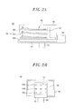
- Fig. 2A is a schematic side view showing an example of the transfer device 50 and Fig. 2B is a front view showing the transfer device 50 viewed in the direction of an arrow 2B.
- the transfer device 50 basically includes a horizontal base 51; and a substrate supporter 52 for supporting one or more target substrates G to be processed, the substrate supporter 52 being forwardly and backwardly moved relative to the horizontal base 51 to transfer the target substrates G.
- the transfer device 50 further includes an elevation/rotation unit 53 for elevating and rotating the horizontal base 51; and a reciprocating unit 54 for forwardly and backwardly reciprocating the substrate supporter 52.
- the transfer device 50 itself is upwardly and downwardly moved and rotated by upwardly and downwardly moving and rotating the horizontal base 51 by the elevation/rotation unit 53.
- the substrate supporter 52 includes a vertical base 55 and a plurality of supporting members 56 (e.g., three supporting members 56a, 56b and 56c in Figs. 2A and 2B ) horizontally extending from the vertical base 55.
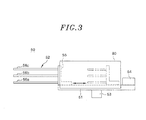
- the vertical base 55 is configured to slide on the horizontal base 51. As shown in Fig. 3 , the substrate supporter 52 is forwardly and backwardly moved relative to the horizontal base 51 by forwardly and backwardly moving the vertical base 55 by the reciprocating unit 54.
- the substrate supporter 52 of the present embodiment includes the plurality of supporting members 56 vertically arranged in multiple stages. Accordingly, the substrate supporter 52 can transfer at a time a plurality of target substrates G to be processed.
- the transfer device 50 including three supporting members 56a, 56b, and 56c can transfer three target substrates G at a time in the present embodiment.
- the transfer device 50 further includes reflecting bodies 80 for reflecting heats, especially infrared rays, radiated from the target substrates G supported in the substrate supporter 52.
- the reflecting bodies 80 are provided at least above and below the target substrates G supported in the substrate supporter 52 located above the horizontal base 51 such that the target substrates G supported by the substrate supporter 52 are moved between the reflecting bodies 80 while being transferred.
- the reflecting bodies 80 are provided at least below the lowermost supporting member 56a and above the uppermost supporting member 56c.
- the target substrates G are transferred while being placed between the reflecting bodies 80 as shown in Fig. 4A . While the target substrates G are transferred, heats radiated from the target substrates G are reflected by the reflecting bodies 80 arranged above and below the substrate supporter 52.
- the reflecting bodies 80 may be provided at sides of the substrate supporter 52 as well as above and below the substrate supporter 52. Accordingly, the reflecting bodies 80 may be arranged to have a tubular shape, and the target substrates G are transferred while being surrounded by the reflecting bodies 80.
- the heats radiated from the target substrates G supported by the substrate supporter 52 are reflected by the reflecting bodies 80.
- a surface of each of the reflection bodies 80 which faces the target substrates G is required to serve as a heat-reflecting surface capable of reflecting at least heat.
- the inner surfaces of the reflecting bodies 80 arranged to have the tubular shape serve as the heat-reflecting surface.
- the heat-reflecting surface is made of a material, e.g., aluminum, capable of easily reflecting infrared rays, and that it is a mirror surface or a polished surface made by polishing a metal material.
- the transfer device 50 of the processing system 1 in accordance with the present embodiment may include the reflecting bodies 80 for reflecting heats radiated from the target substrates G and transfer the target substrates G while the target substrates G are placed between or surrounded by the reflecting bodies 80.
- the heated target substrates G are cooled a little by a gas serving as a heat-transfer medium or the convection of a gas whereas they are significantly cooled by the discharge of the heats radiated from the target substrates G.
- a transfer device having no reflecting body 80 it is possible to significantly suppress the decrease in temperature of the target substrates G while they are transferred, for example, from the preheating chamber 20 to the processing chamber 30a or 30b. Accordingly, by using the transfer device 50 having the reflecting bodies 80, it is possible to reduce a time required to re-heat the target substrates G in the processing chamber 30a or 30b.
- the reflecting bodies 80 are arranged to have a tubular shape such that the substrate supporter 52 is surrounded by the reflecting bodies 80 when the substrate supporter 52 is placed above the horizontal base 51, it is possible to more efficiently suppress the decrease in temperature of the target substrates G while the target substrates G are transferred.
- the transfer device 50 transfers a plurality of, e.g., three or more, target substrates G
- the temperature difference between an uppermost or a lowermost target substrate G and an intermediate target substrate G provided therebetween may be increased.
- the intermediate target substrate G2 radiates a heat, it receives heats radiated from the target substrates G1 and G3 respectively provided below and above the target substrate G2, thereby suppressing the decrease in temperature thereof. Since, however, the lowermost or the uppermost target substrate G1 or G3 has only one adjacent target substrate provided thereabove or therebelow, the temperature of the target substrate G1 or G3 may easily be reduced as compared with the intermediate target substrate G2. Accordingly, when three or more target substrates G are transferred, the temperature difference between the uppermost and the lowermost target substrate G and the intermediate target substrate G may be increased.
- reflecting bodies 80a and 80b are respectively provided above the uppermost target substrate G3 and below the lowermost target substrate G1 as shown in Fig. 6 . Accordingly, even when three or more target substrates G are transferred, it is possible to suppress the increase in temperature difference between the uppermost or the lowermost target substrate G and the intermediate target substrate G, thereby controlling the temperature of each of the target substrates with high accuracy.
- the reflecting bodies 80 are provided at least above and below the substrate supporter 52 in the above-mentioned embodiment, an additional reflecting body for reflecting the heats radiated from the target substrates G may be provided on the surfaces of the supporting members 53 of the substrate supporter 52, for example.
- another additional reflecting body may be provided on the surface of the horizontal base 51.
- the reflecting bodies 80 are arranged to have a tubular shape in the aforementioned embodiment.
- a box-shaped frame may be attached to the horizontal base 51 and the reflecting bodies may be attached on the box-shaped frame.
- the processing system 1 of the aforementioned embodiment transfers and processes three target substrates G at a time.
- the transfer device 50 may have a single supporting member to transfer one target substrate G.
- the transfer device 50 may have two or four or more supporting member to transfer two or four or more, target substrates G.
- the substrate supporter 52 includes the supporting members 56 horizontally extending from the vertical base 55 that slides on the horizontal base 51.
- the substrate supporter 52 is not limited thereto.
- the substrate supporter 52 may have any other configurations for transferring the target substrates G.
- the supporting member 56 may further slide thereon e.
- the present invention is not limited to the transfer type in which the vertical base 55 slides on the horizontal base 51.
- the present invention may use a SCARA transfer type having joints.
- a glass substrate for manufacturing a solar battery or an FPD is used as a target substrate to be processed.
- the target substrate is not limited to the glass substrate.
- a semiconductor wafer or the like may be used.
- the transfer device and the processing system using the same are capable of reducing a time required to re-heat a target substrate to be processed in the processing chamber and controlling the temperature of each of a plurality of substrates with high accuracy even when the substrates are transferred at a time.
Landscapes
- Physics & Mathematics (AREA)
- Nonlinear Science (AREA)
- Engineering & Computer Science (AREA)
- Manufacturing & Machinery (AREA)
- Chemical & Material Sciences (AREA)
- Crystallography & Structural Chemistry (AREA)
- General Physics & Mathematics (AREA)
- Optics & Photonics (AREA)
- Container, Conveyance, Adherence, Positioning, Of Wafer (AREA)
- Chemical Vapour Deposition (AREA)
Abstract
Description
- The present invention relates to a transfer device for transferring a target substrate to be processed, e.g., a large-scale substrate used for a solar battery; and a processing system having the same, for performing a process on the target substrate.
- For the manufacturing process of a solar battery, a flat panel display (FPD) such as a liquid crystal display (LCD), or the like, there has been disclosed a single sheet multi chamber type processing system including a processing chamber in which a predetermined process such as an etching process or a film-forming process is carried out on a large scale glass substrate; and a preheating chamber in which the substrate is preheated to a process temperature (see, e.g., Japanese Patent Application Publication No.
H10-098085 - Such a processing system includes a common transfer chamber having a transfer device for transferring a large scale substrate (target substrate to be processed); a load-lock chamber in which a processed substrate is exchanged with a target substrate to be processed; and the aforementioned preheating chamber and the aforementioned processing chamber. The load-lock chamber, the preheating chamber and the processing chamber are arranged around the common transfer chamber. By the transfer device provided in the common transfer chamber, the target substrate is transferred from the load-lock chamber to the preheating chamber, from the preheating chamber to the processing chamber, and from the processing chamber to the load-lock chamber.
- A processing time can be reduced in the case of preheating a substrate to the process temperature in the preheating chamber before a predetermined process is carried out as compared with the case of heating the substrate to the process temperature in the processing chamber. However, while the substrate is transferred from the preheating chamber to the processing chamber, the temperature of the substrate is decreased. Accordingly, the substrate is required to be re-heated in the processing chamber for a specific period of time.
- Further, in a batch type processing system that processes a plurality of substrates at a time, it is difficult to control the temperature of each of the substrates with high accuracy because the temperature difference between an uppermost substrate or a lowermost substrate and a substrate intermediately provided therebetween is increased.
- In view of the above, the present invention provides a transfer device and a processing system using the same, capable of reducing a time required to re-heat a target substrate to be processed in a processing chamber while controlling the temperature of each of a plurality of substrates with high accuracy even when the substrates are transferred at a time.
- In accordance with a first aspect of the present invention, there is provided a transfer device including: a base; a substrate supporter for supporting one or more target substrates to be processed, the substrate supporter being forwardly and backwardly moved to transfer the target substrates; and reflecting bodies provided at least above and below the substrate supporter, the reflecting bodies serving to reflect heats radiated from the target substrates supported by the substrate supporter.
- In accordance with a second aspect of the present invention, there is provided a processing system including: a common transfer chamber; a preheating chamber, connected to the common transfer chamber, for preheating one or more target substrates to be processed; a load-lock chamber, connected to the common transfer chamber, for switching the target substrates; and the transfer device of the first aspect, provided in the common transfer chamber, for transferring the target substrates.
- The objects and features of the present invention will become apparent from the following description of embodiments, given in conjunction with the accompanying drawings, in which:
-
Fig. 1 is a schematic plan view showing a processing system in accordance with an embodiment of the present invention; -
Fig. 2A is a schematic side view showing an example of a transfer device andFig. 2B is a front view showing the transfer device viewed in a direction of anarrow 2B; -
Fig. 3 shows the transfer device where a substrate supporter is moved forwardly and backwardly relative to a base; -
Figs. 4A and 4B show how target substrates are transferred; -
Fig. 5 shows how heats are radiated from target substrates; -
Fig. 6 shows how heats are radiated from target substrates; and -
Fig. 7 is a side view showing another example of the transfer device. - An embodiment of the present invention will now be described with reference to the accompanying drawings which form a part hereof.
- Further, in the following description and drawings, components having substantially the same configuration and function are denoted by like reference characters.
- Taken for an example of a target substrate to be processed in the present embodiment is a large-scale glass substrate used for manufacturing a solar battery or a flat panel display (FPD) and a processing system that performs a predetermined process, e.g., an etching process or a film-forming process, on the large scale glass substrate is exemplified.
-
Fig. 1 is a schematic plan view showing aprocessing system 1 in accordance with an embodiment of the present invention. - As shown in
Fig. 1 , theprocessing system 1 of the present embodiment includes acommon transfer chamber 10; apreheating chamber 20 for preheating a target substrate G to be processed;processing chambers 30a and 30b for performing an etching process, a film-forming process, or the like on the target substrate G; a load-lock chamber 40 for switching the target substrate G between a substrate container (not shown) disposed in an atmosphere and thecommon transfer chamber 10 that is maintained in a vacuum state; and atransfer device 50 provided in thecommon transfer chamber 10 to transfer the target substrate G. Thepreheating chamber 20, theprocessing chambers 30a and 30b, and the load-lock chamber 40 are arranged around thecommon transfer chamber 10. - The
common transfer chamber 10 is formed in a rectangular shape seen from the top. Thepreheating chamber 20, theprocessing chambers 30a and 30b, the load-lock chamber 40 are connected to side surfaces of thecommon transfer chamber 10 throughgate valves gate valve 64 is provided on the atmospheric side of the load-lock chamber 40. Although thecommon transfer chamber 10 of the present embodiment has the rectangular shape seen from the top as described above, thecommon transfer chamber 10 may have a polygonal (e.g., hexagonal or octagonal) shape, and the preheating chamber, the processing chamber, and the load-lock chamber may additionally be provided. - In the present embodiment, the
common transfer chamber 10, thepreheating chamber 20 and theprocessing chambers 30a and 30b are respectively configured as vacuum chambers and maintained in a predetermined depressurized state. Thepreheating chamber 20 and theprocessing chambers 30a and 30b include therein respective mounting tables 21, 31a, and 31b, each for mounting thereon the target substrate G. Furthermore, the load-lock chamber 40 is provided to transfer the target substrate G between the substrate container (not shown) disposed in the atmosphere and thecommon transfer chamber 10 maintained in a vacuum state, the load-lock chamber 40 serving as a vacuum prechamber that can be switched between the atmospheric state and the depressurized state. - The
substrate processing system 1 is configured to process at a time a plurality of, e.g., three, target substrates G, each of which is horizontally mounted, the target substrates G being arranged in a vertical direction. The target substrates G are loaded together from the external substrate container into the load-lock chamber 40 through thegate valve 64 by a transfer unit (not shown) in the atmosphere. The loaded substrates G are transferred from the load-lock chamber 40 to thecommon transfer chamber 10, from thecommon transfer chamber 10 to thepreheating chamber 20, and from thepreheating chamber 20 to theprocessing chambers 30a or 30b through thegate valves - The target substrates G that have been processed in the
processing chamber 30a or 30b are transferred from theprocessing chamber 30a or 30b to thecommon transfer chamber 10 and from thecommon transfer chamber 10 to the load-lock chamber 40 through thegate valve lock chamber 40. Although theprocessing chambers 30a and 30b perform the same process in the present embodiment, theprocessing chambers 30a and 30b may be configured to perform different processes. In other words, a first process may be carried out in the processing chamber 30a and, successively, a second process may be performed in theprocessing chamber 30b. - The
transfer device 50 serves to transfer the target substrates G between thecommon transfer chamber 10, thepreheating chamber 20, theprocessing chambers 30a and 30b, and the load-lock chamber 40. To that end, thetransfer device 50 is configured to move upwardly, downwardly and rotationally, and forwardly and backwardly between thecommon transfer chamber 10, thepreheating chamber 20, theprocessing chambers 30a and 30b, and the load-lock chamber 40. - The respective components of the
processing system 1 are controlled by a control unit (computer) 70. Thecontrol unit 70 includes aprocess controller 71 having a micro processor. Theprocess controller 71 is connected to auser interface 72 including a keyboard through which an operator inputs a command or the like to manage theprocessing system 1, a display unit for visually displaying an operation status of theprocessing system 1, and the like. Further, theprocess controller 71 is connected to astorage unit 73 which stores therein control programs for realizing various processes performed by theprocessing system 1 under the control of theprocess controller 71; and control programs or recipes for performing predetermined processes performed by theprocessing system 1 under processing conditions. Thestorage unit 73 has a storage medium which stores therein the recipes or the like. - The storage medium may be a hard disk, a semiconductor memory or a portable storage medium such as a CD-ROM, a DVD, a flash memory or the like. If necessary, a certain recipe is retrieved from the
storage unit 73 in response to an instruction from theuser interface 72 or the like and is executed by theprocess controller 71, thereby performing a desired process in theprocessing system 1 under the control of theprocess controller 71. - Next, an example of the processing operation of the
processing system 1 will be described. - First, the
gate valve 64 is opened and a plurality of, e.g., three, target substrates G to be processed are loaded into the load-lock chamber 40 maintained in an atmospheric state by the substrate transfer device (not shown) disposed in the atmosphere. Then, thegate valve 64 is closed, and the inside of the load-lock chamber 40 is set to a depressurized state. Next, thegate valve 63 is opened, and thetransfer device 50 is moved forwardly into the load-lock chamber 40 to take the target substrates G loaded to the load-lock chamber 40. Then, thetransfer device 50 returns to thecommon transfer chamber 10, and thegate valve 63 is closed. - Next, the
transfer device 50 is rotated so as to face thepreheating chamber 20. Then, thegate valve 61 is opened, and thetransfer device 50 is moved forwardly into thepreheating chamber 20 to transfer the target substrates G to thepreheating chamber 20. Then, thetransfer device 50 returns to thecommon transfer chamber 10, and thegate valve 61 is closed. Thereafter, the target substrates G are started to be preheated in the preheatingchamber 20. If the preheating is completed, thegate valve 61 is opened; and thetransfer device 50 is moved forwardly into the preheatingchamber 20 to take the preheated target substrates G. Then, thetransfer device 50 returns to thecommon transfer chamber 10, and thegate valve 61 is closed. - Next, the
transfer device 50 is rotated so as to face theprocessing chamber 30a or 30b. Then, thegate valve transfer device 50 is moved forwardly into theprocessing chamber 30a or 30b to transfer the preheated target substrates G to theprocessing chamber 30a or 30b. Then, thetransfer device 50 returns to thecommon transfer chamber 10, and thegate valve processing chamber 30a or 30b. If the process is completed, thegate valve transfer device 50 is moved forwardly into theprocessing chamber 30a or 30b to take the processed substrates G. Then, thetransfer device 50 returns to thecommon transfer chamber 10, and thegate valve - Next, the
transfer device 50 is rotated so as to face the load-lock chamber 40. Then, thegate valve 63 is opened, and thetransfer device 50 is moved forwardly into the load-lock chamber 40 to transfer the processed substrates G to the load-lock chamber 40. Then, thetransfer device 50 returns to thecommon transfer chamber 10, and thegate valve 63 is closed. Thereafter, the inside of the load-lock chamber 40 is set to the atmospheric state. Then, thegate valve 64 is opened, and the processed substrates G are unloaded from the load-lock chamber 40 by the substrate transfer device (not shown) in the atmosphere. - Next, the
transfer device 50 will be described. -
Fig. 2A is a schematic side view showing an example of thetransfer device 50 andFig. 2B is a front view showing thetransfer device 50 viewed in the direction of anarrow 2B. - As shown in
Figs. 2A and 2B , thetransfer device 50 basically includes ahorizontal base 51; and asubstrate supporter 52 for supporting one or more target substrates G to be processed, thesubstrate supporter 52 being forwardly and backwardly moved relative to thehorizontal base 51 to transfer the target substrates G. - The
transfer device 50 further includes an elevation/rotation unit 53 for elevating and rotating thehorizontal base 51; and areciprocating unit 54 for forwardly and backwardly reciprocating thesubstrate supporter 52. Thetransfer device 50 itself is upwardly and downwardly moved and rotated by upwardly and downwardly moving and rotating thehorizontal base 51 by the elevation/rotation unit 53. - The
substrate supporter 52 includes avertical base 55 and a plurality of supporting members 56 (e.g., three supportingmembers Figs. 2A and 2B ) horizontally extending from thevertical base 55. Thevertical base 55 is configured to slide on thehorizontal base 51. As shown inFig. 3 , thesubstrate supporter 52 is forwardly and backwardly moved relative to thehorizontal base 51 by forwardly and backwardly moving thevertical base 55 by thereciprocating unit 54. - As described above, the
substrate supporter 52 of the present embodiment includes the plurality of supportingmembers 56 vertically arranged in multiple stages. Accordingly, thesubstrate supporter 52 can transfer at a time a plurality of target substrates G to be processed. For example, thetransfer device 50 including three supportingmembers - The
transfer device 50 further includes reflectingbodies 80 for reflecting heats, especially infrared rays, radiated from the target substrates G supported in thesubstrate supporter 52. - The reflecting
bodies 80 are provided at least above and below the target substrates G supported in thesubstrate supporter 52 located above thehorizontal base 51 such that the target substrates G supported by thesubstrate supporter 52 are moved between the reflectingbodies 80 while being transferred. - Specifically, in case that the
substrate supporter 52 includes the supportingmembers bodies 80 are provided at least below the lowermost supportingmember 56a and above theuppermost supporting member 56c. - By providing the reflecting
bodies 80 as described above, the target substrates G are transferred while being placed between the reflectingbodies 80 as shown inFig. 4A . While the target substrates G are transferred, heats radiated from the target substrates G are reflected by the reflectingbodies 80 arranged above and below thesubstrate supporter 52. - Moreover, the reflecting
bodies 80 may be provided at sides of thesubstrate supporter 52 as well as above and below thesubstrate supporter 52. Accordingly, the reflectingbodies 80 may be arranged to have a tubular shape, and the target substrates G are transferred while being surrounded by the reflectingbodies 80. - The heats radiated from the target substrates G supported by the
substrate supporter 52 are reflected by the reflectingbodies 80. To that end, a surface of each of thereflection bodies 80 which faces the target substrates G is required to serve as a heat-reflecting surface capable of reflecting at least heat. In the present embodiment, the inner surfaces of the reflectingbodies 80 arranged to have the tubular shape serve as the heat-reflecting surface. It is preferable that the heat-reflecting surface is made of a material, e.g., aluminum, capable of easily reflecting infrared rays, and that it is a mirror surface or a polished surface made by polishing a metal material. - As such, the
transfer device 50 of theprocessing system 1 in accordance with the present embodiment may include the reflectingbodies 80 for reflecting heats radiated from the target substrates G and transfer the target substrates G while the target substrates G are placed between or surrounded by the reflectingbodies 80. In the depressurized atmosphere, the heated target substrates G are cooled a little by a gas serving as a heat-transfer medium or the convection of a gas whereas they are significantly cooled by the discharge of the heats radiated from the target substrates G. For that reason, as compared with a transfer device having no reflectingbody 80, it is possible to significantly suppress the decrease in temperature of the target substrates G while they are transferred, for example, from the preheatingchamber 20 to theprocessing chamber 30a or 30b. Accordingly, by using thetransfer device 50 having the reflectingbodies 80, it is possible to reduce a time required to re-heat the target substrates G in theprocessing chamber 30a or 30b. - As described above, it is sufficient to provide the reflecting
bodies 80 above and below thesubstrate supporter 52. However, in case that the reflectingbodies 80 are arranged to have a tubular shape such that thesubstrate supporter 52 is surrounded by the reflectingbodies 80 when thesubstrate supporter 52 is placed above thehorizontal base 51, it is possible to more efficiently suppress the decrease in temperature of the target substrates G while the target substrates G are transferred. - Moreover, the following benefits can be obtained by the
transfer device 50 included in theprocessing system 1 of the present embodiment. - For example, when the
transfer device 50 transfers a plurality of, e.g., three or more, target substrates G, the temperature difference between an uppermost or a lowermost target substrate G and an intermediate target substrate G provided therebetween may be increased. - As shown in
Fig. 5 , while the intermediate target substrate G2 radiates a heat, it receives heats radiated from the target substrates G1 and G3 respectively provided below and above the target substrate G2, thereby suppressing the decrease in temperature thereof. Since, however, the lowermost or the uppermost target substrate G1 or G3 has only one adjacent target substrate provided thereabove or therebelow, the temperature of the target substrate G1 or G3 may easily be reduced as compared with the intermediate target substrate G2. Accordingly, when three or more target substrates G are transferred, the temperature difference between the uppermost and the lowermost target substrate G and the intermediate target substrate G may be increased. - On the other hand, in the
transfer device 50 of theprocessing system 1 in accordance with the present embodiment, reflectingbodies Fig. 6 . Accordingly, even when three or more target substrates G are transferred, it is possible to suppress the increase in temperature difference between the uppermost or the lowermost target substrate G and the intermediate target substrate G, thereby controlling the temperature of each of the target substrates with high accuracy. - Although the embodiment of the present invention has been described above, the present invention is limited to the embodiment, and various modifications may be made. In other words, the present invention may be implemented by other embodiments than the aforementioned embodiment.
- For example, although the reflecting
bodies 80 are provided at least above and below thesubstrate supporter 52 in the above-mentioned embodiment, an additional reflecting body for reflecting the heats radiated from the target substrates G may be provided on the surfaces of the supportingmembers 53 of thesubstrate supporter 52, for example. - Further, another additional reflecting body may be provided on the surface of the
horizontal base 51. - In addition, the reflecting
bodies 80 are arranged to have a tubular shape in the aforementioned embodiment. However, a box-shaped frame may be attached to thehorizontal base 51 and the reflecting bodies may be attached on the box-shaped frame. - Further, the
processing system 1 of the aforementioned embodiment transfers and processes three target substrates G at a time. The present invention, however, is not limited thereto. For example, as shown inFig. 7 , thetransfer device 50 may have a single supporting member to transfer one target substrate G. Alternatively, thetransfer device 50 may have two or four or more supporting member to transfer two or four or more, target substrates G. - Moreover, in the above-mentioned embodiment, the
substrate supporter 52 includes the supportingmembers 56 horizontally extending from thevertical base 55 that slides on thehorizontal base 51. However, thesubstrate supporter 52 is not limited thereto. Thesubstrate supporter 52 may have any other configurations for transferring the target substrates G. For example, the supportingmember 56 may further slide thereon e. Further, the present invention is not limited to the transfer type in which thevertical base 55 slides on thehorizontal base 51. The present invention may use a SCARA transfer type having joints. - Finally, a glass substrate for manufacturing a solar battery or an FPD is used as a target substrate to be processed. The target substrate is not limited to the glass substrate. A semiconductor wafer or the like may be used.
- In accordance with the embodiments of the present invention, the transfer device and the processing system using the same are capable of reducing a time required to re-heat a target substrate to be processed in the processing chamber and controlling the temperature of each of a plurality of substrates with high accuracy even when the substrates are transferred at a time.
- While the invention has been shown and described with respect to the embodiments, it will be understood by those skilled in the art that various changes and modifications may be made without departing from the scope of the invention as defined in the following claims.
Claims (7)
- A transfer device comprising:a base;a substrate supporter for supporting one or more target substrates to be processed, the substrate supporter being forwardly and backwardly moved to transfer the target substrates; andreflecting bodies provided at least above and below the substrate supporter, the reflecting bodies serving to reflect heats radiated from the target substrates supported by the substrate supporter.
- The transfer device of claim 1, wherein the substrate supporter has a plurality of stages between the reflecting bodies.
- The transfer device of claim 1 or 2, wherein the reflecting bodies are arranged to have a tubular shape such that the substrate supporter is surrounded by the reflecting bodies.
- The transfer device of any one of claims 1 to 3, wherein at least a surface of each of the reflecting bodies which faces the target substrate serves as a heat-reflecting surface for reflecting a heat.
- The transfer device of any one of claims 1 to 4, further comprising another reflecting body provided on a surface of the substrate support to reflect the heat radiated from the target substrate.
- The transfer device of any one of claims 1 to 5, further comprising another reflecting body provided on a surface of the base to reflect the heat radiated from the target substrate.
- A processing system comprising:a common transfer chamber;a preheating chamber, connected to the common transfer chamber, for preheating one or more target substrates to be processed;a processing chamber, connected to the common transfer chamber, for processing the target substrates;a load-lock chamber, connected to the common transfer chamber, for switching the target substrates; andthe transfer device of any one of claims 1 to 6, provided in the common transfer chamber, for transferring the target substrates,
Applications Claiming Priority (1)
| Application Number | Priority Date | Filing Date | Title |
|---|---|---|---|
| JP2009178870A JP2011035103A (en) | 2009-07-31 | 2009-07-31 | Carrier device and processing system |
Publications (2)
| Publication Number | Publication Date |
|---|---|
| EP2282330A2 true EP2282330A2 (en) | 2011-02-09 |
| EP2282330A3 EP2282330A3 (en) | 2012-01-11 |
Family
ID=42983517
Family Applications (1)
| Application Number | Title | Priority Date | Filing Date |
|---|---|---|---|
| EP10171425A Withdrawn EP2282330A3 (en) | 2009-07-31 | 2010-07-30 | Transfer device and processing system having the same |
Country Status (6)
| Country | Link |
|---|---|
| US (1) | US20110027049A1 (en) |
| EP (1) | EP2282330A3 (en) |
| JP (1) | JP2011035103A (en) |
| KR (1) | KR101257991B1 (en) |
| CN (1) | CN101989561A (en) |
| TW (1) | TW201118024A (en) |
Families Citing this family (3)
| Publication number | Priority date | Publication date | Assignee | Title |
|---|---|---|---|---|
| CN102177003B (en) * | 2008-10-07 | 2015-04-22 | 川崎重工业株式会社 | Substrate transfer robot and system |
| US8388094B2 (en) | 2009-07-31 | 2013-03-05 | Zamtec Ltd | Wide format printer with input roller and movable media engagement output |
| JP2014038990A (en) * | 2012-08-20 | 2014-02-27 | Tokyo Electron Ltd | Substrate conveyance device and substrate processing system |
Citations (1)
| Publication number | Priority date | Publication date | Assignee | Title |
|---|---|---|---|---|
| JPH1098085A (en) | 1996-09-19 | 1998-04-14 | Hitachi Ltd | Plasma processing apparatus and thin film transistor manufacturing method |
Family Cites Families (32)
| Publication number | Priority date | Publication date | Assignee | Title |
|---|---|---|---|---|
| JPH081923B2 (en) * | 1991-06-24 | 1996-01-10 | ティーディーケイ株式会社 | Clean transfer method and device |
| TW245823B (en) * | 1992-10-05 | 1995-04-21 | Tokyo Electron Co Ltd | |
| JPH0786375A (en) * | 1993-09-17 | 1995-03-31 | Dainippon Screen Mfg Co Ltd | Substrate transfer device |
| US5616208A (en) * | 1993-09-17 | 1997-04-01 | Tokyo Electron Limited | Vacuum processing apparatus, vacuum processing method, and method for cleaning the vacuum processing apparatus |
| JPH07142408A (en) * | 1993-11-12 | 1995-06-02 | Nissin Electric Co Ltd | Substrate processing system |
| US5664925A (en) * | 1995-07-06 | 1997-09-09 | Brooks Automation, Inc. | Batchloader for load lock |
| JP3543887B2 (en) * | 1995-11-30 | 2004-07-21 | 大日本スクリーン製造株式会社 | Substrate processing equipment |
| JPH10284569A (en) * | 1997-04-08 | 1998-10-23 | Toshiba Mach Co Ltd | Wafer conveyer |
| US6242718B1 (en) * | 1999-11-04 | 2001-06-05 | Asm America, Inc. | Wafer holder |
| KR100352765B1 (en) * | 1999-12-01 | 2002-09-16 | 삼성전자 주식회사 | Heat treatment apparatus for manufacturing semiconductor |
| JP4346765B2 (en) * | 2000-01-04 | 2009-10-21 | 株式会社アルバック | Substrate transfer robot |
| US6500737B1 (en) * | 2000-06-08 | 2002-12-31 | Wafermasters, Inc. | System and method for providing defect free rapid thermal processing |
| JP3983481B2 (en) * | 2001-01-31 | 2007-09-26 | 東京エレクトロン株式会社 | Substrate processing apparatus and substrate transfer method in substrate processing apparatus |
| JP2002289669A (en) * | 2001-03-28 | 2002-10-04 | Hitachi Kokusai Electric Inc | Substrate processing equipment |
| JP2002343847A (en) * | 2001-05-18 | 2002-11-29 | Nec Yamaguchi Ltd | Wafer conveying apparatus |
| JP3783075B2 (en) * | 2001-12-13 | 2006-06-07 | 東京エレクトロン株式会社 | Probe device and loader device |
| JP2003188229A (en) * | 2001-12-18 | 2003-07-04 | Hitachi Kasado Eng Co Ltd | Wafer manufacturing system and wafer manufacturing method |
| US6709470B2 (en) * | 2002-04-15 | 2004-03-23 | Wafermasters, Inc. | Benchtop processing |
| CN100461363C (en) * | 2004-12-10 | 2009-02-11 | 株式会社爱发科 | Handling manipulator and handling device |
| JP2006185974A (en) * | 2004-12-27 | 2006-07-13 | Kyocera Corp | Firing furnace, method for firing object to be processed using the same, and method for producing solar cell element |
| JP2006237256A (en) * | 2005-02-24 | 2006-09-07 | Ulvac Japan Ltd | Circuit board transfer hand |
| KR20070029032A (en) * | 2005-09-08 | 2007-03-13 | 주성엔지니어링(주) | Mobile transfer chamber and substrate processing apparatus including the same |
| US20070051314A1 (en) * | 2005-09-08 | 2007-03-08 | Jusung Engineering Co., Ltd. | Movable transfer chamber and substrate-treating apparatus including the same |
| JP4614455B2 (en) * | 2006-04-19 | 2011-01-19 | 東京エレクトロン株式会社 | Substrate transfer processing equipment |
| JP2008103707A (en) * | 2006-09-22 | 2008-05-01 | Hitachi Kokusai Electric Inc | Substrate processing apparatus and semiconductor device manufacturing method |
| JP5192719B2 (en) * | 2007-04-12 | 2013-05-08 | 株式会社アルバック | Heating apparatus and substrate processing apparatus |
| JP4908306B2 (en) * | 2007-05-10 | 2012-04-04 | 株式会社ダイヘン | Transport device |
| US7496423B2 (en) * | 2007-05-11 | 2009-02-24 | Applied Materials, Inc. | Method of achieving high productivity fault tolerant photovoltaic factory with batch array transfer robots |
| JP5050761B2 (en) * | 2007-10-03 | 2012-10-17 | 東京エレクトロン株式会社 | Processing system for object to be processed and heat treatment method for object to be processed |
| WO2009054064A1 (en) * | 2007-10-26 | 2009-04-30 | Shimadzu Corporation | Substrate loading apparatus |
| TW201013760A (en) * | 2008-09-17 | 2010-04-01 | Inotera Memories Inc | A wafer base clean room and a method of using the wafer base clean room |
| KR101543273B1 (en) * | 2008-10-27 | 2015-08-12 | 주성엔지니어링(주) | Appratus for treatmenting substrate |
-
2009
- 2009-07-31 JP JP2009178870A patent/JP2011035103A/en not_active Ceased
-
2010
- 2010-07-20 CN CN201010233776XA patent/CN101989561A/en active Pending
- 2010-07-29 KR KR1020100073489A patent/KR101257991B1/en not_active Expired - Fee Related
- 2010-07-30 TW TW099125424A patent/TW201118024A/en unknown
- 2010-07-30 EP EP10171425A patent/EP2282330A3/en not_active Withdrawn
- 2010-07-30 US US12/847,365 patent/US20110027049A1/en not_active Abandoned
Patent Citations (1)
| Publication number | Priority date | Publication date | Assignee | Title |
|---|---|---|---|---|
| JPH1098085A (en) | 1996-09-19 | 1998-04-14 | Hitachi Ltd | Plasma processing apparatus and thin film transistor manufacturing method |
Also Published As
| Publication number | Publication date |
|---|---|
| EP2282330A3 (en) | 2012-01-11 |
| JP2011035103A (en) | 2011-02-17 |
| US20110027049A1 (en) | 2011-02-03 |
| TW201118024A (en) | 2011-06-01 |
| KR20110013307A (en) | 2011-02-09 |
| CN101989561A (en) | 2011-03-23 |
| KR101257991B1 (en) | 2013-04-24 |
Similar Documents
| Publication | Publication Date | Title |
|---|---|---|
| US7836845B2 (en) | Substrate carrying and processing apparatus | |
| JP5478280B2 (en) | Substrate heating apparatus, substrate heating method, and substrate processing system | |
| US8469346B2 (en) | Substrate mounting mechanism and substrate processing apparatus using same | |
| CN101266924B (en) | Substrate processing apparatus, substrate processing method | |
| US9803926B2 (en) | Support mechanism and substrate processing apparatus | |
| JP5106331B2 (en) | Method for lowering temperature of substrate mounting table, computer-readable storage medium, and substrate processing system | |
| EP2282331B1 (en) | Substrate position alignment mechanism | |
| TWI753655B (en) | Dual load lock chamber and processing system including the dual load lock chamber | |
| US7371998B2 (en) | Thermal wafer processor | |
| US20150243490A1 (en) | Substrate processing apparatus and substrate processing method | |
| WO2003071600A1 (en) | Substrate support mechanism in semiconductor processing system | |
| JP2009206270A (en) | Load lock apparatus and substrate cooling method | |
| EP2282330A2 (en) | Transfer device and processing system having the same | |
| TW201624599A (en) | Substrate transfer method and processing system | |
| JP5496837B2 (en) | Cooling method, cooling device, and computer-readable storage medium for workpiece | |
| JP2011174108A (en) | Cooling apparatus and substrate processing apparatus having the same | |
| JP2013009007A (en) | Substrate transfer method in substrate processing apparatus | |
| US9679794B2 (en) | Spacer, spacer transferring method, processing method and processing apparatus | |
| CN104952727A (en) | Device for heat treatment | |
| JP6680895B2 (en) | Substrate processing apparatus, semiconductor device manufacturing method, and program | |
| JP2011117085A (en) | Load-lock chamber and thin film forming apparatus having the same | |
| JP2002020868A (en) | Thin film forming equipment |
Legal Events
| Date | Code | Title | Description |
|---|---|---|---|
| PUAI | Public reference made under article 153(3) epc to a published international application that has entered the european phase |
Free format text: ORIGINAL CODE: 0009012 |
|
| 17P | Request for examination filed |
Effective date: 20100730 |
|
| AK | Designated contracting states |
Kind code of ref document: A2 Designated state(s): AL AT BE BG CH CY CZ DE DK EE ES FI FR GB GR HR HU IE IS IT LI LT LU LV MC MK MT NL NO PL PT RO SE SI SK SM TR |
|
| AX | Request for extension of the european patent |
Extension state: BA ME RS |
|
| PUAL | Search report despatched |
Free format text: ORIGINAL CODE: 0009013 |
|
| AK | Designated contracting states |
Kind code of ref document: A3 Designated state(s): AL AT BE BG CH CY CZ DE DK EE ES FI FR GB GR HR HU IE IS IT LI LT LU LV MC MK MT NL NO PL PT RO SE SI SK SM TR |
|
| AX | Request for extension of the european patent |
Extension state: BA ME RS |
|
| RIC1 | Information provided on ipc code assigned before grant |
Ipc: H01L 21/677 20060101AFI20111207BHEP |
|
| STAA | Information on the status of an ep patent application or granted ep patent |
Free format text: STATUS: THE APPLICATION HAS BEEN WITHDRAWN |
|
| 18W | Application withdrawn |
Effective date: 20140408 |