EP2270881A2 - Light-emitting element and a production method therefor - Google Patents
Light-emitting element and a production method therefor Download PDFInfo
- Publication number
- EP2270881A2 EP2270881A2 EP09739001A EP09739001A EP2270881A2 EP 2270881 A2 EP2270881 A2 EP 2270881A2 EP 09739001 A EP09739001 A EP 09739001A EP 09739001 A EP09739001 A EP 09739001A EP 2270881 A2 EP2270881 A2 EP 2270881A2
- Authority
- EP
- European Patent Office
- Prior art keywords
- layer
- conductivity
- type semiconductor
- light emitting
- emitting device
- Prior art date
- Legal status (The legal status is an assumption and is not a legal conclusion. Google has not performed a legal analysis and makes no representation as to the accuracy of the status listed.)
- Granted
Links
Images



Classifications
-
- H—ELECTRICITY
- H10—SEMICONDUCTOR DEVICES; ELECTRIC SOLID-STATE DEVICES NOT OTHERWISE PROVIDED FOR
- H10H—INORGANIC LIGHT-EMITTING SEMICONDUCTOR DEVICES HAVING POTENTIAL BARRIERS
- H10H20/00—Individual inorganic light-emitting semiconductor devices having potential barriers, e.g. light-emitting diodes [LED]
- H10H20/80—Constructional details
- H10H20/81—Bodies
- H10H20/816—Bodies having carrier transport control structures, e.g. highly-doped semiconductor layers or current-blocking structures
- H10H20/8162—Current-blocking structures
-
- H—ELECTRICITY
- H10—SEMICONDUCTOR DEVICES; ELECTRIC SOLID-STATE DEVICES NOT OTHERWISE PROVIDED FOR
- H10H—INORGANIC LIGHT-EMITTING SEMICONDUCTOR DEVICES HAVING POTENTIAL BARRIERS
- H10H20/00—Individual inorganic light-emitting semiconductor devices having potential barriers, e.g. light-emitting diodes [LED]
- H10H20/01—Manufacture or treatment
- H10H20/011—Manufacture or treatment of bodies, e.g. forming semiconductor layers
- H10H20/018—Bonding of wafers
Definitions
- the present disclosure relates to a light emitting device and a method for manufacturing the same.
- LEDs light emitting diodes
- An LED is a device that converts an electric signal into light by using characteristics of compound semiconductors.
- An LED has a stacked structure with a semiconductor layer of a first conductivity type, an active layer, and a semiconductor layer of a second conductivity type, and emits light from the active layer when a voltage is applied.
- the first conductivity-type semiconductor layer may be an n-type semiconductor layer and the second conductivity-type semiconductor layer may be a p-type semiconductor layer, and vice versa.
- electric current may not flow in a wide area and may flow with concentration on a lower side of the first electrode layer. If the electric current flows with concentration on a specific region, an operating voltage may increase to lower the intensity of light, thus degrading the reliability of the light emitting device.
- Embodiments provide a light emitting device having a new structure, and a method for manufacturing the same.
- Embodiments also provide a light emitting device having improved light extraction efficiency, and a method for manufacturing the same.
- Embodiments also provide a light emitting device capable of suppressing electric current from flowing with concentration on a specific region, and a method for manufacturing the same.
- Embodiments also provide a light emitting device capable of operating a stable driving voltage, and a method for manufacturing the same.
- a light emitting device comprises: a second electrode layer; a second conductivity-type semiconductor layer on the second electrode layer; a current blocking layer comprising an oxide of the second conductivity-type semiconductor layer; an active layer on the second conductivity-type semiconductor layer; a first conductivity-type semiconductor layer on the active layer; and a first electrode layer on the first conductivity-type semiconductor layer.
- a light emitting device comprises: a second electrode layer; a second conductivity-type semiconductor layer on the second electrode layer; an active layer on the second conductivity-type semiconductor layer; a first conductivity-type semiconductor layer on the active layer; a current blocking layer in the first conductivity-type semiconductor layer; and a first electrode layer on the first conductivity-type semiconductor layer.
- Embodiments can provide a light emitting device having a new structure, and a method for manufacturing the same.
- Embodiments also can provide a light emitting device having improved light extraction efficiency, and a method for manufacturing the same.
- Embodiments also can provide a light emitting device capable of suppressing electric current from flowing with concentration on a specific region, and a method for manufacturing the same.
- Embodiments also can provide a light emitting device capable of operating a stable driving voltage, and a method for manufacturing the same.
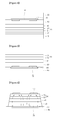
- Figs. 1 to 6 are sectional views explaining a light emitting device and a method for manufacturing the same according to a first embodiment.
- the light emitting device includes a second electrode layer 90, an ohmic contact layer 80 on the second electrode layer 90, a second conductivity-type semiconductor layer 50 on the ohmic contact layer 80, an active layer 40, a first conductivity-type semiconductor layer 30, and a first electrode 100 on the first conductivity-type semiconductor layer 30.
- a current blocking layer 70 for changing a current path is disposed on the second conductivity-type semiconductor layer 50.
- a bottom surface and a side surface of the ohmic contact layer 80 may be in contact with the second electrode layer 90.
- a top surface of the ohmic contact layer 80 and a top surface of the second electrode layer 90 may be disposed on the same horizontal plane.
- the first electrode layer 100 and the ohmic contact layer 80 are disposed in a vertical direction.
- the first electrode layer 100 and the second electrode layer 90 may be disposed in a vertical direction. That is, at least portions of the first electrode layer 100 and the ohmic contact layer 80 or the second electrode layer 90 may be disposed on the same vertical plane.
- the current blocking layer 70 is disposed inside the second conductivity-type semiconductor layer 50.
- the current blocking layer 70 may be disposed at a boundary between the second conductivity-type semiconductor layer 50 and the ohmic contact layer 80.
- a top surface and a side surface of the current blocking layer 70 may be in contact with the second conductivity-type semiconductor layer 50, and a bottom surface of the current blocking layer 70 may be in contact with the ohmic contact layer 80.
- the current blocking layer 70 may be formed of a material having an insulating characteristic, and the current blocking layer 70 may be formed of oxide by oxidizing the second conductivity-type semiconductor layer 50.
- the current blocking layer 70 may be formed of Ga x O y , which is formed by a plasma oxidation process, and may have a thickness of about 10 nm to about 100 nm.
- the current flowing from the ohmic contact layer 80 to the first electrode layer 100 does not concentrate on the lower side of the first electrode layer 100, and flows in a wide area over the first conductivity-type semiconductor layer 30.
- the light emitting device can operate at a stable operating voltage and the light emission efficiency can be improved.
- the first conductivity-type semiconductor layer 30 may include a first nitride layer 31 and a second nitride layer 32.
- the first nitride layer 31 may be formed of a medium layer having a lower refractive index than the second nitride layer 32.
- the second nitride layer 32 may be formed of a medium layer having a higher refractive index than the first nitride layer 31.
- the first nitride layer 31 may be formed of Al x Ga 1-x N (0 ⁇ x ⁇ 1), for example, n-AlGaN or n-AlN, and the second layer 32 may be formed of n-GaN.
- the refractive index of GaN is about 2.44 and the refractive index of AlGaN or AIN is about 2.12 to about 2.44.
- the refractive index of AlGaN changes to about 2.12 to about 2.44 according to a composition ratio of Al to Ga.
- the refractive index becomes lower, thus increasing the light extraction efficiency.
- the first conductivity-type semiconductor layer 30 includes the first nitride layer 31 and the second nitride layer 32, light that is emitted from the active layer 40 and incident onto the second nitride layer 32 can be effectively extracted through the first nitride layer 31 to the outside. Consequently, the light emission efficiency of the light emitting device can be improved.
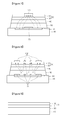
- Fig. 7 is a sectional view of a light emitting device according to a second embodiment
- Fig. 8 is a sectional view of a light emitting device according to a third embodiment.
- the current blocking layer 70 is modified in the position, size and number.
- the position of the first electrode layer 100 may be changed according to the position, size and number of the current blocking layer 70.
- the current blocking layer 70 may be disposed in a central region of the bottom surface of the second conductivity-type semiconductor layer 50, or a region other than the central region. Furthermore, the current blocking layer 70 may have at least two different sizes.
- an undoped GaN layer 20 a first conductivity-type semiconductor layer 30, an active layer 40, and a second conductivity-type semiconductor layer 50 are formed on a substrate 10.
- a buffer layer (not shown) may be further formed between the substrate 10 and the undoped GaN layer 20.
- the substrate 10 may be formed of at least one of sapphire (Al 2 O 3 ), Si, SiC, GaAs, ZnO, or MgO.
- the buffer layer may include a multi-layer with a stacked structure such as AlInN/GaN, In x Ga 1-x N/GaN, and Al x InyGa 1-x-y N/In x Ga 1-x N/GaN.
- the buffer layer may be grown by injecting trimethylgallium (TMGa), trimethylindium (TMIn), and trimethylaluminum (TMAI) into the chamber together with hydrogen gas and ammonia gas.
- the undoped GaN layer 20 may be grown by injecting trimethylgallium (TMGa) into the chamber together with hydrogen gas and ammonia gas.
- TMGa trimethylgallium
- the first conductivity-type semiconductor layer 30 may be a nitride semiconductor layer doped with impurity ions of the first conductivity type, and the first conductivity-type semiconductor layer 30 may include a first nitride layer 31 having a low refractive index and a second nitride layer 32 having a high refractive index.
- the first conductivity-type semiconductor layer 30 may be a semiconductor layer doped with n-type impurity ions.
- the first conductivity-type semiconductor layer 30 may be grown by injecting trimethylgallium (TMGa), trimethylaluminum (TMAI), and silane gas (SiN 4 ) containing n-type impurities (for example, Si) into the chamber together with hydrogen gas and ammonia gas.
- TMGa trimethylgallium
- TMAI trimethylaluminum
- SiN 4 silane gas
- the active layer 40 and the second conductivity-type semiconductor layer 50 are formed on the first conductivity-type semiconductor layer 30.
- the active layer 40 may be formed in a single quantum well structure or a multi-quantum well structure.
- the active layer 40 may be formed in a stacked structure of an InGaN well layer/a GaN barrier layer.
- the second conductivity-type semiconductor layer 50 may be a nitride semiconductor layer doped with impurity ions of the second conductivity type.
- the second conductivity-type semiconductor layer 50 may be a semiconductor layer doped with p-type impurity ions.
- the second conductivity-type semiconductor layer 50 may be grown by injecting bis(ethylcyclopentadienyl)magnesium (EtCp 2 Mg) ⁇ Mg(C 2 H 5 C 5 H 4 ) 2 ⁇ into the chamber together with hydrogen gas and ammonia gas.
- a mask 60 is formed on the second conductivity-type semiconductor layer 50, and a current blocking layer 70 is selectively formed by O 2 plasma.
- the current blocking layer 70 may be formed of oxide, for example, Ga x O y .
- the current blocking layer 70 may be represented by the following chemical formula. 4GaN+3O 2 ⁇ 2Ga 2 O 3 +2N 2
- the current blocking layer 70 may be formed as illustrated in Fig. 7 or 8 according to patterns of the mask 60.
- the mask 60 is removed.
- an ohmic contact layer 80 and a second electrode layer 90 are formed on the second conductivity-type semiconductor layer 50 and the current blocking layer 70.
- the ohmic contact layer 80 may include a transparent electrode layer.
- the ohmic contact layer 80 may be formed of at least one of indium tin oxide (ITO), ZnO, RuO x , TiO x , or IrO x .
- the ohmic contact layer 80 may include at least one of a reflective layer and an adhesive layer.
- the second electrode layer 90 may be formed of at least one of copper (Cu), titan (Ti), chrome (Cr), nickel (Ni), aluminum (Al), platinum (Pt), gold (Au), or a conductive substrate.
- the substrate 10 and the undoped GaN layer 20 are removed from the structure of Fig. 4 . If the buffer layer has been formed, the buffer layer is also removed.
- an isolation etching process for chip separation is performed on the structure of Fig. 5 .
- a first electrode layer 100 is formed on the first conductivity-type semiconductor layer 30.
- the first electrode layer 100 may be formed of at least one of copper (Cu), titan (Ti), chrome (Cr), nickel (Ni), aluminum (Al), platinum (Pt), or gold (Au).
- the light emitting device of Fig. 6 can be manufactured.
- Figs. 9 to 15 are sectional views explaining a light emitting device and a method for manufacturing the same according to a fourth embodiment.
- the light emitting device includes a second electrode layer 90, an ohmic contact layer 80 on the second electrode layer 90, a second conductivity-type semiconductor layer 50 on the ohmic contact layer 80, an active layer 40, a first conductivity-type semiconductor layer 30, and a first electrode 100 on the first conductivity-type semiconductor layer 30. Also, a current blocking layer 70 for changing a current path is disposed on the first conductivity-type semiconductor layer 30.
- a bottom surface and a side surface of the ohmic contact layer 80 may be in contact with the second electrode layer 90.
- a top surface of the ohmic contact layer 80 and a top surface of the second electrode layer 90 may be disposed on the same horizontal plane.
- the first electrode layer 100 and the ohmic contact layer 80 are disposed in a vertical direction.
- the first electrode layer 100 and the second electrode layer 90 may be disposed in a vertical direction. That is, at least a portion of the first electrode layer 100 and the ohmic contact layer 80 or the second electrode layer 90 may be disposed on the same vertical plane.
- the current blocking layer 70 is disposed inside the first conductivity-type semiconductor layer 30 under the first electrode layer 100.
- the current blocking layer 70 is formed of an insulating material.
- the current blocking layer 70 may be formed of at least one of SiO 2 , SiN x , TiO 2 , Ta 2 O 3 , SiOn, and SiCN.
- the current flowing from the ohmic contact layer 80 to the first electrode layer 100 does not concentrate on the lower side of the first electrode layer 100, and flows in a wide area over the first conductivity-type semiconductor layer 30.
- the light emitting device can operate at a stable operating voltage and the light emission efficiency can be improved.
- the first conductivity-type semiconductor layer 30 may include a first nitride layer 31 and a second nitride layer 32.
- the first nitride layer 31 may be formed of a medium layer having a lower refractive index than the second nitride layer 32.
- the second nitride layer 32 may be formed of a medium layer having a higher refractive index than the first nitride layer 31.
- the current blocking layer 70 is formed in the second nitride layer 32.
- the first nitride layer 31 may be formed of Al x Ga 1-x N (0 ⁇ x ⁇ 1), for example, n-AlGaN or n-AlN, and the second layer 32 may be formed of n-GaN.
- the refractive index of GaN is about 2.44 and the refractive index of AlGaN or AIN is about 2.12 to about 2.44.
- the refractive index of AlGaN changes to about 2.12 to about 2.44 according to a composition ratio of Al to Ga.
- the refractive index becomes lower, thus increasing the light extraction efficiency.
- the first conductivity-type semiconductor layer 30 includes the first nitride layer 31 and the second nitride layer 32, light that is emitted from the active layer 40 and incident onto the second nitride layer 32 can be effectively extracted through the first nitride layer 31 to the outside. Consequently, the light emission efficiency of the light emitting device can be improved.
- Fig. 16 is a sectional view of a light emitting device according to a fifth embodiment.
- the fundamental characteristics of the light emitting device of Fig. 16 are similar to those of the light emitting device of Fig. 15 . However, in the light emitting device of Fig. 16 , the current blocking layer 70 is partially provided in plurality.
- the first conductivity-type semiconductor layer 30 can be grown more easily.
- Fig. 17 is a plan view of the current blocking layer illustrated in Fig. 15
- Fig. 18 is a plan view of the current blocking layer illustrated in Fig. 16 .
- the first conductivity-type semiconductor layer 30 is also grown on the current blocking layer 70.
- the current blocking layer 70 is divided into a plurality of layers and spaced apart from one another, the first conductivity-type semiconductor layer 30 can be grown between the current blocking layers 70.
- an undoped GaN layer 20 and a first conductivity-type semiconductor layer 30 are formed on a substrate 10.
- a buffer layer (not shown) may be further formed between the substrate 10 and the undoped GaN layer 20.
- the substrate 10 may be formed of at least one of sapphire (Al 2 O 3 ), Si, SiC, GaAs, ZnO, or MgO.
- the buffer layer may include a multi-layer with a stacked structure such as AlInN/GaN, In x Ga 1-x N/GaN, and Al x In y Ga 1-x-y N/In x Ga 1-x N/GaN.
- the buffer layer may be grown by injecting trimethylgallium (TMGa), trimethylindium (TMIn), and trimethylaluminum (TMAI) into the chamber together with hydrogen gas and ammonia gas.
- the undoped GaN layer 20 may be grown by injecting trimethylgallium (TMGa) into the chamber together with hydrogen gas and ammonia gas.
- TMGa trimethylgallium
- the first conductivity-type semiconductor layer 30 may be a nitride semiconductor layer doped with impurity ions of the first conductivity type, and the first conductivity-type semiconductor layer 30 may include a first nitride layer 31 having a low refractive index and a second nitride layer 32 having a high refractive index.
- the first conductivity-type semiconductor layer 30 may be a semiconductor layer doped with n-type impurity ions.
- the first conductivity-type semiconductor layer 30 may be grown by injecting trimethylgallium (TMGa), trimethylaluminum (TMAI), and silane gas (SiN 4 ) containing n-type impurities (for example, Si) into the chamber together with hydrogen gas and ammonia gas.
- TMGa trimethylgallium
- TMAI trimethylaluminum
- SiN 4 silane gas
- the first nitride layer 31 is formed on the undoped GaN layer 20, and the second nitride layer 32 is grown on the first nitride layer 31 to a predetermined thickness.
- a mask (not shown) is formed on the second nitride layer 32, and a current blocking layer 70 is formed of an insulating material.
- the current blocking layer 70 may be formed of at least one of SiO 2 , SiN x , TiO 2 , Ta 2 O 3 , SiON, and SiCN.
- the current blocking layer 70 when it is formed of SiO 2 , it can be formed through a CVD process by injecting silicon-containing gas such as SiH 4 or Si 2 H 6 and oxygen-containing gas such as N 2 O, O 2 or O 3 .
- the current blocking layer 70 may be formed as illustrated in Figs. 10 and 17 or Figs. 16 and 18 according to the pattern shapes of the mask (not shown).
- the mask (not shown) is removed, and the second nitride layer 30 is additionally grown. As the second nitride layer 32 is additionally grown, the current blocking layer 70 is buried within the second nitride layer 32.
- An active layer 40 and a semiconductor layer 50 of a second conductivity type are formed on the first conductivity-type semiconductor layer 30.
- the active layer 40 may be formed in a single quantum well structure or a multi-quantum well structure.
- the active layer 40 may be formed in a stacked structure of an InGaN well layer/a GaN barrier layer.
- the second conductivity-type semiconductor layer 50 may be a nitride semiconductor layer doped with impurity ions of the second conductivity type.
- the second conductivity-type semiconductor layer 50 may be a semiconductor layer doped with p-type impurity ions.
- the second conductivity-type semiconductor layer 50 may be grown by injecting bis(ethylcyclopentadienyl)magnesium (EtCp 2 Mg) ⁇ Mg(C 2 H 5 C 5 H 4 ) 2 ⁇ into the chamber together with hydrogen gas and ammonia gas.
- an ohmic contact layer 80 and a second electrode layer 90 are formed on the second conductivity-type semiconductor layer 50.
- the ohmic contact layer 80 may include a transparent electrode layer.
- the ohmic contact layer 80 may be formed of at least one of indium tin oxide (ITO), ZnO, RuO x , TiO x , or IrO x .
- the ohmic contact layer 80 may include at least one of a reflective layer and an adhesive layer.
- the second electrode layer 90 may be formed of at least one of copper (Cu), titan (Ti), chrome (Cr), nickel (Ni), aluminum (Al), platinum (Pt), gold (Au), or a conductive substrate.
- the substrate 10 and the undoped GaN layer 20 are removed from the structure of Fig. 12 . If the buffer layer has been formed, the buffer layer is also removed.
- an isolation etching process for chip separation is performed on the structure of Fig. 13 .
- a first electrode layer 100 is formed on the first conductivity-type semiconductor layer 30.
- the first electrode layer 100 may be formed of at least one of copper (Cu), titan (Ti), chrome (Cr), nickel (Ni), aluminum (Al), platinum (Pt), or gold (Au).
- the embodiments can be applied to light emitting devices used as light sources, and methods for manufacturing the same.
Landscapes
- Led Devices (AREA)
Abstract
Description
- The present disclosure relates to a light emitting device and a method for manufacturing the same.
- Recently, many studies have been conducted on devices that use light emitting diodes (LEDs) as light emitting devices.
- An LED is a device that converts an electric signal into light by using characteristics of compound semiconductors. An LED has a stacked structure with a semiconductor layer of a first conductivity type, an active layer, and a semiconductor layer of a second conductivity type, and emits light from the active layer when a voltage is applied. The first conductivity-type semiconductor layer may be an n-type semiconductor layer and the second conductivity-type semiconductor layer may be a p-type semiconductor layer, and vice versa.
- Meanwhile, in a vertical LED structure where a first electrode layer applying a voltage to the first conductivity-type semiconductor layer and a second electrode layer applying a voltage to the second conductivity-type semiconductor layer are arranged in a vertical direction, electric current may not flow in a wide area and may flow with concentration on a lower side of the first electrode layer. If the electric current flows with concentration on a specific region, an operating voltage may increase to lower the intensity of light, thus degrading the reliability of the light emitting device.
- Furthermore, there is a need to improve light extraction efficiency so that light emitted from the active layer is effectively extracted to the outside.
- Embodiments provide a light emitting device having a new structure, and a method for manufacturing the same.
- Embodiments also provide a light emitting device having improved light extraction efficiency, and a method for manufacturing the same.
- Embodiments also provide a light emitting device capable of suppressing electric current from flowing with concentration on a specific region, and a method for manufacturing the same.
- Embodiments also provide a light emitting device capable of operating a stable driving voltage, and a method for manufacturing the same.
- In an embodiment, a light emitting device comprises: a second electrode layer; a second conductivity-type semiconductor layer on the second electrode layer; a current blocking layer comprising an oxide of the second conductivity-type semiconductor layer; an active layer on the second conductivity-type semiconductor layer; a first conductivity-type semiconductor layer on the active layer; and a first electrode layer on the first conductivity-type semiconductor layer.
- In an embodiment, a light emitting device comprises: a second electrode layer; a second conductivity-type semiconductor layer on the second electrode layer; an active layer on the second conductivity-type semiconductor layer; a first conductivity-type semiconductor layer on the active layer; a current blocking layer in the first conductivity-type semiconductor layer; and a first electrode layer on the first conductivity-type semiconductor layer.
- Embodiments can provide a light emitting device having a new structure, and a method for manufacturing the same.
- Embodiments also can provide a light emitting device having improved light extraction efficiency, and a method for manufacturing the same.
- Embodiments also can provide a light emitting device capable of suppressing electric current from flowing with concentration on a specific region, and a method for manufacturing the same.
- Embodiments also can provide a light emitting device capable of operating a stable driving voltage, and a method for manufacturing the same.
-
-
Figs. 1 to 6 are sectional views explaining a light emitting device and a method for manufacturing the same according to a first embodiment. -
Fig. 7 is a sectional view explaining a light emitting device according to a second embodiment. -
Fig. 8 is a sectional view explaining a light emitting device according to a third embodiment of the present invention. -
Figs. 9 to 15 are sectional views explaining a light emitting device and a method for manufacturing the same according to a fourth embodiment. -
Fig. 16 is a sectional view explaining a light emitting device according to a fifth embodiment. -
Fig. 17 is a plan view of a current blocking layer illustrated inFig. 15 . -
Fig. 18 is a plan view of a current blocking layer illustrated inFig. 16 . - In the following description, it will be understood that when a layer (or film) is referred to as being "on" another layer or substrate, it can be directly on the other layer or substrate, or intervening layers may also be present. Further, it will be understood that when a layer is referred to as being "under" another layer, it can be directly under the other layer, and one or more intervening layers may also be present. In addition, it will also be understood that when a layer is referred to as being "between" two layers, it can be the only layer between the two layers, or one or more intervening layers may also be present.
- In the drawings, the thicknesses of layers and regions are exaggerated for clarity. Also, the size of each element does not entirely reflect an actual size.
- Hereinafter, light emitting devices and methods for manufacturing the same according to embodiments will be described in detail with reference to the accompanying drawings.
-
Figs. 1 to 6 are sectional views explaining a light emitting device and a method for manufacturing the same according to a first embodiment. - Referring to
Fig. 6 , the light emitting device according to the first embodiment includes asecond electrode layer 90, anohmic contact layer 80 on thesecond electrode layer 90, a second conductivity-type semiconductor layer 50 on theohmic contact layer 80, anactive layer 40, a first conductivity-type semiconductor layer 30, and afirst electrode 100 on the first conductivity-type semiconductor layer 30. - Also, a
current blocking layer 70 for changing a current path is disposed on the second conductivity-type semiconductor layer 50. - A bottom surface and a side surface of the
ohmic contact layer 80 may be in contact with thesecond electrode layer 90. A top surface of theohmic contact layer 80 and a top surface of thesecond electrode layer 90 may be disposed on the same horizontal plane. - The
first electrode layer 100 and theohmic contact layer 80 are disposed in a vertical direction. Thefirst electrode layer 100 and thesecond electrode layer 90 may be disposed in a vertical direction. That is, at least portions of thefirst electrode layer 100 and theohmic contact layer 80 or thesecond electrode layer 90 may be disposed on the same vertical plane. - In the light emitting device according to the first embodiment, the
current blocking layer 70 is disposed inside the second conductivity-type semiconductor layer 50. Thecurrent blocking layer 70 may be disposed at a boundary between the second conductivity-type semiconductor layer 50 and theohmic contact layer 80. For example, a top surface and a side surface of thecurrent blocking layer 70 may be in contact with the second conductivity-type semiconductor layer 50, and a bottom surface of thecurrent blocking layer 70 may be in contact with theohmic contact layer 80. - The
current blocking layer 70 may be formed of a material having an insulating characteristic, and thecurrent blocking layer 70 may be formed of oxide by oxidizing the second conductivity-type semiconductor layer 50. Thecurrent blocking layer 70 may be formed of GaxOy, which is formed by a plasma oxidation process, and may have a thickness of about 10 nm to about 100 nm. - As indicated by an arrow in
Fig. 6 , due to the formation of thecurrent blocking layer 70, the current flowing from theohmic contact layer 80 to thefirst electrode layer 100 does not concentrate on the lower side of thefirst electrode layer 100, and flows in a wide area over the first conductivity-type semiconductor layer 30. - Therefore, it is possible to prevent the current concentration phenomenon that the electric current flows with concentration on the lower side of the
first electrode layer 100. Consequently, the light emitting device can operate at a stable operating voltage and the light emission efficiency can be improved. - Moreover, the first conductivity-
type semiconductor layer 30 may include afirst nitride layer 31 and asecond nitride layer 32. Thefirst nitride layer 31 may be formed of a medium layer having a lower refractive index than thesecond nitride layer 32. In other words, thesecond nitride layer 32 may be formed of a medium layer having a higher refractive index than thefirst nitride layer 31. - The
first nitride layer 31 may be formed of AlxGa1-xN (0<x≤1), for example, n-AlGaN or n-AlN, and thesecond layer 32 may be formed of n-GaN. When the wavelength of light emitted from theactive layer 40 is 450 nm, the refractive index of GaN is about 2.44 and the refractive index of AlGaN or AIN is about 2.12 to about 2.44. - The refractive index of AlGaN changes to about 2.12 to about 2.44 according to a composition ratio of Al to Ga. When the content of Al is relatively larger than that of Ga, the refractive index becomes lower, thus increasing the light extraction efficiency.
- In the light emitting device according to the first embodiment, since the first conductivity-
type semiconductor layer 30 includes thefirst nitride layer 31 and thesecond nitride layer 32, light that is emitted from theactive layer 40 and incident onto thesecond nitride layer 32 can be effectively extracted through thefirst nitride layer 31 to the outside. Consequently, the light emission efficiency of the light emitting device can be improved. -
Fig. 7 is a sectional view of a light emitting device according to a second embodiment, andFig. 8 is a sectional view of a light emitting device according to a third embodiment. - The fundamental characteristics of the light emitting devices of
Figs. 7 and 8 are similar to those of the light emitting device ofFig. 6 . However, in the light emitting devices ofFigs. 7 and 8 , thecurrent blocking layer 70 is modified in the position, size and number. The position of thefirst electrode layer 100 may be changed according to the position, size and number of thecurrent blocking layer 70. - In the embodiments, the
current blocking layer 70 may be disposed in a central region of the bottom surface of the second conductivity-type semiconductor layer 50, or a region other than the central region. Furthermore, thecurrent blocking layer 70 may have at least two different sizes. - Hereinafter, a method for manufacturing a light emitting device according to a first embodiment will be described in detail with reference to
Figs. 1 to 6 . - Referring to
Fig. 1 , anundoped GaN layer 20, a first conductivity-type semiconductor layer 30, anactive layer 40, and a second conductivity-type semiconductor layer 50 are formed on asubstrate 10. A buffer layer (not shown) may be further formed between thesubstrate 10 and theundoped GaN layer 20. - The
substrate 10 may be formed of at least one of sapphire (Al2O3), Si, SiC, GaAs, ZnO, or MgO. - The buffer layer may include a multi-layer with a stacked structure such as AlInN/GaN, InxGa1-xN/GaN, and AlxInyGa1-x-yN/InxGa1-xN/GaN. For example, the buffer layer may be grown by injecting trimethylgallium (TMGa), trimethylindium (TMIn), and trimethylaluminum (TMAI) into the chamber together with hydrogen gas and ammonia gas.
- The
undoped GaN layer 20 may be grown by injecting trimethylgallium (TMGa) into the chamber together with hydrogen gas and ammonia gas. - The first conductivity-
type semiconductor layer 30 may be a nitride semiconductor layer doped with impurity ions of the first conductivity type, and the first conductivity-type semiconductor layer 30 may include afirst nitride layer 31 having a low refractive index and asecond nitride layer 32 having a high refractive index. - The first conductivity-
type semiconductor layer 30 may be a semiconductor layer doped with n-type impurity ions. The first conductivity-type semiconductor layer 30 may be grown by injecting trimethylgallium (TMGa), trimethylaluminum (TMAI), and silane gas (SiN4) containing n-type impurities (for example, Si) into the chamber together with hydrogen gas and ammonia gas. - The
active layer 40 and the second conductivity-type semiconductor layer 50 are formed on the first conductivity-type semiconductor layer 30. - The
active layer 40 may be formed in a single quantum well structure or a multi-quantum well structure. For example, theactive layer 40 may be formed in a stacked structure of an InGaN well layer/a GaN barrier layer. - The second conductivity-
type semiconductor layer 50 may be a nitride semiconductor layer doped with impurity ions of the second conductivity type. For example, the second conductivity-type semiconductor layer 50 may be a semiconductor layer doped with p-type impurity ions. The second conductivity-type semiconductor layer 50 may be grown by injecting bis(ethylcyclopentadienyl)magnesium (EtCp2Mg){Mg(C2H5C5H4)2} into the chamber together with hydrogen gas and ammonia gas. - Referring to
Fig. 2 , amask 60 is formed on the second conductivity-type semiconductor layer 50, and acurrent blocking layer 70 is selectively formed by O2 plasma. - The
current blocking layer 70 may be formed of oxide, for example, GaxOy. Thecurrent blocking layer 70 may be represented by the following chemical formula.
4GaN+3O2→2Ga2O3+2N2
- Meanwhile, the
current blocking layer 70 may be formed as illustrated inFig. 7 or 8 according to patterns of themask 60. - Referring to
Fig. 3 , after forming thecurrent blocking layer 70, themask 60 is removed. - Referring to
Fig. 4 , anohmic contact layer 80 and asecond electrode layer 90 are formed on the second conductivity-type semiconductor layer 50 and thecurrent blocking layer 70. - The
ohmic contact layer 80 may include a transparent electrode layer. For example, theohmic contact layer 80 may be formed of at least one of indium tin oxide (ITO), ZnO, RuOx, TiOx, or IrOx. - Also, the
ohmic contact layer 80 may include at least one of a reflective layer and an adhesive layer. - The
second electrode layer 90 may be formed of at least one of copper (Cu), titan (Ti), chrome (Cr), nickel (Ni), aluminum (Al), platinum (Pt), gold (Au), or a conductive substrate. - Referring to
Fig. 5 , thesubstrate 10 and theundoped GaN layer 20 are removed from the structure ofFig. 4 . If the buffer layer has been formed, the buffer layer is also removed. - Referring to
Fig. 6 , an isolation etching process for chip separation is performed on the structure ofFig. 5 . - A
first electrode layer 100 is formed on the first conductivity-type semiconductor layer 30. Thefirst electrode layer 100 may be formed of at least one of copper (Cu), titan (Ti), chrome (Cr), nickel (Ni), aluminum (Al), platinum (Pt), or gold (Au). - In this way, the light emitting device of
Fig. 6 can be manufactured. -
Figs. 9 to 15 are sectional views explaining a light emitting device and a method for manufacturing the same according to a fourth embodiment. - Referring to
Fig. 15 , the light emitting device according to the fourth embodiment includes asecond electrode layer 90, anohmic contact layer 80 on thesecond electrode layer 90, a second conductivity-type semiconductor layer 50 on theohmic contact layer 80, anactive layer 40, a first conductivity-type semiconductor layer 30, and afirst electrode 100 on the first conductivity-type semiconductor layer 30. Also, acurrent blocking layer 70 for changing a current path is disposed on the first conductivity-type semiconductor layer 30. - A bottom surface and a side surface of the
ohmic contact layer 80 may be in contact with thesecond electrode layer 90. A top surface of theohmic contact layer 80 and a top surface of thesecond electrode layer 90 may be disposed on the same horizontal plane. - The
first electrode layer 100 and theohmic contact layer 80 are disposed in a vertical direction. Thefirst electrode layer 100 and thesecond electrode layer 90 may be disposed in a vertical direction. That is, at least a portion of thefirst electrode layer 100 and theohmic contact layer 80 or thesecond electrode layer 90 may be disposed on the same vertical plane. - In the light emitting device according to the fourth embodiment, the
current blocking layer 70 is disposed inside the first conductivity-type semiconductor layer 30 under thefirst electrode layer 100. Thecurrent blocking layer 70 is formed of an insulating material. Thecurrent blocking layer 70 may be formed of at least one of SiO2, SiNx, TiO2, Ta2O3, SiOn, and SiCN. - As indicated by an arrow in
Fig. 15 , due to the formation of thecurrent blocking layer 70, the current flowing from theohmic contact layer 80 to thefirst electrode layer 100 does not concentrate on the lower side of thefirst electrode layer 100, and flows in a wide area over the first conductivity-type semiconductor layer 30. - Therefore, it is possible to prevent the current concentration phenomenon that the electric current flows with concentration on the lower side of the
first electrode layer 100. Consequently, the light emitting device can operate at a stable operating voltage and the light emission efficiency can be improved. - Moreover, the first conductivity-
type semiconductor layer 30 may include afirst nitride layer 31 and asecond nitride layer 32. Thefirst nitride layer 31 may be formed of a medium layer having a lower refractive index than thesecond nitride layer 32. In other words, thesecond nitride layer 32 may be formed of a medium layer having a higher refractive index than thefirst nitride layer 31. - In this embodiment, the
current blocking layer 70 is formed in thesecond nitride layer 32. - The
first nitride layer 31 may be formed of AlxGa1-xN (0<x≤1), for example, n-AlGaN or n-AlN, and thesecond layer 32 may be formed of n-GaN. When the wavelength of light emitted from theactive layer 40 is 450 nm, the refractive index of GaN is about 2.44 and the refractive index of AlGaN or AIN is about 2.12 to about 2.44. - The refractive index of AlGaN changes to about 2.12 to about 2.44 according to a composition ratio of Al to Ga. When the content of Al is relatively larger than that of Ga, the refractive index becomes lower, thus increasing the light extraction efficiency.
- In the light emitting device according to the fourth embodiment, since the first conductivity-
type semiconductor layer 30 includes thefirst nitride layer 31 and thesecond nitride layer 32, light that is emitted from theactive layer 40 and incident onto thesecond nitride layer 32 can be effectively extracted through thefirst nitride layer 31 to the outside. Consequently, the light emission efficiency of the light emitting device can be improved. -
Fig. 16 is a sectional view of a light emitting device according to a fifth embodiment. - The fundamental characteristics of the light emitting device of
Fig. 16 are similar to those of the light emitting device ofFig. 15 . However, in the light emitting device ofFig. 16 , thecurrent blocking layer 70 is partially provided in plurality. - When the
current blocking layer 70 is partially provided in plurality, the first conductivity-type semiconductor layer 30 can be grown more easily. - Since the electric current also flows between the current blocking layers 70, the current spreading effect can be maximized.
-
Fig. 17 is a plan view of the current blocking layer illustrated inFig. 15 , andFig. 18 is a plan view of the current blocking layer illustrated inFig. 16 . - As illustrated in
Figs. 15 and16 , the first conductivity-type semiconductor layer 30 is also grown on thecurrent blocking layer 70. As illustrated inFig. 18 , when thecurrent blocking layer 70 is divided into a plurality of layers and spaced apart from one another, the first conductivity-type semiconductor layer 30 can be grown between the current blocking layers 70. - Hereinafter, a method for manufacturing a light emitting device according to a fourth embodiment will be described in detail with reference to
Figs. 9 to 15 . Referring toFig. 9 , anundoped GaN layer 20 and a first conductivity-type semiconductor layer 30 are formed on asubstrate 10. A buffer layer (not shown) may be further formed between thesubstrate 10 and theundoped GaN layer 20. - The
substrate 10 may be formed of at least one of sapphire (Al2O3), Si, SiC, GaAs, ZnO, or MgO. - The buffer layer may include a multi-layer with a stacked structure such as AlInN/GaN, InxGa1-xN/GaN, and AlxInyGa1-x-yN/InxGa1-xN/GaN. For example, the buffer layer may be grown by injecting trimethylgallium (TMGa), trimethylindium (TMIn), and trimethylaluminum (TMAI) into the chamber together with hydrogen gas and ammonia gas.
- The
undoped GaN layer 20 may be grown by injecting trimethylgallium (TMGa) into the chamber together with hydrogen gas and ammonia gas. - The first conductivity-
type semiconductor layer 30 may be a nitride semiconductor layer doped with impurity ions of the first conductivity type, and the first conductivity-type semiconductor layer 30 may include afirst nitride layer 31 having a low refractive index and asecond nitride layer 32 having a high refractive index. - The first conductivity-
type semiconductor layer 30 may be a semiconductor layer doped with n-type impurity ions. The first conductivity-type semiconductor layer 30 may be grown by injecting trimethylgallium (TMGa), trimethylaluminum (TMAI), and silane gas (SiN4) containing n-type impurities (for example, Si) into the chamber together with hydrogen gas and ammonia gas. - The
first nitride layer 31 is formed on theundoped GaN layer 20, and thesecond nitride layer 32 is grown on thefirst nitride layer 31 to a predetermined thickness. - Referring to
Fig. 10 , a mask (not shown) is formed on thesecond nitride layer 32, and acurrent blocking layer 70 is formed of an insulating material. Thecurrent blocking layer 70 may be formed of at least one of SiO2, SiNx, TiO2, Ta2O3, SiON, and SiCN. For example, when thecurrent blocking layer 70 is formed of SiO2, it can be formed through a CVD process by injecting silicon-containing gas such as SiH4 or Si2H6 and oxygen-containing gas such as N2O, O2 or O3. - In this case, the
current blocking layer 70 may be formed as illustrated inFigs. 10 and17 or Figs. 16 and 18 according to the pattern shapes of the mask (not shown). - Referring to
Fig. 11 , the mask (not shown) is removed, and thesecond nitride layer 30 is additionally grown. As thesecond nitride layer 32 is additionally grown, thecurrent blocking layer 70 is buried within thesecond nitride layer 32. - An
active layer 40 and asemiconductor layer 50 of a second conductivity type are formed on the first conductivity-type semiconductor layer 30. - The
active layer 40 may be formed in a single quantum well structure or a multi-quantum well structure. For example, theactive layer 40 may be formed in a stacked structure of an InGaN well layer/a GaN barrier layer. - The second conductivity-
type semiconductor layer 50 may be a nitride semiconductor layer doped with impurity ions of the second conductivity type. For example, the second conductivity-type semiconductor layer 50 may be a semiconductor layer doped with p-type impurity ions. The second conductivity-type semiconductor layer 50 may be grown by injecting bis(ethylcyclopentadienyl)magnesium (EtCp2Mg){Mg(C2H5C5H4)2} into the chamber together with hydrogen gas and ammonia gas. - Referring to
Fig. 12 , anohmic contact layer 80 and asecond electrode layer 90 are formed on the second conductivity-type semiconductor layer 50. - The
ohmic contact layer 80 may include a transparent electrode layer. For example, theohmic contact layer 80 may be formed of at least one of indium tin oxide (ITO), ZnO, RuOx, TiOx, or IrOx. - Also, the
ohmic contact layer 80 may include at least one of a reflective layer and an adhesive layer. - The
second electrode layer 90 may be formed of at least one of copper (Cu), titan (Ti), chrome (Cr), nickel (Ni), aluminum (Al), platinum (Pt), gold (Au), or a conductive substrate. - Referring to
Fig. 13 , thesubstrate 10 and theundoped GaN layer 20 are removed from the structure ofFig. 12 . If the buffer layer has been formed, the buffer layer is also removed. - Referring to
Fig. 14 , an isolation etching process for chip separation is performed on the structure ofFig. 13 . - Referring to
Fig. 15 , afirst electrode layer 100 is formed on the first conductivity-type semiconductor layer 30. Thefirst electrode layer 100 may be formed of at least one of copper (Cu), titan (Ti), chrome (Cr), nickel (Ni), aluminum (Al), platinum (Pt), or gold (Au). - In this way, the light emitting devices of
Fig. 15 and16 can be manufactured. - Although embodiments have been described with reference to a number of illustrative embodiments thereof, it should be understood that numerous other modifications and embodiments can be devised by those skilled in the art that will fall within the spirit and scope of the principles of this disclosure. More particularly, various variations and modifications are possible in the component parts and/or arrangements of the subject combination arrangement within the scope of the disclosure, the drawings and the appended claims. In addition to variations and modifications in the component parts and/or arrangements, alternative uses will also be apparent to those skilled in the art.
- The embodiments can be applied to light emitting devices used as light sources, and methods for manufacturing the same.
Claims (15)
- A light emitting device, comprising:a second electrode layer;a second conductivity-type semiconductor layer on the second electrode layer;a current blocking layer comprising an oxide of the second conductivity-type semiconductor layer;an active layer on the second conductivity-type semiconductor layer;a first conductivity-type semiconductor layer on the active layer; anda first electrode layer on the first conductivity-type semiconductor layer.
- The light emitting device according to claim 1, wherein at least portions of the first electrode layer, the second electrode layer, and the current blocking layer are overlapped in a vertical direction.
- The light emitting device according to claim 1, wherein a top surface and a side surface of the current blocking layer are in contact with the second conductivity-type semiconductor layer, and a bottom surface of the current blocking layer is disposed to face the second electrode layer.
- The light emitting device according to claim 1, wherein the current blocking layer is provided in plurality and spaced apart from one another.
- The light emitting device according to claim 1, comprising an ohmic layer between the second electrode layer and the current blocking layer.
- The light emitting device according to claim 1, wherein the current blocking layer is provided in plurality and at least two current blocking layers have different sizes.
- The light emitting device according to claim 1, wherein the first conductivity-type semiconductor layer comprises a first nitride layer and a second nitride layer, and the first nitride layer has a smaller refractive index than the second nitride layer.
- The light emitting device according to claim 7, wherein the first nitride layer comprises an AlGaN layer or an AIN layer, and the second nitride layer comprises a GaN layer.
- The light emitting device according to claim 1, wherein the current blocking layer is formed of GaxOy.
- A light emitting device, comprising:
a second electrode layer;
a second conductivity-type semiconductor layer on the second electrode layer;
an active layer on the second conductivity-type semiconductor layer;
a first conductivity-type semiconductor layer on the active layer;
a current blocking layer in the first conductivity-type semiconductor layer; and
a first electrode layer on the first conductivity-type semiconductor layer. - The light emitting device according to claim 10, wherein at least portions of the first electrode layer, the second electrode layer, and the current blocking layer are overlapped in a vertical direction.
- The light emitting device according to claim 10, wherein a top surface, a bottom surface, and a side surface of the current blocking layer are surrounded by the first conductivity-type semiconductor layer.
- The light emitting device according to claim 10, wherein the current blocking layer is formed of at least one of SiO2, SiNx, TiO2, Ta2O3, SiON, or SiCN.
- The light emitting device according to claim 10, wherein the current blocking layer is provided in plurality and spaced apart from one another.
- The light emitting device according to claim 10, wherein the first conductivity-type semiconductor layer comprises a first nitride layer and a second nitride layer, and the first nitride layer has a smaller refractive index than the second nitride layer, and
wherein the current blocking layer is formed in the second nitride layer.
Applications Claiming Priority (4)
| Application Number | Priority Date | Filing Date | Title |
|---|---|---|---|
| KR20080040672A KR20090114826A (en) | 2008-04-30 | 2008-04-30 | Semiconductor light emitting device and manufacturing method thereof |
| KR1020080042601A KR100986461B1 (en) | 2008-05-08 | 2008-05-08 | Light emitting device and manufacturing method |
| KR20080042603A KR20090116842A (en) | 2008-05-08 | 2008-05-08 | Light emitting device and manufacturing method |
| PCT/KR2009/002300 WO2009134095A2 (en) | 2008-04-30 | 2009-04-30 | Light-emitting element and a production method therefor |
Publications (3)
| Publication Number | Publication Date |
|---|---|
| EP2270881A2 true EP2270881A2 (en) | 2011-01-05 |
| EP2270881A4 EP2270881A4 (en) | 2011-03-23 |
| EP2270881B1 EP2270881B1 (en) | 2016-09-28 |
Family
ID=41255569
Family Applications (1)
| Application Number | Title | Priority Date | Filing Date |
|---|---|---|---|
| EP09739001.7A Active EP2270881B1 (en) | 2008-04-30 | 2009-04-30 | Light-emitting element and a production method therefor |
Country Status (5)
| Country | Link |
|---|---|
| US (2) | US7989834B2 (en) |
| EP (1) | EP2270881B1 (en) |
| JP (1) | JP5638514B2 (en) |
| CN (1) | CN101990714B (en) |
| WO (1) | WO2009134095A2 (en) |
Cited By (1)
| Publication number | Priority date | Publication date | Assignee | Title |
|---|---|---|---|---|
| WO2016195165A1 (en) * | 2015-06-03 | 2016-12-08 | 엘지전자 주식회사 | Display device using semiconductor light-emitting diodes, and manufacturing method therefor |
Families Citing this family (31)
| Publication number | Priority date | Publication date | Assignee | Title |
|---|---|---|---|---|
| KR101047634B1 (en) * | 2008-11-24 | 2011-07-07 | 엘지이노텍 주식회사 | Light emitting device and manufacturing method |
| TWI412161B (en) * | 2009-11-06 | 2013-10-11 | Semileds Optoelectronics Co | Light-emitting diode device |
| KR101081129B1 (en) | 2009-11-30 | 2011-11-07 | 엘지이노텍 주식회사 | Light emitting device and fabrication method thereof |
| KR101039896B1 (en) * | 2009-12-03 | 2011-06-09 | 엘지이노텍 주식회사 | Light emitting device and manufacturing method |
| KR100999787B1 (en) | 2009-12-29 | 2010-12-08 | 엘지이노텍 주식회사 | Light emitting device, manufacturing method and light emitting device package |
| JP5185308B2 (en) * | 2010-03-09 | 2013-04-17 | 株式会社東芝 | Manufacturing method of semiconductor light emitting device |
| KR101034053B1 (en) | 2010-05-25 | 2011-05-12 | 엘지이노텍 주식회사 | Light emitting device, light emitting device manufacturing method and light emitting device package |
| CN101937957A (en) * | 2010-08-11 | 2011-01-05 | 中国科学院半导体研究所 | Fabrication method of gallium nitride-based vertical structure light-emitting diode electrode structure |
| US8502244B2 (en) * | 2010-08-31 | 2013-08-06 | Micron Technology, Inc. | Solid state lighting devices with current routing and associated methods of manufacturing |
| EP2439793B1 (en) * | 2010-10-11 | 2016-03-16 | LG Innotek Co., Ltd. | Light emitting device and lighting instrument including the same |
| US20120241718A1 (en) * | 2011-03-21 | 2012-09-27 | Walsin Lihwa Corporation | High performance light emitting diode |
| US20130001510A1 (en) * | 2011-06-29 | 2013-01-03 | SemiLEDs Optoelectronics Co., Ltd. | Optoelectronic device having current blocking insulation layer for uniform temperature distribution and method of fabrication |
| US8564010B2 (en) * | 2011-08-04 | 2013-10-22 | Toshiba Techno Center Inc. | Distributed current blocking structures for light emitting diodes |
| US9847372B2 (en) * | 2011-12-01 | 2017-12-19 | Micron Technology, Inc. | Solid state transducer devices with separately controlled regions, and associated systems and methods |
| JP5661660B2 (en) * | 2012-02-07 | 2015-01-28 | 株式会社東芝 | Semiconductor light emitting device |
| US20130214294A1 (en) | 2012-02-17 | 2013-08-22 | Epistar Corporation | Light emitting device with planar current block structure |
| KR101936267B1 (en) | 2012-06-08 | 2019-01-08 | 엘지이노텍 주식회사 | Light emitting device, light emitting device package, and light unit |
| JP5994420B2 (en) * | 2012-06-21 | 2016-09-21 | 豊田合成株式会社 | Group III nitride semiconductor light emitting device and method of manufacturing the same |
| CN103682020A (en) * | 2012-08-31 | 2014-03-26 | 展晶科技(深圳)有限公司 | Manufacture method for LED (Light emitting diode) grain |
| JP6100567B2 (en) * | 2013-03-18 | 2017-03-22 | スタンレー電気株式会社 | Semiconductor light emitting device and manufacturing method thereof |
| JP5621106B2 (en) * | 2013-04-12 | 2014-11-05 | 株式会社東芝 | Semiconductor light emitting device and semiconductor light emitting device |
| KR102066620B1 (en) * | 2013-07-18 | 2020-01-16 | 엘지이노텍 주식회사 | A light emitting device |
| TWI540753B (en) * | 2013-07-30 | 2016-07-01 | 隆達電子股份有限公司 | Light-emitting diode structure |
| CN104064642B (en) * | 2014-07-04 | 2017-01-25 | 映瑞光电科技(上海)有限公司 | Vertical type LED manufacturing method |
| CN104638069A (en) * | 2015-02-04 | 2015-05-20 | 映瑞光电科技(上海)有限公司 | Vertical LED (Light-Emitting Diode) chip structure and manufacturing method thereof |
| US20160284957A1 (en) * | 2015-03-23 | 2016-09-29 | Toshiba Corporation | REFLECTIVE CONTACT FOR GaN-BASED LEDS |
| KR102465406B1 (en) * | 2016-01-07 | 2022-11-09 | 쑤저우 레킨 세미컨덕터 컴퍼니 리미티드 | Light emitting device |
| CN105742417B (en) * | 2016-03-09 | 2018-09-18 | 映瑞光电科技(上海)有限公司 | A kind of vertical LED chip structure and preparation method thereof |
| CN106972090A (en) * | 2017-04-14 | 2017-07-21 | 华南理工大学 | A kind of arc line shaped N electrode and light emitting diode (LED) chip with vertical structure |
| KR102724659B1 (en) * | 2018-12-03 | 2024-10-31 | 삼성전자주식회사 | Light emitting diodes containing deactivated regions and methods of making the same |
| JP2024065568A (en) | 2022-10-31 | 2024-05-15 | 日亜化学工業株式会社 | Method for manufacturing vertical cavity surface emitting laser device |
Family Cites Families (42)
| Publication number | Priority date | Publication date | Assignee | Title |
|---|---|---|---|---|
| JPH0682862B2 (en) | 1988-01-29 | 1994-10-19 | 日立電線株式会社 | Light emitting diode |
| JPH02181980A (en) | 1989-01-09 | 1990-07-16 | Daido Steel Co Ltd | Light-emitting diode |
| JPH02253661A (en) * | 1989-03-27 | 1990-10-12 | Matsushita Electric Ind Co Ltd | Manufacture of semiconductor device |
| JPH071800B2 (en) * | 1989-04-28 | 1995-01-11 | 日立電線株式会社 | Light emitting diode |
| US5814839A (en) | 1995-02-16 | 1998-09-29 | Sharp Kabushiki Kaisha | Semiconductor light-emitting device having a current adjusting layer and a uneven shape light emitting region, and method for producing same |
| JP3745096B2 (en) * | 1997-10-07 | 2006-02-15 | 松下電器産業株式会社 | Surface emitting semiconductor laser and manufacturing method thereof |
| DE19745723A1 (en) * | 1997-10-16 | 1998-12-10 | Telefunken Microelectron | Light emitting semiconductor device especially LED |
| KR100277940B1 (en) * | 1998-07-14 | 2001-02-01 | 구자홍 | GAN semiconductor laser diode and manufacturing method thereof |
| JP2001223429A (en) * | 2000-02-09 | 2001-08-17 | Fuji Photo Film Co Ltd | Semiconductor laser device |
| JP3536976B2 (en) * | 2000-07-31 | 2004-06-14 | 信越半導体株式会社 | Light emitting element |
| JP3786907B2 (en) * | 2001-09-17 | 2006-06-21 | 松下電器産業株式会社 | Semiconductor light emitting device and manufacturing method thereof |
| JP2003168822A (en) * | 2001-11-30 | 2003-06-13 | Shin Etsu Handotai Co Ltd | Light emitting device and manufacturing method thereof |
| TW513820B (en) * | 2001-12-26 | 2002-12-11 | United Epitaxy Co Ltd | Light emitting diode and its manufacturing method |
| TW577178B (en) * | 2002-03-04 | 2004-02-21 | United Epitaxy Co Ltd | High efficient reflective metal layer of light emitting diode |
| JP2004111648A (en) * | 2002-09-18 | 2004-04-08 | Hamamatsu Photonics Kk | Semiconductor light emitting device |
| TWI230473B (en) | 2003-03-10 | 2005-04-01 | Sanken Electric Co Ltd | Semiconductor light emitting device and manufacturing method thereof |
| JP2004311869A (en) * | 2003-04-10 | 2004-11-04 | Mitsubishi Electric Corp | Nitride semiconductor field effect transistor and method of manufacturing the same |
| JP2005019695A (en) * | 2003-06-26 | 2005-01-20 | Toshiba Corp | Semiconductor light emitting device |
| DE602004011146T2 (en) * | 2003-06-27 | 2008-12-24 | Nichia Corp., Anan | Nitride semiconductor laser with current blocking layers and manufacturing method therefor |
| TWI243399B (en) | 2003-09-24 | 2005-11-11 | Sanken Electric Co Ltd | Nitride semiconductor device |
| JP2005159299A (en) * | 2003-10-30 | 2005-06-16 | Sharp Corp | Semiconductor light emitting device |
| JP3979378B2 (en) | 2003-11-06 | 2007-09-19 | 住友電気工業株式会社 | Semiconductor light emitting device |
| JP4139321B2 (en) * | 2003-12-11 | 2008-08-27 | 日立電線株式会社 | Manufacturing method of light emitting diode |
| JP3767863B2 (en) * | 2003-12-18 | 2006-04-19 | ローム株式会社 | Semiconductor light emitting device and manufacturing method thereof |
| US20060002442A1 (en) | 2004-06-30 | 2006-01-05 | Kevin Haberern | Light emitting devices having current blocking structures and methods of fabricating light emitting devices having current blocking structures |
| US7335920B2 (en) * | 2005-01-24 | 2008-02-26 | Cree, Inc. | LED with current confinement structure and surface roughening |
| TW200633333A (en) * | 2005-03-08 | 2006-09-16 | Phenitec Semiconductor Corp | Laser diode chip, laser diode, and method for manufacturing laser diode chip |
| KR100706952B1 (en) | 2005-07-22 | 2007-04-12 | 삼성전기주식회사 | Vertical structure gallium nitride-based light emitting diode device and method of manufacturing the same |
| JP4963807B2 (en) * | 2005-08-04 | 2012-06-27 | 昭和電工株式会社 | Gallium nitride compound semiconductor light emitting device |
| JP4839478B2 (en) | 2005-10-03 | 2011-12-21 | Dowaエレクトロニクス株式会社 | Vertical cavity light emitting diode and method for manufacturing the same |
| JP2007142375A (en) | 2005-10-20 | 2007-06-07 | Furukawa Electric Co Ltd:The | Surface emitting laser element and method for manufacturing the same |
| JP2007150074A (en) * | 2005-11-29 | 2007-06-14 | Rohm Co Ltd | Nitride semiconductor light emitting device |
| JP2007165405A (en) * | 2005-12-09 | 2007-06-28 | Matsushita Electric Works Ltd | Light emitting diode |
| KR100723150B1 (en) | 2005-12-26 | 2007-05-30 | 삼성전기주식회사 | Vertical nitride semiconductor light emitting device and manufacturing method |
| JP2007214260A (en) * | 2006-02-08 | 2007-08-23 | Matsushita Electric Ind Co Ltd | Semiconductor light emitting device and manufacturing method thereof |
| KR100752696B1 (en) * | 2006-02-16 | 2007-08-29 | 삼성전기주식회사 | Vertical GaN-based Light-Emitting Diode Device |
| JP5232971B2 (en) * | 2006-04-28 | 2013-07-10 | 豊田合成株式会社 | Method for manufacturing nitride-based semiconductor light-emitting device |
| JP4946195B2 (en) | 2006-06-19 | 2012-06-06 | サンケン電気株式会社 | Semiconductor light emitting device and manufacturing method thereof |
| KR100856089B1 (en) | 2006-08-23 | 2008-09-02 | 삼성전기주식회사 | Vertically structured GaN type Light Emitting Diode device And Manufacturing Method thereof |
| JP2008053685A (en) | 2006-08-23 | 2008-03-06 | Samsung Electro Mech Co Ltd | Vertical structure gallium nitride based light-emitting diode device and method of manufacturing the same |
| JP2008053425A (en) * | 2006-08-24 | 2008-03-06 | Matsushita Electric Ind Co Ltd | Semiconductor light emitting device |
| JP2007184644A (en) * | 2007-04-02 | 2007-07-19 | Matsushita Electric Ind Co Ltd | Semiconductor device and manufacturing method thereof |
-
2009
- 2009-04-30 JP JP2011507353A patent/JP5638514B2/en active Active
- 2009-04-30 CN CN2009801125656A patent/CN101990714B/en active Active
- 2009-04-30 WO PCT/KR2009/002300 patent/WO2009134095A2/en not_active Ceased
- 2009-04-30 EP EP09739001.7A patent/EP2270881B1/en active Active
- 2009-04-30 US US12/433,464 patent/US7989834B2/en active Active
-
2011
- 2011-06-23 US US13/167,651 patent/US8624278B2/en active Active
Cited By (2)
| Publication number | Priority date | Publication date | Assignee | Title |
|---|---|---|---|---|
| WO2016195165A1 (en) * | 2015-06-03 | 2016-12-08 | 엘지전자 주식회사 | Display device using semiconductor light-emitting diodes, and manufacturing method therefor |
| US10276632B2 (en) | 2015-06-03 | 2019-04-30 | Lg Electronics Inc. | Display device using semiconductor light-emitting diodes, and manufacturing method therefor |
Also Published As
| Publication number | Publication date |
|---|---|
| US7989834B2 (en) | 2011-08-02 |
| WO2009134095A2 (en) | 2009-11-05 |
| US20090273003A1 (en) | 2009-11-05 |
| EP2270881A4 (en) | 2011-03-23 |
| JP2011519484A (en) | 2011-07-07 |
| JP5638514B2 (en) | 2014-12-10 |
| CN101990714A (en) | 2011-03-23 |
| US20110248298A1 (en) | 2011-10-13 |
| WO2009134095A3 (en) | 2010-02-11 |
| EP2270881B1 (en) | 2016-09-28 |
| CN101990714B (en) | 2012-11-28 |
| US8624278B2 (en) | 2014-01-07 |
Similar Documents
| Publication | Publication Date | Title |
|---|---|---|
| EP2270881B1 (en) | Light-emitting element and a production method therefor | |
| KR100986461B1 (en) | Light emitting device and manufacturing method | |
| CN103378240B (en) | Luminescent device and light emitting device packaging piece | |
| KR101047634B1 (en) | Light emitting device and manufacturing method | |
| KR101646255B1 (en) | Light emitting device, light emitting device package and method for fabricating the light emitting device | |
| CN102136538B (en) | Light emitting device, method of manufacturing the same, light emitting device package and lighting system | |
| CN101584054B (en) | Light emitting device and method for fabricating the same | |
| CN102456799A (en) | Semiconductor light emitting device and manufacturing method thereof | |
| CN102122692A (en) | Light emitting device, method of manufacturing the same, light emitting device package, and lighting system | |
| KR20120014955A (en) | Light emitting device, light emitting device manufacturing method, light emitting device package and lighting system | |
| US8269234B2 (en) | Semiconductor light-emitting device | |
| US8013353B2 (en) | Light-emitting element | |
| KR101729268B1 (en) | Light emitting diode and method for fabricating the light emitting device | |
| KR100999694B1 (en) | Light emitting element | |
| JP6948494B2 (en) | UV light emitting element and light emitting element package | |
| KR20090116842A (en) | Light emitting device and manufacturing method | |
| KR102237137B1 (en) | Light emitting device and light emitting device package thereof | |
| KR102153123B1 (en) | Light emitting deviceand light emitting device package thereof | |
| KR102350784B1 (en) | Uv light emitting device and lighting system | |
| KR101125459B1 (en) | Light emitting device and method for fabricating the same | |
| KR20130073205A (en) | Light emitting device |
Legal Events
| Date | Code | Title | Description |
|---|---|---|---|
| PUAI | Public reference made under article 153(3) epc to a published international application that has entered the european phase |
Free format text: ORIGINAL CODE: 0009012 |
|
| 17P | Request for examination filed |
Effective date: 20100929 |
|
| AK | Designated contracting states |
Kind code of ref document: A2 Designated state(s): AT BE BG CH CY CZ DE DK EE ES FI FR GB GR HR HU IE IS IT LI LT LU LV MC MK MT NL NO PL PT RO SE SI SK TR |
|
| AX | Request for extension of the european patent |
Extension state: AL BA RS |
|
| A4 | Supplementary search report drawn up and despatched |
Effective date: 20110222 |
|
| DAX | Request for extension of the european patent (deleted) | ||
| RAP1 | Party data changed (applicant data changed or rights of an application transferred) |
Owner name: LG INNOTEK CO., LTD. |
|
| 17Q | First examination report despatched |
Effective date: 20140716 |
|
| REG | Reference to a national code |
Ref country code: DE Ref legal event code: R079 Ref document number: 602009041389 Country of ref document: DE Free format text: PREVIOUS MAIN CLASS: H01L0033000000 Ipc: H01L0033140000 |
|
| GRAP | Despatch of communication of intention to grant a patent |
Free format text: ORIGINAL CODE: EPIDOSNIGR1 |
|
| RIC1 | Information provided on ipc code assigned before grant |
Ipc: H01L 33/00 20100101ALN20160413BHEP Ipc: H01L 33/14 20100101AFI20160413BHEP |
|
| INTG | Intention to grant announced |
Effective date: 20160428 |
|
| RIC1 | Information provided on ipc code assigned before grant |
Ipc: H01L 33/14 20100101AFI20160415BHEP Ipc: H01L 33/00 20100101ALN20160415BHEP |
|
| GRAS | Grant fee paid |
Free format text: ORIGINAL CODE: EPIDOSNIGR3 |
|
| GRAA | (expected) grant |
Free format text: ORIGINAL CODE: 0009210 |
|
| AK | Designated contracting states |
Kind code of ref document: B1 Designated state(s): AT BE BG CH CY CZ DE DK EE ES FI FR GB GR HR HU IE IS IT LI LT LU LV MC MK MT NL NO PL PT RO SE SI SK TR |
|
| REG | Reference to a national code |
Ref country code: GB Ref legal event code: FG4D |
|
| REG | Reference to a national code |
Ref country code: CH Ref legal event code: EP |
|
| REG | Reference to a national code |
Ref country code: AT Ref legal event code: REF Ref document number: 833406 Country of ref document: AT Kind code of ref document: T Effective date: 20161015 |
|
| REG | Reference to a national code |
Ref country code: IE Ref legal event code: FG4D |
|
| REG | Reference to a national code |
Ref country code: DE Ref legal event code: R096 Ref document number: 602009041389 Country of ref document: DE |
|
| REG | Reference to a national code |
Ref country code: NL Ref legal event code: FP |
|
| REG | Reference to a national code |
Ref country code: LT Ref legal event code: MG4D |
|
| PG25 | Lapsed in a contracting state [announced via postgrant information from national office to epo] |
Ref country code: NO Free format text: LAPSE BECAUSE OF FAILURE TO SUBMIT A TRANSLATION OF THE DESCRIPTION OR TO PAY THE FEE WITHIN THE PRESCRIBED TIME-LIMIT Effective date: 20161228 Ref country code: HR Free format text: LAPSE BECAUSE OF FAILURE TO SUBMIT A TRANSLATION OF THE DESCRIPTION OR TO PAY THE FEE WITHIN THE PRESCRIBED TIME-LIMIT Effective date: 20160928 Ref country code: FI Free format text: LAPSE BECAUSE OF FAILURE TO SUBMIT A TRANSLATION OF THE DESCRIPTION OR TO PAY THE FEE WITHIN THE PRESCRIBED TIME-LIMIT Effective date: 20160928 Ref country code: LT Free format text: LAPSE BECAUSE OF FAILURE TO SUBMIT A TRANSLATION OF THE DESCRIPTION OR TO PAY THE FEE WITHIN THE PRESCRIBED TIME-LIMIT Effective date: 20160928 |
|
| REG | Reference to a national code |
Ref country code: AT Ref legal event code: MK05 Ref document number: 833406 Country of ref document: AT Kind code of ref document: T Effective date: 20160928 |
|
| PG25 | Lapsed in a contracting state [announced via postgrant information from national office to epo] |
Ref country code: LV Free format text: LAPSE BECAUSE OF FAILURE TO SUBMIT A TRANSLATION OF THE DESCRIPTION OR TO PAY THE FEE WITHIN THE PRESCRIBED TIME-LIMIT Effective date: 20160928 Ref country code: GR Free format text: LAPSE BECAUSE OF FAILURE TO SUBMIT A TRANSLATION OF THE DESCRIPTION OR TO PAY THE FEE WITHIN THE PRESCRIBED TIME-LIMIT Effective date: 20161229 Ref country code: SE Free format text: LAPSE BECAUSE OF FAILURE TO SUBMIT A TRANSLATION OF THE DESCRIPTION OR TO PAY THE FEE WITHIN THE PRESCRIBED TIME-LIMIT Effective date: 20160928 |
|
| REG | Reference to a national code |
Ref country code: FR Ref legal event code: PLFP Year of fee payment: 9 |
|
| PG25 | Lapsed in a contracting state [announced via postgrant information from national office to epo] |
Ref country code: EE Free format text: LAPSE BECAUSE OF FAILURE TO SUBMIT A TRANSLATION OF THE DESCRIPTION OR TO PAY THE FEE WITHIN THE PRESCRIBED TIME-LIMIT Effective date: 20160928 Ref country code: RO Free format text: LAPSE BECAUSE OF FAILURE TO SUBMIT A TRANSLATION OF THE DESCRIPTION OR TO PAY THE FEE WITHIN THE PRESCRIBED TIME-LIMIT Effective date: 20160928 |
|
| PGFP | Annual fee paid to national office [announced via postgrant information from national office to epo] |
Ref country code: FR Payment date: 20170309 Year of fee payment: 9 Ref country code: NL Payment date: 20170308 Year of fee payment: 9 |
|
| RAP2 | Party data changed (patent owner data changed or rights of a patent transferred) |
Owner name: LG INNOTEK CO., LTD. |
|
| PG25 | Lapsed in a contracting state [announced via postgrant information from national office to epo] |
Ref country code: IS Free format text: LAPSE BECAUSE OF FAILURE TO SUBMIT A TRANSLATION OF THE DESCRIPTION OR TO PAY THE FEE WITHIN THE PRESCRIBED TIME-LIMIT Effective date: 20170128 Ref country code: CZ Free format text: LAPSE BECAUSE OF FAILURE TO SUBMIT A TRANSLATION OF THE DESCRIPTION OR TO PAY THE FEE WITHIN THE PRESCRIBED TIME-LIMIT Effective date: 20160928 Ref country code: BG Free format text: LAPSE BECAUSE OF FAILURE TO SUBMIT A TRANSLATION OF THE DESCRIPTION OR TO PAY THE FEE WITHIN THE PRESCRIBED TIME-LIMIT Effective date: 20161228 Ref country code: AT Free format text: LAPSE BECAUSE OF FAILURE TO SUBMIT A TRANSLATION OF THE DESCRIPTION OR TO PAY THE FEE WITHIN THE PRESCRIBED TIME-LIMIT Effective date: 20160928 Ref country code: SK Free format text: LAPSE BECAUSE OF FAILURE TO SUBMIT A TRANSLATION OF THE DESCRIPTION OR TO PAY THE FEE WITHIN THE PRESCRIBED TIME-LIMIT Effective date: 20160928 Ref country code: ES Free format text: LAPSE BECAUSE OF FAILURE TO SUBMIT A TRANSLATION OF THE DESCRIPTION OR TO PAY THE FEE WITHIN THE PRESCRIBED TIME-LIMIT Effective date: 20160928 Ref country code: PL Free format text: LAPSE BECAUSE OF FAILURE TO SUBMIT A TRANSLATION OF THE DESCRIPTION OR TO PAY THE FEE WITHIN THE PRESCRIBED TIME-LIMIT Effective date: 20160928 Ref country code: PT Free format text: LAPSE BECAUSE OF FAILURE TO SUBMIT A TRANSLATION OF THE DESCRIPTION OR TO PAY THE FEE WITHIN THE PRESCRIBED TIME-LIMIT Effective date: 20170130 Ref country code: BE Free format text: LAPSE BECAUSE OF FAILURE TO SUBMIT A TRANSLATION OF THE DESCRIPTION OR TO PAY THE FEE WITHIN THE PRESCRIBED TIME-LIMIT Effective date: 20160928 |
|
| REG | Reference to a national code |
Ref country code: DE Ref legal event code: R097 Ref document number: 602009041389 Country of ref document: DE |
|
| PG25 | Lapsed in a contracting state [announced via postgrant information from national office to epo] |
Ref country code: IT Free format text: LAPSE BECAUSE OF FAILURE TO SUBMIT A TRANSLATION OF THE DESCRIPTION OR TO PAY THE FEE WITHIN THE PRESCRIBED TIME-LIMIT Effective date: 20160928 |
|
| PG25 | Lapsed in a contracting state [announced via postgrant information from national office to epo] |
Ref country code: DK Free format text: LAPSE BECAUSE OF FAILURE TO SUBMIT A TRANSLATION OF THE DESCRIPTION OR TO PAY THE FEE WITHIN THE PRESCRIBED TIME-LIMIT Effective date: 20160928 |
|
| PLBE | No opposition filed within time limit |
Free format text: ORIGINAL CODE: 0009261 |
|
| STAA | Information on the status of an ep patent application or granted ep patent |
Free format text: STATUS: NO OPPOSITION FILED WITHIN TIME LIMIT |
|
| 26N | No opposition filed |
Effective date: 20170629 |
|
| PG25 | Lapsed in a contracting state [announced via postgrant information from national office to epo] |
Ref country code: SI Free format text: LAPSE BECAUSE OF FAILURE TO SUBMIT A TRANSLATION OF THE DESCRIPTION OR TO PAY THE FEE WITHIN THE PRESCRIBED TIME-LIMIT Effective date: 20160928 |
|
| REG | Reference to a national code |
Ref country code: CH Ref legal event code: PL |
|
| GBPC | Gb: european patent ceased through non-payment of renewal fee |
Effective date: 20170430 |
|
| REG | Reference to a national code |
Ref country code: IE Ref legal event code: MM4A |
|
| PG25 | Lapsed in a contracting state [announced via postgrant information from national office to epo] |
Ref country code: MC Free format text: LAPSE BECAUSE OF FAILURE TO SUBMIT A TRANSLATION OF THE DESCRIPTION OR TO PAY THE FEE WITHIN THE PRESCRIBED TIME-LIMIT Effective date: 20160928 |
|
| PG25 | Lapsed in a contracting state [announced via postgrant information from national office to epo] |
Ref country code: CH Free format text: LAPSE BECAUSE OF NON-PAYMENT OF DUE FEES Effective date: 20170430 Ref country code: LI Free format text: LAPSE BECAUSE OF NON-PAYMENT OF DUE FEES Effective date: 20170430 Ref country code: LU Free format text: LAPSE BECAUSE OF NON-PAYMENT OF DUE FEES Effective date: 20170430 Ref country code: GB Free format text: LAPSE BECAUSE OF NON-PAYMENT OF DUE FEES Effective date: 20170430 |
|
| PG25 | Lapsed in a contracting state [announced via postgrant information from national office to epo] |
Ref country code: IE Free format text: LAPSE BECAUSE OF NON-PAYMENT OF DUE FEES Effective date: 20170430 |
|
| PG25 | Lapsed in a contracting state [announced via postgrant information from national office to epo] |
Ref country code: MT Free format text: LAPSE BECAUSE OF NON-PAYMENT OF DUE FEES Effective date: 20170430 |
|
| REG | Reference to a national code |
Ref country code: NL Ref legal event code: MM Effective date: 20180501 |
|
| PG25 | Lapsed in a contracting state [announced via postgrant information from national office to epo] |
Ref country code: NL Free format text: LAPSE BECAUSE OF NON-PAYMENT OF DUE FEES Effective date: 20180501 |
|
| PG25 | Lapsed in a contracting state [announced via postgrant information from national office to epo] |
Ref country code: FR Free format text: LAPSE BECAUSE OF NON-PAYMENT OF DUE FEES Effective date: 20180430 |
|
| PG25 | Lapsed in a contracting state [announced via postgrant information from national office to epo] |
Ref country code: HU Free format text: LAPSE BECAUSE OF FAILURE TO SUBMIT A TRANSLATION OF THE DESCRIPTION OR TO PAY THE FEE WITHIN THE PRESCRIBED TIME-LIMIT; INVALID AB INITIO Effective date: 20090430 |
|
| PG25 | Lapsed in a contracting state [announced via postgrant information from national office to epo] |
Ref country code: CY Free format text: LAPSE BECAUSE OF NON-PAYMENT OF DUE FEES Effective date: 20160928 |
|
| PG25 | Lapsed in a contracting state [announced via postgrant information from national office to epo] |
Ref country code: MK Free format text: LAPSE BECAUSE OF FAILURE TO SUBMIT A TRANSLATION OF THE DESCRIPTION OR TO PAY THE FEE WITHIN THE PRESCRIBED TIME-LIMIT Effective date: 20160928 |
|
| PG25 | Lapsed in a contracting state [announced via postgrant information from national office to epo] |
Ref country code: TR Free format text: LAPSE BECAUSE OF FAILURE TO SUBMIT A TRANSLATION OF THE DESCRIPTION OR TO PAY THE FEE WITHIN THE PRESCRIBED TIME-LIMIT Effective date: 20160928 |
|
| REG | Reference to a national code |
Ref country code: DE Ref legal event code: R081 Ref document number: 602009041389 Country of ref document: DE Owner name: SUZHOU LEKIN SEMICONDUCTOR CO. LTD., TAICANG, CN Free format text: FORMER OWNER: LG INNOTEK CO., LTD., SEOUL, KR |
|
| REG | Reference to a national code |
Ref country code: DE Ref legal event code: R079 Ref document number: 602009041389 Country of ref document: DE Free format text: PREVIOUS MAIN CLASS: H01L0033140000 Ipc: H10H0020816000 |
|
| PGFP | Annual fee paid to national office [announced via postgrant information from national office to epo] |
Ref country code: DE Payment date: 20250305 Year of fee payment: 17 |