EP2270662A1 - Procédé et appareil pour traiter des erreurs d'écriture lors de l'entrée de données d'information dans des dispositifs à mémoire flash - Google Patents
Procédé et appareil pour traiter des erreurs d'écriture lors de l'entrée de données d'information dans des dispositifs à mémoire flash Download PDFInfo
- Publication number
- EP2270662A1 EP2270662A1 EP09305611A EP09305611A EP2270662A1 EP 2270662 A1 EP2270662 A1 EP 2270662A1 EP 09305611 A EP09305611 A EP 09305611A EP 09305611 A EP09305611 A EP 09305611A EP 2270662 A1 EP2270662 A1 EP 2270662A1
- Authority
- EP
- European Patent Office
- Prior art keywords
- flash memory
- information data
- memory devices
- bus
- page
- Prior art date
- Legal status (The legal status is an assumption and is not a legal conclusion. Google has not performed a legal analysis and makes no representation as to the accuracy of the status listed.)
- Withdrawn
Links
Images

Classifications
-
- G—PHYSICS
- G06—COMPUTING; CALCULATING OR COUNTING
- G06F—ELECTRIC DIGITAL DATA PROCESSING
- G06F11/00—Error detection; Error correction; Monitoring
- G06F11/07—Responding to the occurrence of a fault, e.g. fault tolerance
- G06F11/14—Error detection or correction of the data by redundancy in operation
- G06F11/1402—Saving, restoring, recovering or retrying
- G06F11/1405—Saving, restoring, recovering or retrying at machine instruction level
- G06F11/141—Saving, restoring, recovering or retrying at machine instruction level for bus or memory accesses
-
- G—PHYSICS
- G06—COMPUTING; CALCULATING OR COUNTING
- G06F—ELECTRIC DIGITAL DATA PROCESSING
- G06F12/00—Accessing, addressing or allocating within memory systems or architectures
- G06F12/02—Addressing or allocation; Relocation
- G06F12/0223—User address space allocation, e.g. contiguous or non contiguous base addressing
- G06F12/023—Free address space management
- G06F12/0238—Memory management in non-volatile memory, e.g. resistive RAM or ferroelectric memory
- G06F12/0246—Memory management in non-volatile memory, e.g. resistive RAM or ferroelectric memory in block erasable memory, e.g. flash memory
-
- G—PHYSICS
- G06—COMPUTING; CALCULATING OR COUNTING
- G06F—ELECTRIC DIGITAL DATA PROCESSING
- G06F2212/00—Indexing scheme relating to accessing, addressing or allocation within memory systems or architectures
- G06F2212/72—Details relating to flash memory management
- G06F2212/7209—Validity control, e.g. using flags, time stamps or sequence numbers
-
- G—PHYSICS
- G11—INFORMATION STORAGE
- G11C—STATIC STORES
- G11C29/00—Checking stores for correct operation ; Subsequent repair; Testing stores during standby or offline operation
- G11C29/70—Masking faults in memories by using spares or by reconfiguring
Definitions
- the invention relates to a method and to an apparatus for dealing with write errors when writing information data into flash memory devices, wherein multiple flash memory devices are assigned to a common data bus and in a bus write cycle these flash memory devices are sequentially fed with said information data for storage therein.
- NAND flash semiconductor devices as used in storage devices like e.g. the Grass Valley VENOM solid state recorders, are not error-free in operation.
- flash memory devices are physically accessed in a page-oriented mode, whereby one 'page' includes e.g. 1024 or 2048 data words and related error correction code.
- Future flash devices will have a 4096 bytes page size. Erase operations on a specific flash memory can be carried out on specific-size data 'blocks' only. Such data block may include 64 pages.
- Some of the memory defects are already detected during production of the storage devices and the corresponding memory locations or pages are marked as 'bad' and not usable. Specific circuitry avoids information data being stored at such 'bad' locations. However, further memory defects will occur during the lifetime and operation of a flash semiconductor. A related processing must prevent that information data intended to be written in such newly defect sections of a flash memory will not be lost. A corresponding processing is described e.g. in WO2007/080031A1 and in WO2006/108755A1 .
- a disadvantage of such processing is that the information data, which was intended to be written to defective areas of a flash memory and which is cached e.g. into an SRAM memory, is to be copied to 'save' areas within the flash memory after the actual recording or take has been finished. This takes some extra time, and the corresponding information is not secured while the information data are not yet stored into the flash memory section of the recording apparatus. Intermediate malfunctions of the recording apparatus, e.g. an operating error or a power-down caused by an empty battery, will lead to information loss. However, such storage malfunctions are not acceptable in a professional storage system.
- a problem to be solved by the invention is to deal properly with information data write errors in flash memory devices, such that the error handling occurs during a write cycle for multiple flash memories attached to a common bus. This problem is solved by the method disclosed in claim 1. An apparatus that utilises this method is disclosed in claim 2.
- the dynamic defect management is not processed after a recording has been finished but in parallel to that recording.
- a save storage of all information data is facilitated, even in case of currently unknown types of defects in flash memory devices. No information will be lost in case of recording apparatus malfunction or a system halt due to low battery status occurring between the beginning of a recording and the end of a take.
- the inventive method is suited for dealing with write errors when writing information data into flash memory devices, wherein two or more flash memory devices are assigned to a common data bus and in a bus write cycle two or more of these flash memory devices are sequentially fed with said information data for storage therein, said method including the steps:
- the inventive apparatus is suited for dealing with write errors when writing information data into flash memory devices, said apparatus including:
- the write access to known NAND flash memory devices is performed in two steps:
- the above copy process is relatively slow, typically 700 ⁇ s copy time for one page.
- the access to the internal buffer memory from the outside of the flash memory device is relatively fast: a bus data rate of 20-40MB/s for current devices and up to 200MB/s for next-generation flash memory devices.
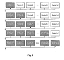
- the NAND flash devices can be arranged in the recording apparatus as a matrix of memories (as depicted in Fig. 1 of WO2007/080031 A1 and in Fig. 1 of WO2006/108755A1 ) that is controlled by several buses, to each bus B of which N NAND flash devices Device0, Device1, Device2, ..., Device N -2, Device N -1 are connected, as shown in Fig. 1 of the current application for a single one of the buses.
- the first row represents a first write period for Device0
- the second row represents a second write period for Device1, and so on.
- the last row represents the last write period for Device N -1.
- the number of NAND flash devices connected to a bus is calculated with respect to the above-mentioned bus data rate and to the above-mentioned copy time, in order to meet the requirements of the application data rate.
- the writing is performed as an interleaved multiplex.
- State-of-the-art architectures e.g. the VENOM FlashPak mentioned above
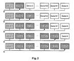
- one flash device - e.g. Device0 in Fig 2 - on bus B is not used for writing within a current write cycle.
- Fig 2 shows one write cycle starting with Device1 and ending with DeviceN.
- the first row represents a first write period for Device1, the second row represents a second write period for Device2, and so on.
- the last row represents the last write period for Device N .
- another one of the flash devices on bus B will not be used in that write cycle but Device0 is used instead in that write cycle.
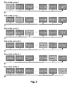
- Fig. 3 depicts a successive sequence of (completed) example bus write cycles, in each of which bus write cycles a different flash device is idle on bus B, starting with Device0 in bus write cycle 0 and ending with DeviceN in . After N+1 write cycles each flash device had been idle bus write cycle N.
- a writing error in flash memory e.g. Device0 or a newly defective writing area in that flash memory is signalled (by that flash memory)
- the information data intended for writing into a defective flash page will instead be temporally stored in a non-flash memory, e.g. an SRAM memory.
- the page information data written into a current flash memory is in parallel also written into the SRAM memory while the previously stored information data in the SRAM memory is deleted or overwritten at the appropriate time, which means that the storage capacity of the SRAM memory needs to be larger than in the other embodiment.
- three or more flash memory devices Device0, Device1,..., Device N -1 are assigned or connected to the common data bus B, and in a bus write cycle two or more of these flash memory devices are sequentially fed with the information data for storage therein.
- the information data are written into the internal cache memory section of the flash device and in a second step are transferred or programmed from that cache memory to the flash memory kernel.
- the flash memory device allows to write the information data into the cache memory section of the flash device while the previously received information data are programmed (i.e. stored) from the cache memory into the flash memory kernel (the flash memory device has two cache memory sections or two cache memories).
- the flash memory device has two cache memory sections or two cache memories.
- at least two flash memory devices Device0, Device1,..., Device N -1 are assigned or connected to the common data bus B.
Landscapes
- Engineering & Computer Science (AREA)
- Theoretical Computer Science (AREA)
- Quality & Reliability (AREA)
- Physics & Mathematics (AREA)
- General Engineering & Computer Science (AREA)
- General Physics & Mathematics (AREA)
- Techniques For Improving Reliability Of Storages (AREA)
- For Increasing The Reliability Of Semiconductor Memories (AREA)
- Debugging And Monitoring (AREA)
- Read Only Memory (AREA)
Priority Applications (8)
| Application Number | Priority Date | Filing Date | Title |
|---|---|---|---|
| EP09305611A EP2270662A1 (fr) | 2009-06-29 | 2009-06-29 | Procédé et appareil pour traiter des erreurs d'écriture lors de l'entrée de données d'information dans des dispositifs à mémoire flash |
| TW099118983A TWI503828B (zh) | 2009-06-29 | 2010-06-11 | 資訊資料書寫入快閃記憶體裝置內書寫錯誤之處理方法和裝置 |
| EP10166442.3A EP2270663B1 (fr) | 2009-06-29 | 2010-06-18 | Procédé et appareil pour traiter des erreurs d'écriture lors de l'entrée de données d'information dans des dispositifs à mémoire flash |
| US12/819,432 US8352780B2 (en) | 2009-06-29 | 2010-06-21 | Method and apparatus for dealing with write errors when writing information data into flash memory devices |
| KR1020100060107A KR101635196B1 (ko) | 2009-06-29 | 2010-06-24 | 플래시 메모리소자에 정보 데이터를 기입할 때 기입 오류를 처리하기 위한 방법 및 장치 |
| CN201010218366.8A CN101937719B (zh) | 2009-06-29 | 2010-06-28 | 将信息数据写入闪速存储器件时处理写错误的方法和装置 |
| JP2010146264A JP5575555B2 (ja) | 2009-06-29 | 2010-06-28 | 情報データをフラッシュメモリデバイスに書き込む際のライトエラーを処理する方法及び装置 |
| US13/672,122 US8468384B2 (en) | 2009-06-29 | 2012-11-08 | Method and apparatus for dealing with write errors when writing information data into memory devices |
Applications Claiming Priority (1)
| Application Number | Priority Date | Filing Date | Title |
|---|---|---|---|
| EP09305611A EP2270662A1 (fr) | 2009-06-29 | 2009-06-29 | Procédé et appareil pour traiter des erreurs d'écriture lors de l'entrée de données d'information dans des dispositifs à mémoire flash |
Publications (1)
| Publication Number | Publication Date |
|---|---|
| EP2270662A1 true EP2270662A1 (fr) | 2011-01-05 |
Family
ID=41168619
Family Applications (2)
| Application Number | Title | Priority Date | Filing Date |
|---|---|---|---|
| EP09305611A Withdrawn EP2270662A1 (fr) | 2009-06-29 | 2009-06-29 | Procédé et appareil pour traiter des erreurs d'écriture lors de l'entrée de données d'information dans des dispositifs à mémoire flash |
| EP10166442.3A Not-in-force EP2270663B1 (fr) | 2009-06-29 | 2010-06-18 | Procédé et appareil pour traiter des erreurs d'écriture lors de l'entrée de données d'information dans des dispositifs à mémoire flash |
Family Applications After (1)
| Application Number | Title | Priority Date | Filing Date |
|---|---|---|---|
| EP10166442.3A Not-in-force EP2270663B1 (fr) | 2009-06-29 | 2010-06-18 | Procédé et appareil pour traiter des erreurs d'écriture lors de l'entrée de données d'information dans des dispositifs à mémoire flash |
Country Status (6)
| Country | Link |
|---|---|
| US (2) | US8352780B2 (fr) |
| EP (2) | EP2270662A1 (fr) |
| JP (1) | JP5575555B2 (fr) |
| KR (1) | KR101635196B1 (fr) |
| CN (1) | CN101937719B (fr) |
| TW (1) | TWI503828B (fr) |
Families Citing this family (4)
| Publication number | Priority date | Publication date | Assignee | Title |
|---|---|---|---|---|
| JP2012230621A (ja) * | 2011-04-27 | 2012-11-22 | Sony Corp | メモリ装置、メモリ制御装置、メモリ制御方法 |
| JP2013058172A (ja) * | 2011-09-09 | 2013-03-28 | Toshiba Corp | 映像収録再生装置、収録方法及び再構築方法 |
| JP5800847B2 (ja) * | 2013-03-26 | 2015-10-28 | 京セラドキュメントソリューションズ株式会社 | 情報処理装置、エラー処理方法 |
| FR3077892B1 (fr) * | 2018-02-15 | 2023-12-22 | Idemia | Système et procédé d'enregistrement d'une transaction associée à une mémoire non volatile orientée page |
Citations (3)
| Publication number | Priority date | Publication date | Assignee | Title |
|---|---|---|---|---|
| WO2006108755A1 (fr) | 2005-04-15 | 2006-10-19 | Thomson Licensing | Procede et systeme pour le stockage de blocs de donnees logiques dans des blocs flash dans une pluralite de memoires non volatiles qui sont connectees a au moins un bus entree/sortie de donnees commun |
| WO2007080031A1 (fr) | 2006-01-16 | 2007-07-19 | Thomson Licensing | Procede et appareil destines a enregistrer des donnees d’entree a grande vitesse dans une matrice de dispositifs de memoire |
| US20090037652A1 (en) * | 2003-12-02 | 2009-02-05 | Super Talent Electronics Inc. | Command Queuing Smart Storage Transfer Manager for Striping Data to Raw-NAND Flash Modules |
Family Cites Families (7)
| Publication number | Priority date | Publication date | Assignee | Title |
|---|---|---|---|---|
| JPS6134793A (ja) * | 1984-07-27 | 1986-02-19 | Hitachi Ltd | ダイナミツクメモリ装置における診断及びエラ−訂正装置 |
| JP2750704B2 (ja) * | 1988-08-29 | 1998-05-13 | 日立マクセル株式会社 | Icカードの情報書込み方式及びicカード |
| JPH0433029A (ja) * | 1990-05-24 | 1992-02-04 | Matsushita Electric Ind Co Ltd | メモリ装置とその駆動方法 |
| JP4034947B2 (ja) * | 2001-05-31 | 2008-01-16 | 株式会社ルネサステクノロジ | 不揮発性記憶システム |
| JP2003006041A (ja) * | 2001-06-20 | 2003-01-10 | Hitachi Ltd | 半導体装置 |
| US8041879B2 (en) * | 2005-02-18 | 2011-10-18 | Sandisk Il Ltd | Flash memory backup system and method |
| EP1850347A1 (fr) * | 2006-04-28 | 2007-10-31 | Deutsche Thomson-Brandt Gmbh | Procédé et dispositif d'écriture pour la mémoire instantanée |
-
2009
- 2009-06-29 EP EP09305611A patent/EP2270662A1/fr not_active Withdrawn
-
2010
- 2010-06-11 TW TW099118983A patent/TWI503828B/zh not_active IP Right Cessation
- 2010-06-18 EP EP10166442.3A patent/EP2270663B1/fr not_active Not-in-force
- 2010-06-21 US US12/819,432 patent/US8352780B2/en not_active Expired - Fee Related
- 2010-06-24 KR KR1020100060107A patent/KR101635196B1/ko active IP Right Grant
- 2010-06-28 CN CN201010218366.8A patent/CN101937719B/zh not_active Expired - Fee Related
- 2010-06-28 JP JP2010146264A patent/JP5575555B2/ja not_active Expired - Fee Related
-
2012
- 2012-11-08 US US13/672,122 patent/US8468384B2/en not_active Expired - Fee Related
Patent Citations (3)
| Publication number | Priority date | Publication date | Assignee | Title |
|---|---|---|---|---|
| US20090037652A1 (en) * | 2003-12-02 | 2009-02-05 | Super Talent Electronics Inc. | Command Queuing Smart Storage Transfer Manager for Striping Data to Raw-NAND Flash Modules |
| WO2006108755A1 (fr) | 2005-04-15 | 2006-10-19 | Thomson Licensing | Procede et systeme pour le stockage de blocs de donnees logiques dans des blocs flash dans une pluralite de memoires non volatiles qui sont connectees a au moins un bus entree/sortie de donnees commun |
| WO2007080031A1 (fr) | 2006-01-16 | 2007-07-19 | Thomson Licensing | Procede et appareil destines a enregistrer des donnees d’entree a grande vitesse dans une matrice de dispositifs de memoire |
Also Published As
| Publication number | Publication date |
|---|---|
| CN101937719B (zh) | 2014-12-31 |
| EP2270663A1 (fr) | 2011-01-05 |
| EP2270663B1 (fr) | 2016-03-16 |
| TWI503828B (zh) | 2015-10-11 |
| US20100332891A1 (en) | 2010-12-30 |
| US8352780B2 (en) | 2013-01-08 |
| US20130067272A1 (en) | 2013-03-14 |
| US8468384B2 (en) | 2013-06-18 |
| KR101635196B1 (ko) | 2016-06-30 |
| JP2011008790A (ja) | 2011-01-13 |
| TW201101314A (en) | 2011-01-01 |
| CN101937719A (zh) | 2011-01-05 |
| JP5575555B2 (ja) | 2014-08-20 |
| KR20110001914A (ko) | 2011-01-06 |
Similar Documents
| Publication | Publication Date | Title |
|---|---|---|
| US8301825B2 (en) | Method and system for storing logical data blocks into flash-blocks in multiple non-volatile memories which are connected to at least one common data I/O bus | |
| US9058254B2 (en) | Memory device | |
| US8271515B2 (en) | System and method for providing copyback data integrity in a non-volatile memory system | |
| US20070214309A1 (en) | Nonvolatile storage device and data writing method thereof | |
| DE69033262T2 (de) | EEPROM-Karte mit Austauch von fehlerhaften Speicherzellen und Zwischenspeicher | |
| US8489850B2 (en) | Memory apparatus and memory control method | |
| US8041882B2 (en) | Method and device for writing to a flash memory | |
| US7802152B2 (en) | Method and apparatus for recording high-speed input data into a matrix of memory devices | |
| CN102243603B (zh) | 在编程失败之后具有可存取信息的存储器缓冲器 | |
| US20080307172A1 (en) | System and method for reproducing memory error | |
| US8468384B2 (en) | Method and apparatus for dealing with write errors when writing information data into memory devices | |
| WO2006108756A1 (fr) | Procede et systeme d'acces a des blocs de donnees logiques dans un systeme a memoires comprenant plusieurs memoires connectees a au moins un bus commun | |
| US7886211B2 (en) | Memory controller | |
| CN103389943A (zh) | 控制装置、存储装置及存储控制方法 | |
| US7996598B2 (en) | Memory management module |
Legal Events
| Date | Code | Title | Description |
|---|---|---|---|
| PUAI | Public reference made under article 153(3) epc to a published international application that has entered the european phase |
Free format text: ORIGINAL CODE: 0009012 |
|
| AK | Designated contracting states |
Kind code of ref document: A1 Designated state(s): AT BE BG CH CY CZ DE DK EE ES FI FR GB GR HR HU IE IS IT LI LT LU LV MC MK MT NL NO PL PT RO SE SI SK TR |
|
| AX | Request for extension of the european patent |
Extension state: AL BA RS |
|
| STAA | Information on the status of an ep patent application or granted ep patent |
Free format text: STATUS: THE APPLICATION IS DEEMED TO BE WITHDRAWN |
|
| 18D | Application deemed to be withdrawn |
Effective date: 20110706 |