EP2267800A2 - Puce semi-conductrice pour l'optoélectronique et son procédé de fabrication - Google Patents
Puce semi-conductrice pour l'optoélectronique et son procédé de fabrication Download PDFInfo
- Publication number
- EP2267800A2 EP2267800A2 EP10183569A EP10183569A EP2267800A2 EP 2267800 A2 EP2267800 A2 EP 2267800A2 EP 10183569 A EP10183569 A EP 10183569A EP 10183569 A EP10183569 A EP 10183569A EP 2267800 A2 EP2267800 A2 EP 2267800A2
- Authority
- EP
- European Patent Office
- Prior art keywords
- layer
- semiconductor chip
- film layer
- chip according
- carrier substrate
- Prior art date
- Legal status (The legal status is an assumption and is not a legal conclusion. Google has not performed a legal analysis and makes no representation as to the accuracy of the status listed.)
- Granted
Links
- 239000004065 semiconductor Substances 0.000 title claims description 133
- 230000005693 optoelectronics Effects 0.000 title claims description 6
- 238000004519 manufacturing process Methods 0.000 title description 9
- 239000010410 layer Substances 0.000 claims description 280
- 239000010409 thin film Substances 0.000 claims description 110
- 239000000758 substrate Substances 0.000 claims description 82
- 241000152158 Mesene Species 0.000 claims description 32
- 238000000034 method Methods 0.000 claims description 24
- 230000003287 optical effect Effects 0.000 claims description 12
- 238000005496 tempering Methods 0.000 claims description 11
- 238000001465 metallisation Methods 0.000 claims description 9
- 238000000605 extraction Methods 0.000 claims description 7
- 238000000926 separation method Methods 0.000 claims description 7
- 239000002131 composite material Substances 0.000 claims description 5
- AMGQUBHHOARCQH-UHFFFAOYSA-N indium;oxotin Chemical compound [In].[Sn]=O AMGQUBHHOARCQH-UHFFFAOYSA-N 0.000 claims description 5
- 229910052581 Si3N4 Inorganic materials 0.000 claims description 3
- HQVNEWCFYHHQES-UHFFFAOYSA-N silicon nitride Chemical compound N12[Si]34N5[Si]62N3[Si]51N64 HQVNEWCFYHHQES-UHFFFAOYSA-N 0.000 claims description 3
- 238000004026 adhesive bonding Methods 0.000 claims description 2
- 239000011247 coating layer Substances 0.000 claims description 2
- 238000005476 soldering Methods 0.000 claims description 2
- 230000007423 decrease Effects 0.000 abstract description 4
- 238000002310 reflectometry Methods 0.000 description 25
- 238000010586 diagram Methods 0.000 description 16
- 238000011835 investigation Methods 0.000 description 11
- 239000000463 material Substances 0.000 description 9
- 230000008878 coupling Effects 0.000 description 8
- 238000010168 coupling process Methods 0.000 description 8
- 238000005859 coupling reaction Methods 0.000 description 8
- 230000000694 effects Effects 0.000 description 7
- 230000008901 benefit Effects 0.000 description 6
- 230000005855 radiation Effects 0.000 description 5
- 230000008569 process Effects 0.000 description 4
- 238000005520 cutting process Methods 0.000 description 3
- 238000009792 diffusion process Methods 0.000 description 3
- 238000005530 etching Methods 0.000 description 3
- 239000010931 gold Substances 0.000 description 3
- 229910052751 metal Inorganic materials 0.000 description 3
- 239000002184 metal Substances 0.000 description 3
- 239000000203 mixture Substances 0.000 description 3
- 239000011347 resin Substances 0.000 description 3
- 229920005989 resin Polymers 0.000 description 3
- 229910001218 Gallium arsenide Inorganic materials 0.000 description 2
- 238000010521 absorption reaction Methods 0.000 description 2
- 229910052782 aluminium Inorganic materials 0.000 description 2
- 230000004888 barrier function Effects 0.000 description 2
- 230000005496 eutectics Effects 0.000 description 2
- 229910052737 gold Inorganic materials 0.000 description 2
- 230000006872 improvement Effects 0.000 description 2
- 238000005304 joining Methods 0.000 description 2
- 230000000737 periodic effect Effects 0.000 description 2
- 238000004064 recycling Methods 0.000 description 2
- 229910052709 silver Inorganic materials 0.000 description 2
- 230000035882 stress Effects 0.000 description 2
- 238000003631 wet chemical etching Methods 0.000 description 2
- 238000001039 wet etching Methods 0.000 description 2
- 229910017401 Au—Ge Inorganic materials 0.000 description 1
- 229910000530 Gallium indium arsenide Inorganic materials 0.000 description 1
- 241001295925 Gegenes Species 0.000 description 1
- VYPSYNLAJGMNEJ-UHFFFAOYSA-N Silicium dioxide Chemical compound O=[Si]=O VYPSYNLAJGMNEJ-UHFFFAOYSA-N 0.000 description 1
- 239000000853 adhesive Substances 0.000 description 1
- 230000001070 adhesive effect Effects 0.000 description 1
- 230000032683 aging Effects 0.000 description 1
- 229910045601 alloy Inorganic materials 0.000 description 1
- 239000000956 alloy Substances 0.000 description 1
- 238000005275 alloying Methods 0.000 description 1
- 238000013459 approach Methods 0.000 description 1
- 230000015572 biosynthetic process Effects 0.000 description 1
- 238000007664 blowing Methods 0.000 description 1
- 238000005266 casting Methods 0.000 description 1
- 239000002800 charge carrier Substances 0.000 description 1
- 238000003486 chemical etching Methods 0.000 description 1
- 238000005253 cladding Methods 0.000 description 1
- 230000001419 dependent effect Effects 0.000 description 1
- 238000000151 deposition Methods 0.000 description 1
- 238000010292 electrical insulation Methods 0.000 description 1
- 230000002349 favourable effect Effects 0.000 description 1
- PCHJSUWPFVWCPO-UHFFFAOYSA-N gold Chemical compound [Au] PCHJSUWPFVWCPO-UHFFFAOYSA-N 0.000 description 1
- 238000000227 grinding Methods 0.000 description 1
- 238000005259 measurement Methods 0.000 description 1
- 230000001404 mediated effect Effects 0.000 description 1
- 150000002739 metals Chemical class 0.000 description 1
- 238000002161 passivation Methods 0.000 description 1
- 230000008092 positive effect Effects 0.000 description 1
- 238000003825 pressing Methods 0.000 description 1
- 238000012545 processing Methods 0.000 description 1
- 230000006798 recombination Effects 0.000 description 1
- 238000005215 recombination Methods 0.000 description 1
- 229910052814 silicon oxide Inorganic materials 0.000 description 1
- 229910000679 solder Inorganic materials 0.000 description 1
- 238000003892 spreading Methods 0.000 description 1
- 230000007480 spreading Effects 0.000 description 1
- 230000006641 stabilisation Effects 0.000 description 1
- 238000011105 stabilization Methods 0.000 description 1
Images


Classifications
-
- H—ELECTRICITY
- H01—ELECTRIC ELEMENTS
- H01L—SEMICONDUCTOR DEVICES NOT COVERED BY CLASS H10
- H01L33/00—Semiconductor devices having potential barriers specially adapted for light emission; Processes or apparatus specially adapted for the manufacture or treatment thereof or of parts thereof; Details thereof
- H01L33/02—Semiconductor devices having potential barriers specially adapted for light emission; Processes or apparatus specially adapted for the manufacture or treatment thereof or of parts thereof; Details thereof characterised by the semiconductor bodies
- H01L33/20—Semiconductor devices having potential barriers specially adapted for light emission; Processes or apparatus specially adapted for the manufacture or treatment thereof or of parts thereof; Details thereof characterised by the semiconductor bodies with a particular shape, e.g. curved or truncated substrate
-
- H—ELECTRICITY
- H01—ELECTRIC ELEMENTS
- H01L—SEMICONDUCTOR DEVICES NOT COVERED BY CLASS H10
- H01L33/00—Semiconductor devices having potential barriers specially adapted for light emission; Processes or apparatus specially adapted for the manufacture or treatment thereof or of parts thereof; Details thereof
- H01L33/005—Processes
- H01L33/0093—Wafer bonding; Removal of the growth substrate
-
- H—ELECTRICITY
- H01—ELECTRIC ELEMENTS
- H01L—SEMICONDUCTOR DEVICES NOT COVERED BY CLASS H10
- H01L33/00—Semiconductor devices having potential barriers specially adapted for light emission; Processes or apparatus specially adapted for the manufacture or treatment thereof or of parts thereof; Details thereof
- H01L33/02—Semiconductor devices having potential barriers specially adapted for light emission; Processes or apparatus specially adapted for the manufacture or treatment thereof or of parts thereof; Details thereof characterised by the semiconductor bodies
- H01L33/08—Semiconductor devices having potential barriers specially adapted for light emission; Processes or apparatus specially adapted for the manufacture or treatment thereof or of parts thereof; Details thereof characterised by the semiconductor bodies with a plurality of light emitting regions, e.g. laterally discontinuous light emitting layer or photoluminescent region integrated within the semiconductor body
-
- H—ELECTRICITY
- H01—ELECTRIC ELEMENTS
- H01L—SEMICONDUCTOR DEVICES NOT COVERED BY CLASS H10
- H01L33/00—Semiconductor devices having potential barriers specially adapted for light emission; Processes or apparatus specially adapted for the manufacture or treatment thereof or of parts thereof; Details thereof
- H01L33/02—Semiconductor devices having potential barriers specially adapted for light emission; Processes or apparatus specially adapted for the manufacture or treatment thereof or of parts thereof; Details thereof characterised by the semiconductor bodies
- H01L33/10—Semiconductor devices having potential barriers specially adapted for light emission; Processes or apparatus specially adapted for the manufacture or treatment thereof or of parts thereof; Details thereof characterised by the semiconductor bodies with a light reflecting structure, e.g. semiconductor Bragg reflector
-
- H—ELECTRICITY
- H01—ELECTRIC ELEMENTS
- H01L—SEMICONDUCTOR DEVICES NOT COVERED BY CLASS H10
- H01L2924/00—Indexing scheme for arrangements or methods for connecting or disconnecting semiconductor or solid-state bodies as covered by H01L24/00
- H01L2924/0001—Technical content checked by a classifier
- H01L2924/0002—Not covered by any one of groups H01L24/00, H01L24/00 and H01L2224/00
-
- H—ELECTRICITY
- H01—ELECTRIC ELEMENTS
- H01L—SEMICONDUCTOR DEVICES NOT COVERED BY CLASS H10
- H01L33/00—Semiconductor devices having potential barriers specially adapted for light emission; Processes or apparatus specially adapted for the manufacture or treatment thereof or of parts thereof; Details thereof
- H01L33/02—Semiconductor devices having potential barriers specially adapted for light emission; Processes or apparatus specially adapted for the manufacture or treatment thereof or of parts thereof; Details thereof characterised by the semiconductor bodies
- H01L33/26—Materials of the light emitting region
- H01L33/30—Materials of the light emitting region containing only elements of Group III and Group V of the Periodic Table
-
- H—ELECTRICITY
- H01—ELECTRIC ELEMENTS
- H01L—SEMICONDUCTOR DEVICES NOT COVERED BY CLASS H10
- H01L33/00—Semiconductor devices having potential barriers specially adapted for light emission; Processes or apparatus specially adapted for the manufacture or treatment thereof or of parts thereof; Details thereof
- H01L33/36—Semiconductor devices having potential barriers specially adapted for light emission; Processes or apparatus specially adapted for the manufacture or treatment thereof or of parts thereof; Details thereof characterised by the electrodes
- H01L33/40—Materials therefor
- H01L33/405—Reflective materials
Definitions
- the carrier substrate is part of the semiconductor chip per se and mechanical support for the thin film layer, i. H. the essential supporting element for the thin-film layer, which no longer has a self-supporting layer even on the side opposite the carrier substrate.
- a thin-film layer based on In 1-xy Al x Ga y P means that the thin-film layer has a plurality of layers made of doped or Undoped material from the system In 1-xy Al x Ga y P (where 0 ⁇ x ⁇ 1, 0 ⁇ y ⁇ 1 and x + y ⁇ 1) are made.
- Semiconductor chips of the type mentioned are from the US 5,008,718 and US 5,367,580 known.
- an active semiconductor layer sequence is usually applied to a substrate by an epitaxial process.
- a carrier substrate is attached to the upper side of the active semiconductor layer sequence.
- the substrate on which the semiconductor layer sequence has been removed is at least partially removed.
- a metallic reflection layer is located between the carrier substrate and the active semiconductor layer sequence so that no light is absorbed by the carrier substrate.
- the metallic reflection layer arranged between the carrier substrate and the active semiconductor layer sequence generally has no satisfactory reflectivity at short wavelengths.
- gold becomes increasingly inefficient as a metallic reflection layer, since the reflectivity decreases significantly.
- the elements Al and Ag can be used whose reflectivity remains relatively constant at wavelengths less than 600 nm.
- a truncated pyramidal semiconductor chip which has an active, light-emitting zone between an upper window layer and a lower window layer.
- the upper window layer and the lower window layer together form a truncated pyramid-shaped base body.
- the oblique orientation of the side walls of the window layers causes the light emanating from the active zone to be totally reflected on the side surfaces and impinges on the base surface of the truncated pyramidal basic body serving as a luminous surface at approximately right angles. This will cause part of the active zone emitted light within the outlet cone of the semiconductor element on the surface.
- exit cone is here and shall be understood in the following the cone, which is formed of light rays whose angle of incidence on the exit surface is smaller than the critical angle for total reflection and therefore not totally reflected but are coupled directly from the semiconductor material.
- the opening angle of the exit cone is therefore twice as large as the critical angle of total reflection. Those light rays that run outside the exit cone, ie hit the exit surface at a larger angle than the critical angle of total reflection, are totally reflected.
- this concept requires a minimum thickness for the upper and lower window layer.
- the thickness of the upper and lower window layers is at least 50.8 ⁇ m (2 mils). Such a layer thickness is still in the range of feasible.
- the performance of the known semiconductor chip is to be increased, it is necessary to scale all dimensions. This results in layer thicknesses that can be produced epitaxially only at great expense. This known semiconductor chip is therefore scalable if at all then only with great technical effort.
- the present invention seeks to provide a producible in thin film semiconductor chip with improved light extraction and to provide a method for its production.
- the cross section of the cavity increases from outside to inside, that is, from the boundary to the support substrate toward the inside of the thin film layer, and the depth of the cavity is more than half the thickness of the thin film layer.
- the cavity or the plurality of mesences produced by the latter advantageously has the effect that the thin-film layer has contact surfaces on its connection side toward the carrier substrate, which surfaces have a small surface area relative to the overall cross-sectional area of the chip.
- This has the advantage that a comparatively large local pressure can be generated in the region of these reduced pressing surfaces - this is conducive to a secure connection of the carrier substrate and thin-film layer - and at the same time, the pressure on the thin-film layer can be kept sufficiently low to allow the Risk of damage to the thin film layer when connecting to the carrier substrate as far as possible excluded.
- the available bonding area is increased due to the cavity, which can also lead to the improvement of the connection between the carrier substrate and the thin film layer.
- the cavity is available for receiving excess adhesive or solder material, which makes their dosage advantageously less critical.
- side surfaces are advantageously provided by the cavity, at which part of the radiation emitted by the active zone is deflected so that it impinges on the exit surface of the active thin film layer facing away from the carrier substrate within the outlet cone.
- the reflection on the side surfaces of the mesenches at least partially replaces the reflection on a continuous planar reflection layer. It is advantageous if the side surfaces as deep as possible in the Protrude thin film layer, so that the largest possible proportion of the radiation emitted by the active zone, which does not directly on the exit surface and is coupled out, so (possibly even multiple) reflected, that is deflected that he meets at an angle to the exit surface which lies within the exit cone.
- the cavity is so deep that the active zone of the active thin film layer is severed therefrom.
- the reflection at the boundary surfaces of the mesenes causes most of the photons emitted by the active zone to strike the exit surface within the exit cone and leave the semiconductor chip.
- the thin-film layer is formed such that at least one trajectory of the photons emitted by the active zone leads from the respective mesa to one of the adjacent mesenes.
- photons that have not been reflected at one of the side surfaces of the original mesa may enter one of the adjacent mesenes and be reflected there at the side surfaces of the respective mesa so as to strike the exit surface within the exit cone.
- the mesen are equipped with concave side surfaces.
- the mesenes are covered with a reflective layer.
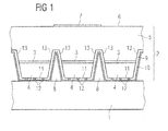
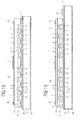
- the illustrated semiconductor chip for a light-emitting diode has a carrier substrate 1 on which the active thin-film layer 2 is mounted.
- the active thin-film layer 2 has a photon-emitting active zone 3, which is in each case formed at an average height in mesen. 4.
- the mesenes 4 may be formed like a truncated pyramid or truncated cone.
- the semiconductor chip thus constitutes a light-emitting diode.
- the mesenches 4 are arranged on a covering layer 5, which on a flat front side 6 has a central front-side contact point 7, which is preferably formed by a metallization layer.
- the backside mesenches 4 formed by cavities 8 are covered with a reflective layer consisting of a dielectric insulating layer 9 and a metallization layer 10 applied thereon.
- the insulating layer 9 is interrupted along a base surface 11 of the mesenes 4 by plated-through holes 12, which are formed by metallized sections.
- the insulating layer 9 preferably has a smaller refractive index than the adjacent semiconductor layer of the thin film layer 2. It is further formed as a diffusion barrier for the metallization layer 10. Instead of the insulating layer 9, an electrically conductive layer may also be used. Decisive are the optical properties of this layer.
- the active thin film layer 2 is first epitaxially grown on a growth substrate.
- the active thin film layer 2 can be made, for example, based on InGaAlP.
- the cover layer 5 is formed on the growth substrate and then doped with a concentration above 10 18 cm -3 in order to ensure good conductivity of the cover layer 5. Because a good conductivity of the cover layer 5 is a prerequisite for the fact that on the front side 6 of the LED chip a central contact point 7 for the supply of the active zone 3 of a plurality of meseneses 4 with current suffices.
- the composition of the cover layer 5 is chosen so that it is transparent to the photons generated in the active zone. This can usually be achieved by adjusting the band gap through the composition of the material of the cover layer 5.
- the meseneses 4 are formed with suitable wet or dry chemical etching methods. Such etching methods are known and are not the subject of the application.
- the meseneses 4 are preferably formed only in the areas provided for the semiconductor chips and there again preferably only in the areas in which light extraction can take place, that is not under contact layers 7, 43 and 49 on the upper side of the thin film layer 2.
- the provided for the semiconductor chips Areas have typical lateral outer dimensions of, for example, 400 x 400 ⁇ m 2 .
- the meseneses 4 have external dimensions which lie in the region of the layer thickness of the active thin-film layer 2. The outer dimensions of the Mesen 4 are therefore in the range of 10 microns.
- the insulating layer 9 is deposited on the meseneses 4 and the vias 12 are formed. Thereafter, the metallization layer 10 is applied.
- the active thin film layer 2 is separated according to the intended number of semiconductor chips. This is done for example by wet etching.
- the separated active thin film layers 2 are fixed to the support substrate 1 by, for example, eutectic bonding, and the growth substrate is removed by wet etching. Finally, the contact points 7 are formed on the exposed front side of the active thin-film layer 2 and the semiconductor chips are separated by separating the carrier substrate 1.
- the illustrated semiconductor chip has the advantage that the photons generated by the active zone 3 do not strike components of the semiconductor chip which absorb them. Because through the metallization 10, the Keep photons away from the carrier substrate 1.
- the carrier substrate can therefore advantageously be optimized very well with regard to electrical and / or thermal conductivity and / or thermal expansion.
- Another advantage is that when the semiconductor chip out FIG. 1 a large part of the photons emitted by the active zone 3 is totally reflected on lateral surfaces 13 of the mesenesals 4. The total reflected on the side surfaces 13 photons strike the front 6 at a large angle. In particular, a portion of the photons, which would be totally reflected without reflection on the side surfaces 13 on the front side, hits the front side 6 within the exit cone and can therefore leave the semiconductor chip. In the semiconductor chip according to FIG. 1 Therefore, the reflection on the known from the prior art continuous base surface is at least partially replaced by the total reflection at the side surfaces 13. Therefore, the semiconductor chip is turned off FIG. 1 Compared to conventional semiconductor chips without cavities 8 a nearly by a factor of 2 increased light output.
- light rays should not be understood as a limitation to a particular wavelength, but as a reference to the methods of geometric optics, regardless of the wavelength.
- the meseneses 4 are designed in the shape of a truncated pyramid and are fastened to the base substrate 11 of the mesenes via a contact layer 14 on the carrier substrate 1. Through the contact layer 14, the active zone 3 is supplied with power.
- the light beams emanating from the active zone 3 are directed in the direction of the front side 6.
- the mesenes 4 cause the light rays incident on the side surfaces 13 to be deflected in the direction of the front side 6 and impinge there within the exit cone, so that they can leave the semiconductor chip.
- the light output can be optimized by a suitable choice of the dimensions of the base 11, the angle of inclination of the side surface 13 and the height of the mesen as well as the position of the active zone 3.
- a light beam 15 is shown, which is first totally reflected on the side surface 13 and directed from there to the front 6.
- the light beam 15 strikes the interface within the exit cone and can therefore leave the semiconductor chip. Without the total reflection on the side surface 13, the light beam 15 would have been totally reflected at the front side 6 and would have been redirected to one of the reflection layers known from the prior art, where it would have been reflected again.
- the reflection on the conventional continuous reflection layer replaced by the reflection on the side surfaces 13.
- the light beam 16 is directed to the front 6 after the second reflection, where it impinges within the exit cone. Without the reflection on the side surface 13, the light beam 16 would also have been totally reflected on the front side 6 and deflected back to a rear reflection layer.
- optical coupling is to be understood as meaning that at least one of the light beams emanating from the active thin-film layer 2 can pass over a center line 17 from the region of one of the mesenes 4 into the region of one of the adjacent mesenes. Because of the optical coupling with the aid of the cover layer 5, a light beam 18, which does not strike one of the side surfaces 13 of the respective mesenes 4, meet one of the side surfaces 13 of one of the adjacent mesenes 4 and be directed there to the front 6, where it is inside of the exit cone impinges. Due to the optical coupling via the cover layer 5, therefore, the light output is further increased.
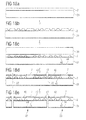
- FIG. 3 a cross section through a modified embodiment of the semiconductor chip is shown, in which the mesenes 4 are frusto-conical with concave side surfaces 13 are formed.
- the configuration of the side surfaces 13 results in a light beam 18 reflected back and forth between the front side 6 and the side surface 13 being increasingly deflected toward the front side as it approaches the center line 17 until it strikes the front side 6 within the exit cone.
- the same applies to light rays 19 which first pass over the cover layer 5 from one mesa 4 to the adjacent mesa 4 and are brought there at a large angle to the front side 6.
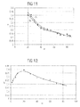
- FIG. 4 Finally, a diagram is shown in which a measurement curve 20 represents the dependence of the luminous efficiency in relative units of the operating current in pulsed operation for a conventional, manufactured in thin film light emitting diode.
- a further measuring curve 21 illustrates the dependence of the luminous efficacy in relative units as a function of the operating current for a light-emitting diode according to the in FIG FIG. 3 illustrated embodiment.
- FIG. 4 It can be seen that the light output at the in FIG. 3 illustrated embodiments, approximately twice the luminous efficacy of conventional semiconductor chips without cavities 8 has.
- FIG. 5 a cross-sectional profile of one of the meseneses 4 is shown.
- the mesa 4 is composed of a lower truncated cone 22 and an upper truncated cone 23.
- the lower truncated cone 22 adjoins the cover layer 5 with a base surface 24.
- the active zone 3 is formed in the upper truncated cone 23, the active zone 3 is formed. It is also in FIG. 5 a arranged on the base 11 of the mesa 3 contact point 25 is provided.
- the side surfaces 13 of the mesa 4 are composed of an edge 26 of the lower truncated cone 22 and flanks 27 of the upper truncated cone 23 together.
- the geometric dimensions of the lower truncated cone 22 along a common boundary surface 28 are selected so that the flank 26 merges directly into the flank 27.
- the radius of the base surface 24 of the lower truncated cone 22 is denoted by r n , the radius of the interface 28 with r t and the radius of the base 11 with r p .
- the mesa 4 may be divided into a lower confinement layer 29 between the base surface 24 and the active zone 3 and an upper confinement layer 30 between the active zone 3 and the base 11.
- the lower boundary layer 29 has a height h u and the upper boundary layer 30 has a height h o .
- the entire height of the mesa 4 is finally denoted by H. It was set consistently in all investigations equal to 6 microns. For the thickness h w of the covering layer 5, a value of 2 ⁇ m was chosen in all investigations in which the thickness h w was not varied.
- FIGS. 6a to 6d the result of a calculation is shown in which the radius r p of the base area 11 was set equal to 5 ⁇ m and the radius r n of the base area 24 equal to 20 ⁇ m.
- the radius r t of the interface 28 was between 6 and 18 ⁇ m, corresponding to those in FIG FIG. 6a to FIG. 6c varies cross-sectional profiles varies.
- a refractive index of 3.2 was used for the active zone 3.
- the refractive index of the lower confinement layer 29, the upper confinement layer 30 and the cover layer 5 was equal to 3.3.
- the reflectivity of pad 25 was 0.3.
- the reflectivity of the base area 11 not covered by the contact point 25 and of the flanks 26 and 27 was set to the value 0.8. By reflectivity is meant in each case the energy-related reflection coefficient.
- the self-absorption of the active zone 3 by an absorption coefficient of 10,000 / cm was considered. All investigations were carried out with photon recycling. For this an internal quantum efficiency of 0.8 was assumed. The quantum efficiency in the generation of photons by charge carrier recombination was not considered.
- the decoupling efficiency ⁇ indicated in the diagrams is therefore equal to the ratio of the photons decoupled from the semiconductor chip to the number of photons actually generated. The values for the specified decoupling efficiency ⁇ would therefore have to be multiplied by a factor of 0.8 in order to arrive at the external efficiency.
- FIG. 6c shows a diagram in which the decoupling efficiency ⁇ is plotted against the radius r t in a curve 31.
- the coupling-out efficiency of a normal thin-film semiconductor chip is shown, in which the scattering is mediated only by the photon recycling.
- This thin-film semiconductor chip with the edge length 300 ⁇ m has the same epitaxial structure as the mesa 4 in the lower truncated cone 22 and upper truncated cone 23. It was assumed that the semiconductor chip is provided on the p-side with a mirror whose reflectivity is 0.72.
- This value is the average value of the reflectivity of a reflection layer and a contact layer weighted with the degree of occupation, the value 0.8 being used for the reflectivity of the reflection layer and 0.85 for the occupation level of the reflection layer and the value 0 for the reflectivity of the contact layer. 3 and the occupancy rate 0.15 was used.
- FIG. 6 can be seen that at a very large angle ⁇ o of the upper truncated cone 23 according to the in FIG. 6a Cross-sectional profile shown the coupling-out efficiency ⁇ is hardly better than the coupling-out efficiency ⁇ of a conventional thin-film light emitting diode whose coupling-out efficiency in FIG. 6d is shown by the straight line 32.
- the Mesa 4 with the in FIG. 6a shown flat surface cross-sectional profile hardly brings out the emanating from the active zone 3 light rays in a steep angle to the luminous surface 6. But this is exactly what the Mesa 4 does with the in FIG. 6c shown cross-sectional profile, which is why the coupling-out efficiency ⁇ is almost twice the coupling-out efficiency ⁇ of a conventional thin-film light emitting diode in this case.
- the coupling-out efficiency ⁇ was calculated as a function of the reflectivity of the contact point 25, the cross-sectional profile of the mesa 4 being equal to that in FIG. 6b was shown cross-sectional profile.
- the contact point 25 covers the entire base area 11.
- FIG. 7 It can be seen that the coupling-out efficiency ⁇ does not depend essentially on the reflectivity of the contact point 25.
- the semiconductor chips with mesen 4 on the mounting side described here therefore appear to be much less sensitive to the poor reflectivity of the contact points 25 than the conventional thin-film light-emitting diodes, since the multiple reflections leading to the coupling appear to be only a small fraction between the base 11 and the luminous surface 6 , but three-dimensionally done in the mesa 4.
- the relative independence of the reflectivity of the pad 25 is particularly advantageous since in practice a low ohmic resistance between the pad 25 and the upper cladding layer 30 is generally associated with poor reflectivity. Because a good ohmic contact requires the diffusion of atoms from the layer forming the contact point 25 in the underlying material.
- the Mesen 4 therefore have approximately the in FIG. 6b shown cross-sectional profile.
- FIG. 8 Plotted point 34 represents the result of an invoice for a semiconductor chip to which no mirror layer has been applied, but which has been embedded in resin as the surrounding medium. However, total reflection takes place here, so that a greater outcoupling efficiency results compared to a semiconductor chip with a mirror layer. This would also be the case in FIG. 1 illustrated embodiment of the case in which between the metallization layer 10, the electrical insulating layer is arranged on the same total reflection can take place.
- the Mesen 4 therefore essentially have the FIG. 6b illustrated cross-sectional profile on.
- the active zone 3 was located at a medium height between the base surface 24 and the base surface 11.
- the area in which 3 photons are formed in the active zone was narrowed to a spot whose diameter d L is plotted on the abscissa.
- the coupling-out efficiency is particularly high for a small spot. This means that photons in the center of the active zone 3 are coupled out particularly well. In this respect, a slight Weierstrass effect is present.
- FIGS. 10a to 10c are shown various cross-sectional profiles in which the thickness h u of the lower boundary layer 29 and the thickness h u of the upper boundary layer 30 were varied so that the total height H of the mesa remained constant.
- the result of the bill is in FIG. 10d represented in which the decoupling efficiency ⁇ is plotted as a function of the thickness h u of the lower boundary layer 29. It can be seen that the coupling-out efficiency ⁇ is only slightly dependent on the position of the active zone 3.
- An active zone 3 located in the lower half of the mesa 4 is preferable because then the current density through the active zone 3 is low and therefore the current load of the active zone 3 is kept small, avoiding aging and linearity problems.
- flank angle ⁇ there is also an optimum range. This is based on FIG. 12 clear.
- the radius r p was set equal to 10 ⁇ m.
- the radius r a of the active zone 3 and the radius r n of the base surface 24 were varied so that the angle of attack ⁇ of the flanks 27 and 26 covers a range of values between 1.5 ° and 85 °. How out FIG. 12 is recognizable, there is an optimum angle range for the angle of attack ⁇ .
- the flank angle ⁇ should be between 5 ° and 60 °, preferably between 10 ° and 40 °. Particularly good values for the coupling-out efficiency ⁇ arise when the angle of attack ⁇ is between 15 ° and 30 °.
- a curve 37 in FIG. 13 illustrates the case that the reflectivity R K of the pad 25 is 0.3.
- Another curve 38 relates to the case where the reflectivity R K of the pad 25 is 0.8.
- Both the curve 37 and the curve 38 show the dependence of the coupling-out efficiency ⁇ on the diameter 2r a of the active zone 3. With good reflectivity of the contact point 25, the coupling-out efficiency ⁇ decreases only slightly with increasing diameter of the active zone 3.
- the curve 37 which realistic case shows a poor reflectivity R K of the contact point 25, however, shows that the coupling-out efficiency ⁇ decreases sharply with increasing diameter of the active zone 3.
- the coupling-out efficiency ⁇ is therefore the better the smaller the lateral extent of the meseneses 4.
- the thickness of the cover layer 5 is also important for the coupling-out efficiency ⁇ .
- the decoupling efficiency ⁇ is plotted for different cases as a function of the thickness h w of the cover layer 5.
- a curve 39 represents the already mentioned periodic case.
- a further curve 40 relates to the aperiodic case and a third curve 41 to a case in which square semiconductor chips having an edge length of 300 ⁇ m are interconnected by a connecting layer.
- the cover layer 5 is increasingly advantageous as the layer thickness increases.
- the layer thickness h w is smaller than the height of the mesenes 4, which in the present case is 6 ⁇ m. It follows that the depth of the cavities 8 should be greater than half the thickness of the active thin film layer 2.
- FIG. 15 shows a preferred embodiment of a thin-film LED chip according to the invention in a schematic representation.
- the thin-film layer 2 consists of a highly doped n-InGaAIP layer 2a (concentration> 10 17 cm -3 , preferably> 10 18 cm -3 ) with a layer thickness of about 4 ⁇ m and a Mg-doped p-GaP layer 2b with a layer thickness of about 3.5 microns.
- an insulating layer 9, for example, Si 3 N 4 and a metallic reflector contact layer 10 is applied on the attachment side 11 of the thin-film layer 2 facing the carrier substrate 1, as in connection with FIG Fig. 1 described.
- the Si 3 N 4 - layer which has a thickness of preferably about three wavelengths of the emitted radiation based on the wavelength of the light emitted by the active zone, leads in addition to their electrical insulation effect to an improved mirror effect of the metallic reflector and provides when using a suitable material simultaneously a diffusion barrier between the thin film layer 2 and metallic reflector layer 10 is.
- the insulating layer 9 may alternatively be a layer stack of, for example, alternating silicon nitride layers and silicon oxide layers.
- the p-side power supply to the active zone 3 is ensured by an alloyed AuZn contacts 12 which are arranged on the carrier substrate 1 facing surface of the mesenes 4 and passed through the insulating layer 9.
- the reflector contact layer 10 is preferably an AuZn / TiW (N) / Au layer. But it can also be made entirely of Au, Al or Ag or an alloy of these metals.
- the thin-film layer 2 is applied by bonding to the conductive carrier substrate 1, in the exemplary embodiment an n-GaAs substrate.
- Top and bottom of the carrier substrate 1 are provided, for example, with AuGe contact layers 44, 45.
- a TiPtAu / AuSn layer 47 is additionally present on the AuGe contact layer 45, for example.
- a center contact 7 and a metal frame 43 or other electrically conductive frame is provided, which is connected via two electrically conductive webs, not shown, with the center contact 7.
- the center contact 7 and the metal frame 43 are made of, for example, a TiPtAu layer and a TiAuGe layer interposed therebetween and the thin film layer 2.
- the high conductivity of the n-InGaAIP layer ensures the required current spreading.
- an optical tempering layer 42 is arranged on the front side of the thin film layer 2, in the exemplary embodiment a ⁇ / 4 layer of Si 3 N 4 .
- a plurality of pyramidal truncated cavities 8 are formed, which significantly increase the light extraction of the light emitting diode.
- the cavities 8 extend so far into the thin-film layer 2 that they interrupt the pn junction 3.
- the cavities 8 can also be designed so deep that they do not sever the pn junction.
- the cavities 8 additionally have the advantage that they significantly reduce the stresses occurring during eutectic bonding of the thin-film layer 2 to the carrier substrate 1 due to the different thermal expansion coefficients of the various materials. Thus, process reliability and manufacturing yield are increased.
- FIG. 16 shows a further semiconductor chip according to the invention in a schematic representation.
- the thin film layer 2 is mounted on an electrically insulating support substrate 1 so that the power supply to the p-side of the pn junction 3 via one adjacent to the thin film layer 2 arranged on the Au-Ge contact layer 45 arranged p-contact 46.
- the p-InGaAlP layer 2b has a thickness of 6 ⁇ m
- the n-InGaAlP: Te layer 2a doped with 1 ⁇ 10 18 cm -3 has a thickness of 3 ⁇ m.
- the cavities 8 in this embodiment extend to a depth of 5.5 ⁇ m. They do not interrupt the pn junction 3 in this embodiment.
- an optical tempering layer 48 made of conductive indium-tin oxide is attached by way of example in this embodiment, which also contributes to the expansion of the current in addition to the improvement of the light outcoupling. Consequently, the n-layer 2a may possibly be made thinner here than when using an electrically insulating tempering layer, because then the current widening does not have to take place exclusively in the thin-film layer 2.
- Such an electrically conductive tempering layer 48 may also be used in all other embodiments of the semiconductor chip according to the invention.
- an insulating tempering layer 42 may be used instead of the indium tin oxide layer 48.
- the structure shown is also suitable when using a conductive carrier substrate 1 and is not limited to the use of an electrically insulating carrier substrate 1.
- the structure of the embodiment of FIG. 16 has the advantage that the carrier substrate 1 can advantageously be optimized in particular with regard to thermal expansion and / or thermal conductivity, without having to pay attention to its electrical conductivity.
- the cavities 8 can be filled with a suitable material for processing the thin-film layer.
- FIGS. 17a to 17e illustrated method sequence for simultaneously producing a plurality of semiconductor chips according to the invention shows schematic representations of vertical sections through a wafer at different times of the manufacturing process.
- the active thin film layer 2 as well as the layers explained above between the carrier substrate and the thin film layer with all its details has been described here and also in the descriptions of the methods of the FIGS. 18a to 19e omitted for simplicity.
- the thin-film layer 2, the insulating layer 9, the contact layers 7, 43-47 and 49 and the tempering layer 42, 48 are produced, for example, by conventional deposition methods known in the semiconductor art.
- an active thin-film layer 2 is grown on a growth substrate 20 ( Figure 17a ).
- a thin film layer 2 typically comprises a plurality of semiconductor layers of different compositions.
- the cavities 8 are formed. This is done for example by a suitable mask technique and anisotropic wet chemical etching ( FIG. 17b ).
- the reflective layer 9,10 (not shown here, but see for example the FIGS. 15 and 16 ) are applied and are the mesenches 4, the vias 12 (not shown here, but see for example the FIGS. 15 and 16 ) before this side is subsequently connected to a carrier substrate wafer 21, on the main surfaces of which there are preferably contact layers 44, 45 ( FIG. 17c ).
- a bonding pad 7 is applied to the exposed surface of the thin-film layer 2 in each surface area in which a semiconductor chip is to be formed, by means of connecting webs 49 (see FIG FIG. 20 ) a power supply frame 43 is connected, which runs at the outer edge of the thin film layer 2 of the later chip. Exemplary materials of such contact layers are already mentioned above.
- the radiation decoupling surfaces of the later chips, which are located between the bonding pads 7 and the contacting frame 70, are provided with an optical coating layer 42. Compare to this FIG. 17d ,
- the thin-film layer 2 is preferably severed along the separation paths 22 by means of etching and, if necessary, a damage etching is carried out on the resulting flanks of the thin-film layer.
- the flanks of the thin film layer 2 may, if necessary, be provided with a tempering layer and / or passivation layer.
- the carrier substrate wafer 21 is then severed, for example by means of sawing or scribing and breaking along the separation paths 22, so that individual semiconductor chips 23 are formed.
- the complete production of the semiconductor chips is thus advantageously carried out in the laminated pane; that is, the separation of the wafer into individual chips is the last Step of the process is before, for example, the chips are mounted in enclosures at a later date.
- FIGS. 18a to 18e The method illustrated differs from that of FIGS. 17a-17e essentially by omitting the separate severing of the thin film layer 2 before cutting the carrier substrate wafer 21 and cutting the thin film layer 2 together with the cutting of the carrier substrate wafer 21 along the dividing lines 22 in one step.
- FIGS. 19a to 19e The method illustrated differs from that of FIGS. 17a-17e essentially in that the separate severing of the thin-film layer 2 takes place before the thin-film layer 2 is connected to the carrier substrate wafer 21.
- the removal of the growth substrate can also be done by means of blowing off instead of by means of grinding and / or wet-chemical etching.
- an absorbing layer is preferably introduced between the thin film layer and the growth substrate, which has a smaller band gap than the growth substrate.
- the absorbing layer is destroyed by means of a laser of suitable wavelength.
- the absorbing layer is InGaAs, and the laser is an IR laser, for example.
- FIG. 20 pictured view of a chip according to the invention from above, the mesenches 4 produced by means of cavities 8 are visible. It can be seen in particular that in the areas of the contact 7, the connecting webs 49, the power supply frame 43 and the separation tracks no cavities 8 are present. These are all areas in which no or only little radiation would be decoupled anyway. The omission of the cavities in these areas leads advantageously to a significant mechanical stabilization of the thin film layer 2. This has a positive effect, in particular in the region of the contact 7, because there is usually placed and pressed in the mounting of the semiconductor chip in a housing a bonding wire.
- FIG. 21 shows an oblique view of a surface of a thin-film layer 2 after the cavities 8 are formed.
- FIG. 22 shows an enlarged section of FIG. 21 .
Landscapes
- Engineering & Computer Science (AREA)
- Manufacturing & Machinery (AREA)
- Computer Hardware Design (AREA)
- Microelectronics & Electronic Packaging (AREA)
- Power Engineering (AREA)
- Led Devices (AREA)
- Led Device Packages (AREA)
Priority Applications (1)
| Application Number | Priority Date | Filing Date | Title |
|---|---|---|---|
| EP17173235.7A EP3240048B1 (fr) | 2000-08-08 | 2001-08-08 | Puce semi-conductrice pour l'optoélectronique et son procédé de fabrication |
Applications Claiming Priority (3)
| Application Number | Priority Date | Filing Date | Title |
|---|---|---|---|
| DE10038671A DE10038671A1 (de) | 2000-08-08 | 2000-08-08 | Halbleiterchip für die Optoelektronik |
| DE10059532A DE10059532A1 (de) | 2000-08-08 | 2000-11-30 | Halbleiterchip für die Optoelektronik |
| EP01984505.6A EP1307928B1 (fr) | 2000-08-08 | 2001-08-08 | Puce de semi-conducteur pour optoelectronique et son procede de fabrication |
Related Parent Applications (3)
| Application Number | Title | Priority Date | Filing Date |
|---|---|---|---|
| EP01984505.6 Division | 2001-08-08 | ||
| EP01984505.6A Division EP1307928B1 (fr) | 2000-08-08 | 2001-08-08 | Puce de semi-conducteur pour optoelectronique et son procede de fabrication |
| EP01984505.6A Division-Into EP1307928B1 (fr) | 2000-08-08 | 2001-08-08 | Puce de semi-conducteur pour optoelectronique et son procede de fabrication |
Related Child Applications (2)
| Application Number | Title | Priority Date | Filing Date |
|---|---|---|---|
| EP17173235.7A Division EP3240048B1 (fr) | 2000-08-08 | 2001-08-08 | Puce semi-conductrice pour l'optoélectronique et son procédé de fabrication |
| EP17173235.7A Division-Into EP3240048B1 (fr) | 2000-08-08 | 2001-08-08 | Puce semi-conductrice pour l'optoélectronique et son procédé de fabrication |
Publications (3)
| Publication Number | Publication Date |
|---|---|
| EP2267800A2 true EP2267800A2 (fr) | 2010-12-29 |
| EP2267800A3 EP2267800A3 (fr) | 2012-04-04 |
| EP2267800B1 EP2267800B1 (fr) | 2017-07-12 |
Family
ID=7651719
Family Applications (2)
| Application Number | Title | Priority Date | Filing Date |
|---|---|---|---|
| EP17173235.7A Expired - Lifetime EP3240048B1 (fr) | 2000-08-08 | 2001-08-08 | Puce semi-conductrice pour l'optoélectronique et son procédé de fabrication |
| EP10183569.2A Expired - Lifetime EP2267800B1 (fr) | 2000-08-08 | 2001-08-08 | Puce semi-conductrice pour l'optoélectronique et son procédé de fabrication |
Family Applications Before (1)
| Application Number | Title | Priority Date | Filing Date |
|---|---|---|---|
| EP17173235.7A Expired - Lifetime EP3240048B1 (fr) | 2000-08-08 | 2001-08-08 | Puce semi-conductrice pour l'optoélectronique et son procédé de fabrication |
Country Status (3)
| Country | Link |
|---|---|
| EP (2) | EP3240048B1 (fr) |
| CN (1) | CN100557835C (fr) |
| DE (1) | DE10038671A1 (fr) |
Families Citing this family (11)
| Publication number | Priority date | Publication date | Assignee | Title |
|---|---|---|---|---|
| DE102004021175B4 (de) | 2004-04-30 | 2023-06-29 | OSRAM Opto Semiconductors Gesellschaft mit beschränkter Haftung | Halbleiterchips für die Optoelektronik und Verfahren zu deren Herstellung |
| KR100595884B1 (ko) * | 2004-05-18 | 2006-07-03 | 엘지전자 주식회사 | 질화물 반도체 소자 제조 방법 |
| DE102007003282B4 (de) | 2007-01-23 | 2023-12-21 | OSRAM Opto Semiconductors Gesellschaft mit beschränkter Haftung | Leuchtdiodenchip |
| DE102009018603B9 (de) * | 2008-04-25 | 2021-01-14 | Samsung Electronics Co., Ltd. | Leuchtvorrichtung und Herstellungsverfahren derselben |
| KR101506264B1 (ko) * | 2008-06-13 | 2015-03-30 | 삼성전자주식회사 | 발광 소자, 발광 장치 및 상기 발광 소자의 제조 방법 |
| KR101332794B1 (ko) * | 2008-08-05 | 2013-11-25 | 삼성전자주식회사 | 발광 장치, 이를 포함하는 발광 시스템, 상기 발광 장치 및발광 시스템의 제조 방법 |
| CN102468394A (zh) * | 2010-11-12 | 2012-05-23 | 佛山市奇明光电有限公司 | 发光二极管元件及其制造方法 |
| DE102013107971A1 (de) * | 2013-07-25 | 2015-01-29 | Osram Opto Semiconductors Gmbh | Optoelektronischer Halbleiterchip, Halbleiterbauelement und Verfahren zur Herstellung von optoelektronischen Halbleiterchips |
| US9870927B2 (en) * | 2015-04-02 | 2018-01-16 | Microsoft Technology Licensing, Llc | Free-edge semiconductor chip bending |
| JP7079106B2 (ja) | 2018-01-24 | 2022-06-01 | シャープ株式会社 | 画像表示素子、及び画像表示素子の製造方法 |
| US20240153985A1 (en) * | 2021-02-01 | 2024-05-09 | Beijing Seetrum Technology Co., Ltd. | Manufacturing method for optical device, and optical device |
Citations (3)
| Publication number | Priority date | Publication date | Assignee | Title |
|---|---|---|---|---|
| US5008718A (en) | 1989-12-18 | 1991-04-16 | Fletcher Robert M | Light-emitting diode with an electrically conductive window |
| US5367580A (en) | 1990-01-29 | 1994-11-22 | Ezel, Inc. | Method and system for establishing a coincidence between two images |
| DE19807758A1 (de) | 1997-06-03 | 1998-12-10 | Hewlett Packard Co | Lichtemittierendes Element mit verbesserter Lichtextraktion durch Chipformen und Verfahren zum Herstellen desselben |
Family Cites Families (8)
| Publication number | Priority date | Publication date | Assignee | Title |
|---|---|---|---|---|
| DE1589099C3 (de) * | 1967-09-09 | 1975-08-28 | Siemens Ag, 1000 Berlin Und 8000 Muenchen | Leuchtanordnung |
| JPS5310840B2 (fr) * | 1972-05-04 | 1978-04-17 | ||
| US4039890A (en) * | 1974-08-16 | 1977-08-02 | Monsanto Company | Integrated semiconductor light-emitting display array |
| JPS52124885A (en) * | 1976-04-12 | 1977-10-20 | Matsushita Electric Ind Co Ltd | Semiconductor light emitting device |
| JPH06318731A (ja) * | 1993-03-12 | 1994-11-15 | Sharp Corp | 半導体発光装置 |
| JP2927158B2 (ja) * | 1993-09-29 | 1999-07-28 | サンケン電気株式会社 | 半導体発光素子 |
| DE59814431D1 (de) * | 1997-09-29 | 2010-03-25 | Osram Opto Semiconductors Gmbh | Halbleiterlichtquelle und Verfahren zu ihrer Herstellung |
| EP0977063A1 (fr) * | 1998-07-28 | 2000-02-02 | Interuniversitair Micro-Elektronica Centrum Vzw | Socle et système pour interconnection optoélectronique et méthode de fabrication d'un tel socle et système |
-
2000
- 2000-08-08 DE DE10038671A patent/DE10038671A1/de not_active Ceased
-
2001
- 2001-08-08 EP EP17173235.7A patent/EP3240048B1/fr not_active Expired - Lifetime
- 2001-08-08 CN CNB2007101529351A patent/CN100557835C/zh not_active Expired - Lifetime
- 2001-08-08 EP EP10183569.2A patent/EP2267800B1/fr not_active Expired - Lifetime
Patent Citations (3)
| Publication number | Priority date | Publication date | Assignee | Title |
|---|---|---|---|---|
| US5008718A (en) | 1989-12-18 | 1991-04-16 | Fletcher Robert M | Light-emitting diode with an electrically conductive window |
| US5367580A (en) | 1990-01-29 | 1994-11-22 | Ezel, Inc. | Method and system for establishing a coincidence between two images |
| DE19807758A1 (de) | 1997-06-03 | 1998-12-10 | Hewlett Packard Co | Lichtemittierendes Element mit verbesserter Lichtextraktion durch Chipformen und Verfahren zum Herstellen desselben |
Also Published As
| Publication number | Publication date |
|---|---|
| CN101132047A (zh) | 2008-02-27 |
| EP3240048A1 (fr) | 2017-11-01 |
| EP2267800A3 (fr) | 2012-04-04 |
| CN100557835C (zh) | 2009-11-04 |
| EP2267800B1 (fr) | 2017-07-12 |
| EP3240048B1 (fr) | 2021-02-17 |
| DE10038671A1 (de) | 2002-02-28 |
Similar Documents
| Publication | Publication Date | Title |
|---|---|---|
| EP1307928B1 (fr) | Puce de semi-conducteur pour optoelectronique et son procede de fabrication | |
| DE19807758B4 (de) | Lichtemittierende Diodenstruktur und Verfahren zu deren Herstellung | |
| DE69408374T2 (de) | Lichtemittierende Halbleitervorrichtung | |
| EP2149160B1 (fr) | Composant optoélectronique et procédé de fabrication d'une pluralité de composants optoélectroniques | |
| EP3200247B1 (fr) | Puce semi-conductrice et procédé de fabrication d'une puce semi-conductrice | |
| EP1592072B1 (fr) | Dispositif semiconducteur optoélectronique et son procédé de fabrication | |
| DE102005048408B4 (de) | Dünnfilm-Halbleiterkörper | |
| EP2612372B1 (fr) | Puce de diode électroluminescente | |
| DE112005003476T5 (de) | Substratentfernungsprozess für LEDs mit hoher Lichtausbeute | |
| DE102006015788A1 (de) | Optoelektronischer Halbleiterchip | |
| DE102007004302A1 (de) | Halbleiterchip und Verfahren zur Herstellung eines Halbleiterchips | |
| EP2260516A1 (fr) | Puce semiconductrice optoélectronique et procédé de fabrication associé | |
| WO1998007195A1 (fr) | Procede pour fabriquer un corps semi-conducteur emettant et/ou recevant de la lumiere | |
| EP2980864B1 (fr) | Puce semi-conductrice optoelectronique et procede de fabrication d'une puce semi-conductrice optoelectronique | |
| EP2267800B1 (fr) | Puce semi-conductrice pour l'optoélectronique et son procédé de fabrication | |
| EP1770792B1 (fr) | Puce à semi-conducteur émetteur de lumière | |
| WO2012107289A1 (fr) | Puce semiconductrice optoélectronique à couche miroir encapsulée | |
| EP2160773B1 (fr) | Puce semi-conductrice optoélectronique | |
| WO2019020424A1 (fr) | Puce semi-conductrice optoélectronique, puce semi-conductrice à haut voltage et procédé de fabrication d'une puce semi-conductrice optoélectronique | |
| WO2018010883A1 (fr) | Composant possédant une efficacité accrue et procédé de fabrication d'un composant | |
| DE10059532A1 (de) | Halbleiterchip für die Optoelektronik | |
| WO2010034279A1 (fr) | Composant optoélectronique | |
| DE10224219A1 (de) | Lichtemittierendes Halbleiterbauelement | |
| DE20019477U1 (de) | Halbleiterchip für die Optoelektronik |
Legal Events
| Date | Code | Title | Description |
|---|---|---|---|
| PUAI | Public reference made under article 153(3) epc to a published international application that has entered the european phase |
Free format text: ORIGINAL CODE: 0009012 |
|
| AC | Divisional application: reference to earlier application |
Ref document number: 1307928 Country of ref document: EP Kind code of ref document: P |
|
| AK | Designated contracting states |
Kind code of ref document: A2 Designated state(s): DE FR GB |
|
| PUAL | Search report despatched |
Free format text: ORIGINAL CODE: 0009013 |
|
| AK | Designated contracting states |
Kind code of ref document: A3 Designated state(s): DE FR GB |
|
| RIC1 | Information provided on ipc code assigned before grant |
Ipc: H01L 33/20 20100101ALI20120228BHEP Ipc: H01L 33/08 20100101ALI20120228BHEP Ipc: H01L 33/00 20100101AFI20120228BHEP Ipc: H01L 33/10 20100101ALI20120228BHEP |
|
| 17P | Request for examination filed |
Effective date: 20120808 |
|
| 17Q | First examination report despatched |
Effective date: 20130919 |
|
| GRAP | Despatch of communication of intention to grant a patent |
Free format text: ORIGINAL CODE: EPIDOSNIGR1 |
|
| INTG | Intention to grant announced |
Effective date: 20170126 |
|
| RIN1 | Information on inventor provided before grant (corrected) |
Inventor name: WEGLEITER, WALTER Inventor name: ILLEK, STEFAN Inventor name: STREUBEL, KLAUS Inventor name: PLOESSL, ANDREAS Inventor name: WIRTH, RALPH |
|
| GRAS | Grant fee paid |
Free format text: ORIGINAL CODE: EPIDOSNIGR3 |
|
| GRAA | (expected) grant |
Free format text: ORIGINAL CODE: 0009210 |
|
| AC | Divisional application: reference to earlier application |
Ref document number: 1307928 Country of ref document: EP Kind code of ref document: P |
|
| AK | Designated contracting states |
Kind code of ref document: B1 Designated state(s): DE FR GB |
|
| REG | Reference to a national code |
Ref country code: GB Ref legal event code: FG4D Free format text: NOT ENGLISH |
|
| REG | Reference to a national code |
Ref country code: FR Ref legal event code: PLFP Year of fee payment: 17 |
|
| REG | Reference to a national code |
Ref country code: DE Ref legal event code: R096 Ref document number: 50116629 Country of ref document: DE Ref country code: DE Ref legal event code: R082 Ref document number: 50116629 Country of ref document: DE Representative=s name: EPPING HERMANN FISCHER, PATENTANWALTSGESELLSCH, DE Ref country code: DE Ref legal event code: R082 Ref document number: 50116629 Country of ref document: DE Representative=s name: EPPING HERMANN FISCHER PATENTANWALTSGESELLSCHA, DE |
|
| REG | Reference to a national code |
Ref country code: DE Ref legal event code: R097 Ref document number: 50116629 Country of ref document: DE |
|
| PLBE | No opposition filed within time limit |
Free format text: ORIGINAL CODE: 0009261 |
|
| STAA | Information on the status of an ep patent application or granted ep patent |
Free format text: STATUS: NO OPPOSITION FILED WITHIN TIME LIMIT |
|
| 26N | No opposition filed |
Effective date: 20180413 |
|
| REG | Reference to a national code |
Ref country code: FR Ref legal event code: PLFP Year of fee payment: 18 |
|
| PGFP | Annual fee paid to national office [announced via postgrant information from national office to epo] |
Ref country code: GB Payment date: 20200826 Year of fee payment: 20 Ref country code: FR Payment date: 20200821 Year of fee payment: 20 Ref country code: DE Payment date: 20200819 Year of fee payment: 20 |
|
| REG | Reference to a national code |
Ref country code: DE Ref legal event code: R071 Ref document number: 50116629 Country of ref document: DE |
|
| REG | Reference to a national code |
Ref country code: GB Ref legal event code: PE20 Expiry date: 20210807 |
|
| PG25 | Lapsed in a contracting state [announced via postgrant information from national office to epo] |
Ref country code: GB Free format text: LAPSE BECAUSE OF EXPIRATION OF PROTECTION Effective date: 20210807 |