EP2264610B1 - Verbindungsnetz mit dynamischen Unternetzen - Google Patents
Verbindungsnetz mit dynamischen Unternetzen Download PDFInfo
- Publication number
- EP2264610B1 EP2264610B1 EP10164557A EP10164557A EP2264610B1 EP 2264610 B1 EP2264610 B1 EP 2264610B1 EP 10164557 A EP10164557 A EP 10164557A EP 10164557 A EP10164557 A EP 10164557A EP 2264610 B1 EP2264610 B1 EP 2264610B1
- Authority
- EP
- European Patent Office
- Prior art keywords
- circuits
- signal
- devices
- interconnection network
- network
- Prior art date
- Legal status (The legal status is an assumption and is not a legal conclusion. Google has not performed a legal analysis and makes no representation as to the accuracy of the status listed.)
- Not-in-force
Links
Images

Classifications
-
- G—PHYSICS
- G06—COMPUTING OR CALCULATING; COUNTING
- G06F—ELECTRIC DIGITAL DATA PROCESSING
- G06F13/00—Interconnection of, or transfer of information or other signals between, memories, input/output devices or central processing units
- G06F13/38—Information transfer, e.g. on bus
- G06F13/40—Bus structure
- G06F13/4004—Coupling between buses
- G06F13/4022—Coupling between buses using switching circuits, e.g. switching matrix, connection or expansion network
-
- Y—GENERAL TAGGING OF NEW TECHNOLOGICAL DEVELOPMENTS; GENERAL TAGGING OF CROSS-SECTIONAL TECHNOLOGIES SPANNING OVER SEVERAL SECTIONS OF THE IPC; TECHNICAL SUBJECTS COVERED BY FORMER USPC CROSS-REFERENCE ART COLLECTIONS [XRACs] AND DIGESTS
- Y02—TECHNOLOGIES OR APPLICATIONS FOR MITIGATION OR ADAPTATION AGAINST CLIMATE CHANGE
- Y02D—CLIMATE CHANGE MITIGATION TECHNOLOGIES IN INFORMATION AND COMMUNICATION TECHNOLOGIES [ICT], I.E. INFORMATION AND COMMUNICATION TECHNOLOGIES AIMING AT THE REDUCTION OF THEIR OWN ENERGY USE
- Y02D10/00—Energy efficient computing, e.g. low power processors, power management or thermal management
Definitions
- the invention relates to a dynamic interconnection network, that is to say a network whose topology, or connections within this network, can change depending on the sources and destinations of the data to be routed.
- the invention is particularly applicable to the interconnection of multiple processors (for example arranged in "cluster” or cluster) to multiple memory blocks, for example a shared memory by these processors.
- a dynamic interconnect network is a network whose topology, that is, connections, may vary during program execution or between different program executions. This type of interconnection network finds particular applications in the field of parallel computer architectures.
- the figure 1 schematically represents a dynamic network 1 connecting n first elements, for example five memory blocks 3.1 - 3.5 of a shared memory 3, and m second elements, for example elementary processors 5.1 - 5.6, with n and m natural numbers not zero.
- Such a dynamic network 1 allows each processor 5.1 - 5.6 to communicate with each of the memory blocks 3.1 - 3.5. So the data stored in memory blocks 3.1 - 3.5 can be shared between all 5.1 - 5.6 processors.
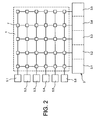
- This dynamic network 1 can be realized in the form of a "crossbar" network, as shown in FIG. figure 2 .
- This dynamic network comprises n ⁇ m switches 7, that is to say 30 switches on the example of the figure 2 , interconnected in the form of a grid 5 x 6 (6 rows, 5 columns).
- the switches 7 on a path connecting this processor and this memory block are active in order to form a communication link between this processor and this memory block.
- An object of the present invention is to propose a new interconnection network architecture making it possible to simultaneously make several parallel and independent connections of different elements to each other.
- This network of interconnections generally applies to all types of electronic, electrical, microelectronic, nanoelectronic or photonic circuits.
- Such a network offers the first m circuits the possibility of sharing information such as data stored and / or read in the n second circuits. Moreover, since this network is composed of as many subnetworks as of first circuits, each of the m subnetworks can therefore operate autonomously and simultaneously with the other subnetworks. Thus, all the first m first circuits can simultaneously communicate with the n second circuits.
- control means can therefore make some of the repetition devices active and render the other repetition devices inactive to form a communication path in the information transfer bus.
- the first m circuits may be, or include, processors, and / or the n second circuits may be, or include, memory blocks of a memory shared by the first m circuits. Each memory block may comprise several separate memory registers.
- the signal repetition devices of the information transfer bus can be bidirectional, allowing both read and write operations on the same communication bus.
- the addressing bus may comprise a plurality of portions of signal transmission lines, for example electrically conductive wires or else optical transmission lines such as optical fibers, interconnected by signal repetition devices.
- the signal repetition devices may include logic circuits.
- the control means for the repetition devices may further comprise means for selecting at least one of the n second circuits to perform at least one operation of reading and / or writing data in said one of the n second circuits, and / or access priority management means for the n second circuits by the first m circuits and / or storage means of several second circuit addresses.
- the control means may comprise a plurality of control devices, each control device being able to make active or inactive one of said repeat devices as a function of the value of the addressing signal.
- the control devices can be implemented in the shared memory.
- the control means may comprise n control devices.
- Each of the control devices may comprise similar logic circuits, a separate code being intended to be applied at the input of each control device for identifying at least one of the n second circuits.
- These codes can be stored, or hard-coded, in memory, and applied to the inputs of the controllers so that they can differentiate from each other.
- Each interconnection subnetwork may comprise a second information transfer bus comprising a plurality of signal transmission line portions interconnected by second signal repetition devices, the control means being capable of making at least one active one of the second repeater devices as a function of the value of the addressing signal, the second active repeater device forming, in the second information transfer bus, a signal communication path between said one of the first m circuits and said one of the n second circuits or between said one of the n second circuits and said second one of the n second circuits.
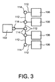
- FIG 3 schematically represents a subnetwork of interconnections connecting a first electronic circuit 102, for example here a processor, to several second electronic circuits 106, for example here four memory blocks of a shared memory.
- an interconnection network to which this subnetwork of interconnections belongs comprises one or more other subnetworks of interconnections, for example similar to the subnetwork represented on this figure 3 , and connecting other first electronic circuits 102 to the four memory blocks 106.
- the subnetwork of interconnections shown on the figure 3 allows the processor 102 to write or read data in the memory blocks 106.
- the sub-network comprises several portions of transmission lines, for example conductive tracks, forming an address bus and a transfer bus information between the processor 102 and each of the four memory blocks 106.
- the information transfer bus is represented by portions of conductive tracks 112.
- the information transfer bus is bi-directional here and makes it possible to route, for example, data signals transmitted by the processor 102 to be written in at least one of the memory blocks 106, and / or data signals which are read by the processor 102 from at least one of the memory blocks 106, and / or data signals routed from one of the memory blocks 106 to at least one other memory block 106 by the control of the processor 102.
- This information transfer bus is also configurable, that is to say that each data signal transmitted on this bus is transmitted only to the memory block 106 or to the processor 102 for which this signal is intended, by forming a specific communication path in the sub. -net for this data signal.
- the information transfer bus may be unidirectional.
- the information transfer bus furthermore makes it possible to convey information other than the data itself, for example read / write signals whose value indicates whether a read operation or a write operation in which the memory block 106, and possibly request validation signals validating or not the implementation of the read / write operation.
- the read / write signal can be used when the information transfer bus is bidirectional, to determine the direction of transition of data in this bus (processor 102 to a memory block 106 or vice versa).
- each of the memory blocks 106 comprises a plurality of memory sub-blocks each forming a different storage location, such as memory registers, to pass on the information transfer bus the address of the subsystem. destination memory block (called "Chip Select”), for example in the form of a signal separate from the signal comprising the data sent or of one or more bits concatenated to the bits of the sent data.
- Other signals can also be transmitted on the information transfer bus.
- the addressing bus makes it possible to route destination memory block addressing signals 106, whose value designates the memory block 106 in which the read or write operation is performed.
- This address bus can be unidirectional.
- the address bus is here not configurable because the signals sent on the address bus are transmitted to all the memory blocks 106 so that each memory block 106 can analyze this data and a communication path between the processor 102 and the destination memory block 106 can be established.
- the information transfer bus is configurable by means of signal repetition devices 114 arranged between each conductive track portion 112 and making it possible to connect these portions 112 to each other and thus form continuous communication paths.
- Each of these devices repetition 114 can be made active or inactive, for example by feeding it electrically or not. It is thus possible to define in each sub-network a communication path by only making active the repetition devices 114 located on the path between the processor 102 and the memory block 106 in which the processor 102 is intended to write the data. or from which the processor 102 is intended to read the data.
- the repeat devices 114 are activated or not depending on the value of the signal transmitted on the addressing bus which is read by control means, not shown on the figure 3 , these control means supplying or not electrically each of the repetition devices 114 according to whether or not the repeater 114 is on the communication path to be established in the information transfer bus.
- control means may comprise registers able to store several addresses and thus successively configure several communication paths in the information transfer bus in order to successively route several data signals to separate memory blocks 106 and / or the processor 102.
- the interconnection subnetwork here to include a second information transfer bus capable of transmitting other signals between the processor 102 and one of the memory blocks 106, parallel to the first bus of transfer of information.
- this second transfer bus of information can be configurable by the activation or not of repeaters to form a specific communication path between the processor 102 and at least one of the memory blocks 106 or between two memory blocks 106.
- This second information transfer bus can also be bidirectional or unidirectional depending on the type of information to be conveyed.
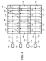
- FIG. 4 represents a network of interconnections 100 according to a particular embodiment, which allows four processors 102 to write or read data in a shared memory 104, having a plurality of memory blocks 106 (six of which are shown in FIG. figure 4 ) simultaneously and independently of each other.
- This network of interconnections 100 comprises several sub-networks, each sub-network connecting one of the processors 102 to the six memory blocks 106 by means of at least one information transfer bus and an address bus.
- Each sub-network is composed of several bundles of electrically conductive wires, or conductive portions (for example conducting tracks), forming an information transfer bus and an addressing bus between one of the processors 102 and each of the blocks. 106.
- the information transfer buses of these subnets are bi-directional and allow signals to be transmitted from one of the processors 102 to be written to the memory 104, and / or data signals that are read by one of the processors 102 from this memory 104, and / or data signals routed from one of the memory blocks 106 to one or more other memory blocks 106.
- the information transfer buses are also configurable, that is, each data signal transmitted on these buses is transmitted only to the memory block 106 or to the processor 102 for which this signal is intended.
- the addressing buses make it possible to route destination memory block addressing signals whose values denote the memory blocks 106 in which the read or write operations are performed. writing will be done.
- These addressing buses are not configurable because, unlike the signals transmitted on the information transfer buses, the addressing signals sent on the addressing buses are transmitted to all the memory blocks 106 so that each memory block can analyzing this data, that the memory block 106 concerned can be activated and that a communication path between the transmitter processor 102 and the destination memory block 106 can be established.
- each interconnection subnetwork bus comprises two vertical wire bundles 112b, each of these beams connecting the memory blocks 106 of the same column between them, and a horizontal wire bundle 112a connecting one of the processors 102 to the two vertical son bundles 112b.
- the wire bundles 112a and 112b of each bus of each subnet are segmented into several parts. Thus, the length of each wire segment is reduced, which limits the capacity formed by these segments son.
- Signal repetition devices 114 are disposed between each wire segment of each wire bundle to connect these wire segments together and form continuous communication paths. The repetition devices 114 make it possible in particular to straighten the slope of the transmitted signal and thus to carry out a transmission of amplitude signals in a sufficiently short time on all the wire bundles, between the processors 102 and the memory blocks 106.
- each sub-network can be chosen according to the frequency of use of these elements. It is possible, for example, when one of the processors 102 communicates very frequently with one of the memory blocks 106, to form a shortest possible path between this processor 102 and this memory block 106.
- the topology of the sub-networks can so be chosen according to the use of these subnets by the different circuits connected by these sub-networks.
- a repeat device 114 may for example be arranged every 500 microns at a horizontal wire bundle 112a, and every 250 microns at a vertical wire bundle 112b. These dimensions therefore also correspond to the lengths of the wire segments used in this interconnection network 100. These dimensions are given only by way of example and depend on the technology for producing the various elements of the interconnection network 100.
- the example of the figure 4 two repetition devices 114 are arranged at each horizontal wire bundle 112a connecting the processors 102 to the vertical wire bundles 112b.
- Three repetition devices 114 are present on each vertical wire bundle 112b, each repeater 114 also being connected to one of the memory blocks 106.
- This structure of wire bundles 112a, 112b and of repetition devices 114 is here similar for each sub-network, thus facilitating the design and construction of the interconnection network 100.
- the network of interconnections 100 may comprise a different number of son bundles, and therefore bus.
- signals different from and / or additional to those described above can also be transmitted on the buses of the interconnection network 100.
- the architecture of the interconnection network 100 and the signals transmitted on this network depend on the architecture of the elements to be connected via the interconnection network 100.
- Each of these repetition devices 114 can be activated or not, depending on whether it is electrically powered or not. It is thus possible to define in each sub-network a single communication path by only making active the repetition devices 114 located on the path between the processor 102 and the memory block 106 in which the processor 102 is intended to write data. data or from which the processor 102 is intended to read the data.
- Each memory block 106 comprises a control device, also called selection arbitrator and not shown, allowing, as a function of addressing data transmitted by the processor 102 on the address bus, to perform or not the selection of this memory block. 106 as well as to activate or not activate the repetition device 114 associated with it, for example by feeding it or not, or by turning it on or off.
- the memory block 106 is selected by the arbitrator associated with it when the addressing data transmitted on the addressing bus designate this memory block 106 to perform a read or write data operation.
- the arbiter activates or not the repetition device 114 which is connected to the block memory 106 associated with this arbitrator depending on whether repeat device 114 is or is not on the path connecting the processor 102 and the memory block 106 in which the read or write operation must be performed.
- the transmission of data within one of the memory blocks 106 is carried out via an internal bus, not shown, which is also connected to the repetition device 114 associated with the memory block 106.
- the selection arbiters also make it possible to manage the access priority of the memory blocks 106 when several processors want to simultaneously access the same memory block 106 across different subnets.
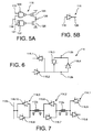
- the repetition devices 114 are made from repeaters 115.
- An exemplary repeater 115 is shown on FIG. Figure 5A .
- This repeater 115 has an input 118 connected to an input of a NAND gate 120 and to an input of a NOR gate 122.
- the data that the repeater transmits is applied to this input 118.
- the read / write signal is applied on the second input 119 of the NAND gate 120 and on a second input 121 of the NOR gate 122.
- the inverted output of the NAND gate 120 is connected to the gate of a first MOS transistor 124, and the output of the gate NOR 122 is connected to the gate of a second MOS transistor 126, the source of the first transistor 124 being connected to the drain of the second transistor 126 and forming an output 128 of the repeater 115.
- This repeater 115 may be represented by the symbol shown in FIG. Figure 5B .
- Such a repeater 115 outputs a bit of value identical to one bit applied as input.
- the level, or amplitude, of the output signal is constant and does not depend on the level of the input signal. Depending on the binary value of the read / write signal, the repeater 115 will or will not output a bit.
- the repetition devices 114 present on the vertical wire bundles 112b make it possible to repeat the information on these bundles of wires, but also to transmit the information from or to the memory blocks 106.
- An example of a repetition device 114 arranged on a vertical wire bundles 112b is shown on the figure 6 . It comprises two repeaters 115.1 and 115.2 arranged head-spades and connected in particular to the internal bus of the memory block 106.
- repeater 115.1, 115.2 are controlled by the value of the read / write signal, one being active while the other is inactive
- the repeater 115.1 is active when data is written in the memory block 106 (the output of the repeater 115.1 is connected to the data bus)
- the second repeater 115.2 is active when data is read from the memory block 106 (the input of the repeater 115.2 is connected to the data bus).
- the two repeaters 115.1, 115.2 is active during a read or write operation.
- Two other repeaters 115.3 and 115.4 form an interface between two segments of the vertical wire bundle 112b.
- repeaters 115.1, 115.2 only one of the two repeaters 115.3, 115.4 is active during the transmission of information, depending on whether the data transmitted are read or write data and depending on the location of the repeat device 114 on the vertical wire bundle 112b.
- the repetition devices 114 present on the horizontal wire bundles 112a allow either to transmit information between one of the processors 102 and a segment of one of the wire bundles 112a, or to repeat the information between two horizontal wire bundle segments. 112a. Alternatively, such a repetition device could also provide a repetition interface between one of the vertical wire bundles 112b and one of the horizontal wire bundles 112a.
- a first repeater 114.1 is provided for forming an interface between a horizontal wire harness segment 112a and one of the processors 102.
- the first repeater 114.1 includes a repeater 115.5 controlled by the read / write signal. and whose input is connected to the processor 102 and whose output is connected to the segment of the horizontal wire bundle 112a.
- This repeater 115.5 is active during an operation of writing information in one of the memory blocks 106, this information going from the processor to the memory block 106 of destination.
- This first repeater device 114.1 also comprises a second repeater 115.6 mounted upside down with respect to the repeater 115.5 and also controlled by the read / write signal, the input of which is connected to the segment of the wire harness horizontal 112a and the output to the processor 102.
- the second repeater 115.6 is active during an operation of reading information from one of the memory blocks 106, this information from the memory block 106 to the processor 102.
- This second repeater 115.6 could It should also be replaced by a NAND gate, one of whose inputs would be connected to the segment of the wire bundle 112a, the read / write signal being applied to a second input of this NAND gate, the output of which would be connected to the processor 102.
- a second repetition device 114.2 disposed between two segments of a horizontal wire bundle 112a, comprises two repeaters 115.7 and 115.8 mounted head-spades relative to each other and both controlled by the read signal / writing. Thus, one or other of these two repeaters 115.7, 115.8 is active according to whether a data read or write operation is performed.
- a third repetition device 114.3 for example similar to the repetition device 114.2, may be disposed between a segment of a horizontal wire bundle 112a and a segment of a vertical wire bundle 112b.
- Referees, or control devices are here generically designed by combinatorial logic elements. Thus, all the referees comprise the same logical structure made from identical logic circuits.
- a physical address for example hard coded in the memory 104, is assigned to each arbitrator according to its physical location in the memory, that is to say in depending on the location of the memory block 106 with which it is associated.
- the operation of the referees is governed by logic functions that activate only useful repetition devices, that is, those on the path between the processor and the memory block in which the information is read or written.
- the logical functions are such that the most direct path, that is to say the one requiring the least active repetition devices, is achieved by the activation of the good repetition devices.
- the minimum path between one of the processors 102 and one of the memory blocks 106 involves the activation of two repeat devices 114, one on one of the horizontal wire bundles 112a and one on one of the vertical wire bundles 112b.
- the maximum path corresponding to a communication between a processor located in one of the corners of the system and a memory block 106 located in the corner opposite to that where the processor is, involves the activation of five repetition devices 114 , two of which are on one of the horizontal wire bundles 112a and three on one of the vertical wire bundles 112b.
- the memory 104 comprises six memory blocks 106.
- each repeat device 114 disposed on one of the vertical wire bundles 112b is at a memory block 106, the values of the ADDB (1: 0) bits can be used to determine which devices repetition 114 disposed on the vertical wire bundle 112b must be activated.
- the power consumption of the interconnection network depends mainly on two factors: the activity rate of the network, which corresponds to the frequency of change of state (0 or 1 depending on the value of the signals) of the wires with respect to the frequency of operating clock, as well as the geographical location of the processor relative to the destination memory bank, that is to say the length of the communication path that is proportional to the number of repeat devices to be activated. It is also possible to further reduce the power consumption of the interconnection network 100 by optimizing the placement of the data in the memory blocks 106.
- the data relating to In this case can preferably be placed in a memory block 106 in the vicinity of this processor, thereby reducing the number of repeater devices to be activated to access this information.
- This optimization of the placement of the data in the memory blocks 106 may in particular be carried out by a code compiler when the data are, for example, machine code instructions stored in the memory 104.
Landscapes
- Engineering & Computer Science (AREA)
- Physics & Mathematics (AREA)
- General Engineering & Computer Science (AREA)
- Theoretical Computer Science (AREA)
- Mathematical Physics (AREA)
- Computer Hardware Design (AREA)
- General Physics & Mathematics (AREA)
- Multi Processors (AREA)
- Memory System (AREA)
- Bus Control (AREA)
- Data Exchanges In Wide-Area Networks (AREA)
Claims (11)
- Verbindungsnetz (100) zur Verbindung von m ersten elektronischen Schaltungen (102) mit n zweiten elektronischen Schaltungen (106), wobei es m Verbindungsunternetze aufweist, und wobei jedes Verbindungsunternetz aufweist,:- mindestens einen Adressbus und einen lnformationsübertragungsbus, der einen der m ersten Schaltungen (102) mit allen der n zweiten Schaltungen (106) verbindet, wobei der Informationsübertragungsbus eine Mehrzahl von Abschnitten von Signalübermittlungsleitungen (112a, 112b) aufweist, die mittels Signalwiederholungsvorrichtungen (114; 114.1 - 114.3) miteinander verbunden sind,- Einrichtungen zur Steuerung der Wiederholungsvorrichtungen (114; 114.1 - 114.3), die geeignet sind, mindestens eine der Wiederholungsvorrichtungen (114: 114.1 - 114.3) in Abhängigkeit vom Wert eines Adresssignals zu aktivieren, das dazu bestimmt ist, auf dem Adressbus durch die eine der m ersten Schaltungen (102) zu den Steuereinrichtungen gesendet zu werden, wobei die aktive Wiederholungsvorrichtung (114; 114.1 - 114.3) in dem Informationsübertragungsbus einen Datensignalkommunikationsweg zwischen der einen der m ersten Schaltungen (102) und mindestens einer der n zweiten Schaltungen (106), und/oder zwischen mindestens einer ersten der n zweiten Schaltungen (106) und mindestens einer zweiten der n zweiten Schaltungen (100) bildet,wobei m und n Ganzzahlen sind, die in jedem Fall größer als 1 sind.
- Verbindungsnetz (100) nach Anspruch 1, bei dem die m ersten Schaltungen (102) Prozessoren aufweisen und/oder die n zweiten Schaltungen (106) Speicherblöcke eines Speichers (104) aufweisen, den sich die m ersten Schaltungen (102) teilen.
- Verbindungsnetz (100) nach einem der vorhergehenden Ansprüche, bei dem die Signalwiederholungsvorrichtungen (114; 114.1-114.3) des informationsübertragungsbusses bidirektional sind.
- Verbindungsnetz (100) nach einem der vorhergehenden Ansprüche, bei dem der Adressbus eine Mehrzahl von Abschnitten von Signalübermittlungsleitungen aufweist, die miteinander durch Signalwiederholungsvorrichtungen verbunden sind.
- Verbindungsnetz (100) nach einem der vorhergehenden Ansprüche, bei dem die Signalwiederholungsvorrichtungen (114; 114.1 - 114.3) logische Schaltungen aufweisen.
- Verbindungsnetz (100) nach einem der vorhergehenden Ansprüche, bei dem die Steuereinrichtungen außerdem Einrichtungen zur Auswahl mindestens einer der n zweiten Schaltungen (106), um mindestens eine Operation zum Lesen und/oder Schreiben von Daten in der einen der n zweiten Schabungen (106) durchzuführen und/oder Einrichtungen zur Verwaltung der Priorität des Zugriffs auf die n zweiten Schaltungen (106) durch die m ersten Schaltungen (102) und/oder Einrichtungen zur Speicherung von mehreren Adressen von mehreren zweiten Schaltungen (106) aufweisen.
- Verbindungsnetz (100) nach einem der vorhergehenden Ansprüche, bei dem die Steuereinrichtungen eine Mehrzahl von Steuervorrichtungen aufweisen, wobei jede Steuervorrichtung geeignet ist, eine der Wiederholungsvorrichtungen (114; 114,1 - 114.3) in Abhängigkeit vom Wert des Adresssignals zu aktivieren oder zu deaktivieren.
- Verbindungsnetz (100) nach Anspruch 7, bei dem, wenn die n zweiten Schaltungen (106) Speicherblöcke eines geteilten Speichers (104) aufweisen, die Steuervorrichtungen im geteilten Speicher (104) implementiert sind.
- Verbindungsnetz (100) nach einem der Ansprüche 7 oder 8, bei dem die Steuereinrichtungen n Steuervorrichtungen aufweisen.
- Verbindungsnetz (100) nach einem der Ansprüche 7 bis 9, bei dem jede der Steuervorrichtungen ähnliche logische Schaltungen aufweiset, wobei ein eindeutig festgelegter Code dazu bestimmt ist, an den Eingang einer jeden Steuervorrichtung angelegt zu werden, um mindestens eine der n zweiten Schaltungen (106) zu identifizieren.
- Verbindungsnetz (100) nach einem der vorhergehenden Ansprüche, bei dem jedes Verbindungsunternetz einen zweiten Informationsübertragungsbus aufweist, der eine Mehrzahl von Abschnitten von Signalübermittlungsleitungen beinhaltet, die durch zweite Signalwiederholungsvorrichtungen miteinander verbunden sind, wobei die Steuereinrichtungen geeignet sind, mindestens eine der zweiten Wiederholungsvarrichtungen in Abhängigkeit vom Wert des Adresssignals zu aktivieren, wobei die zweite aktive Wiederhofungsvorrichtung im zweiten Informationsübertragungsbus einen Signalkommunikationsweg zwischen der einen der m ersten Schaltungen (102) und der einen der n zweiten Schaltungen (106) oder zwischen der einen ersten der n zweiten Schaltungen (106) und der einen zweiten der n zweiten Schaltungen (106) bildet.
Applications Claiming Priority (1)
| Application Number | Priority Date | Filing Date | Title |
|---|---|---|---|
| FR0953780A FR2946441A1 (fr) | 2009-06-08 | 2009-06-08 | Reseau d'interconnexions a sous-reseaux dynamiques. |
Publications (2)
| Publication Number | Publication Date |
|---|---|
| EP2264610A1 EP2264610A1 (de) | 2010-12-22 |
| EP2264610B1 true EP2264610B1 (de) | 2011-09-21 |
Family
ID=41479200
Family Applications (1)
| Application Number | Title | Priority Date | Filing Date |
|---|---|---|---|
| EP10164557A Not-in-force EP2264610B1 (de) | 2009-06-08 | 2010-06-01 | Verbindungsnetz mit dynamischen Unternetzen |
Country Status (5)
| Country | Link |
|---|---|
| US (1) | US8397009B2 (de) |
| EP (1) | EP2264610B1 (de) |
| JP (1) | JP5595796B2 (de) |
| AT (1) | ATE525699T1 (de) |
| FR (1) | FR2946441A1 (de) |
Families Citing this family (2)
| Publication number | Priority date | Publication date | Assignee | Title |
|---|---|---|---|---|
| FR2951868B1 (fr) * | 2009-10-28 | 2012-04-06 | Kalray | Briques de construction d'un reseau sur puce |
| JP6313237B2 (ja) | 2015-02-04 | 2018-04-18 | 東芝メモリ株式会社 | ストレージシステム |
Family Cites Families (16)
| Publication number | Priority date | Publication date | Assignee | Title |
|---|---|---|---|---|
| FR2036350A5 (de) * | 1969-03-12 | 1970-12-24 | Commissariat Energie Atomique | |
| DE3714385A1 (de) * | 1987-04-30 | 1988-11-10 | Philips Patentverwaltung | Verfahren und schaltungsanordnung zur koppelfeldsteuerung in einem vermittlungssystem |
| US5218240A (en) * | 1990-11-02 | 1993-06-08 | Concurrent Logic, Inc. | Programmable logic cell and array with bus repeaters |
| JPH06314264A (ja) * | 1993-05-06 | 1994-11-08 | Nec Corp | セルフ・ルーティング・クロスバー・スイッチ |
| US5602844A (en) * | 1994-11-15 | 1997-02-11 | Xerox Corporation | Self routing crossbar switch suitable for use as a switching fabric in an ATM switch |
| US5930256A (en) * | 1997-03-28 | 1999-07-27 | Xerox Corporation | Self-arbitrating crossbar switch |
| US6480927B1 (en) * | 1997-12-31 | 2002-11-12 | Unisys Corporation | High-performance modular memory system with crossbar connections |
| US6970967B2 (en) * | 2002-06-18 | 2005-11-29 | Texas Instruments Incorporated | Crossbar circuit having a plurality of repeaters forming different repeater arrangements |
| JP2006260127A (ja) * | 2005-03-17 | 2006-09-28 | Hiroshima Univ | 結合網およびそれを用いたマルチポートメモリ |
| KR100655081B1 (ko) * | 2005-12-22 | 2006-12-08 | 삼성전자주식회사 | 가변적 액세스 경로를 가지는 멀티 포트 반도체 메모리장치 및 그에 따른 방법 |
| US7769942B2 (en) * | 2006-07-27 | 2010-08-03 | Rambus, Inc. | Cross-threaded memory system |
| US7925816B2 (en) * | 2006-11-06 | 2011-04-12 | Oracle America, Inc. | Architecture for an output buffered switch with input groups |
| CA2705234A1 (en) * | 2007-11-09 | 2009-05-14 | Plurality Ltd. | Shared memory system for a tightly-coupled multiprocessor |
| JP5599969B2 (ja) * | 2008-03-19 | 2014-10-01 | ピーエスフォー ルクスコ エスエイアールエル | マルチポートメモリ、および該マルチポートメモリを備えるコンピュータシステム |
| US7791976B2 (en) * | 2008-04-24 | 2010-09-07 | Qualcomm Incorporated | Systems and methods for dynamic power savings in electronic memory operation |
| US8417863B2 (en) * | 2010-07-16 | 2013-04-09 | Apple Inc. | Synchronous bus driving with repeaters |
-
2009
- 2009-06-08 FR FR0953780A patent/FR2946441A1/fr not_active Withdrawn
-
2010
- 2010-06-01 EP EP10164557A patent/EP2264610B1/de not_active Not-in-force
- 2010-06-01 AT AT10164557T patent/ATE525699T1/de not_active IP Right Cessation
- 2010-06-02 US US12/792,218 patent/US8397009B2/en not_active Expired - Fee Related
- 2010-06-07 JP JP2010130027A patent/JP5595796B2/ja not_active Expired - Fee Related
Also Published As
| Publication number | Publication date |
|---|---|
| EP2264610A1 (de) | 2010-12-22 |
| US8397009B2 (en) | 2013-03-12 |
| FR2946441A1 (fr) | 2010-12-10 |
| JP5595796B2 (ja) | 2014-09-24 |
| ATE525699T1 (de) | 2011-10-15 |
| US20100312939A1 (en) | 2010-12-09 |
| JP2010282627A (ja) | 2010-12-16 |
Similar Documents
| Publication | Publication Date | Title |
|---|---|---|
| US11546272B2 (en) | Fabric interconnection for memory banks based on network-on-chip methodology | |
| FR2824157A1 (fr) | Systeme de memoire evolutif avec interconnexions reconfigurables | |
| US20160148901A1 (en) | Interconnect circuits at three-dimensional (3-d) bonding interfaces of a processor array | |
| CN117693812A (zh) | 测试以晶片上晶片方式接合的存储器及逻辑的存储器 | |
| CN101118782A (zh) | 存储和检索处理系统的数据的存储器系统和性能监视方法 | |
| FR2862147A1 (fr) | Reconfiguration dynamique de liaisons de type pci-express | |
| JP2010015654A (ja) | 電子回路装置 | |
| US20170124024A1 (en) | Array of processor core circuits with reversible tiers | |
| JP5533963B2 (ja) | 構成可能な入出力ポートを伴うメモリモジュール | |
| KR20230072318A (ko) | 웨이퍼-투-웨이퍼 본딩을 이용하는 스토리지 장치 및 그의 제조 방법 | |
| EP2264610B1 (de) | Verbindungsnetz mit dynamischen Unternetzen | |
| KR20100127317A (ko) | 멀티포트 메모리 슈퍼셀 및 데이터 경로 스위칭 회로를 갖는 집적 회로 | |
| WO2002003459A3 (en) | High-speed low-power semiconductor memory architecture | |
| FR2836732A1 (fr) | Dispositif et procedes pour interfacer une memoire cache | |
| EP0910021B1 (de) | Übertragungsvorrichtung zwischen mehreren Prozessoren | |
| US7596650B1 (en) | Increasing availability of input/output (I/O) interconnections in a system | |
| CN120276891A (zh) | 用于处理日志数据的装置、其操作方法和包括其的系统 | |
| EP1372074A1 (de) | System und Verfahren zur Ereignisverwaltung | |
| EP3557433A1 (de) | Steuerungsverfahren des routings von transaktionen zwischen mindestens einem quellgerät und mindestens einem zielgerät, beispielsweise zwischen einem multiport-speicher und einem entsprechenden chipsystem | |
| EP0822495B1 (de) | Auftragsverteilung in einem Mehrfachknoten-Rechnersystem | |
| EP4546150A1 (de) | Optimierung von datentransfers zwischen einem parallelverarbeitungsprozessor und einem speicher | |
| EP4273720B1 (de) | System on chip integriert eine direkte speicherzugriffschaltung und entsprechendes verfahren | |
| JP2020160755A (ja) | 半導体装置 | |
| FR2538140A1 (fr) | Dispositif de couplage de bus pour systeme de traitement de donnees a bus multiples | |
| WO2009053318A1 (fr) | Structure et procede de sauvegarde et de restitution de donnees |
Legal Events
| Date | Code | Title | Description |
|---|---|---|---|
| PUAI | Public reference made under article 153(3) epc to a published international application that has entered the european phase |
Free format text: ORIGINAL CODE: 0009012 |
|
| AK | Designated contracting states |
Kind code of ref document: A1 Designated state(s): AL AT BE BG CH CY CZ DE DK EE ES FI FR GB GR HR HU IE IS IT LI LT LU LV MC MK MT NL NO PL PT RO SE SI SK SM TR |
|
| AX | Request for extension of the european patent |
Extension state: BA ME RS |
|
| 17P | Request for examination filed |
Effective date: 20110128 |
|
| GRAP | Despatch of communication of intention to grant a patent |
Free format text: ORIGINAL CODE: EPIDOSNIGR1 |
|
| RIC1 | Information provided on ipc code assigned before grant |
Ipc: G06F 13/40 20060101AFI20110301BHEP |
|
| GRAS | Grant fee paid |
Free format text: ORIGINAL CODE: EPIDOSNIGR3 |
|
| GRAA | (expected) grant |
Free format text: ORIGINAL CODE: 0009210 |
|
| AK | Designated contracting states |
Kind code of ref document: B1 Designated state(s): AL AT BE BG CH CY CZ DE DK EE ES FI FR GB GR HR HU IE IS IT LI LT LU LV MC MK MT NL NO PL PT RO SE SI SK SM TR |
|
| REG | Reference to a national code |
Ref country code: GB Ref legal event code: FG4D Free format text: NOT ENGLISH |
|
| REG | Reference to a national code |
Ref country code: CH Ref legal event code: EP |
|
| REG | Reference to a national code |
Ref country code: IE Ref legal event code: FG4D Free format text: LANGUAGE OF EP DOCUMENT: FRENCH |
|
| REG | Reference to a national code |
Ref country code: DE Ref legal event code: R096 Ref document number: 602010000206 Country of ref document: DE Effective date: 20111117 |
|
| REG | Reference to a national code |
Ref country code: NL Ref legal event code: VDEP Effective date: 20110921 |
|
| PG25 | Lapsed in a contracting state [announced via postgrant information from national office to epo] |
Ref country code: FI Free format text: LAPSE BECAUSE OF FAILURE TO SUBMIT A TRANSLATION OF THE DESCRIPTION OR TO PAY THE FEE WITHIN THE PRESCRIBED TIME-LIMIT Effective date: 20110921 Ref country code: SE Free format text: LAPSE BECAUSE OF FAILURE TO SUBMIT A TRANSLATION OF THE DESCRIPTION OR TO PAY THE FEE WITHIN THE PRESCRIBED TIME-LIMIT Effective date: 20110921 Ref country code: LT Free format text: LAPSE BECAUSE OF FAILURE TO SUBMIT A TRANSLATION OF THE DESCRIPTION OR TO PAY THE FEE WITHIN THE PRESCRIBED TIME-LIMIT Effective date: 20110921 Ref country code: HR Free format text: LAPSE BECAUSE OF FAILURE TO SUBMIT A TRANSLATION OF THE DESCRIPTION OR TO PAY THE FEE WITHIN THE PRESCRIBED TIME-LIMIT Effective date: 20110921 Ref country code: NO Free format text: LAPSE BECAUSE OF FAILURE TO SUBMIT A TRANSLATION OF THE DESCRIPTION OR TO PAY THE FEE WITHIN THE PRESCRIBED TIME-LIMIT Effective date: 20111221 |
|
| LTIE | Lt: invalidation of european patent or patent extension |
Effective date: 20110921 |
|
| PG25 | Lapsed in a contracting state [announced via postgrant information from national office to epo] |
Ref country code: GR Free format text: LAPSE BECAUSE OF FAILURE TO SUBMIT A TRANSLATION OF THE DESCRIPTION OR TO PAY THE FEE WITHIN THE PRESCRIBED TIME-LIMIT Effective date: 20111222 Ref country code: SI Free format text: LAPSE BECAUSE OF FAILURE TO SUBMIT A TRANSLATION OF THE DESCRIPTION OR TO PAY THE FEE WITHIN THE PRESCRIBED TIME-LIMIT Effective date: 20110921 Ref country code: AT Free format text: LAPSE BECAUSE OF FAILURE TO SUBMIT A TRANSLATION OF THE DESCRIPTION OR TO PAY THE FEE WITHIN THE PRESCRIBED TIME-LIMIT Effective date: 20110921 Ref country code: CY Free format text: LAPSE BECAUSE OF FAILURE TO SUBMIT A TRANSLATION OF THE DESCRIPTION OR TO PAY THE FEE WITHIN THE PRESCRIBED TIME-LIMIT Effective date: 20110921 Ref country code: LV Free format text: LAPSE BECAUSE OF FAILURE TO SUBMIT A TRANSLATION OF THE DESCRIPTION OR TO PAY THE FEE WITHIN THE PRESCRIBED TIME-LIMIT Effective date: 20110921 |
|
| REG | Reference to a national code |
Ref country code: AT Ref legal event code: MK05 Ref document number: 525699 Country of ref document: AT Kind code of ref document: T Effective date: 20110921 |
|
| REG | Reference to a national code |
Ref country code: IE Ref legal event code: FD4D |
|
| PG25 | Lapsed in a contracting state [announced via postgrant information from national office to epo] |
Ref country code: CZ Free format text: LAPSE BECAUSE OF FAILURE TO SUBMIT A TRANSLATION OF THE DESCRIPTION OR TO PAY THE FEE WITHIN THE PRESCRIBED TIME-LIMIT Effective date: 20110921 Ref country code: IE Free format text: LAPSE BECAUSE OF FAILURE TO SUBMIT A TRANSLATION OF THE DESCRIPTION OR TO PAY THE FEE WITHIN THE PRESCRIBED TIME-LIMIT Effective date: 20110921 Ref country code: SK Free format text: LAPSE BECAUSE OF FAILURE TO SUBMIT A TRANSLATION OF THE DESCRIPTION OR TO PAY THE FEE WITHIN THE PRESCRIBED TIME-LIMIT Effective date: 20110921 Ref country code: IS Free format text: LAPSE BECAUSE OF FAILURE TO SUBMIT A TRANSLATION OF THE DESCRIPTION OR TO PAY THE FEE WITHIN THE PRESCRIBED TIME-LIMIT Effective date: 20120121 |
|
| PG25 | Lapsed in a contracting state [announced via postgrant information from national office to epo] |
Ref country code: PT Free format text: LAPSE BECAUSE OF FAILURE TO SUBMIT A TRANSLATION OF THE DESCRIPTION OR TO PAY THE FEE WITHIN THE PRESCRIBED TIME-LIMIT Effective date: 20120123 Ref country code: PL Free format text: LAPSE BECAUSE OF FAILURE TO SUBMIT A TRANSLATION OF THE DESCRIPTION OR TO PAY THE FEE WITHIN THE PRESCRIBED TIME-LIMIT Effective date: 20110921 Ref country code: EE Free format text: LAPSE BECAUSE OF FAILURE TO SUBMIT A TRANSLATION OF THE DESCRIPTION OR TO PAY THE FEE WITHIN THE PRESCRIBED TIME-LIMIT Effective date: 20110921 Ref country code: NL Free format text: LAPSE BECAUSE OF FAILURE TO SUBMIT A TRANSLATION OF THE DESCRIPTION OR TO PAY THE FEE WITHIN THE PRESCRIBED TIME-LIMIT Effective date: 20110921 Ref country code: RO Free format text: LAPSE BECAUSE OF FAILURE TO SUBMIT A TRANSLATION OF THE DESCRIPTION OR TO PAY THE FEE WITHIN THE PRESCRIBED TIME-LIMIT Effective date: 20110921 |
|
| PLBE | No opposition filed within time limit |
Free format text: ORIGINAL CODE: 0009261 |
|
| STAA | Information on the status of an ep patent application or granted ep patent |
Free format text: STATUS: NO OPPOSITION FILED WITHIN TIME LIMIT |
|
| PG25 | Lapsed in a contracting state [announced via postgrant information from national office to epo] |
Ref country code: DK Free format text: LAPSE BECAUSE OF FAILURE TO SUBMIT A TRANSLATION OF THE DESCRIPTION OR TO PAY THE FEE WITHIN THE PRESCRIBED TIME-LIMIT Effective date: 20110921 |
|
| 26N | No opposition filed |
Effective date: 20120622 |
|
| REG | Reference to a national code |
Ref country code: DE Ref legal event code: R097 Ref document number: 602010000206 Country of ref document: DE Effective date: 20120622 |
|
| BERE | Be: lapsed |
Owner name: COMMISSARIAT A L'ENERGIE ATOMIQUE ET AUX ENERGIES Effective date: 20120630 |
|
| PG25 | Lapsed in a contracting state [announced via postgrant information from national office to epo] |
Ref country code: MC Free format text: LAPSE BECAUSE OF NON-PAYMENT OF DUE FEES Effective date: 20120630 |
|
| PG25 | Lapsed in a contracting state [announced via postgrant information from national office to epo] |
Ref country code: MK Free format text: LAPSE BECAUSE OF FAILURE TO SUBMIT A TRANSLATION OF THE DESCRIPTION OR TO PAY THE FEE WITHIN THE PRESCRIBED TIME-LIMIT Effective date: 20110921 |
|
| PG25 | Lapsed in a contracting state [announced via postgrant information from national office to epo] |
Ref country code: ES Free format text: LAPSE BECAUSE OF FAILURE TO SUBMIT A TRANSLATION OF THE DESCRIPTION OR TO PAY THE FEE WITHIN THE PRESCRIBED TIME-LIMIT Effective date: 20120101 Ref country code: BE Free format text: LAPSE BECAUSE OF NON-PAYMENT OF DUE FEES Effective date: 20120630 |
|
| PG25 | Lapsed in a contracting state [announced via postgrant information from national office to epo] |
Ref country code: BG Free format text: LAPSE BECAUSE OF FAILURE TO SUBMIT A TRANSLATION OF THE DESCRIPTION OR TO PAY THE FEE WITHIN THE PRESCRIBED TIME-LIMIT Effective date: 20111221 |
|
| PG25 | Lapsed in a contracting state [announced via postgrant information from national office to epo] |
Ref country code: MT Free format text: LAPSE BECAUSE OF FAILURE TO SUBMIT A TRANSLATION OF THE DESCRIPTION OR TO PAY THE FEE WITHIN THE PRESCRIBED TIME-LIMIT Effective date: 20110921 |
|
| PG25 | Lapsed in a contracting state [announced via postgrant information from national office to epo] |
Ref country code: AL Free format text: LAPSE BECAUSE OF FAILURE TO SUBMIT A TRANSLATION OF THE DESCRIPTION OR TO PAY THE FEE WITHIN THE PRESCRIBED TIME-LIMIT Effective date: 20110921 |
|
| PG25 | Lapsed in a contracting state [announced via postgrant information from national office to epo] |
Ref country code: TR Free format text: LAPSE BECAUSE OF FAILURE TO SUBMIT A TRANSLATION OF THE DESCRIPTION OR TO PAY THE FEE WITHIN THE PRESCRIBED TIME-LIMIT Effective date: 20110921 |
|
| PG25 | Lapsed in a contracting state [announced via postgrant information from national office to epo] |
Ref country code: LU Free format text: LAPSE BECAUSE OF NON-PAYMENT OF DUE FEES Effective date: 20120601 Ref country code: SM Free format text: LAPSE BECAUSE OF FAILURE TO SUBMIT A TRANSLATION OF THE DESCRIPTION OR TO PAY THE FEE WITHIN THE PRESCRIBED TIME-LIMIT Effective date: 20110921 |
|
| PG25 | Lapsed in a contracting state [announced via postgrant information from national office to epo] |
Ref country code: HU Free format text: LAPSE BECAUSE OF FAILURE TO SUBMIT A TRANSLATION OF THE DESCRIPTION OR TO PAY THE FEE WITHIN THE PRESCRIBED TIME-LIMIT Effective date: 20100601 |
|
| REG | Reference to a national code |
Ref country code: CH Ref legal event code: PL |
|
| PG25 | Lapsed in a contracting state [announced via postgrant information from national office to epo] |
Ref country code: CH Free format text: LAPSE BECAUSE OF NON-PAYMENT OF DUE FEES Effective date: 20140630 Ref country code: LI Free format text: LAPSE BECAUSE OF NON-PAYMENT OF DUE FEES Effective date: 20140630 |
|
| REG | Reference to a national code |
Ref country code: FR Ref legal event code: PLFP Year of fee payment: 6 |
|
| PGFP | Annual fee paid to national office [announced via postgrant information from national office to epo] |
Ref country code: GB Payment date: 20150619 Year of fee payment: 6 Ref country code: DE Payment date: 20150612 Year of fee payment: 6 |
|
| PGFP | Annual fee paid to national office [announced via postgrant information from national office to epo] |
Ref country code: IT Payment date: 20150612 Year of fee payment: 6 |
|
| PGFP | Annual fee paid to national office [announced via postgrant information from national office to epo] |
Ref country code: FR Payment date: 20150630 Year of fee payment: 6 |
|
| REG | Reference to a national code |
Ref country code: DE Ref legal event code: R119 Ref document number: 602010000206 Country of ref document: DE |
|
| GBPC | Gb: european patent ceased through non-payment of renewal fee |
Effective date: 20160601 |
|
| REG | Reference to a national code |
Ref country code: FR Ref legal event code: ST Effective date: 20170228 |
|
| PG25 | Lapsed in a contracting state [announced via postgrant information from national office to epo] |
Ref country code: FR Free format text: LAPSE BECAUSE OF NON-PAYMENT OF DUE FEES Effective date: 20160630 Ref country code: DE Free format text: LAPSE BECAUSE OF NON-PAYMENT OF DUE FEES Effective date: 20170103 |
|
| PG25 | Lapsed in a contracting state [announced via postgrant information from national office to epo] |
Ref country code: GB Free format text: LAPSE BECAUSE OF NON-PAYMENT OF DUE FEES Effective date: 20160601 |
|
| PG25 | Lapsed in a contracting state [announced via postgrant information from national office to epo] |
Ref country code: IT Free format text: LAPSE BECAUSE OF NON-PAYMENT OF DUE FEES Effective date: 20160601 |