EP2256782B1 - Plasma deposition source and method for depositing thin films - Google Patents
Plasma deposition source and method for depositing thin films Download PDFInfo
- Publication number
- EP2256782B1 EP2256782B1 EP09161034.5A EP09161034A EP2256782B1 EP 2256782 B1 EP2256782 B1 EP 2256782B1 EP 09161034 A EP09161034 A EP 09161034A EP 2256782 B1 EP2256782 B1 EP 2256782B1
- Authority
- EP
- European Patent Office
- Prior art keywords
- electrode
- plasma
- substrate
- gas
- deposition
- Prior art date
- Legal status (The legal status is an assumption and is not a legal conclusion. Google has not performed a legal analysis and makes no representation as to the accuracy of the status listed.)
- Not-in-force
Links
- 238000000151 deposition Methods 0.000 title claims description 144
- 230000008021 deposition Effects 0.000 title claims description 124
- 238000000034 method Methods 0.000 title claims description 44
- 239000010409 thin film Substances 0.000 title claims description 33
- 239000000758 substrate Substances 0.000 claims description 182
- 239000002245 particle Substances 0.000 claims description 6
- 230000005684 electric field Effects 0.000 claims description 3
- 239000007789 gas Substances 0.000 description 195
- BLRPTPMANUNPDV-UHFFFAOYSA-N Silane Chemical compound [SiH4] BLRPTPMANUNPDV-UHFFFAOYSA-N 0.000 description 55
- 229910000077 silane Inorganic materials 0.000 description 42
- 230000004048 modification Effects 0.000 description 24
- 238000012986 modification Methods 0.000 description 24
- 230000008569 process Effects 0.000 description 24
- 239000002243 precursor Substances 0.000 description 18
- 238000000623 plasma-assisted chemical vapour deposition Methods 0.000 description 15
- 230000015572 biosynthetic process Effects 0.000 description 11
- 238000005137 deposition process Methods 0.000 description 11
- 239000000428 dust Substances 0.000 description 11
- XUIMIQQOPSSXEZ-UHFFFAOYSA-N Silicon Chemical compound [Si] XUIMIQQOPSSXEZ-UHFFFAOYSA-N 0.000 description 9
- 239000010408 film Substances 0.000 description 9
- 239000000203 mixture Substances 0.000 description 9
- 229910052710 silicon Inorganic materials 0.000 description 9
- 239000010703 silicon Substances 0.000 description 9
- 229910021424 microcrystalline silicon Inorganic materials 0.000 description 8
- 238000009826 distribution Methods 0.000 description 7
- 229910003828 SiH3 Inorganic materials 0.000 description 6
- OLRJXMHANKMLTD-UHFFFAOYSA-N silyl Chemical compound [SiH3] OLRJXMHANKMLTD-UHFFFAOYSA-N 0.000 description 6
- 238000005086 pumping Methods 0.000 description 5
- 230000004913 activation Effects 0.000 description 4
- 239000000956 alloy Substances 0.000 description 4
- 230000008901 benefit Effects 0.000 description 4
- 239000011248 coating agent Substances 0.000 description 4
- 238000000576 coating method Methods 0.000 description 4
- 239000002210 silicon-based material Substances 0.000 description 4
- 229910021417 amorphous silicon Inorganic materials 0.000 description 3
- 230000007423 decrease Effects 0.000 description 3
- 238000013461 design Methods 0.000 description 3
- 238000004519 manufacturing process Methods 0.000 description 3
- 239000000047 product Substances 0.000 description 3
- 238000000427 thin-film deposition Methods 0.000 description 3
- 238000012546 transfer Methods 0.000 description 3
- 238000001069 Raman spectroscopy Methods 0.000 description 2
- 230000008859 change Effects 0.000 description 2
- 239000007795 chemical reaction product Substances 0.000 description 2
- 230000009849 deactivation Effects 0.000 description 2
- 238000000354 decomposition reaction Methods 0.000 description 2
- 238000005530 etching Methods 0.000 description 2
- 239000011521 glass Substances 0.000 description 2
- 239000001257 hydrogen Substances 0.000 description 2
- 229910052739 hydrogen Inorganic materials 0.000 description 2
- 238000012423 maintenance Methods 0.000 description 2
- 239000000463 material Substances 0.000 description 2
- 238000004377 microelectronic Methods 0.000 description 2
- 230000009467 reduction Effects 0.000 description 2
- 239000004065 semiconductor Substances 0.000 description 2
- 150000003376 silicon Chemical class 0.000 description 2
- UFHFLCQGNIYNRP-UHFFFAOYSA-N Hydrogen Chemical compound [H][H] UFHFLCQGNIYNRP-UHFFFAOYSA-N 0.000 description 1
- 229910000676 Si alloy Inorganic materials 0.000 description 1
- 229910045601 alloy Inorganic materials 0.000 description 1
- QVGXLLKOCUKJST-UHFFFAOYSA-N atomic oxygen Chemical compound [O] QVGXLLKOCUKJST-UHFFFAOYSA-N 0.000 description 1
- 239000000356 contaminant Substances 0.000 description 1
- 238000011109 contamination Methods 0.000 description 1
- 229910021419 crystalline silicon Inorganic materials 0.000 description 1
- 230000003247 decreasing effect Effects 0.000 description 1
- 230000002939 deleterious effect Effects 0.000 description 1
- 230000001419 dependent effect Effects 0.000 description 1
- 230000000694 effects Effects 0.000 description 1
- 230000005284 excitation Effects 0.000 description 1
- 239000000284 extract Substances 0.000 description 1
- 239000011888 foil Substances 0.000 description 1
- 238000011835 investigation Methods 0.000 description 1
- 238000002955 isolation Methods 0.000 description 1
- 239000001301 oxygen Substances 0.000 description 1
- 229910052760 oxygen Inorganic materials 0.000 description 1
- 238000002161 passivation Methods 0.000 description 1
- 238000005268 plasma chemical vapour deposition Methods 0.000 description 1
- 238000001020 plasma etching Methods 0.000 description 1
- 239000010453 quartz Substances 0.000 description 1
- 238000000926 separation method Methods 0.000 description 1
- VYPSYNLAJGMNEJ-UHFFFAOYSA-N silicon dioxide Inorganic materials O=[Si]=O VYPSYNLAJGMNEJ-UHFFFAOYSA-N 0.000 description 1
- 239000007787 solid Substances 0.000 description 1
- 238000001228 spectrum Methods 0.000 description 1
- 230000006641 stabilisation Effects 0.000 description 1
- 238000011105 stabilization Methods 0.000 description 1
- 239000000126 substance Substances 0.000 description 1
Images


Classifications
-
- H—ELECTRICITY
- H01—ELECTRIC ELEMENTS
- H01J—ELECTRIC DISCHARGE TUBES OR DISCHARGE LAMPS
- H01J37/00—Discharge tubes with provision for introducing objects or material to be exposed to the discharge, e.g. for the purpose of examination or processing thereof
- H01J37/32—Gas-filled discharge tubes
-
- C—CHEMISTRY; METALLURGY
- C23—COATING METALLIC MATERIAL; COATING MATERIAL WITH METALLIC MATERIAL; CHEMICAL SURFACE TREATMENT; DIFFUSION TREATMENT OF METALLIC MATERIAL; COATING BY VACUUM EVAPORATION, BY SPUTTERING, BY ION IMPLANTATION OR BY CHEMICAL VAPOUR DEPOSITION, IN GENERAL; INHIBITING CORROSION OF METALLIC MATERIAL OR INCRUSTATION IN GENERAL
- C23C—COATING METALLIC MATERIAL; COATING MATERIAL WITH METALLIC MATERIAL; SURFACE TREATMENT OF METALLIC MATERIAL BY DIFFUSION INTO THE SURFACE, BY CHEMICAL CONVERSION OR SUBSTITUTION; COATING BY VACUUM EVAPORATION, BY SPUTTERING, BY ION IMPLANTATION OR BY CHEMICAL VAPOUR DEPOSITION, IN GENERAL
- C23C14/00—Coating by vacuum evaporation, by sputtering or by ion implantation of the coating forming material
- C23C14/22—Coating by vacuum evaporation, by sputtering or by ion implantation of the coating forming material characterised by the process of coating
- C23C14/50—Substrate holders
- C23C14/505—Substrate holders for rotation of the substrates
-
- H—ELECTRICITY
- H01—ELECTRIC ELEMENTS
- H01J—ELECTRIC DISCHARGE TUBES OR DISCHARGE LAMPS
- H01J37/00—Discharge tubes with provision for introducing objects or material to be exposed to the discharge, e.g. for the purpose of examination or processing thereof
- H01J37/32—Gas-filled discharge tubes
- H01J37/32009—Arrangements for generation of plasma specially adapted for examination or treatment of objects, e.g. plasma sources
- H01J37/32082—Radio frequency generated discharge
-
- H—ELECTRICITY
- H01—ELECTRIC ELEMENTS
- H01J—ELECTRIC DISCHARGE TUBES OR DISCHARGE LAMPS
- H01J37/00—Discharge tubes with provision for introducing objects or material to be exposed to the discharge, e.g. for the purpose of examination or processing thereof
- H01J37/32—Gas-filled discharge tubes
- H01J37/32431—Constructional details of the reactor
- H01J37/32733—Means for moving the material to be treated
- H01J37/32752—Means for moving the material to be treated for moving the material across the discharge
- H01J37/32761—Continuous moving
- H01J37/3277—Continuous moving of continuous material
Definitions
- Embodiments of the present invention relate to a plasma enhanced chemical vapor deposition system for depositing thin films onto substrates.
- embodiments relate to a plasma deposition source for transferring a deposition gas into a plasma phase by means of RF (radio frequency) electrodes.
- the present invention relates to a method for depositing thin films onto a moving substrate.
- PECVD plasma-enhanced chemical vapor deposition
- This type of thin film deposition has many applications, e.g. in the microelectronic industry, for depositing photovoltaic layers onto flexible substrates, for modifying surfaces of substrates in general, etc.
- Silicon-based deposition gases are used e.g. for the fabrication of thin silicon films on substrates for manufacturing of photovoltaic cells.
- Deposition gases which are used to deposit silicon-based materials onto substrates typically include silane or silane-based precursor gases.
- document EP 0 942 473 A describes a process for forming a microcrystalline silicon series thin film by arranging a long substrate in a vacuum chamber so as to oppose an electrode provided in said vacuum chamber and while transporting said long substrate in a longitudinal direction, causing glow discharge between said electrode and said long substrate to deposit said microcrystalline silicon series thin film on said long substrate, wherein a plurality of bar-like shaped electrodes as said electrode are arranged such that they are perpendicular to a normal line of said long substrate and their intervals to said long substrate are all or partially differed.
- document WO 92/15722 A describes a continuous apparatus for the glow discharge deposition of amorphous silicon alloy solar cells of p-i-n-type configuration in a plurality of interconnected, dedicated deposition chambers, a plasma bar operatively disposed between at least the plasma regions in which the layer pairs of amorphous silicon alloy material defining the major semiconductor junction of the solar cell are deposited.
- the plasma bar is adapted to initiate a plasma so as to prevent chemically adsorbed contaminants from deleteriously affecting the surface of the first deposited of the layer pair, thereby improving the open circuit voltage of the solar cell.
- the plasma bar may also be provided between the layer pairs of amorphous silicon alloy material which combine to define the minor semiconductor junction of the solar cell.
- a plasma bar may be disposed between the oxide-based layer of a back reflector for reducing oxygen contamination of the silicon alloy material deposited thereupon.
- document to provide a method and device for forming a plasma CVD film of high throughput capable of realizing a high film forming rate The faces to be film-formed in substrates to be passed through substrate transferring lines are proximately confronted with the circumferential faces of plural rotary drum electrodes, the rotary drum electrodes are respectively positioned to the substrate transferring lines, a stage in which each rotary drum electrode is rotated, a stage in which, in such a manner that the circumferential face of each rotary drum electrode in the process of rotation is proximately confronted with the face to be film-formed in the substrate, the substrate is transferred along the substrate transferring line, and a stage in which reactive gas is fed to the space between each rotary drum electrode in the process of rotation and the substrate in the process of transfer, furthermore, each rotary drum electrode is applied with high frequency to generate plasma in the space between each rotary drum electrode in the process of rotation and the substrate in the process of transfer, and the substrate in the process of transfer is continuously film-formed
- a formation of silane dust is deleterious for the thin film being deposited.
- a more efficient deposition of thin films onto substrates is based on an increase in the deposition rate and a reduction of the formation of dust (silane dust, etc.).
- Linear PECVD sources may be used for a dynamic deposition of silicon-based materials for photovoltaic deposition applications. Additionally, costs for manufacturing photovoltaic or microelectronic components based on a deposition of thin films increase if a plasma deposition system has a reduced uptime due to unwanted dust formation. The greater the formation of dust is, the shorter time intervals between maintenance are for the entire PECVD system.
- US 2008/096305 A1 discloses a method for forming a deposited film containing microcrystalline silicon on a moving substrate by plasma-enhanced CVD includes forming a deposited film containing microcrystalline silicon on a moving substrate by plasma-enhanced CVD under conditions such that when a deposited film having a thickness of 300 nm or more is formed on a substrate while the substrate is in a stationary state, an area of the microcrystalline silicon region in which an intensity of Raman scattering attributed to a crystalline substance in the deposited film is equal to or higher than three times an intensity of Raman scattering attributed to an amorphous is 50% or more of the total area based on the area of the microcrystalline silicon region and the area of a region composed of the amorphous.
- a plasma deposition source for transferring a deposition gas into a plasma phase and for depositing, from the plasma phase, a thin film onto a substrate moving in a substrate transport direction in a vacuum chamber according to independent claim 1 is provided. Furthermore, a method for depositing a thin film onto a substrate according to independent claim 8 is provided.
- Embodiments described herein refer inter alia to a plasma deposition system for depositing, from a plasma phase, thin films onto a moving substrate.
- the substrate may move in a substrate transport direction in a vacuum chamber where a plasma deposition source for transferring a deposition gas into a plasma phase and for depositing, from the plasma phase, a thin film onto the moving substrate is located.
- a plasma deposition source 100 is provided as a linear PECVD (plasma-enhanced chemical vapor deposition) source having a multi-region electrode device 300 including three RF electrodes 301 arranged opposite to a moving substrate 500.
- the multi-region electrode device 300 is shown to be positioned over the substrate 500 moving in a substrate transport direction 501.
- the plasma deposition source can be adapted for depositing a thin film on a flexible substrate, e.g., a web or a foil, a glass substrate or silicon substrate.
- the plasma deposition source can be adapted for and can be used for depositing a thin film on a flexible substrate, e.g., to form a flexible PV module.
- a flexible substrate e.g., a web or a foil, a glass substrate or silicon substrate.
- the plasma deposition source can be adapted for and can be used for depositing a thin film on a flexible substrate, e.g., to form a flexible PV module.
- an efficient deposition can be provided for the opportunity to deposit different layers with significantly different film thicknesses.
- the individual RF electrodes 301 each have an electrode width 304 and an electrode length 305, wherein the electrode width is measured in a direction parallel to the substrate transport direction 501 and wherein the electrode length 305 is measured in a direction perpendicular to the substrate transport direction 501 of the moving substrate 500.
- three RF electrodes 301 may have the same electrode width 304 and electrode length 305 such that an electrode area of all electrodes is the same.
- the electrode area corresponds to a plasma region such that the plasma regions of the at least two electrodes 301 form a combined plasma region, which is located in one vacuum chamber.
- a multi-region electrode device 300 is formed, which is located in one vacuum chamber.
- one vacuum chamber is to be understood as a region not being separated by pressure apertures, valves or other elements for providing different pressures or different atmospheres in areas of a vacuum system.
- the pressure may be in a range from 0.01 mbar to 4.0 mbar.
- the electrode width 304 may be determined on the basis of plasma parameters such as deposition gas flow, plasma pressure, RF power and RF frequency provided at the respective RF electrode, and a deposition gas depletion profile. A determination of the electrode width 304 of the individual RF electrodes will be described herein below with respect to FIG. 3 and FIG. 4 .
- the electrode length 305 of an individual RF electrode 301 may be adjusted such that the electrode length 305 exceeds a lateral dimension of the moving substrate 500 perpendicular to the substrate transport direction 501.
- the electrode length 305 may be larger than the electrode width 304.
- the electrode width 304 may depend on an RF frequency which is used for a specific plasma deposition process.
- plasma deposition source in accordance with embodiments described herein may also be used for plasma enhanced etching processes, plasma-enhanced surface modification processes, plasma-enhanced surface activation or deactivation processes, and other plasma-enhanced processes known to the skilled person.
- the substrate transport direction 501 is parallel to a gas flow direction 203.
- gas inlets and gas outlets are arranged.
- the gas inlets or gas outlets may be provided as gas lances, gas channels, gas ducts, gas passages, gas tubes, conduits, etc..
- a gas outlet may be configured as a part of a pump which extracts gas from the plasma volume.
- At least one gas inlet 201 is arranged at an electrode leading edge 302 and at least one gas outlet 202 is arranged at an electrode trailing edge 303 of an individual RF electrode 301 of the multi-region electrode device 300.
- the electrode leading edge 302 and the electrode trailing edge 303 are defined with respect to the substrate transport direction 501.
- the gas inlet 201 might be disposed at the trailing edge and the gas outlet 202 might be disposed at the leading edge.
- the embodiment shown in FIG. 1 exhibits a gas flow direction 203 parallel to the substrate transport direction 501
- the gas flow direction 203 is anti-parallel to the substrate transport direction by exchanging the respective positions of the gas inlet 201 and the gas outlet 202 of the respective RF electrode 301.
- an alternating gas flow direction 203 from one RF electrode 301 to an adjacent RF electrode 301 may be provided.
- gas inlet denotes a gas supply into a deposition region (a plasma volume 101)
- gas outlet denotes a gas discharge or evacuation of deposition gas out of a deposition region.
- the gas inlet 201 and the gas outlet 202 according to a typical embodiment are arranged essentially perpendicular to the substrate transport direction 501.
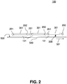
- FIG. 2 is a schematic side cross-sectional view of the plasma deposition source 100 shown in FIG. 1 .
- a plasma is formed in a plasma volume 101 which is located between a lower surface of an individual RF electrode 301 and a substrate surface to be coated 502, which is adjacent to a counter electrode 406 (see Fig. 6 ) for plasma generation.
- the substrate 500 to be coated is transported from left to right in the substrate transport direction 501.
- the individual gas inlets 201 and the individual gas outlets 202 are provided for a leading edge 302 (left edge in FIG.
- a gas flow underneath the RF electrode is provided from the gas inlet 301 to the gas outlet 202 such that a gas flow direction 203 (see FIG. 1 ) is essentially parallel to the substrate transport direction 501. Furthermore, it is possible, albeit not shown in FIG. 2 , that a gas flow direction is anti-parallel to the substrate transport direction 501. To provide such kind of anti-parallel gas flow at an individual RF electrode 301, the gas inlet 201 and the gas outlet 202 at the respective RF electrode 301 are exchanged with respect to each other, according to a further typical embodiment.
- embodiments described herein are adapted for and allow for a multi.-electrode device wherein the gas flow direction with regard to the transport direction of the substrate is the same direction or an opposite direction, i.e. the gas flow direction and the transport direction are essentially parallel or essentially anti-parallel.
- a multi-region electrode device can be easily up-scaled to four, five, six or even more electrodes without significantly changing the plasma process parameters in the entire, combined plasma region.
- a wide variety of thin film deposition processes may be performed by using the plasma deposition source 100 having at least one RF electrode 301.
- the substrate surface 502 may be provided with a thin film while the substrate 500 is moving in the substrate transport direction 501.
- the thin film may be provided by means of any material which can be transferred into a plasma phase by the deposition source 100.
- thin films and thin solid films may be deposited onto the substrate surface 502.
- the electrode cross-sectional shape of at least one RF electrode 301 may be adapted to a surface shape of a substrate surface 502 to be coated.
- the lower surface of an individual RF electrode 301 faces the substrate surface 502 to be coated such that the plasma volume 101 which is provided between an individual RF electrode 301 and the substrate 500 may be controlled.
- a distance between the lower surface of the RF electrode 301 and the substrate surface 502 to be coated is referred to as an electrode-substrate gap distance 308 in FIG. 2 .
- the plasma volume 101 is essentially defined by a (geometrical) product of the electrode length 305, the electrode width 304 (see FIG. 1 ) and the electrode-substrate gap distance 308.
- An individual RF electrode 301 has an electrode length 305 oriented perpendicular to the substrate transport direction 501 which is at least a substrate width of the moving substrate perpendicular to the substrate transport direction 501.
- a normalized plasma volume may be defined by dividing the plasma volume 101 provided between the lower electrode surface and the opposite substrate surface 502, by the electrode length 305. The normalized plasma volume then is given on the basis of a deposition gas flow, a plasma pressure, an RF power applied at an individual RF electrode 301 and a RF frequency provided at the RF electrode 301.
- an electrode width 304 of an individual RF electrode 301 may be adjusted such that an electrode width 304 parallel to the substrate transport direction 501 is given by the normalized plasma volume divided by the electrode-substrate gap distance 308 shown in FIG. 2 .
- the normalized plasma volume may be in the range from 5 cm 2 to 50 cm 2
- a plasma density for a silicon-based PECVD process may be in a range from 10 9 cm 3 to 10 11 cm 3
- electron temperatures may range from 1 eV to 3 eV, respectively.
- the flow rates of silane (SiH4) for the silicon-based PECVD process are in a range from 100 sccm to 2200 sccm.
- Deposition gas which is introduced into the plasma volume 101 via the respective gas inlet 201 and which is output from the plasma volume 101 by means of the respective gas outlet 202 of an individual RF electrode 301 is subject to plasma processes which may decompose and/or change the deposition gas introduced into the plasma volume 101 on its way through the plasma volume 101 from the gas inlet 201 to the respective gas outlet 202.
- silane may be introduced into the plasma volume 101.
- Depletion of silane (SiH4) is an issue when the silane deposition gas is transported through the plasma volume 101. Depletion of the deposition gas may influence deposition rate, thin film composition, quality of thin films, etc.
- FIG. 3 is a graph illustrating a silane depletion profile 600 as a function of a distance 601 (in arbitrary units (a.u.)).
- the distance 601 shown in FIG. 3 is a separation between a respective gas inlet 201 and a deposition position on the substrate surface 502 to be coated in the substrate transport direction 501, given in arbitrary units (a.u.).
- a measure for a depletion of the deposition gas may be provided by a mole fraction of SiH 4 of the silane precursor gas (deposition gas).
- the mole fraction of the silane deposition gas has a value of about 1.0 at a distance of 0 a.u. (an original value at the entry location into the plasma volume 101 using the gas inlet 201) and then remains at a constant level up to 0.4 a.u. Then, the silane depletion profile 600 decreases to lower values and is approximately zero at a distance of 5 a.u.away from the gas inlet 201.
- a mole fraction of SiH 4 may not be below a critical mole fraction as will be explained herein below with respect to FIG. 4 .
- the respective electrode width 304 parallel to the substrate transport direction 501 may be restricted to a value where the mole fraction of SiH 4 602 is above the critical mole fraction.
- a silane mole fraction decreases with the distance from the gas inlet, wherein this decrease is based on at least one of the group consisting of a plasma density, a residence time, a power applied at the electrodes, a plasma pressure, an inlet silane concentration, a total flow rate, and a normalized source volume. As the depletion length shown in FIG.
- the electrode-substrate gap distance 308 shown in FIG. 2 may be adjusted such that a typical depletion length of the deposition gas is equal to or larger than the electrode width 304 parallel to the substrate transport direction 501.
- the ratio of the electrode width and the electrode-substrate gap may be in a range from 5 to 18, and typically amounts to about 10.
- the precursor deposition gas is silane (SiH 4 ).
- the silane precursor gas is used as a deposition gas, and once it reaches the plasma volume 101, the deposition gas is decomposed.
- This type of decomposition leads to a depletion of the precursor gas such that a depletion profile 600 as shown in FIG. 3 is obtained.
- the amount of depletion of the precursor gas silane is dependent on the distance to the gas inlet 201.
- an electrode width 304 of an individual RF electrode 301 may be adapted such that a depletion of the precursor gas does not exceed a predetermined limit within a specified plasma volume 101.
- the depletion profile may depend on one or more plasma parameters such as, but not limited to, a deposition gas flow, a plasma pressure, and RF power and RF frequency provided at the respective RF electrode.
- the normalized plasma volume which may be defined by dividing the plasma volume 101 provided between the lower electrode surface and the opposite substrate surface 502, by the electrode length 305, may be tuned to the depletion profile.
- Such kind of "tuning" may be provided by changing the above mentioned ratio of the electrode width and the electrode-substrate gap. For example, for a fixed RF electrode area, i.e. for fixed electrode width and fixed electrode length, the electrode-substrate gap may be adjusted such that a desired normalized plasma volume is obtained.
- FIG. 4 is a more detailed view of processes occurring within the plasma volume 101.
- FIG. 4 illustrates a single RF electrode 301 having a gas inlet 201 at its left edge and a gas outlet 202 at its right edge.
- a graph below the cross-sectional view of the RF electrode 101 illustrates a mole fraction SiH 4 602 as a function of a distance 601 from the gas inlet 201.
- a reference numeral 600 indicates a silane depletion profile along an electrode width 304 of the RF electrode 301. The silane depletion is shown for predetermined plasma parameters of a plasma located in a plasma volume 101 beneath the electrode surface of the RF electrode 301.
- a SiH 3 concentration profile 604 is shown in FIG. 4 .
- the SiH 3 concentration profile 604 is related to the silane depletion profile 600 in that a reduction of a mole fraction SiH 4 602 results in an increase of a mole fraction SiH 3 605. It is noted here with respect to FIG. 4 that the mole fraction SiH 4 602 corresponds to the curve 600, wherein the mole fraction SiH 3 605 corresponds to the curve 604.
- FIG. 4 relates to the silane depletion profile 600 and the SiH 3 concentration profile 604 to a geometrical dimension of the RF electrode 301, i.e. to its electrode width 304.
- the silane depletion may not exceed a critical mole fraction 603 which is indicated by a horizontal (broken) line in FIG. 4 .
- a depletion which is less than that indicated in FIG. 4 may be tolerable, i.e. a mole fraction of SiH 4 which is above the critical mole fraction value 603 is acceptable for a plasma located in the plasma volume 101 such that a desired thin film with respect to its composition, quality, etc. may be obtained.
- Another issue is the formation of reaction products such as silane dusts which increase with increasing silane depletion.
- an electrode width 304 which is in a range from 10 cm to 18 cm can be used for some embodiments described herein.
- a more typical range for the electrode width 304 may be from 12 cm to 17 cm, e.g. an electrode width 304 of 15 cm may be provided.
- Typical plasma parameters for electrodes having an electrode width 304 in a range from 10 cm to 18 cm include a deposition gas flow (silane gas flow) of 70 sccm up to 2200 sccm, e.g., 100 sccm, such that a particle residence time in a range from 0.01 s to 1 s is achieved.
- the electrode width 304 of the RF electrode 301 is adjusted such that a particle residence time (i.e. a time a plasma particle (e.g. atom, molecule, ion) stays in the plasma) of about 0.4 s is provided.
- a particle residence time i.e. a time a plasma particle (e.g. atom, molecule, ion) stays in the plasma
- the plasma density for a silicon-based PECVD process may be in a range from 10 9 cm 3 to 10 11 cm 3
- electron temperatures may range from 1 eV to 3 eV, respectively.
- the depletion profile and the depletion length, respectively is related to the particle residence time, via the above mentioned plasma parameters.
- a mixture of silane and hydrogen (S1H 4 /H 2 mixture) as a deposition gas which may be transferred into a plasma phase within the plasma volume 101.
- a silane-hydrogen ratio may be tuned such that a depletion length variation (see FIG. 3 ) may be provided.
- An electrode width 304 of an individual RF electrode 301 may thus be tuned for a desired depletion length.
- the silicon layer could be deposited to be amorphous or micro-crystalline/nano-crystalline depending on the SiH 4 /H 2 mixture.
- the SiH4/H2 mixture includes significantly more H 2 for the deposition of crystalline silicon.
- the critical mole fraction shown in FIG. 4 may be determined on the basis of a typical value of the silane depletion profile 600, e.g. the critical mole fraction may be determined to be 1/10 of a maximum mole fraction.
- the critical mole fraction 603 may amount to approximately 0.1 such that an electrode length (distance in a.u.) amounts to approximately 3 a.u.
- the electrode width 304 of an individual RF electrode 301 may be tuned to span a precursor depletion length.
- An overall electrode area may be adjusted by providing at least two RF electrodes 301 arranged in-line in the substrate transport direction 501.
- a tuning of the electrode width 304 which respect to the depletion length of the precursor gas has several advantages. Firstly, an effective deposition rate may be increased, and secondly, a level of silane dust formation may be decreased. A reduced level of silane dust formation may result in an increased source uptime.
- a tuning of the electrode width 304, with respect to the depletion length may include designing an electrode width 304 of the RF electrode 301 parallel to the substrate transport direction 501 such that the electrode width 304 is less than a critical depletion length of the depletion profile of the deposition gas, the critical depletion length being defined at a point at which the deposition gas mole fraction has dropped to about 10% of the maximum mole fraction, as indicated above.
- an electrode width 304 of an individual RF electrode 301 may be provided by defining a normalized plasma volume.
- the normalized plasma volume is provided by the plasma volume defined between the electrode surface and the opposite substrate position.
- the normalized plasma volume is then obtained by the plasma volume 101 divided by the electrode length 305 perpendicular to the substrate transport direction 105.
- the electrode-substrate gap distance 308 ( FIG. 2 ) has a specific value resulting from a dependence of the normalized plasma volume from a deposition gas flow, a plasma pressure, a RF power provided at the RF electrode 301 and an RF frequency provided at the RF electrode 301.
- the normalized plasma volume then is defined by the (geometrical) product of the electrode-substrate gap distance 308 and the electrode width 304.
- the electrode width 304 may be determined on the basis of the normalized plasma volume, divided by the electrode-substrate gap distance 308.
- an electrode width 304 of an individual RF electrode 301 may be determined on the basis of the silane depletion profile 600, as the depletion profile itself depends on the plasma parameter.
- a plasma volume can be defined being a volume 101 between the electrode surface and the opposite substrate surface.
- a normalized plasma volume may be defined which in turn depends on the electrode-substrate gap distance 308 and the electrode width 304.
- a predetermined electrode-substrate gap distance 308 is provided such that the normalized plasma volume divided by the predetermined electrode-substrate gap distance 308 gives a measure for the electrode width 304.
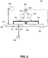
- FIG. 5 is a cross-sectional side view of the plasma deposition source 100 having three RF electrodes 301, according to further embodiments.
- Two adjacent RF electrodes 301 are connected by a connector 401, e.g. a power bracket, to each other such that adjacent RF electrodes 301 may be driven in phase if connected to an RF generator 400.
- the RF generator 400 provides an RF power output between a first generator pole 403 and a second generator pole 404.
- the second generator pole 404 is connected to ground or to a ground electrode.
- the ground or counter electrode corresponds to the substrate 500.
- the substrate 500 is electrically connected to the second generator pole 404, e.g. by electrically conducting rollers (not shown in FIG. 5 ).
- a ground or counter electrode might be provided in Fig. 5 below the substrate 500, i.e. such that a substrate receiving area is between the electrodes 301 and the ground or counter-electrode.
- a matching network 402 can be provided between the connectors 401 and the RF generator 400. The matching network 402 is provided for an impedance matching between the impedance of the RF arrangement of the RF electrodes 301 and the substrate 500, and the impedance of the RF generator 400.
- the RF generator 400 may provide a fixed frequency or may provide a frequency spectrum for exciting a plasma in the plasma volume 101.
- the RF frequency applied at the RF electrodes or at an individual RF electrode 301 may be in a range from 10 to 100 MHz, and typically amounts to about 40.68 MHz. Other typical driving frequencies are 13.56 MHz and 94.92 MHz.
- the plasma parameters provided in the plasma volume 101 such as plasma density, plasma pressure, plasma composition, decomposition of precursor gas, etc. may depend on the RF frequency, the electrode width 304 and the electrode-substrate gap distance 308.
- the RF generator 400 may be operated with a constant RF power density or the RF power density may be varied on the basis of the requirements for the deposition plasma and its parameters.
- the connectors 401 may be provided as power brackets for transferring the RF power density from the RF generator 400 via the matching network 402 to the connector 401. Furthermore, the RF generator 400 may provide frequencies depending on the electrode dimensions.
- the plasma deposition source 100 may be operated symmetrically, i.e. with the RF electrodes 301 connected in parallel by the connectors (power brackets) 401, from a single RF generator 400. Furthermore, the plasma deposition source 100 may alternatively be operated in a push-pull manner such that adjacent RF electrodes 301 are driven such that a phase difference of typically 180 degrees is provided between the adjacent RF electrodes 301.
- the RF electrodes 301 may be connected to each other by the connectors 401 and may be connected directly to the RF generator 400 by a further connection device. Furthermore, in accordance with some embodiments which may be combined with other embodiments described herein, the connector 401 may be used to connect each RF electrode 301 individually to the RF generator 400. Thus, at least one connector 401 is provided for electrically connecting the RF electrodes 301. Furthermore, according to yet another embodiment, which may be combined with other embodiments described herein, at least two connectors 401 may be provided for connecting the RF electrodes 301 to each other, wherein the at least two connectors 401 are arranged along the electrode length 305 being perpendicular to the substrate transport direction 501. Providing at least two connectors 401 along the length 305 of the RF electrode 301 may result in a more uniform plasma distribution in the plasma volume 101 along the length 305 of the RF electrode 301 perpendicular to the substrate transport direction 501.
- a gas supply device 200 is provided for supplying deposition gas such as silane to the gas inlet 201.
- a vacuum pump 606 is provided which is adapted for receiving gas output via the gas outlet 202.
- all gas inlets 201 may be connected to the same or different gas supply devices 200.
- all gas outlets 202 may be connected to the same or different vacuum pumps 606.
- a deposition gas flow across an RF electrode 301 from the gas inlet 201 to a gas outlet 202 may be controlled separately for each RF electrode 301.
- the operation of the gas supply device 200 in combination with the vacuum pump 606 may result in a typical pressure within the vacuum chamber which is in a range from 0.01 mbar to 10 mbar, typically is in a range from 0.01 mbar to 4.0 mbar, and more typically amounts to about 0.05 mbar. It is noted here that the pressure within the vacuum chamber may influence other plasma parameters such that an electrode-substrate gap distance 308 (see FIG. 2 ) may be changed in order to maintain a desired plasma deposition operation. A modification of the electrode-substrate gap distance 308, in turn, may influence e.g. the plasma volume 101 and the normalized plasma volume.
- deposition gases may be provided for each plasma volume 101 beneath an RF electrode 301.
- different deposition gases can be provided for different RF electrodes 301 such that complex deposition layer structures can be provided at the substrate surface 502.
- FIG. 6 is a detailed cross-sectional side view of a plasma deposition source 100 including three locally separated RF electrodes 301.
- Each RF electrode 301 has an RF input 405 for inputting RF power from an RF generator 400 (see FIG. 5 ).
- each RF electrode 301 includes an electrode isolation 306 for isolating the RF electrode 301 with respect to the environment.
- the two or more of the electrodes 301 can be connected to each other, e.g. with a connector, e.g. a power bracket.
- an electrode surface coating 307 protects each RF electrode 301 from plasma exposure.
- the surface coating of the electrodes can be provided as covers, for example made of glass or quartz.
- the covers can be removable, e.g. by clamping the covers on the electrodes. This allows for easy and fast replacement of the covers during maintenance of the thin film deposition system.
- a cover is adapted to be removably fixed to the electrode allowing replacement of low cost design covers.
- a high secondary electron emission coefficient of the electrode cover may provide a plasma stabilization at high pressures .
- FIG. 6 shows an input of the deposition gas through the gas inlet 201 and an output of the deposition gas through the gas outlet 202 separately for each electrode, in more detail.
- the gas inlet 201 is adapted to direct the deposition gas directly into the plasma volume 101, whereas the gas outlet 202 is provided at an upper rim of the plasma volume 101.
- the plasma volume is defined by the geometrical dimensions of the electrode and by the electrode-substrate gap distance 308, i.e. the plasma volume 101 is defined by the product of the electrode-substrate gap distance 308, the electrode width 304 and the electrode length 305 (see FIG. 1 ).
- the substrate 500 to be coated is located between the respective RF electrodes 301 and a counter-electrode 406.
- the counter-electrode 406 may be grounded, wherein the RF inputs 405 of the individual RF electrodes 301 are connected to the other pole of the RF generator 400 (see FIG. 5 ).
- the electrode arrangement shown in FIG. 6 has the advantage that the substrate 500 to be coated, which moves in the substrate transport direction 501, is not galvanically contacted for plasma generation purposes. Especially in the case of moving substrates 500, the arrangement shown in FIG. 6 may be used for deposition processes.
- the plasma deposition source 100 may be installed within a vacuum chamber in order to provide plasma deposition processes at reduced ambient pressure.
- the plasma deposition source 100 may be used for other plasma processes, such as, but not limited to, plasma etching processes, surface modification processes, plasma-enhanced surface activation, plasma-enhanced surface deactivation, etc..
- the electrodes may have a curved cross-sectional shape or may be arranged such that they rotate during a plasma deposition process.
- the RF electrodes 301 may be driven in phase or may be driven out of phase.
- Each RF electrode 301, with its respective gas inlet and gas outlets 201, 202 within the multi-region electrode device 300, may be operated separately.
- at least one different deposition gas may be fed into the plasma volume 101 provided by at least one RF electrode 301 with respect to the remaining RF electrodes 301.
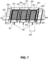
- FIG. 7 is a perspective view of the plasma deposition source 100, viewed at an observation angle from the bottom side where the substrate (not shown) is transported, in a substrate transport direction 501, past the RF electrodes 301.
- the RF electrodes 301 each have an electrode surface coating 307 for protecting the respective RF electrodes 301 from plasma exposure.
- the RF electrodes 301 each have gas lances at their edges perpendicular to the substrate transport direction 501, i.e. a respective gas inlet 201 and a respective gas outlet 202.
- the gas inlet 201 may have gas inlet openings 204 provided along the length of the gas inlet 201.
- Each RF electrode 301 of the multi-region electrode device 300 may be provided with RF power separately via RF inputs 405.
- the gas outlet 202 and, particularly the gas inlet 201 can be configurable or exchangeable.
- a gas distribution bar with opening 204 can be provided such that the gas distribution in the plasma region can be controlled.
- the gas distribution bar can have a symmetrical design with respect to the center line of the deposition source parallel to the substrate transport direction 501.
- the edge regions of the gas distribution bars with regard to the length directions of the electrodes might be provided with additional or larger openings 204 such that a loss of precursor gases at the edge of the electrode can be compensated for.
- the edge regions of the gas distribution bars with regard to the length directions of the electrodes might be provided with fewer or smaller openings 204 in order to reduce a buildup of deposition precursors and/or in order to further smooth the deposition profile.
- gas inlet openings 204 and/or gas outlet openings 205 may be provided in the form of slots.
- the respective slot may exhibit a varying slot width along the length of the slot, e.g. a larger or smaller slot width at the edge regions of the gas distribution bars.
- a gas pumping channel with opening 204 or a slit can be provided such that the evacuation from the plasma region can be controlled or adapted for uniform plasma behavior, i.e. uniform deposition over the substrate along the substrate direction perpendicular to the substrate moving direction.
- the gas pumping bar or gas pumping channel can have a symmetrical design with respect to the center line of the deposition source parallel to the substrate moving direction.
- the gas pumping channel can be configurable or exchangeable such that the existing differences in the length of the pumping channels are compensated for and a uniform flow resistance along the length of the gas outlet is provided.
- the multi-region electrode device 300 may be operated at driving RF frequencies in a range from 10 to 100 MHz, wherein typical frequencies are about 13.56 MHz to 94.92 MHz.
- the chosen driving RF frequency inter alia depends on the electrode dimensions.
- the multi-region electrode device 300 may be scaled up in dimension in order to provide a plasma enhanced-deposition of thin films onto larger substrates 500.
- a driving RF frequency may change in order to avoid a standing wave effect, which primarily affects the coating uniformity.
- Connectors 401 power brackets
- At least two connectors 401 may be arranged along the electrode length 305 which is perpendicular to the substrate transport direction 501.
- the electrode length 305 perpendicular to the substrate transport direction 501 may be in a range from 80 cm to 200 cm and typically in a range from 120 cm to 180 cm. According to another typical embodiment the electrode length 305 amounts to about 150 cm.
- the at least two connectors 401 provided along the electrode length 305 of an individual RF electrode 301 and which can be used for connecting the RF electrodes 301 to each other may be used to adjust an electric field uniformity and thus a plasma uniformity in the plasma volume (not shown in FIG. 7 ). Furthermore, by connecting the individual RF electrodes 301 separately to at lest one RF generator 400, a push-pull mode between two adjacent RF electrodes may be provided.
- a gas flow direction i.e. a gas flow from the gas inlet 201 to the gas outlet 202 across a RF electrode 301, is parallel to the substrate transport direction 501. Furthermore, it is possible that gas flow directions across two adj acent RF electrodes are aligned such that they are opposite to each other. Furthermore, according to yet another embodiment which can be combined with other embodiments described herein, a gas flow of the deposition gas may be adjusted such that the gas flow directions across all RF electrodes 301 are anti-parallel to the substrate transport direction 501.
- an electrode width 304 of the RF electrode 301 may be adjusted in relation to a depletion profile of the precursor gas such that a silane dust formation is reduced. Furthermore, deposition rates may be increased if the electrode width 304 is tuned with respect to the plasma parameters of the plasma provided in the plasma volume 101 and a depletion profile of the precursor gas. A further advantage is a more effective utilization of the deposition gas.
- the plasma deposition source 100 including the multi-region electrode device 300 may be used for deposition processes, as described herein above. Furthermore, according to yet further embodiments, the multi-region electrode device 300 may be designed for a use for etching and other surface modification processes such as, but not limited to, surface activation, surface passivation, etc.
- the deposition rate may be increased with a degree of activation of gas-phase precursors in a direct vicinity of the substrate surface 502 of the moving substrate 500.
- gas-phase precursors are controlled by a RF power density, the electrode-surface gap distance 308, a process gas flow 203 and a process gas composition.
- a formation of silane dust may be reduced on the basis of an adjustment of the electrode width 304 with respect to the depletion length of the precursor gas silane.
- a tuning of the electrode width 304 may thus effectively be provided to match a desired precursor depletion length profile.
- FIG. 8 is a flowchart illustrating a method for depositing a thin film onto a substrate.
- the method includes steps S1 to S7.
- the procedure starts at a step S1 and proceeds to a step S2 where a multi-region electrode device including at least two locally separated RF electrodes is provided.
- a substrate is guided past the RF electrodes in a substrate transport direction.
- Each of the at least two locally separated RF electrodes has a separate gas inlet and a separate gas outlet arranged at edges of the RF electrode which are perpendicular to the substrate transport direction.
- a deposition gas is guided from a respective gas inlet to a respective gas outlet of an individual RF electrode.
- RF power is supplied to the at least two RF electrodes.
- step S6 a thin film is deposited onto the guided substrate, which moves in the substrate transport direction.
- the procedure is ended at a step S7.
- a plasma deposition source adapted for transferring a deposition gas into a plasma phase and for depositing, from the plasma phase, a thin film onto a substrate moving in a substrate transport direction in a vacuum chamber.
- the plasma deposition source includes a multi-region electrode device adapted to be positioned in the vacuum chamber and including at least one RF electrode arranged opposite to the moving substrate and an RF power generator adapted for supplying RF power to the RF electrode.
- the RF electrode has at least one gas inlet arranged at one edge of the electrode and at least one gas outlet arranged at the opposed edge of the RF electrode.
- an electrode width of the RF electrode parallel to the substrate transport direction is less than the critical depletion length of the deposition gas, the critical depletion length being defined at a point at which the deposition gas mole fraction has dropped to a value of about 10% of its original value.
- the RF electrode defines a plasma volume between an electrode surface and an opposite substrate position within the vacuum chamber.
- a normalized plasma volume is provided by the plasma volume defined between the electrode surface and the opposite substrate position, divided by an electrode length, wherein the normalized plasma volume is provided on the basis of a deposition gas flow, a plasma pressure, the RF power and an RF frequency provided at the RF electrode.
- a gas supply device is provided which is adapted for supplying the deposition gas to the plasma volume.
- the at least one gas inlet is arranged at a leading edge of the RF electrode, and the at least one gas outlet is arranged at a trailing edge of the RF electrode, with respect to the substrate transport direction.
- the gas inlet and the gas outlet are arranged essentially perpendicular to the substrate transport direction.
- the plasma deposition source further includes at least one connector adapted for electrically connecting RF electrodes to each other.
- the plasma deposition source includes at least two connectors adapted for connecting RF electrodes to each other, wherein the at least two connectors are arranged along the electrode length being perpendicular to the substrate transport direction. At least two electrodes may be connected to a common generator pole. According to an optional modification, a matching network is provided for connecting the RF power generator to the multi-region electrode device. Furthermore, a counter-electrode may be arranged at a side of the moving substrate opposite to the at least RF electrode. According to a further modification, a RF frequency applied at the RF electrode is in a range from 10 to 100 MHz, and typically amounts to about 40.68 MHz.
- the electrode width is in a range from 10 cm to 18 cm, typically in a range from 12 cm to 17 cm, and more typically amounts to about 15 cm.
- the electrode length perpendicular to the substrate transport direction is in a range from 80 cm to 200 cm, typically in the range from 120 cm to 180 cm, and more typically amounts to about 150 cm.
- a method for depositing a thin film onto a substrate includes providing a multi-region electrode device including at least one RF electrode; guiding a substrate past the RF electrode in a substrate transport direction; flowing a deposition gas from a gas inlet to a gas outlet of RF electrode; supplying RF power to the RF electrode; and depositing the thin film onto the guide substrate.
- the method further may include controlling the deposition gas flow across the RF electrode from the gas inlet to the gas outlet separately for each RF electrode.
- the at least two RF electrodes are driven in phase.
- two adjacent electrodes are driven by a predetermined phase difference between each other.
- an electric field uniformity is adjusted by means of at least two connectors which are provided for connecting the RF electrodes to each other, along an electrode length being perpendicular to the substrate transport direction.
- an electrode-substrate gas distance is adjusted such that a depletion length of the deposition gas is equal to or larger than an electrode width parallel to the substrate transport direction.
- at least one different deposition gas is fed into the plasma volume provided by at least one RF electrode with respect to the remaining RF electrodes.
- the at least two RF electrodes are driven in a push-pull mode.
- An electrode width of the RF electrode is adjusted, according to yet another embodiment, such that a particle residence time is in a range from 0.01 s to 1 s, and typically amounts to about 0.4 s.
- a gas flow of the deposition gas is adjusted such that gas flow directions across two adjacent RF electrodes are opposite to each other.
- a gas flow of the deposition gas may be adjusted such that the gas flow directions across all RF electrodes are parallel or anti-parallel to the substrate transport direction.
Landscapes
- Chemical & Material Sciences (AREA)
- Engineering & Computer Science (AREA)
- Physics & Mathematics (AREA)
- Plasma & Fusion (AREA)
- Analytical Chemistry (AREA)
- Chemical Kinetics & Catalysis (AREA)
- Materials Engineering (AREA)
- Mechanical Engineering (AREA)
- Metallurgy (AREA)
- Organic Chemistry (AREA)
- Chemical Vapour Deposition (AREA)
- Plasma Technology (AREA)
Priority Applications (7)
| Application Number | Priority Date | Filing Date | Title |
|---|---|---|---|
| EP09161034.5A EP2256782B1 (en) | 2009-05-25 | 2009-05-25 | Plasma deposition source and method for depositing thin films |
| US12/476,891 US20100297361A1 (en) | 2009-05-25 | 2009-06-02 | Plasma deposition source and method for depositing thin films |
| TW099116533A TWI590715B (zh) | 2009-05-25 | 2010-05-24 | 電漿沉積源及用以沉積薄膜之方法 |
| KR1020117030911A KR101698446B1 (ko) | 2009-05-25 | 2010-05-25 | 플라즈마 증착 소스 및 박막들을 증착하기 위한 방법 |
| PCT/EP2010/057181 WO2010136464A1 (en) | 2009-05-25 | 2010-05-25 | Plasma deposition source and method for depositing thin films |
| JP2012511305A JP5659225B2 (ja) | 2009-05-25 | 2010-05-25 | プラズマ堆積ソースおよび薄膜を堆積させるための方法 |
| CN201080023248.XA CN102449726B (zh) | 2009-05-25 | 2010-05-25 | 等离子体沉积源和用于沉积薄膜的方法 |
Applications Claiming Priority (1)
| Application Number | Priority Date | Filing Date | Title |
|---|---|---|---|
| EP09161034.5A EP2256782B1 (en) | 2009-05-25 | 2009-05-25 | Plasma deposition source and method for depositing thin films |
Publications (2)
| Publication Number | Publication Date |
|---|---|
| EP2256782A1 EP2256782A1 (en) | 2010-12-01 |
| EP2256782B1 true EP2256782B1 (en) | 2018-08-29 |
Family
ID=41110602
Family Applications (1)
| Application Number | Title | Priority Date | Filing Date |
|---|---|---|---|
| EP09161034.5A Not-in-force EP2256782B1 (en) | 2009-05-25 | 2009-05-25 | Plasma deposition source and method for depositing thin films |
Country Status (7)
Families Citing this family (8)
| Publication number | Priority date | Publication date | Assignee | Title |
|---|---|---|---|---|
| EP2915902B1 (en) * | 2012-11-02 | 2020-02-19 | AGC Inc. | Plasma source for a plasma cvd apparatus and a manufacturing method of an article using the plasma source |
| KR101464939B1 (ko) * | 2013-02-21 | 2014-11-25 | 주식회사 테스 | 박막증착장치 |
| US9738976B2 (en) * | 2013-02-27 | 2017-08-22 | Ioxus, Inc. | Energy storage device assembly |
| KR102244070B1 (ko) * | 2014-01-07 | 2021-04-26 | 삼성디스플레이 주식회사 | 기상 증착 장치, 기상 증착 방법 및 유기 발광 표시 장치 제조 방법 |
| CN109659217A (zh) * | 2018-12-18 | 2019-04-19 | 沈阳拓荆科技有限公司 | 用于多等离子处理腔的射频系统 |
| WO2020257965A1 (en) * | 2019-06-24 | 2020-12-30 | Trumpf Huettinger (Shanghai) Co., Ltd. | Method of adjusting the output power of a power supply supplying electrical power to a plasma, plasma apparatus and power supply |
| EP3761341A1 (en) * | 2019-07-03 | 2021-01-06 | Nederlandse Organisatie voor toegepast- natuurwetenschappelijk Onderzoek TNO | Spatially controlled plasma delivery apparatus |
| CN114836736A (zh) * | 2021-02-01 | 2022-08-02 | 江苏菲沃泰纳米科技股份有限公司 | 等离子体镀膜设备和镀膜方法 |
Citations (1)
| Publication number | Priority date | Publication date | Assignee | Title |
|---|---|---|---|---|
| US20080096305A1 (en) * | 2006-10-23 | 2008-04-24 | Canon Kabushiki Kaisha | Method for forming deposited film and photovoltaic element |
Family Cites Families (10)
| Publication number | Priority date | Publication date | Assignee | Title |
|---|---|---|---|---|
| JPH06101459B2 (ja) * | 1985-05-09 | 1994-12-12 | 松下電器産業株式会社 | プラズマ気相成長装置 |
| US5180434A (en) * | 1991-03-11 | 1993-01-19 | United Solar Systems Corporation | Interfacial plasma bars for photovoltaic deposition apparatus |
| US6022414A (en) * | 1994-07-18 | 2000-02-08 | Semiconductor Equipment Group, Llc | Single body injector and method for delivering gases to a surface |
| JPH0867986A (ja) * | 1994-08-29 | 1996-03-12 | Canon Inc | 大面積機能性堆積膜の連続的形成方法及び形成装置 |
| WO1997022136A1 (de) * | 1995-12-08 | 1997-06-19 | Balzers Aktiengesellschaft | Hf-plasmabehandlungskammer bzw. pecvd-beschichtungskammer, deren verwendungen und verfahren zur beschichtung von speicherplatten |
| JPH11246971A (ja) | 1998-03-03 | 1999-09-14 | Canon Inc | 微結晶シリコン系薄膜の作製方法及び作製装置 |
| JP3332857B2 (ja) * | 1998-04-15 | 2002-10-07 | 三菱重工業株式会社 | 高周波プラズマ発生装置及び給電方法 |
| JP2001049440A (ja) * | 1999-08-13 | 2001-02-20 | Mitsubishi Heavy Ind Ltd | プラズマcvd製膜方法及びプラズマcvd製膜装置 |
| US6849306B2 (en) * | 2001-08-23 | 2005-02-01 | Konica Corporation | Plasma treatment method at atmospheric pressure |
| US20070154650A1 (en) * | 2005-12-30 | 2007-07-05 | Atomic Energy Council - Institute Of Nuclear Energy Research | Method and apparatus for glow discharge plasma treatment of flexible material at atmospheric pressure |
-
2009
- 2009-05-25 EP EP09161034.5A patent/EP2256782B1/en not_active Not-in-force
- 2009-06-02 US US12/476,891 patent/US20100297361A1/en not_active Abandoned
-
2010
- 2010-05-24 TW TW099116533A patent/TWI590715B/zh not_active IP Right Cessation
- 2010-05-25 WO PCT/EP2010/057181 patent/WO2010136464A1/en active Application Filing
- 2010-05-25 CN CN201080023248.XA patent/CN102449726B/zh not_active Expired - Fee Related
- 2010-05-25 JP JP2012511305A patent/JP5659225B2/ja not_active Expired - Fee Related
- 2010-05-25 KR KR1020117030911A patent/KR101698446B1/ko not_active Expired - Fee Related
Patent Citations (1)
| Publication number | Priority date | Publication date | Assignee | Title |
|---|---|---|---|---|
| US20080096305A1 (en) * | 2006-10-23 | 2008-04-24 | Canon Kabushiki Kaisha | Method for forming deposited film and photovoltaic element |
Non-Patent Citations (1)
| Title |
|---|
| BUGNON G ET AL: "Influence of pressure and silane depletion on microcrystalline silicon material quality and solar cell performance", JOURNAL OF APPLIED PHYSICS, AMERICAN INSTITUTE OF PHYSICS, US, vol. 105, no. 6, 20 March 2009 (2009-03-20), pages 64507 - 64507, XP012120211, ISSN: 0021-8979, DOI: 10.1063/1.3095488 * |
Also Published As
| Publication number | Publication date |
|---|---|
| TWI590715B (zh) | 2017-07-01 |
| CN102449726A (zh) | 2012-05-09 |
| JP2012528242A (ja) | 2012-11-12 |
| EP2256782A1 (en) | 2010-12-01 |
| WO2010136464A1 (en) | 2010-12-02 |
| TW201106807A (en) | 2011-02-16 |
| JP5659225B2 (ja) | 2015-01-28 |
| KR101698446B1 (ko) | 2017-01-20 |
| CN102449726B (zh) | 2016-08-03 |
| US20100297361A1 (en) | 2010-11-25 |
| KR20120030453A (ko) | 2012-03-28 |
Similar Documents
| Publication | Publication Date | Title |
|---|---|---|
| EP2256782B1 (en) | Plasma deposition source and method for depositing thin films | |
| US9359674B2 (en) | Apparatus and method for dielectric deposition | |
| US20140212601A1 (en) | Methods for plasma processing | |
| US20100144122A1 (en) | Hybrid chemical vapor deposition process combining hot-wire cvd and plasma-enhanced cvd | |
| CA2709717A1 (en) | Plasma enhanced chemical vapor deposition of barrier coatings | |
| JP5378416B2 (ja) | プラズマ処理装置 | |
| JP4408821B2 (ja) | プラズマ処理装置 | |
| JP2012043983A (ja) | 多層膜形成方法およびそれに用いる成膜装置 | |
| JP2007266094A (ja) | プラズマcvd装置及びプラズマcvdによる半導体薄膜の成膜方法 | |
| JP4273382B2 (ja) | プラズマ処理装置と薄膜形成方法 | |
| EP2471973A1 (en) | Apparatus for forming deposited film and method for forming deposited film | |
| JP2011155308A (ja) | プラズマcvd装置及びプラズマcvd装置を用いたシリコン系膜の製造方法 | |
| JP2012507133A (ja) | 基板上にプロセシングされる材料の均一性を改善する堆積装置及びこれを使用する方法 | |
| JP2009302572A (ja) | プラズマ処理装置 | |
| JP2006100551A (ja) | プラズマ製膜方法、プラズマ処理装置、太陽電池及び太陽電池の製造方法 | |
| WO2013031142A1 (ja) | 成膜方法及び記憶媒体 | |
| WO2019227192A1 (ru) | Технологический реактор для плазмохимического осаждения тонкопленочных покрытий и вакуумная установка | |
| CN114293174A (zh) | 气体供应单元和包括气体供应单元的衬底处理设备 | |
| KR20070053317A (ko) | 플라즈마 강화 화학 기상 성장 장치 및 방법 | |
| JPH0272677A (ja) | 薄膜半導体の製造装置 | |
| JP2010103564A (ja) | プラズマ処理装置 | |
| JP2010287898A (ja) | プラズマ製膜方法及び太陽電池の製造方法 | |
| JP2010232684A (ja) | プラズマ処理装置 |
Legal Events
| Date | Code | Title | Description |
|---|---|---|---|
| PUAI | Public reference made under article 153(3) epc to a published international application that has entered the european phase |
Free format text: ORIGINAL CODE: 0009012 |
|
| AK | Designated contracting states |
Kind code of ref document: A1 Designated state(s): AT BE BG CH CY CZ DE DK EE ES FI FR GB GR HR HU IE IS IT LI LT LU LV MC MK MT NL NO PL PT RO SE SI SK TR |
|
| 17P | Request for examination filed |
Effective date: 20110601 |
|
| STAA | Information on the status of an ep patent application or granted ep patent |
Free format text: STATUS: EXAMINATION IS IN PROGRESS |
|
| 17Q | First examination report despatched |
Effective date: 20161130 |
|
| GRAP | Despatch of communication of intention to grant a patent |
Free format text: ORIGINAL CODE: EPIDOSNIGR1 |
|
| STAA | Information on the status of an ep patent application or granted ep patent |
Free format text: STATUS: GRANT OF PATENT IS INTENDED |
|
| INTG | Intention to grant announced |
Effective date: 20180312 |
|
| GRAS | Grant fee paid |
Free format text: ORIGINAL CODE: EPIDOSNIGR3 |
|
| GRAA | (expected) grant |
Free format text: ORIGINAL CODE: 0009210 |
|
| STAA | Information on the status of an ep patent application or granted ep patent |
Free format text: STATUS: THE PATENT HAS BEEN GRANTED |
|
| AK | Designated contracting states |
Kind code of ref document: B1 Designated state(s): AT BE BG CH CY CZ DE DK EE ES FI FR GB GR HR HU IE IS IT LI LT LU LV MC MK MT NL NO PL PT RO SE SI SK TR |
|
| REG | Reference to a national code |
Ref country code: GB Ref legal event code: FG4D |
|
| REG | Reference to a national code |
Ref country code: CH Ref legal event code: EP |
|
| REG | Reference to a national code |
Ref country code: AT Ref legal event code: REF Ref document number: 1036140 Country of ref document: AT Kind code of ref document: T Effective date: 20180915 |
|
| REG | Reference to a national code |
Ref country code: IE Ref legal event code: FG4D |
|
| REG | Reference to a national code |
Ref country code: DE Ref legal event code: R096 Ref document number: 602009054122 Country of ref document: DE |
|
| REG | Reference to a national code |
Ref country code: CH Ref legal event code: NV Representative=s name: MICHELI AND CIE SA, CH |
|
| REG | Reference to a national code |
Ref country code: NL Ref legal event code: MP Effective date: 20180829 |
|
| REG | Reference to a national code |
Ref country code: LT Ref legal event code: MG4D |
|
| PG25 | Lapsed in a contracting state [announced via postgrant information from national office to epo] |
Ref country code: NL Free format text: LAPSE BECAUSE OF FAILURE TO SUBMIT A TRANSLATION OF THE DESCRIPTION OR TO PAY THE FEE WITHIN THE PRESCRIBED TIME-LIMIT Effective date: 20180829 Ref country code: SE Free format text: LAPSE BECAUSE OF FAILURE TO SUBMIT A TRANSLATION OF THE DESCRIPTION OR TO PAY THE FEE WITHIN THE PRESCRIBED TIME-LIMIT Effective date: 20180829 Ref country code: LT Free format text: LAPSE BECAUSE OF FAILURE TO SUBMIT A TRANSLATION OF THE DESCRIPTION OR TO PAY THE FEE WITHIN THE PRESCRIBED TIME-LIMIT Effective date: 20180829 Ref country code: BG Free format text: LAPSE BECAUSE OF FAILURE TO SUBMIT A TRANSLATION OF THE DESCRIPTION OR TO PAY THE FEE WITHIN THE PRESCRIBED TIME-LIMIT Effective date: 20181129 Ref country code: NO Free format text: LAPSE BECAUSE OF FAILURE TO SUBMIT A TRANSLATION OF THE DESCRIPTION OR TO PAY THE FEE WITHIN THE PRESCRIBED TIME-LIMIT Effective date: 20181129 Ref country code: IS Free format text: LAPSE BECAUSE OF FAILURE TO SUBMIT A TRANSLATION OF THE DESCRIPTION OR TO PAY THE FEE WITHIN THE PRESCRIBED TIME-LIMIT Effective date: 20181229 Ref country code: FI Free format text: LAPSE BECAUSE OF FAILURE TO SUBMIT A TRANSLATION OF THE DESCRIPTION OR TO PAY THE FEE WITHIN THE PRESCRIBED TIME-LIMIT Effective date: 20180829 Ref country code: GR Free format text: LAPSE BECAUSE OF FAILURE TO SUBMIT A TRANSLATION OF THE DESCRIPTION OR TO PAY THE FEE WITHIN THE PRESCRIBED TIME-LIMIT Effective date: 20181130 |
|
| REG | Reference to a national code |
Ref country code: AT Ref legal event code: MK05 Ref document number: 1036140 Country of ref document: AT Kind code of ref document: T Effective date: 20180829 |
|
| PG25 | Lapsed in a contracting state [announced via postgrant information from national office to epo] |
Ref country code: LV Free format text: LAPSE BECAUSE OF FAILURE TO SUBMIT A TRANSLATION OF THE DESCRIPTION OR TO PAY THE FEE WITHIN THE PRESCRIBED TIME-LIMIT Effective date: 20180829 Ref country code: HR Free format text: LAPSE BECAUSE OF FAILURE TO SUBMIT A TRANSLATION OF THE DESCRIPTION OR TO PAY THE FEE WITHIN THE PRESCRIBED TIME-LIMIT Effective date: 20180829 Ref country code: ES Free format text: LAPSE BECAUSE OF FAILURE TO SUBMIT A TRANSLATION OF THE DESCRIPTION OR TO PAY THE FEE WITHIN THE PRESCRIBED TIME-LIMIT Effective date: 20180829 |
|
| PG25 | Lapsed in a contracting state [announced via postgrant information from national office to epo] |
Ref country code: IT Free format text: LAPSE BECAUSE OF FAILURE TO SUBMIT A TRANSLATION OF THE DESCRIPTION OR TO PAY THE FEE WITHIN THE PRESCRIBED TIME-LIMIT Effective date: 20180829 Ref country code: RO Free format text: LAPSE BECAUSE OF FAILURE TO SUBMIT A TRANSLATION OF THE DESCRIPTION OR TO PAY THE FEE WITHIN THE PRESCRIBED TIME-LIMIT Effective date: 20180829 Ref country code: CZ Free format text: LAPSE BECAUSE OF FAILURE TO SUBMIT A TRANSLATION OF THE DESCRIPTION OR TO PAY THE FEE WITHIN THE PRESCRIBED TIME-LIMIT Effective date: 20180829 Ref country code: PL Free format text: LAPSE BECAUSE OF FAILURE TO SUBMIT A TRANSLATION OF THE DESCRIPTION OR TO PAY THE FEE WITHIN THE PRESCRIBED TIME-LIMIT Effective date: 20180829 Ref country code: EE Free format text: LAPSE BECAUSE OF FAILURE TO SUBMIT A TRANSLATION OF THE DESCRIPTION OR TO PAY THE FEE WITHIN THE PRESCRIBED TIME-LIMIT Effective date: 20180829 Ref country code: AT Free format text: LAPSE BECAUSE OF FAILURE TO SUBMIT A TRANSLATION OF THE DESCRIPTION OR TO PAY THE FEE WITHIN THE PRESCRIBED TIME-LIMIT Effective date: 20180829 |
|
| PG25 | Lapsed in a contracting state [announced via postgrant information from national office to epo] |
Ref country code: DK Free format text: LAPSE BECAUSE OF FAILURE TO SUBMIT A TRANSLATION OF THE DESCRIPTION OR TO PAY THE FEE WITHIN THE PRESCRIBED TIME-LIMIT Effective date: 20180829 Ref country code: SK Free format text: LAPSE BECAUSE OF FAILURE TO SUBMIT A TRANSLATION OF THE DESCRIPTION OR TO PAY THE FEE WITHIN THE PRESCRIBED TIME-LIMIT Effective date: 20180829 |
|
| REG | Reference to a national code |
Ref country code: DE Ref legal event code: R097 Ref document number: 602009054122 Country of ref document: DE |
|
| PLBE | No opposition filed within time limit |
Free format text: ORIGINAL CODE: 0009261 |
|
| STAA | Information on the status of an ep patent application or granted ep patent |
Free format text: STATUS: NO OPPOSITION FILED WITHIN TIME LIMIT |
|
| PGFP | Annual fee paid to national office [announced via postgrant information from national office to epo] |
Ref country code: DE Payment date: 20190521 Year of fee payment: 11 |
|
| 26N | No opposition filed |
Effective date: 20190531 |
|
| PG25 | Lapsed in a contracting state [announced via postgrant information from national office to epo] |
Ref country code: SI Free format text: LAPSE BECAUSE OF FAILURE TO SUBMIT A TRANSLATION OF THE DESCRIPTION OR TO PAY THE FEE WITHIN THE PRESCRIBED TIME-LIMIT Effective date: 20180829 |
|
| PGFP | Annual fee paid to national office [announced via postgrant information from national office to epo] |
Ref country code: CH Payment date: 20190521 Year of fee payment: 11 |
|
| PGFP | Annual fee paid to national office [announced via postgrant information from national office to epo] |
Ref country code: GB Payment date: 20190521 Year of fee payment: 11 |
|
| PG25 | Lapsed in a contracting state [announced via postgrant information from national office to epo] |
Ref country code: MC Free format text: LAPSE BECAUSE OF FAILURE TO SUBMIT A TRANSLATION OF THE DESCRIPTION OR TO PAY THE FEE WITHIN THE PRESCRIBED TIME-LIMIT Effective date: 20180829 |
|
| REG | Reference to a national code |
Ref country code: BE Ref legal event code: MM Effective date: 20190531 |
|
| PG25 | Lapsed in a contracting state [announced via postgrant information from national office to epo] |
Ref country code: LU Free format text: LAPSE BECAUSE OF NON-PAYMENT OF DUE FEES Effective date: 20190525 |
|
| PG25 | Lapsed in a contracting state [announced via postgrant information from national office to epo] |
Ref country code: TR Free format text: LAPSE BECAUSE OF FAILURE TO SUBMIT A TRANSLATION OF THE DESCRIPTION OR TO PAY THE FEE WITHIN THE PRESCRIBED TIME-LIMIT Effective date: 20180829 |
|
| PG25 | Lapsed in a contracting state [announced via postgrant information from national office to epo] |
Ref country code: IE Free format text: LAPSE BECAUSE OF NON-PAYMENT OF DUE FEES Effective date: 20190525 |
|
| PG25 | Lapsed in a contracting state [announced via postgrant information from national office to epo] |
Ref country code: BE Free format text: LAPSE BECAUSE OF NON-PAYMENT OF DUE FEES Effective date: 20190531 |
|
| PG25 | Lapsed in a contracting state [announced via postgrant information from national office to epo] |
Ref country code: PT Free format text: LAPSE BECAUSE OF FAILURE TO SUBMIT A TRANSLATION OF THE DESCRIPTION OR TO PAY THE FEE WITHIN THE PRESCRIBED TIME-LIMIT Effective date: 20181229 Ref country code: FR Free format text: LAPSE BECAUSE OF NON-PAYMENT OF DUE FEES Effective date: 20190531 |
|
| REG | Reference to a national code |
Ref country code: DE Ref legal event code: R119 Ref document number: 602009054122 Country of ref document: DE |
|
| PG25 | Lapsed in a contracting state [announced via postgrant information from national office to epo] |
Ref country code: LI Free format text: LAPSE BECAUSE OF NON-PAYMENT OF DUE FEES Effective date: 20200531 Ref country code: CH Free format text: LAPSE BECAUSE OF NON-PAYMENT OF DUE FEES Effective date: 20200531 |
|
| GBPC | Gb: european patent ceased through non-payment of renewal fee |
Effective date: 20200525 |
|
| PG25 | Lapsed in a contracting state [announced via postgrant information from national office to epo] |
Ref country code: GB Free format text: LAPSE BECAUSE OF NON-PAYMENT OF DUE FEES Effective date: 20200525 |
|
| PG25 | Lapsed in a contracting state [announced via postgrant information from national office to epo] |
Ref country code: DE Free format text: LAPSE BECAUSE OF NON-PAYMENT OF DUE FEES Effective date: 20201201 Ref country code: CY Free format text: LAPSE BECAUSE OF FAILURE TO SUBMIT A TRANSLATION OF THE DESCRIPTION OR TO PAY THE FEE WITHIN THE PRESCRIBED TIME-LIMIT Effective date: 20180829 |
|
| PG25 | Lapsed in a contracting state [announced via postgrant information from national office to epo] |
Ref country code: HU Free format text: LAPSE BECAUSE OF FAILURE TO SUBMIT A TRANSLATION OF THE DESCRIPTION OR TO PAY THE FEE WITHIN THE PRESCRIBED TIME-LIMIT; INVALID AB INITIO Effective date: 20090525 Ref country code: MT Free format text: LAPSE BECAUSE OF FAILURE TO SUBMIT A TRANSLATION OF THE DESCRIPTION OR TO PAY THE FEE WITHIN THE PRESCRIBED TIME-LIMIT Effective date: 20180829 |
|
| PG25 | Lapsed in a contracting state [announced via postgrant information from national office to epo] |
Ref country code: MK Free format text: LAPSE BECAUSE OF FAILURE TO SUBMIT A TRANSLATION OF THE DESCRIPTION OR TO PAY THE FEE WITHIN THE PRESCRIBED TIME-LIMIT Effective date: 20180829 |