EP2255447B1 - Automatische filtersteuerung - Google Patents
Automatische filtersteuerung Download PDFInfo
- Publication number
- EP2255447B1 EP2255447B1 EP09723830.7A EP09723830A EP2255447B1 EP 2255447 B1 EP2255447 B1 EP 2255447B1 EP 09723830 A EP09723830 A EP 09723830A EP 2255447 B1 EP2255447 B1 EP 2255447B1
- Authority
- EP
- European Patent Office
- Prior art keywords
- power
- filter
- band
- signal
- controlling
- Prior art date
- Legal status (The legal status is an assumption and is not a legal conclusion. Google has not performed a legal analysis and makes no representation as to the accuracy of the status listed.)
- Active
Links
Images




Classifications
-
- H—ELECTRICITY
- H04—ELECTRIC COMMUNICATION TECHNIQUE
- H04W—WIRELESS COMMUNICATION NETWORKS
- H04W52/00—Power management, e.g. Transmission Power Control [TPC] or power classes
- H04W52/02—Power saving arrangements
- H04W52/0209—Power saving arrangements in terminal devices
- H04W52/0225—Power saving arrangements in terminal devices using monitoring of external events, e.g. the presence of a signal
-
- Y—GENERAL TAGGING OF NEW TECHNOLOGICAL DEVELOPMENTS; GENERAL TAGGING OF CROSS-SECTIONAL TECHNOLOGIES SPANNING OVER SEVERAL SECTIONS OF THE IPC; TECHNICAL SUBJECTS COVERED BY FORMER USPC CROSS-REFERENCE ART COLLECTIONS [XRACs] AND DIGESTS
- Y02—TECHNOLOGIES OR APPLICATIONS FOR MITIGATION OR ADAPTATION AGAINST CLIMATE CHANGE
- Y02D—CLIMATE CHANGE MITIGATION TECHNOLOGIES IN INFORMATION AND COMMUNICATION TECHNOLOGIES [ICT], I.E. INFORMATION AND COMMUNICATION TECHNOLOGIES AIMING AT THE REDUCTION OF THEIR OWN ENERGY USE
- Y02D30/00—Reducing energy consumption in communication networks
- Y02D30/70—Reducing energy consumption in communication networks in wireless communication networks
Definitions
- the present invention relates generally to wireless receivers, and more particularly to controlling power consumption of a wireless receiver based on performance requirements and current operating conditions.
- Wireless receivers are designed to receive and process wireless signals so that the receiver meets the performance requirements, e.g., bit error rate, data rate, etc., defined by a controlling communication standard and associated with a known range of operating conditions.
- the receiver may be designed to accommodate the worst-case operating condition to ensure that the performance requirements are met for all operating conditions.
- the receiver may be designed to meet a bit error rate requirement under a worst-case operating condition, i.e., when an out-of-band blocking signal strongly interferes with an in-band desired signal. Because worst-case operating conditions rarely occur, a receiver with a fixed design wastes power when the operating condition is better than the worst case.
- a wireless receiver may have a dynamic design (e.g., may be designed with dynamically adjustable parameters).
- U.S. Patent No. 7,010,330 describes dynamically modifying the gain, bias points, or impedance level of a circuit element in a receiver depending on the quality of a received signal. For example, if the received signal has good quality, the receiver gain may be reduced to reduce the overall power consumption of the receiver. If the received signal has poor signal quality, the receiver gain may be increased to provide the desired performance at the expense of higher power consumption.
- WO 2007/134201 A2 describes techniques for controlling operation of control loops in a receiver.
- the operation of at least one control loop is modified in conjunction with a change in operating state, which may correspond to a change in linearity state, gain state, operating frequency, antenna configuration, etc.
- a change in linearity state may occur when jammers are detected and may cause bias current of analog circuit blocks to be adjusted.
- the at least one control loop to be modified may include a DC loop, an AGC loop, etc.
- the operation of a control loop may be modified by disabling the control loop or changing its time constant prior to changing operating state, waiting a predetermined amount of time to allow the receiver to settle, and enabling the control loop or restoring its time constant after waiting the predetermined amount of time.
- US 2008/039047 A1 discloses a reception system that includes a detection circuit serving as detecting means for detecting that the strength of the receiver signal is equal to or greater than a predetermined value, and a resetting circuit serving as resetting means for, under instruction of the detection circuit, immediately increasing power consumption of the reception section when the detection circuit detects a large signal so as to bring back the state where the reception system ensures the greatest power consumption amount for the entire system and the sufficiently-desirable system performance.
- US 7,010,330 B1 discloses methods and circuits for reducing power dissipation in wireless transceivers and other electronic circuits and systems. Bias current reduction, impedance scaling, and gain changes are used, either separately or in combination, to reduce power dissipation. For example, bias currents are reduced in response to a need for reduced signal handling capability, impedances are scaled thus reducing required drive and other bias currents in response to a strong received signal, or gain is increased and impedances are scaled in response to a low received signal in the presence of no or weak interfering signals.
- the present invention provides an alternate solution for controlling the power consumption of a receiver based on current operating conditions.
- a receiver receives a signal and applies the received signal to a variable filter.
- the received signal includes a desired in-band signal.
- the received signal may further include one or more unwanted out-of-band signals, referred to herein as blocking signals.
- the present invention controls one or more parameters of the variable filter to maintain a current ratio at the filter output between one or more blocking signal power levels and a desired signal power level such that the current ratio satisfies a predetermined criteria relative to a desired ratio level.
- the present invention may control one or more parameters of the variable filter to maintain a current ratio at the filter output of the one or more blocking signal power levels to the desired signal power level at or below the desired ratio level. In so doing, the present invention limits the receiver power consumption while still providing the desired receiver performance.
- a wireless receiver comprises a variable filter, a power measurement element, and a controller.
- the variable filter filters a received signal.
- the power measurement element measures a total power and an in-band power of the filtered signal.
- the controller compares the total power with the in-band power, and controls one or more operating parameters of the variable filter based on the comparison to achieve a desired receiver performance while minimizing the receiver power consumption.
- the controller may compare the total and in-band powers by subtracting the total and in-band powers.
- the controller may compare the total and in-band powers by determining a ratio between the total and in-band powers.
- the controller may increase the out-of-band attenuation of the filter relative to the passband to further filter the blocking signal(s), and therefore, to provide the desired ratio between the blocking and desired signals.
- the controller provides the required receiver performance at the expense of an increase in receiver power consumption.
- the controller may decrease the out-of-band attenuation. Such a decrease reduces the receiver power consumption without adversely affecting the receiver performance.
- Wireless receivers are designed to receive and process wireless signals so that the receiver meets predetermined performance requirements, e.g., bit error rate, data rate, etc. defined by a controlling communication standard. Because the receiver performance may change as the operating conditions change, the receiver must further be designed to accommodate a variety of operating conditions. Fixed wireless receiver designs are typically configured for worst-case operating conditions. Because such worst-case operating conditions are rare, wireless receivers having a fixed design typically consume unnecessarily large amounts of power.
- the present invention provides a dynamic receiver design that controls receiver performance by controlling parameters of a variable filter applied to a received signal based on current operating conditions that impact the strength and presence of out-of-band blocking signals in the received signal.
- the filter passes the in-band signal and attenuates the blocking signals according to a filter transfer function. Whenever the blocking signals have a sufficiently low power level relative to the desired in-band signal, the out-of-band attenuation of the filter may be decreased to save power.
- the present invention provides a receiver that achieves a desired performance without consuming unnecessary power.
- FIG. 1 shows an exemplary receiver 10 according to one embodiment of the present invention.
- Receiver 10 comprises an antenna 12, receiver front-end 13, variable filter 14, optional amplifier 16, analog-to-digital converter (ADC) 18, digital processor 20, and filter controller 22.
- the receiver front-end 13 comprises amplifiers, mixers, etc. to process the signal received by antenna 12 according to any known means to generate an input signal S IN .
- Filter 14 filters S IN according to a current filter transfer function to generate a filtered signal S OUT .
- amplifier 16 amplifies the filtered signal S OUT a desired amount to reduce dynamic range requirements for the ADC 18. It will be appreciated that the amplifier 16 does not affect the filter control of the present invention.
- ADC 18 converts the filtered signal S OUT to a digital signal according to any known means.
- ADC 18 may comprise any type of ADC, e.g., a delta-sigma ADC, a direct conversion ADC (e.g., a flash ADC), a successive approximation ADC, etc.
- Processor 20 comprises any known digital processing circuit that digitally processes the received signal to generate the receiver output signal.
- Exemplary processors 20 may be implemented in a single processor or in multiple processors and include, but are not limited to, general purpose and/or special purpose microprocessors and digital signal processors.
- the processor 20 further measures the total power P out and the in-band power P s of the filtered signal S OUT , and provides the results to filter controller 22.
- Filter controller 22 generates one or more control signals U to control one or more operating parameters of the filter 14 based on a comparison between the provided signal powers P out , P s .
- the control signal U may control an order of the filter, a passband gain of the filter, and/or a filter transfer function.
- Control signal U may comprise an analog and/or digital signal, depending on the implementation of the filter 14, that controls the filter 14 either continuously or in discrete steps.
- Figure 2 shows an example of the effect of filter 14 on the input signal S IN .
- filter 14 filters the input signal S IN based on current filter operating parameters to pass the desired in-band signal at frequency f s and to attenuate the blocking signal(s) at frequency f b .
- filter 14 controls the power ratio between the in-band signal power P s and the blocking signal power P b .
- the present invention seeks to maintain a desired power ratio ⁇ r between the blocking signal power P b and the in-band signal power P s of the filtered output signal S OUT such that the desired power ratio satisfies a predetermined criteria relative to a desired value.
- the present invention seeks to maintain the power ratio ⁇ r at or below the desired value.
- controlling the operating parameters of the filter 14, e.g., the passband gain, the filter transfer function, the order of the filter, etc. controls the power ratio ⁇ r achieved by the filter 14.
- the following describes the invention in terms of the power ratio defined by Equation (3).
- the power ratio ⁇ r may alternatively be expressed as a function of the ratio of the in-band signal power P s to the blocking signal power P b , where the present invention would maintain such a ratio at or above the desired value.
- processor 20 may measure the power P s of the in-band signal according to any known means. Further, the processor 20 may measure the total power P OUT of the filtered signal S OUT . However, the power of the blocking signal(s) P b is not as easily obtained. To overcome this problem, Equation (2) may be rearranged and substituted into Equation (3) to define the ratio ⁇ r in terms of the in-band signal power P s and the total output power P OUT , as given by Equation (4).
- Equation (2) may be rearranged and substituted into Equation (3) to define the ratio ⁇ r in terms of the in-band signal power P s and the total output power P OUT , as given by Equation (4).
- ⁇ r may be expressed in terms of a power differential based on a ratio between the total output power P OUT and the in-band signal power P s (e.g., when P s and P OUT are expressed in terms of a linear power scale), as shown by Equation (4). It will be appreciated that while Equation (4) expresses ⁇ r as a function of the ratio of P OUT to P s , ⁇ r may alternatively be expressed as a function of the ratio of P s to P OUT .
- ⁇ r may be expressed as a function of a power differential computed based on a difference between the total output power P OUT and the in-band signal power P s , e.g., as a function of P OUT - P s .
- processor 20 may determine and provide the in-band signal power P s and the total output power P OUT to the filter controller 22 to support the filter control process of the present invention.
- FIG 3 shows one exemplary digital processor 20 for the receiver 10 of Figure 1 .
- Processor 20 includes received signal processing elements 24, decimator 26, channel selection filter 28, and digital power detectors 30.
- Decimator 26 reduces the sampling rate of the input digital signal and provides the decimated signal to the digital power detector 30 and to the channel selection filter 28.
- the channel selection filter 28 comprises a sharp filter that filters the decimated signal to obtain the desired in-band signal.
- Received signal processing elements 24 demodulate, decode, and otherwise process the in-band signal to generate the receiver output signal according to any known means.
- Power detectors 30 measure the power of the decimated signal output by the decimator 26 and the in-band signal output by the channel selection filter 28 to determine the total output power P OUT and the in-band signal power P s , respectively.
- the digital power detectors 30 may comprise a sliding window detector that calculates the average power of the signal over time.
- processor 20 outputs the total output power P OUT and the in-band signal power P to the filter controller 22.
- the filter controller 22 will take into consideration the gain/attenuation of the channel selection filter 28 when determining the current power differential based on the total output power P OUT and the in-band signal power P s .
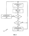
- FIG. 4 shows an exemplary filter control process 100 implemented by filter controller 22 according to one embodiment of the present invention.
- the receiver 10 determines the in-band signal power P s and the total output power P OUT (block 110) and provides the results to the filter controller 22.
- Filter controller 22 calculates an error value ⁇ based on the provided in-band and total powers P s , P OUT (block 120). More particularly, filter controller 22 calculates the current ratio ⁇ r according to Equation (4), and compares the current ratio ⁇ r to a limiting power ratio ⁇ o required for acceptable receiver performance to determine the error value ⁇ .
- Equation (4) the limiting power ratio ⁇ o represents a maximum power ratio
- the error value ⁇ may, for example, be given by Equation (5).
- a limiting power ratio ⁇ o for each defining communication standard may be pre-determined based on the standard-specific requirements for the in-band and blocking signal powers according to Equation (3) and stored in memory (not shown). These requirements may be static or dynamic, and thus, the limiting power ratio ⁇ o may also be static or dynamic.
- the error ⁇ represents how sufficient or insufficient the out-of-band attenuation of filter 14 is.
- the filter controller 22 When the error ⁇ is negative (block 130), the filter controller 22 generates a control signal U to increase the out-of-band attenuation of the filter 14 to decrease the power ratio of the blocking signals to the in-band signals at the expense of increased receiver power consumption (block 140).
- the filter controller 22 When the error ⁇ is positive (block 130) but greater than some predetermined threshold T (block 150), the filter controller 22 generates a control signal U to decrease the out-of-band attenuation of the filter 14 to reduce the power consumption of the filter (block 160) without compromising the existing power ratio of the blocking to the in-band signals.
- the filter controller 22 When the error ⁇ is positive (block 130) and less than the threshold T (block 150), the filter controller 22 generates a control signal U that maintains the current operating parameters of the filter 14.
- the threshold T of block 150 provides optional hysteresis control with respect to the error ⁇ .
- a negative error ⁇ indicates that the power ratio ⁇ r between the blocking and in-band signals is too large. Thus, for a negative error ⁇ , the amount of out-of-band attenuation may be increased unconditionally.
- a positive error ⁇ indicates that the power ratio ⁇ r between the blocking and in-band signals is smaller than necessary for acceptable receiver performance.
- the filter controller 22 may either maintain the current filter configuration or may decrease the out-of-band attenuation.
- the threshold T may be used to provide hysteresis to avoid oscillation around the optimal attenuation setting. It will be appreciated that when the threshold T is set to zero, the process 100 of Figure 4 eliminates block 150.
- Filter controller 22 may modify the out-of-band attenuation by modifying the filter transfer function A ( f b ) for out-of band signals, by modifying the order of the filter 14, by rearranging the poles and/or zeros in the filter 14, and/or by modifying the passband gain of the filter 14 relative to the out-of-band attenuation.
- filter 14 comprises a Butterworth filter and filter controller 22 directly translates the error signal ⁇ to a control signal U that in turn corresponds to the order of the Butterworth filter 14.
- the worst-case scenario for the filter 14 in this example may be defined by a 5 MHz in-band signal at a minimum level of -74 dBm ( P s ) and a 20 MHz blocking signal at -52 dBm ( P b ).
- the bandwidth of filter 14 ( f c ) is 10 MHz.
- the worst-case filter scenario may be derived from the performance requirements of the filter 14. Under these conditions, a controlling standard may require the blocking signal to be attenuated by 30 dB.
- FIG. 5 shows four different input signal scenarios, where all four scenarios have the same in-band signal power level ( P s ) but different blocking signal power levels ( P b ).
- the power levels for the different scenarios are numbered 1, 2, 3, or 4 depending on the scenario.
- the first scenario represents the worst-case scenario and lasts for 10 ⁇ s. Between 10 ⁇ s and 20 ⁇ s, the blocking signal has the same power level but has moved from 20 MHz to 40 MHz. Between 20 ⁇ s and 30 ⁇ s the blocking signal stays at 40 MHz but decreases in power from -52 dBm to -62 dBm. Between 30 ⁇ s and 40 ⁇ s, the blocking signal disappears entirely.
- the means by which the order of the filter 14 is changed may be as simple as decreasing and increasing the order by a fixed amount based on the sign of the error ⁇ (see the process 100 of Figure 4 ).
- the filter order may be limited by the range implemented in the filter 14, and therefore, the result obtained by Equation (7) may be limited to this range.
- the filter order changes irrespective of the magnitude of ⁇ n , and several iterations of the process 100 of Figure 4 may be required to reach the optimal solution.
- N n 5 - K N n - 1 + 1 ⁇ ⁇ n .
- N n is limited to the range [0, 1, 2, 3, 4, 5].
- Increasing/decreasing the attenuation of the blocking signal by changing the filter order is strongly dependent on the current and calculated order of the filter 14.
- any filter has an amplitude function that is inversely proportional to f b N . This is a very coarse approximation of any filter, but may none-the-less provide guidance on how to compensate for the attenuation dependency on the filter order. This dependency is partly addressed by Equation (9) by dividing the error signal ⁇ n by a previous filter order N n -1 +1.
- Equation (9) introduces a gain factor K as an additional means for controlling the step size in a fashion similar to ⁇ N of Equation (7).
- Higher gain factors K translate to larger step sizes towards the optimal solution (and therefore faster convergences), whereas lower gain factors translate to smaller step sizes (and therefore slower convergences). If the gain factor K is too large, the filter order may be overcompensated and may miss the optimal filter order. Therefore, the characteristics of the filter 14 used in practice will determine the optimal gain factor K. Given this, the gain factor K may generally be determined empirically through simulation.
- Figure 6 shows how the filter order changes for the above example when the gain factor K of Equation (9) is set to 60.
- Figure 7 shows the resulting filtered signals S OUT for the four different scenarios. As shown by Figure 7 , controlling the filter order based on the power ratio ⁇ r between the blocking and in-band signals provides the required receiver performance without requiring the receiver 10 to continuously operate under worst-case conditions.
- Figure 8 shows an alternate receiver 10 that measures the total output power P OUT in the analog domain and measures the in-band signal power P s in the digital domain.
- the channel selection filter 28 processes the digitized signal to obtain the desired in-band signal and the digital power detector 30 measures the power of the channel selection filter output to determine the in-band signal power P s .
- an analog power detector 32 measures the total power of the analog filter output signal S OUT to determine the total output power P OUT , e.g., using a sliding window detector to obtain an average total power of the analog filter output signal.
- analog power detector 32 may implement a translinear circuit technique or may comprise a basic multiplication circuit to obtain a linear representation of the total output power P OUT . If the filter controller 22 requires a logarithmic representation of the total output power P OUT , receiver 10 may further include a logarithmic amplifier (not shown) to convert the linear power value to a logarithmic power value.
- filter controller 22 takes into consideration the gain/attenuation of the amplifier 16, ADC 18, and channel selection filter 28 when determining the current power differential based on the total output power P OUT and the in-band signal power P s .
- the attenuation of the channel selection filter 28 is known, but the gain/attenuation of amplifier 16 and ADC 18 are estimated.
- the filter control accuracy depends on the accuracy of the gain/attenuation estimation of the amplifier 16 and ADC 18.
- the filter controller 22 of the present invention may run synchronously or asynchronously with the digital processor 20 depending on the receiver requirements. For example, if the controlling standard requires the filter controller 22 to adapt the filter parameters quickly, e.g., in a timeslot between received signal blocks, to accommodate fast variations in the input signal quality, the filter controller 22 may run synchronously with the processor 20. If the variations in the filter parameters are small enough such that the filter characteristics are generally constant over each received signal block in time and that the filter parameters may be treated as channel variations, the filter controller 22 may run asynchronously from the processor 20.
Landscapes
- Engineering & Computer Science (AREA)
- Computer Networks & Wireless Communication (AREA)
- Signal Processing (AREA)
- Circuits Of Receivers In General (AREA)
- Noise Elimination (AREA)
Claims (25)
- Verfahren zum Steuern des Stromverbrauchs eines Empfängers (10), das Folgendes umfasst:Filtern eines empfangenen Signals unter Verwendung eines variablen Filters (14) zum Generieren eines gefilterten Signals an einem Filterausgang; gekennzeichnet durchSteuern eines Stromverbrauchs des Empfängers (10) durch Steuern einer oder mehrerer Eigenschaften des variablen Filters (14) zum Aufrechterhalten eines momentanen Verhältnisses am Filterausgang zwischen einem oder mehreren ungewollten Außerband-Signalleistungspegeln und einem erwünschten Signalleistungspegel, dergestalt, dass das momentane Verhältnis ein zuvor festgelegtes Kriterium in Bezug auf einen erwünschten Verhältnispegel erfüllt.
- Verfahren nach Anspruch 1, wobei das Steuern des Stromverbrauchs des Empfängers (10) das Steuern einer oder mehrerer Eigenschaften des variablen Filters (14) zum Aufrechterhalten eines momentanen Verhältnisses am Filterausgang des einen oder der mehreren ungewollten Außerband-Signalleistungspegeln auf dem erwünschten Signalleistungspegel auf oder unter dem erwünschten Verhältnispegel umfasst.
- Verfahren nach Anspruch 1, das des Weiteren Folgendes umfasst:Messen einer Gesamtleistung und einer In-Band-Leistung des gefilterten Signals; undVergleichen der Gesamtleistung mit der In-Band-Leistung zum Bestimmen einer momentanen Leistungsdifferenz.
- Verfahren nach Anspruch 3, wobei das Steuern einer oder mehrerer Eigenschaften des variablen Filters (14) das Steuern einer oder mehrerer Eigenschaften des variablen Filters (14) umfasst, dergestalt, dass die momentane Leistungsdifferenz das zuvor festgelegte Kriterium in Bezug auf einen erwünschten Differenzpegel erfüllt.
- Verfahren nach Anspruch 3, wobei das Messen der Gesamtleistung und der In-Band-Leistung das digitale Messen der Gesamtleistung und der In-Band-Leistung des gefilterten Signals umfasst.
- Verfahren nach Anspruch 3, wobei das Messen der Gesamtleistung und der In-Band-Leistung das digitale Messen der In-Band-Leistung des gefilterten Signals und das Erhalten einer analogen Messung der Gesamtleistung des gefilterten Signals umfasst.
- Verfahren nach Anspruch 3, wobei das Vergleichen der Gesamtleistung mit der In-Band-Leistung das Ermitteln der momentanen Leistungsdifferenz anhand eines Verhältnisses zwischen der Gesamtleistung und der In-Band-Leistung umfasst.
- Verfahren nach Anspruch 3, wobei das Vergleichen der Gesamtleistung mit der In-Band-Leistung das Ermitteln der momentanen Leistungsdifferenz anhand einer Differenz zwischen der Gesamtleistung und der In-Band-Leistung umfasst.
- Verfahren nach Anspruch 3, das des Weiteren Folgendes umfasst:Ermitteln einer einschränkenden Leistungsdifferenz anhand von Anforderungen für einen steuernden Kommunikationsstandard; undVergleichen der einschränkenden Leistungsdifferenz mit der momentanen Leistungsdifferenz zum Bestimmen eines Fehlersignals,wobei das Steuern einer oder mehrerer Eigenschaften des variablen Filters das Steuern einer oder mehrerer Eigenschaften des variablen Filters anhand des Fehlersignals umfasst.
- Verfahren nach Anspruch 1, wobei das Steuern einer oder mehrerer Eigenschaften des variablen Filters (14) das Steuern einer Ordnung des variablen Filters (14) umfasst.
- Verfahren nach Anspruch 1, wobei das Steuern einer oder mehrerer Eigenschaften des variablen Filters (14) das Steuern einer Transferfunktion des variablen Filters (14) umfasst.
- Verfahren nach Anspruch 1, wobei das Steuern einer oder mehrerer Eigenschaften des variablen Filters (14) das Steuern einer Durchlassbandverstärkung des variablen Filters (14) in Bezug auf eine Außer-Band-Dämpfung des Filters (14) umfasst.
- Filtersystem, das dafür konfiguriert ist, den Stromverbrauch eines Empfängers (10) zu steuern, wobei das Filtersystem Folgendes umfasst:ein variables Filter (14), das dafür konfiguriert ist, ein empfangenes Signal zu filtern, um ein gefiltertes Signal an einem Filterausgang zu generieren; gekennzeichnet durcheine Steuereinheit (22), die dafür konfiguriert ist, einen Stromverbrauch des Empfängers (10) zu steuern, indem eine oder mehrere Eigenschaften des variablen Filters (14) gesteuert werden, um ein momentanes Verhältnis zwischen einem oder mehreren ungewollten Außerband-Signalleistungspegeln am Filterausgang und einem erwünschten Signalleistungspegel am Filterausgang aufrecht zu erhalten, dergestalt, dass das momentane Verhältnis ein zuvor festgelegtes Kriterium in Bezug auf einen erwünschten Verhältnispegel erfüllt.
- Filtersystem nach Anspruch 13, wobei die Steuereinheit (22) den Stromverbrauch des Empfängers (10) steuert, indem eine oder mehrere Eigenschaften des variablen Filters (14) gesteuert werden, um ein momentanes Verhältnis des einen oder der mehreren ungewollten Außerband-Signalleistungspegel am Filterausgang auf dem erwünschten Signalleistungspegel am Filterausgang auf oder unter einem erwünschten Verhältnispegel aufrecht zu erhalten.
- Filtersystem nach Anspruch 13, das des Weiteren ein oder mehrere Leistungsmessungselemente (30, 32) umfasst, die dafür konfiguriert sind, eine Gesamtleistung und eine In-Band-Leistung des gefilterten Signals zu messen, wobei die Steuereinheit (22) des Weiteren dafür konfiguriert ist, eine momentane Leistungsdifferenz anhand eines Vergleichs zwischen der Gesamtleistung und der In-Band-Leistung festzustellen.
- Filtersystem nach Anspruch 15, wobei die Steuereinheit (22) eine oder mehrere Eigenschaften des variablen Filters (14) steuert, indem eine oder mehrere Eigenschaften des variablen Filters (14) dergestalt gesteuert werden, dass die momentane Leistungsdifferenz das zuvor festgelegte Kriterium in Bezug auf einen erwünschten Differenzpegel erfüllt.
- Filtersystem nach Anspruch 15, wobei die Leistungsmessungselemente (30) einen oder mehrere digitale Leistungsdetektoren (30) umfassen, die dafür konfiguriert ist, die Gesamtleistung und die In-Band-Leistung des gefilterten Signals digital zu messen.
- Filtersystem nach Anspruch 15, wobei die Leistungsmessungselemente (30, 32) Folgendes umfassen:einen digital Leistungsdetektor (30), der dafür konfiguriert ist, die In-Band-Leistung des gefilterten Signals digital zu messen; undeinen analogen Leistungsdetektor (32), der dafür konfiguriert ist, eine analoge Messung der Gesamtleistung des gefilterten Signals zu erhalten.
- Filtersystem nach Anspruch 15, wobei die Steuereinheit (22) dafür konfiguriert ist, die momentane Leistungsdifferenz anhand eines Verhältnisses zwischen der Gesamtleistung und der In-Band-Leistung festzustellen.
- Filtersystem nach Anspruch 15, wobei die Steuereinheit (22) dafür konfiguriert ist, die momentane Leistungsdifferenz anhand einer Differenz zwischen der Gesamtleistung und der In-Band-Leistung festzustellen.
- Filtersystem nach Anspruch 15, wobei die Steuereinheit (22) des Weiteren dafür konfiguriert ist:eine einschränkende Leistungsdifferenz anhand von Anforderungen für einen steuernden Kommunikationsstandard zu bestimmen; unddie einschränkende Leistungsdifferenz mit der momentanen Leistungsdifferenz zu vergleichen, um ein Fehlersignal zu bestimmen,wobei die Steuereinheit (22) die Eigenschaften des variablen Filters (14) durch Steuern einer oder mehrerer Eigenschaften des variablen Filters (14) anhand des Fehlersignals steuert.
- Filtersystem nach Anspruch 13, wobei die Steuereinheit (22) dafür konfiguriert ist, eine Ordnung des variablen Filters (14) zu steuern.
- Filtersystem nach Anspruch 13, wobei die Steuereinheit (22) dafür konfiguriert ist, eine Transferfunktion des variablen Filters (14) zu steuern.
- Filtersystem nach Anspruch 13, wobei die Steuereinheit (22) dafür konfiguriert ist, eine Durchlassbandverstärkung des variablen Filters (14) in Bezug auf eine Außer-Band-Dämpfung des Filters (14) zu steuern.
- Drahtlosempfänger (10), der das Filtersystem nach einem der Ansprüche 13 umfasst.
Applications Claiming Priority (2)
| Application Number | Priority Date | Filing Date | Title |
|---|---|---|---|
| US12/057,924 US7979049B2 (en) | 2008-03-28 | 2008-03-28 | Automatic filter control |
| PCT/EP2009/053210 WO2009118263A1 (en) | 2008-03-28 | 2009-03-18 | Automatic filter control |
Publications (2)
| Publication Number | Publication Date |
|---|---|
| EP2255447A1 EP2255447A1 (de) | 2010-12-01 |
| EP2255447B1 true EP2255447B1 (de) | 2014-08-13 |
Family
ID=40736026
Family Applications (1)
| Application Number | Title | Priority Date | Filing Date |
|---|---|---|---|
| EP09723830.7A Active EP2255447B1 (de) | 2008-03-28 | 2009-03-18 | Automatische filtersteuerung |
Country Status (7)
| Country | Link |
|---|---|
| US (1) | US7979049B2 (de) |
| EP (1) | EP2255447B1 (de) |
| JP (1) | JP5554769B2 (de) |
| CN (1) | CN101981814B (de) |
| BR (1) | BRPI0909454A2 (de) |
| WO (1) | WO2009118263A1 (de) |
| ZA (1) | ZA201006268B (de) |
Families Citing this family (17)
| Publication number | Priority date | Publication date | Assignee | Title |
|---|---|---|---|---|
| EP2210352B1 (de) * | 2007-10-24 | 2020-05-06 | LifeSignals, Inc. | Systeme und netze für drahtlose halb- und vollduplexkommunikation unter verwendung mehrerer funkgeräte |
| WO2009100401A2 (en) * | 2008-02-06 | 2009-08-13 | Hmicro, Inc. | Wireless communications systems using multiple radios |
| US8417204B2 (en) * | 2008-05-07 | 2013-04-09 | Broadcom Corporation | Method and system for on-demand signal notching in a receiver |
| US8929492B2 (en) | 2009-12-03 | 2015-01-06 | Glowlink Communications Technology, Inc. | System for and method of removing unwanted inband signals from a received communication signal |
| US9537521B2 (en) | 2009-12-03 | 2017-01-03 | Glowlink Communications Technology, Inc. | System for and method of removing unwanted inband signals from a received communication signal |
| US8842791B2 (en) * | 2011-08-13 | 2014-09-23 | Posedge Inc. | Synchronization of a receiver to a desired signal |
| US9275690B2 (en) | 2012-05-30 | 2016-03-01 | Tahoe Rf Semiconductor, Inc. | Power management in an electronic system through reducing energy usage of a battery and/or controlling an output power of an amplifier thereof |
| US9509351B2 (en) | 2012-07-27 | 2016-11-29 | Tahoe Rf Semiconductor, Inc. | Simultaneous accommodation of a low power signal and an interfering signal in a radio frequency (RF) receiver |
| SG11201506441VA (en) * | 2013-02-26 | 2015-09-29 | Glowlink Communications Technology Inc | System for and method of removing unwanted inband signals from a received communication signal |
| US9837714B2 (en) | 2013-03-15 | 2017-12-05 | Integrated Device Technology, Inc. | Extending beamforming capability of a coupled voltage controlled oscillator (VCO) array during local oscillator (LO) signal generation through a circular configuration thereof |
| US9716315B2 (en) | 2013-03-15 | 2017-07-25 | Gigpeak, Inc. | Automatic high-resolution adaptive beam-steering |
| US9184498B2 (en) | 2013-03-15 | 2015-11-10 | Gigoptix, Inc. | Extending beamforming capability of a coupled voltage controlled oscillator (VCO) array during local oscillator (LO) signal generation through fine control of a tunable frequency of a tank circuit of a VCO thereof |
| US9531070B2 (en) | 2013-03-15 | 2016-12-27 | Christopher T. Schiller | Extending beamforming capability of a coupled voltage controlled oscillator (VCO) array during local oscillator (LO) signal generation through accommodating differential coupling between VCOs thereof |
| US9666942B2 (en) | 2013-03-15 | 2017-05-30 | Gigpeak, Inc. | Adaptive transmit array for beam-steering |
| US9722310B2 (en) | 2013-03-15 | 2017-08-01 | Gigpeak, Inc. | Extending beamforming capability of a coupled voltage controlled oscillator (VCO) array during local oscillator (LO) signal generation through frequency multiplication |
| US9780449B2 (en) | 2013-03-15 | 2017-10-03 | Integrated Device Technology, Inc. | Phase shift based improved reference input frequency signal injection into a coupled voltage controlled oscillator (VCO) array during local oscillator (LO) signal generation to reduce a phase-steering requirement during beamforming |
| CN117519388A (zh) * | 2023-11-30 | 2024-02-06 | 聚辰半导体股份有限公司 | 一种数字ldo结构 |
Family Cites Families (35)
| Publication number | Priority date | Publication date | Assignee | Title |
|---|---|---|---|---|
| JPH05304485A (ja) * | 1992-04-27 | 1993-11-16 | Nippon Telegr & Teleph Corp <Ntt> | 受信機 |
| US5646569A (en) | 1995-08-30 | 1997-07-08 | Hewlett-Packard Company | Method and apparatus for AC coupling |
| KR100193842B1 (ko) * | 1996-09-13 | 1999-06-15 | 윤종용 | 무선통신시스템의 전력조절 회로 및 방법 |
| US6026288A (en) * | 1996-12-10 | 2000-02-15 | Lucent Technologies, Inc. | Communications system with an apparatus for controlling overall power consumption based on received signal strength |
| JPH11274946A (ja) * | 1998-03-20 | 1999-10-08 | Mitsumi Electric Co Ltd | 送信回路 |
| JP3809302B2 (ja) * | 1999-06-29 | 2006-08-16 | 株式会社東芝 | フィルタ装置および無線受信装置 |
| US6816003B2 (en) * | 2000-02-04 | 2004-11-09 | The Trustees Of Columbia University In The City Of New York | Circuits with dynamic biasing |
| US6782062B1 (en) * | 2000-03-29 | 2004-08-24 | Sony Corporation | Low power and high linearity receivers with reactively biased front ends |
| US7274760B2 (en) * | 2000-08-01 | 2007-09-25 | George Palaskas | Circuit and method for dynamically modifiable signal processor |
| WO2002056470A1 (en) * | 2001-01-10 | 2002-07-18 | The Trustees Of Columbia University In The City Of New York | Active filter circuit with dynamically modifiable gain |
| US20020177446A1 (en) | 2001-05-23 | 2002-11-28 | Alex Bugeja | System and method for providing variable transmission bandwidth over communications channels |
| US7209528B2 (en) | 2001-06-01 | 2007-04-24 | National Semiconductor, Inc. | Over-sampling A/D converter with adjacent channel power detection |
| US6670901B2 (en) | 2001-07-31 | 2003-12-30 | Motorola, Inc. | Dynamic range on demand receiver and method of varying same |
| US6577258B2 (en) | 2001-10-01 | 2003-06-10 | Nokia Corporation | Adaptive sigma-delta data converter for mobile terminals |
| US6876635B2 (en) * | 2001-11-05 | 2005-04-05 | Motorola, Inc. | Current reduction by receiver linearity adjustment in a communication device |
| US6512472B1 (en) | 2002-01-15 | 2003-01-28 | Motorola, Inc. | Method and apparatus for optimizing dynamic range of a wideband analog-to-digital converter |
| US6687491B2 (en) * | 2002-01-18 | 2004-02-03 | Sony Corporation | Direct conversion of low power high linearity receiver |
| US7130364B2 (en) | 2002-01-31 | 2006-10-31 | Nokia Corporation | Interference dependent ADC headroom adjustment |
| JP2003298441A (ja) * | 2002-04-01 | 2003-10-17 | Hitachi Ltd | 低消費電力受信装置 |
| EP1363403B8 (de) | 2002-05-16 | 2005-10-19 | Sony Deutschland GmbH | Empfangsvorrichtung mit automatischer Verstärkungsregelung |
| US7212592B2 (en) | 2002-05-20 | 2007-05-01 | Ati Technologies Inc. | Digitally programmable gain control circuit |
| GB2394133A (en) | 2002-10-17 | 2004-04-14 | Toumaz Technology Ltd | Radio receiver with reconfigurable filtering arrangement |
| US7010330B1 (en) | 2003-03-01 | 2006-03-07 | Theta Microelectronics, Inc. | Power dissipation reduction in wireless transceivers |
| JP3711117B2 (ja) * | 2003-03-25 | 2005-10-26 | 株式会社東芝 | 無線受信装置 |
| CN1549454A (zh) | 2003-05-16 | 2004-11-24 | 皇家飞利浦电子股份有限公司 | 具有一个有限动态范围的adc的无线通信接收机 |
| US8401128B2 (en) | 2003-08-28 | 2013-03-19 | Telefonaktiebolaget L M Ericsson (Publ) | Method and system for adaptable receiver parameters |
| US6894632B1 (en) | 2004-01-14 | 2005-05-17 | Northrop Grumman Corporation | Programmable analog-to-digital converter |
| JP2007526712A (ja) | 2004-03-02 | 2007-09-13 | コーニンクレッカ フィリップス エレクトロニクス エヌ ヴィ | 入力信号に依存する信号状態 |
| JP2005295348A (ja) * | 2004-04-02 | 2005-10-20 | Sharp Corp | 受信機 |
| US7439890B2 (en) | 2005-08-09 | 2008-10-21 | Analog Devices, Inc. | ΔΣ analog to digital converter system with automatic gain control responsive to out-of-band interferers |
| US8951190B2 (en) | 2005-09-28 | 2015-02-10 | Zin Technologies, Inc. | Transfer function control for biometric monitoring system |
| JP2007184693A (ja) * | 2006-01-05 | 2007-07-19 | Toshiba Corp | Fmチューナ |
| JP4687510B2 (ja) * | 2006-03-08 | 2011-05-25 | 日本電気株式会社 | 移動通信端末における信号処理システム及びその方法並びにそれを用いた移動通信端末 |
| US8781426B2 (en) | 2006-05-15 | 2014-07-15 | Qualcomm Incorporated | Techniques for controlling operation of control loops in a receiver |
| JP2008042765A (ja) * | 2006-08-09 | 2008-02-21 | Sharp Corp | 受信システム |
-
2008
- 2008-03-28 US US12/057,924 patent/US7979049B2/en active Active
-
2009
- 2009-03-18 BR BRPI0909454A patent/BRPI0909454A2/pt not_active Application Discontinuation
- 2009-03-18 EP EP09723830.7A patent/EP2255447B1/de active Active
- 2009-03-18 WO PCT/EP2009/053210 patent/WO2009118263A1/en not_active Ceased
- 2009-03-18 CN CN200980112367.XA patent/CN101981814B/zh active Active
- 2009-03-18 JP JP2011501179A patent/JP5554769B2/ja active Active
-
2010
- 2010-09-01 ZA ZA2010/06268A patent/ZA201006268B/en unknown
Also Published As
| Publication number | Publication date |
|---|---|
| CN101981814A (zh) | 2011-02-23 |
| WO2009118263A1 (en) | 2009-10-01 |
| US7979049B2 (en) | 2011-07-12 |
| US20090245438A1 (en) | 2009-10-01 |
| EP2255447A1 (de) | 2010-12-01 |
| ZA201006268B (en) | 2011-11-30 |
| CN101981814B (zh) | 2014-07-02 |
| JP5554769B2 (ja) | 2014-07-23 |
| JP2011515975A (ja) | 2011-05-19 |
| BRPI0909454A2 (pt) | 2015-12-22 |
Similar Documents
| Publication | Publication Date | Title |
|---|---|---|
| US7979049B2 (en) | Automatic filter control | |
| EP2810370B1 (de) | Verfahren und vorrichtung zur unabhängigen steuerung einer front-end-verstärkung und einer basisbandverstärkung | |
| US8675789B2 (en) | Receiver with variable gain elements and automatic gain control to maintain a positive signal to noise ratio margin | |
| EP2086269B1 (de) | Sendeleistungsregler | |
| CA2679600C (en) | Radio receiver having a multi-state variable threshold automatic gain control (agc) for fast channel scanning acquisition and method for using same | |
| US20030078007A1 (en) | Method and apparatus for continuously controlling the dynamic range from an analog-to-digital converter | |
| US20130324065A1 (en) | Method and Apparatus for Auto Gain Control in Radio Receiver | |
| US7929650B2 (en) | AGC for narrowband receivers | |
| EP1841061A2 (de) | Verstärkungsregelungsverfahren und Vorrichtung im Empfänger eines drahtlosen Kommunikationssystems | |
| EP3783804B1 (de) | Automatische verstärkungsregelung zur optimierung der empfängerleistung in gegenwart von störsignalen | |
| WO2010014822A2 (en) | Jammer detection with mitigation of detection threshold hysteresis pinch-off effect | |
| EP1434345B1 (de) | Nachrichtenübertragungsempfänger mit automatischer Verstärkungsregelung | |
| KR20090087989A (ko) | 자동이득제어 정보를 이용한 전력소모 감소장치가 구비된수신기 및 이를 이용한 전력소모 감소방법 | |
| EP2608404B1 (de) | Verfahren und Vorrichtung zur Durchführung einer automatischen Verstärkungsregelung eines empfangenen Signals | |
| US7983642B2 (en) | Method and system for detecting an out of band interferer in an RF receiver | |
| US8676140B2 (en) | Efficient scheme for automatic gain control in communication systems | |
| US7277510B1 (en) | Adaptation algorithm based on signal statistics for automatic gain control | |
| WO2015157604A1 (en) | Method and apparatus for adaptive automatic gain control | |
| US7054607B2 (en) | Method and apparatus for reducing DC offset in a wireless receiver | |
| US20170077886A1 (en) | Rf tuner with blocker detection and noise limited region recovery | |
| WO2007098235A2 (en) | Optimally adaptive receiver | |
| US20080013655A1 (en) | Apparatus and method for automatic gain control | |
| KR101040989B1 (ko) | Gps 시스템에 있어서 안티-재밍을 위한 배열안테나의 이득 및 대역폭 조절 장치 및 방법 | |
| US8300732B1 (en) | DC offset removal using digital feedback | |
| EP1499014A1 (de) | Verfahren zur automatischen Verstärkungsregelung, beispielsweise in einem Telekommunikationssystem, Vorrichtung und Computerprogramm hierfür |
Legal Events
| Date | Code | Title | Description |
|---|---|---|---|
| PUAI | Public reference made under article 153(3) epc to a published international application that has entered the european phase |
Free format text: ORIGINAL CODE: 0009012 |
|
| 17P | Request for examination filed |
Effective date: 20100915 |
|
| AK | Designated contracting states |
Kind code of ref document: A1 Designated state(s): AT BE BG CH CY CZ DE DK EE ES FI FR GB GR HR HU IE IS IT LI LT LU LV MC MK MT NL NO PL PT RO SE SI SK TR |
|
| AX | Request for extension of the european patent |
Extension state: AL BA RS |
|
| 17Q | First examination report despatched |
Effective date: 20110315 |
|
| DAX | Request for extension of the european patent (deleted) | ||
| REG | Reference to a national code |
Ref country code: DE Ref legal event code: R079 Ref document number: 602009025942 Country of ref document: DE Free format text: PREVIOUS MAIN CLASS: H04B0001160000 Ipc: H04W0052020000 |
|
| RIC1 | Information provided on ipc code assigned before grant |
Ipc: H04W 52/02 20090101AFI20140217BHEP |
|
| GRAP | Despatch of communication of intention to grant a patent |
Free format text: ORIGINAL CODE: EPIDOSNIGR1 |
|
| RAP1 | Party data changed (applicant data changed or rights of an application transferred) |
Owner name: TELEFONAKTIEBOLAGET L M ERICSSON (PUBL) |
|
| INTG | Intention to grant announced |
Effective date: 20140409 |
|
| GRAS | Grant fee paid |
Free format text: ORIGINAL CODE: EPIDOSNIGR3 |
|
| GRAA | (expected) grant |
Free format text: ORIGINAL CODE: 0009210 |
|
| AK | Designated contracting states |
Kind code of ref document: B1 Designated state(s): AT BE BG CH CY CZ DE DK EE ES FI FR GB GR HR HU IE IS IT LI LT LU LV MC MK MT NL NO PL PT RO SE SI SK TR |
|
| REG | Reference to a national code |
Ref country code: GB Ref legal event code: FG4D |
|
| REG | Reference to a national code |
Ref country code: CH Ref legal event code: EP Ref country code: AT Ref legal event code: REF Ref document number: 682863 Country of ref document: AT Kind code of ref document: T Effective date: 20140815 |
|
| REG | Reference to a national code |
Ref country code: IE Ref legal event code: FG4D |
|
| REG | Reference to a national code |
Ref country code: DE Ref legal event code: R096 Ref document number: 602009025942 Country of ref document: DE Effective date: 20140918 |
|
| REG | Reference to a national code |
Ref country code: NL Ref legal event code: T3 |
|
| REG | Reference to a national code |
Ref country code: LT Ref legal event code: MG4D |
|
| PG25 | Lapsed in a contracting state [announced via postgrant information from national office to epo] |
Ref country code: ES Free format text: LAPSE BECAUSE OF FAILURE TO SUBMIT A TRANSLATION OF THE DESCRIPTION OR TO PAY THE FEE WITHIN THE PRESCRIBED TIME-LIMIT Effective date: 20140813 Ref country code: BG Free format text: LAPSE BECAUSE OF FAILURE TO SUBMIT A TRANSLATION OF THE DESCRIPTION OR TO PAY THE FEE WITHIN THE PRESCRIBED TIME-LIMIT Effective date: 20141113 Ref country code: LT Free format text: LAPSE BECAUSE OF FAILURE TO SUBMIT A TRANSLATION OF THE DESCRIPTION OR TO PAY THE FEE WITHIN THE PRESCRIBED TIME-LIMIT Effective date: 20140813 Ref country code: PT Free format text: LAPSE BECAUSE OF FAILURE TO SUBMIT A TRANSLATION OF THE DESCRIPTION OR TO PAY THE FEE WITHIN THE PRESCRIBED TIME-LIMIT Effective date: 20141215 Ref country code: SE Free format text: LAPSE BECAUSE OF FAILURE TO SUBMIT A TRANSLATION OF THE DESCRIPTION OR TO PAY THE FEE WITHIN THE PRESCRIBED TIME-LIMIT Effective date: 20140813 Ref country code: NO Free format text: LAPSE BECAUSE OF FAILURE TO SUBMIT A TRANSLATION OF THE DESCRIPTION OR TO PAY THE FEE WITHIN THE PRESCRIBED TIME-LIMIT Effective date: 20141113 Ref country code: GR Free format text: LAPSE BECAUSE OF FAILURE TO SUBMIT A TRANSLATION OF THE DESCRIPTION OR TO PAY THE FEE WITHIN THE PRESCRIBED TIME-LIMIT Effective date: 20141114 Ref country code: FI Free format text: LAPSE BECAUSE OF FAILURE TO SUBMIT A TRANSLATION OF THE DESCRIPTION OR TO PAY THE FEE WITHIN THE PRESCRIBED TIME-LIMIT Effective date: 20140813 |
|
| PG25 | Lapsed in a contracting state [announced via postgrant information from national office to epo] |
Ref country code: CY Free format text: LAPSE BECAUSE OF FAILURE TO SUBMIT A TRANSLATION OF THE DESCRIPTION OR TO PAY THE FEE WITHIN THE PRESCRIBED TIME-LIMIT Effective date: 20140813 Ref country code: LV Free format text: LAPSE BECAUSE OF FAILURE TO SUBMIT A TRANSLATION OF THE DESCRIPTION OR TO PAY THE FEE WITHIN THE PRESCRIBED TIME-LIMIT Effective date: 20140813 Ref country code: HR Free format text: LAPSE BECAUSE OF FAILURE TO SUBMIT A TRANSLATION OF THE DESCRIPTION OR TO PAY THE FEE WITHIN THE PRESCRIBED TIME-LIMIT Effective date: 20140813 Ref country code: IS Free format text: LAPSE BECAUSE OF FAILURE TO SUBMIT A TRANSLATION OF THE DESCRIPTION OR TO PAY THE FEE WITHIN THE PRESCRIBED TIME-LIMIT Effective date: 20141213 |
|
| PG25 | Lapsed in a contracting state [announced via postgrant information from national office to epo] |
Ref country code: RO Free format text: LAPSE BECAUSE OF FAILURE TO SUBMIT A TRANSLATION OF THE DESCRIPTION OR TO PAY THE FEE WITHIN THE PRESCRIBED TIME-LIMIT Effective date: 20140813 Ref country code: DK Free format text: LAPSE BECAUSE OF FAILURE TO SUBMIT A TRANSLATION OF THE DESCRIPTION OR TO PAY THE FEE WITHIN THE PRESCRIBED TIME-LIMIT Effective date: 20140813 Ref country code: SK Free format text: LAPSE BECAUSE OF FAILURE TO SUBMIT A TRANSLATION OF THE DESCRIPTION OR TO PAY THE FEE WITHIN THE PRESCRIBED TIME-LIMIT Effective date: 20140813 Ref country code: CZ Free format text: LAPSE BECAUSE OF FAILURE TO SUBMIT A TRANSLATION OF THE DESCRIPTION OR TO PAY THE FEE WITHIN THE PRESCRIBED TIME-LIMIT Effective date: 20140813 Ref country code: EE Free format text: LAPSE BECAUSE OF FAILURE TO SUBMIT A TRANSLATION OF THE DESCRIPTION OR TO PAY THE FEE WITHIN THE PRESCRIBED TIME-LIMIT Effective date: 20140813 |
|
| REG | Reference to a national code |
Ref country code: DE Ref legal event code: R097 Ref document number: 602009025942 Country of ref document: DE |
|
| PG25 | Lapsed in a contracting state [announced via postgrant information from national office to epo] |
Ref country code: PL Free format text: LAPSE BECAUSE OF FAILURE TO SUBMIT A TRANSLATION OF THE DESCRIPTION OR TO PAY THE FEE WITHIN THE PRESCRIBED TIME-LIMIT Effective date: 20140813 |
|
| PLBE | No opposition filed within time limit |
Free format text: ORIGINAL CODE: 0009261 |
|
| STAA | Information on the status of an ep patent application or granted ep patent |
Free format text: STATUS: NO OPPOSITION FILED WITHIN TIME LIMIT |
|
| 26N | No opposition filed |
Effective date: 20150515 |
|
| PG25 | Lapsed in a contracting state [announced via postgrant information from national office to epo] |
Ref country code: LU Free format text: LAPSE BECAUSE OF FAILURE TO SUBMIT A TRANSLATION OF THE DESCRIPTION OR TO PAY THE FEE WITHIN THE PRESCRIBED TIME-LIMIT Effective date: 20150318 Ref country code: MC Free format text: LAPSE BECAUSE OF FAILURE TO SUBMIT A TRANSLATION OF THE DESCRIPTION OR TO PAY THE FEE WITHIN THE PRESCRIBED TIME-LIMIT Effective date: 20140813 |
|
| REG | Reference to a national code |
Ref country code: CH Ref legal event code: PL |
|
| PG25 | Lapsed in a contracting state [announced via postgrant information from national office to epo] |
Ref country code: SI Free format text: LAPSE BECAUSE OF FAILURE TO SUBMIT A TRANSLATION OF THE DESCRIPTION OR TO PAY THE FEE WITHIN THE PRESCRIBED TIME-LIMIT Effective date: 20140813 |
|
| REG | Reference to a national code |
Ref country code: FR Ref legal event code: ST Effective date: 20151130 |
|
| REG | Reference to a national code |
Ref country code: IE Ref legal event code: MM4A |
|
| PG25 | Lapsed in a contracting state [announced via postgrant information from national office to epo] |
Ref country code: LI Free format text: LAPSE BECAUSE OF NON-PAYMENT OF DUE FEES Effective date: 20150331 Ref country code: CH Free format text: LAPSE BECAUSE OF NON-PAYMENT OF DUE FEES Effective date: 20150331 Ref country code: IE Free format text: LAPSE BECAUSE OF NON-PAYMENT OF DUE FEES Effective date: 20150318 |
|
| PG25 | Lapsed in a contracting state [announced via postgrant information from national office to epo] |
Ref country code: FR Free format text: LAPSE BECAUSE OF NON-PAYMENT OF DUE FEES Effective date: 20150331 |
|
| PG25 | Lapsed in a contracting state [announced via postgrant information from national office to epo] |
Ref country code: MT Free format text: LAPSE BECAUSE OF FAILURE TO SUBMIT A TRANSLATION OF THE DESCRIPTION OR TO PAY THE FEE WITHIN THE PRESCRIBED TIME-LIMIT Effective date: 20140813 |
|
| PG25 | Lapsed in a contracting state [announced via postgrant information from national office to epo] |
Ref country code: HU Free format text: LAPSE BECAUSE OF FAILURE TO SUBMIT A TRANSLATION OF THE DESCRIPTION OR TO PAY THE FEE WITHIN THE PRESCRIBED TIME-LIMIT; INVALID AB INITIO Effective date: 20090318 |
|
| PG25 | Lapsed in a contracting state [announced via postgrant information from national office to epo] |
Ref country code: TR Free format text: LAPSE BECAUSE OF FAILURE TO SUBMIT A TRANSLATION OF THE DESCRIPTION OR TO PAY THE FEE WITHIN THE PRESCRIBED TIME-LIMIT Effective date: 20140813 |
|
| PG25 | Lapsed in a contracting state [announced via postgrant information from national office to epo] |
Ref country code: MK Free format text: LAPSE BECAUSE OF FAILURE TO SUBMIT A TRANSLATION OF THE DESCRIPTION OR TO PAY THE FEE WITHIN THE PRESCRIBED TIME-LIMIT Effective date: 20140813 |
|
| PGFP | Annual fee paid to national office [announced via postgrant information from national office to epo] |
Ref country code: AT Payment date: 20230303 Year of fee payment: 15 |
|
| PGFP | Annual fee paid to national office [announced via postgrant information from national office to epo] |
Ref country code: IT Payment date: 20230321 Year of fee payment: 15 |
|
| P01 | Opt-out of the competence of the unified patent court (upc) registered |
Effective date: 20230524 |
|
| REG | Reference to a national code |
Ref country code: AT Ref legal event code: MM01 Ref document number: 682863 Country of ref document: AT Kind code of ref document: T Effective date: 20240318 |
|
| PG25 | Lapsed in a contracting state [announced via postgrant information from national office to epo] |
Ref country code: AT Free format text: LAPSE BECAUSE OF NON-PAYMENT OF DUE FEES Effective date: 20240318 |
|
| PG25 | Lapsed in a contracting state [announced via postgrant information from national office to epo] |
Ref country code: AT Free format text: LAPSE BECAUSE OF NON-PAYMENT OF DUE FEES Effective date: 20240318 |
|
| PG25 | Lapsed in a contracting state [announced via postgrant information from national office to epo] |
Ref country code: IT Free format text: LAPSE BECAUSE OF NON-PAYMENT OF DUE FEES Effective date: 20240318 |
|
| PGFP | Annual fee paid to national office [announced via postgrant information from national office to epo] |
Ref country code: GB Payment date: 20260327 Year of fee payment: 18 |
|
| PGFP | Annual fee paid to national office [announced via postgrant information from national office to epo] |
Ref country code: DE Payment date: 20260327 Year of fee payment: 18 |
|
| PGFP | Annual fee paid to national office [announced via postgrant information from national office to epo] |
Ref country code: BE Payment date: 20260327 Year of fee payment: 18 |
|
| PGFP | Annual fee paid to national office [announced via postgrant information from national office to epo] |
Ref country code: NL Payment date: 20260326 Year of fee payment: 18 |