EP2248249B1 - Circuit d'attaque électronique et procédé - Google Patents
Circuit d'attaque électronique et procédé Download PDFInfo
- Publication number
- EP2248249B1 EP2248249B1 EP09706501.5A EP09706501A EP2248249B1 EP 2248249 B1 EP2248249 B1 EP 2248249B1 EP 09706501 A EP09706501 A EP 09706501A EP 2248249 B1 EP2248249 B1 EP 2248249B1
- Authority
- EP
- European Patent Office
- Prior art keywords
- buck
- voltage
- mains
- boost
- control
- Prior art date
- Legal status (The legal status is an assumption and is not a legal conclusion. Google has not performed a legal analysis and makes no representation as to the accuracy of the status listed.)
- Not-in-force
Links
Images


Classifications
-
- H—ELECTRICITY
- H05—ELECTRIC TECHNIQUES NOT OTHERWISE PROVIDED FOR
- H05B—ELECTRIC HEATING; ELECTRIC LIGHT SOURCES NOT OTHERWISE PROVIDED FOR; CIRCUIT ARRANGEMENTS FOR ELECTRIC LIGHT SOURCES, IN GENERAL
- H05B45/00—Circuit arrangements for operating light-emitting diodes [LED]
-
- H—ELECTRICITY
- H02—GENERATION; CONVERSION OR DISTRIBUTION OF ELECTRIC POWER
- H02M—APPARATUS FOR CONVERSION BETWEEN AC AND AC, BETWEEN AC AND DC, OR BETWEEN DC AND DC, AND FOR USE WITH MAINS OR SIMILAR POWER SUPPLY SYSTEMS; CONVERSION OF DC OR AC INPUT POWER INTO SURGE OUTPUT POWER; CONTROL OR REGULATION THEREOF
- H02M3/00—Conversion of dc power input into dc power output
- H02M3/02—Conversion of dc power input into dc power output without intermediate conversion into ac
- H02M3/04—Conversion of dc power input into dc power output without intermediate conversion into ac by static converters
- H02M3/10—Conversion of dc power input into dc power output without intermediate conversion into ac by static converters using discharge tubes with control electrode or semiconductor devices with control electrode
- H02M3/145—Conversion of dc power input into dc power output without intermediate conversion into ac by static converters using discharge tubes with control electrode or semiconductor devices with control electrode using devices of a triode or transistor type requiring continuous application of a control signal
- H02M3/155—Conversion of dc power input into dc power output without intermediate conversion into ac by static converters using discharge tubes with control electrode or semiconductor devices with control electrode using devices of a triode or transistor type requiring continuous application of a control signal using semiconductor devices only
- H02M3/156—Conversion of dc power input into dc power output without intermediate conversion into ac by static converters using discharge tubes with control electrode or semiconductor devices with control electrode using devices of a triode or transistor type requiring continuous application of a control signal using semiconductor devices only with automatic control of output voltage or current, e.g. switching regulators
- H02M3/158—Conversion of dc power input into dc power output without intermediate conversion into ac by static converters using discharge tubes with control electrode or semiconductor devices with control electrode using devices of a triode or transistor type requiring continuous application of a control signal using semiconductor devices only with automatic control of output voltage or current, e.g. switching regulators including plural semiconductor devices as final control devices for a single load
- H02M3/1582—Buck-boost converters
Definitions
- the present invention relates to an electronic driver circuit and a corresponding method of supplying an electronic load, in particular a number of LEDs or OLEDs coupled in series, with a DC current or voltage.
- LED lamps and luminaries are more and more penetrating the classical market segment of fluorescent and TL-Lamp applications.
- LED driver circuits include two or three individual power converters to operate LEDs with a DC current from AC mains grid. Thus, they have a high component count and moderate efficiency of about 80%.
- Applications with a power level above 25W usually include a second DC/DC boost converter to fulfill AC mains current harmonic standards, thus further increasing component count.
- a low component count and high efficiency is also of interest for the inverse transfer of power, for instance the transfer of a DC current from solar cells into an AC grid.
- a dual buck-boost DC/AC inverter is known from N. Vazquez et al., "Analysis and experimental study of the buck, boost and buck-boost inverters", Proceedings of the IEEE Power Electronics Specialist Conference, 1999, pp. 801-806 .
- this circuit has disadvantages due to its control principle.
- the two modulated DC voltages have a high peak value and there is a high internal power flow leading to a low efficiency.
- US 2007/0058402 A1 discloses a synchronous full bridge rectifier which is controlled to provide a power factor near unity.
- the full bridge rectifiers are transistors, each with a controlling input.
- the AC input signal and currents within the circuit are sensed and sent to a controller.
- the controller outputs control signals to turn on/off the rectifying MOSFETs timely to form a power factor of near one with respect to the AC input signal.
- the full wave rectifier is made of N-channel MOSFETs, some with fast body diodes.
- the MOSFETs are rectifiers and power factor circuit (PFC) control elements. The result is a one-stage synchronous rectifier with PFC.
- a solid state precision analogue differential amplifier senses the AC line waveform and high frequency current transformers sense the currents.
- the controller accepts the inputs of the amplifier and the sensed currents and outputs control signals that turn on and off the four MOSFETs.
- the timing of turning on/off is arranged so that the current drawn from the AC source is sinusoidal and matches the phase of the sinusoidal AC source.
- This special boost converter circuit generates a DC output voltage that is higher than the input voltage. For supplying a number of LEDs or OLEDs coupled in series, this circuit is not suited, however, since LEDs and OLEDs have a limited DC supply bus voltage. High DC bus voltages generate high electric fields in some series-connected LEDs or OLEDs that can damage these devices.
- an electronic driver circuit comprising:
- an electronic driving method comprising the steps of:
- the present invention is based on the idea to operate two buck-boost converters according to a dedicated dual-mode principle. This allows the integration of two functions, namely AC/DC rectification and DC/DC conversion in a single power converter. These two functions are alternately operated by the two buck-boost converters.
- the circuit and method according to the present invention offer a very high efficiency since power loss sources, like in e.g. a mains rectifier diode bridge, are not present.
- power loss sources like in e.g. a mains rectifier diode bridge
- a higher efficiency than with known dual buck-boost converters is obtained because of greatly reduced or no internal power flow.
- a higher efficiency than with known LED lamp drivers is obtained because of the absence of mains rectifier diodes.
- only a low thermal stress is exerted on the electronic load, e.g. LED or OLED lighting systems, from an integrated electronic driver.
- control unit is adapted for monitoring the sign of said AC input voltage. This provides a simple way of monitoring the zero crossings of the AC input voltage.
- the two buck-boost converters are adapted for alternately operating as synchronous rectifier, which leads to a further increase in efficiency. Still further, it is proposed that the two buck-boost converters are adapted for alternately operating as buck-boost converter.
- At least one of said two buck-boost converters comprises a power semiconductor, in particular a MOSFET transistor, a rectifier diode and a converter inductor.
- a power semiconductor in particular a MOSFET transistor, a rectifier diode and a converter inductor.
- At least one of said two buck-boost converters comprises a first power semiconductor, in particular a first MOSFET transistor, a second power semiconductor, in particular a second MOSFET transistor, and a converter inductor.
- a second power semiconductor is used as a synchronous rectifier instead of a rectifier diode, therebyt reducing power losses and increasing efficiency.
- At least one of said two buck-boost converters comprises a filtering capacitor for filtering the input current of said buck-boost converter.
- the control unit comprises, in one embodiment, a single control sub-unit for monitoring the zero crossing of the AC input voltage and controlling the respective buck-boost converter to change its mode of operation upon detection of a zero crossing.
- the control unit comprises two control sub-units, each being included in one of said two buck-boost converters for independently monitoring the zero crossing of the AC input voltage and controlling the respective buck-boost converter to change its mode of operation upon detection of a zero crossing.
- said control unit has an internal DC reference voltage and two comparators for turning on one power semiconductor as the power semiconductor of a buck-boost converter with a regulated output and the second power semiconductor as a synchronous rectifier.
- said control unit has an internal DC reference voltage and two comparators for turning on one power semiconductor as the power semiconductor of a buck-boost converter with a regulated output and the second power semiconductor as a synchronous rectifier.
- the electronic driver circuit further comprises a control loop for controlling the DC voltage supplied to said load, said control loop comprising:
- the load is supplied with a stabilized DC voltage controlled by control units that are allowed to have different electrical reference potentials for the DC input voltage (control unit terminal a) and the regulated DC output voltage (control unit terminal b).
- said control unit comprises a first control loop for controlling the DC voltage supplied to said electronic load and a second control loop for controlling the peak current in the buck-boost inductor, said control loops comprising:
- the load is supplied with a stabilized DC average current in combination with an AC mains current that has a high power factor, and both are controlled by control units that are allowed to have different electrical reference potentials for the DC input voltage (control unit terminal a) and the regulated DC output voltage (control unit terminal b).
- said control unit comprises a control loop for controlling the DC current supplied to said electronic load, plus a second control loop that controls the peak current in the buck-boost inductors, said control loop comprising:
- said first and second monitoring units comprise shunt resistors.
- said electronic driver circuit is adapted for supplying a number of LEDs and/or OLEDs with a DC current or DC voltage. Further, the electronic driver circuit generates an AC mains current with a high power factor close to one.
- Fig. 1 depicts a driver circuit that consists of an AC/DC mains rectifier as first conversion stage and a DC/DC flyback converter as second power conversion stage.
- This driver circuit supplies a series of LEDs, i.e. LED1, LED2, LED3, with a DC current from AC mains grid. It has, however, a high component count and a moderate efficiency of about 80%.
- Fig. 2 depicts a circuit diagram of a dual buck-boost DC/AC inverter known from N. Vazquez et al., "Analysis and experimental study of the buck, boost and buck-boost inverters", Proceedings of the IEEE Power Electronics Specialist Conference, 1999, pp. 801-806 .
- This circuit has disadvantages. Firstly, it generates two modulated DC voltages V a (t) and V b (t) that have a high peak value in excess of two times the peak output AC voltage as illustrated in Fig. 3 . Secondly, the multiplication of load current times modulated DC voltages V a (t) and V b (t) leads to an internal power flow as illustrated in Fig. 4 . This internal power flow increases conduction loss and thus the combination of this converter circuit with the proposed control technique does not result in high efficiency.
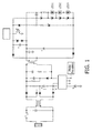
- FIG. 5 A circuit diagram of a first embodiment of an electronic driver circuit according to the present invention is depicted in Fig. 5 .
- the electronic driver circuit operates as a combined AC/DC and DC/DC converter and converts AC mains voltage V mains to a regulated DC voltage V load to supply an electronic load, here a number of LEDs: LED 1, LED2, ..., LEDn coupled in series, said driver circuit having a low component count and thus low cost as well as a high efficiency.
- the electronic driver circuit comprises two buck-boost converters 10, 20, each comprising control sub-units 11, 21, a power semiconductor Q1, Q2 (here a MOSFET transistor Q1, Q2), a rectifier diode D1, D2 coupled with one terminal to the drain terminal of the respective MOSFET transistor Q1, Q2 and with the other terminal to the +DC output terminal, and an inductor L1, L2 coupled between the drain terminal of the respective MOSFET transistor Q1, Q2 and the DC ground output terminal.
- a power semiconductor Q1, Q2 here a MOSFET transistor Q1, Q2
- a rectifier diode D1, D2 coupled with one terminal to the drain terminal of the respective MOSFET transistor Q1, Q2 and with the other terminal to the +DC output terminal
- an inductor L1, L2 coupled between the drain terminal of the respective MOSFET transistor Q1, Q2 and the DC ground output terminal.
- the control sub-units 11, 21 (depicted in more detail in Fig. 14 ) have five control terminals a, b, c, d and e.
- the control terminal a of control sub-unit 11 is coupled to the source terminal of MOSFET transistor Q1 and AC mains line terminal L.
- the control terminal a of control sub- unit 21 is coupled to the source terminal of MOSFET transistor Q2 and AC mains neutral terminal N.
- the control terminal b of both control sub-units is coupled to the DC ground output terminal.
- the control terminal c of control sub-unit 11 is coupled to AC mains neutral terminal N.
- the control terminal c of control sub-unit 21 is coupled to AC mains line terminal L.
- Control terminals d of both control sub-units are coupled to the +DC output terminal.
- An output filtering capacitor C3 is coupled between the DC output terminals.
- Input capacitors C1, C2 are coupled between the DC ground output terminal and the source terminal of the respective MOSFET transistor Q1, Q2 for filtering the input current of the respective buck-boost converter 10, 20.
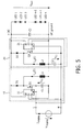
- Conduction loss of buck-boost rectifier diodes D1 and D2 can be reduced by realizing synchronous rectification with power semiconductors Q3, Q4 (here MOSFET transistors Q3, Q4, the source terminal of each of which is coupled to the drain terminal of the respective MOSFET transistor Q1, Q2), as depicted in Fig. 6 showing a circuit diagram of a second embodiment of the electronic driver circuit according to the present invention.
- the two control sub-units 12 and 22 require a slightly increased effort (half-bridge driver 37 rather than amplifier 34) and have two further control terminals f and g.
- the control terminal f is coupled to the drain terminal of the respective MOSFET transistor Q1, Q2 and the control terminal g is coupled to the gate terminal of the respective MOSFET transistor Q3, Q4.
- the circuits operate principally as follows.
- One of the two buck-boost converters 10, 20 operates as a synchronous mains rectifier and the other buck-boost converter operates as a buck-boost DC/DC converter.
- These two functions change after every zero crossing of the AC mains voltage V mains (t).
- the circuit detects the sign of the AC mains voltage, for which purpose - in these embodiments - control sub-units 11, 21 have control inputs a, b and c monitoring that.
- a sinusoidal AC mains voltage V mains having a frequency of e.g. 50 Hz as depicted in Fig. 7 will be considered.
- the AC mains voltage V mains is positive in the first half of the mains period (0 ⁇ t ⁇ 10 ms) and negative in the second period (10 ms ⁇ t ⁇ 20 ms).
- Control sub-unit 11 as shown in Fig. 14 , comprises a differential amplifier 30, a PI-type error amplifier 31, a pulse width modulator 32, an AND gate 33, an amplifier 34, a comparator and reference voltage unit 35 and an inverter 36.
- the control sub-unit 11 measures a small voltage between terminals b and a.
- Control sub-unit 11 measures further a negative voltage between terminals c and a.
- This comparator generates a logic high signal if the negative voltage -V ca (t) becomes larger than V ref.1 .
- This signal generates a voltage at terminal e of control sub-unit 11 that turns on MOSFET Q1 with a gate signal that is depicted in Fig. 10 .
- the turning-on of MOSFET transistor Q1 reduces the conduction loss in that device.
- the negative voltage -V ca (t) becomes smaller than V ref.1 and thus turns-off MOSFET transistor Q1.
- the output signal of comparator CO2 closes a switch S1 that short-circuits the input of the error amplifier 31.
- the voltage control loop of control sub-unit 11 is not active in this time interval.
- Control sub-unit 21 measures a positive voltage between terminals b and a in that first half-wave of the AC mains period.
- This comparator CO1 generates a logic high signal if the voltage V ba (t) becomes larger than V ref.1 .
- the control sub-unit 21 changes to the second operation mode to generate a regulated DC output voltage.
- Control sub-unit 21 generates gate signals at its terminal e depicted in Fig. 11 , that are conducted to MOSFET Q2 to operate buck-boost converter circuit 20 as a DC/DC converter.
- Current I L2 (t) ramps-up as depicted in Fig. 13 .
- MOSFET transistor Q2 Once MOSFET transistor Q2 is turned off, the current commutates from MOSFET transistor Q2 into rectifier diode D2 (in the embodiment shown in Fig. 5 ), or synchronous rectifier switch Q4 (in the embodiment shown in Fig. 6 ) to transfer the energy stored in inductor L2 into the output filter capacitor C3.
- Terminal d of control sub-unit 21 is used to measure output voltage V load as feedback signal for a voltage control loop that regulates the output voltage.
- V ba (t) V C2 (t) (shown in Fig. 9 ) drops below internal reference voltage level V ref1 .
- Comparator CO1 sends a logic low signal to a logic AND function A that turns-off the pulse-width modulated gate signals at output e of control sub-unit 21.
- both buck-boost converters 10, 20 change their functions.
- V C ⁇ 2 t - I mains t * j ⁇ 2 ⁇ ⁇ ⁇ f mains ⁇ L 2 + V SD Q ⁇ 2 .
- the maximum voltage on both capacitors C1 and C2 is the mains voltage amplitude that is more than two times lower than in the known embodiment shown above in Fig. 2 .
- the component voltage stress and internal power flow is greatly reduced compared with the control principle applied in this known embodiment.
- Figs. 5 and 6 generate a regulated DC output voltage by means of a voltage control loop.
- the stability of this voltage control loop can be improved by adding a peak current control loop to it.
- Fig. 16 shows a third embodiment of an electronic driver circuit that includes a peak current control loop. Both control sub-units 13, 23 have an additional input h to monitor the peak current in inductors L1 and L2.
- Fig. 17 shows a circuit diagram of control sub-units 13, 23.
- the peak current in inductors L1 and L2 as well as the energy flow in the electronic driver is regulated according to the time function of the AC mains voltage, resulting in an AC mains current with similar AC time function and high power factor.
- the circuits depicted in Figs. 5 , 6 and 16 generate a regulated average DC output voltage V load that is monitored at control sub-unit terminals b and d.
- the control of a regulated average DC current in a load can be achieved with additional measures, in particular an extended control function, as shown in a further embodiment of an electronic driver circuit shown in Fig. 18 .
- Both control sub-units 13, 23 are monitoring the DC current in the load LEDs by means of current shunt R3 at their control inputs b and d. This signal is compared with reference signal V ref.2 depicted in Fig. 17 and the output signal of that error amplifier is multiplied with the rectified mains voltage signal at control input b.
- That signal is a reference signal for the current control loop that turns-on MOSFET transistors Q1 or Q2 such that they generate always a peak current in inductors L1 or L2 that is twice the required AC mains current. That peak current is monitored by means of shunt resistors R1 and R2 at inputs h of control sub-units 13, 23. That control technique results in a high power factor of the AC mains current.
- Fig. 19 shows a circuit diagram of a still further embodiment of an electronic driver circuit according to the present invention.
- a single common control sub-unit 40 is provided for controlling both buck-boost converters 10, 20 instead of two separate control sub-units 11, 21.
- both function and control are generally identical.
- the present invention proposes an electronic driver circuit and its control principle for supplying electric loads such as LEDs and OLEDs in general and special lighting applications with a regulated DC current from AC mains, which driver circuit has a low component count and a high efficiency.
- the circuit comprises two buck-boost converters and operates according to a dedicated dual-mode principle to realize an AC/DC and DC/DC converter in a single conversion stage. This circuit is of special interest if a lamp driver is integrated in a LED or OLED system, and its high efficiency contributes to a low thermal stress of the system.
- control units and sub-units can, for example, be implemented in software, hardware or a mixture of software and hardware.
- the power semiconductors Q1 to Q4 and/or the diodes D1, D2 can also be implemented with other electronic components, e.g. other transistors or electronic circuits.
Claims (11)
- Circuit excitateur électronique pour alimenter une charge électronique (LED1, LED2,..., LEDn) en courant continu ou tension continue (Vload), comprenant :- une entrée de courant alternatif (L, N) pour recevoir une tension alternative d'entrée (Vmains),- deux convertisseurs dévolteurs-survolteurs (10, 20) pour fonctionner en alternance en tant que redresseur pour redresser ladite tension alternative d'entrée (Vmains) et en tant que convertisseur CC/CC pour la conversion de secteur CC de ladite tension alternative d'entrée redressée,- une unité de commande (11, 12, 13, 21, 22, 23 ; 40) pour surveiller le passage à zéro de la tension alternative d'entrée (Vmains) et pour commander lesdits deux convertisseurs dévolteurs-survolteurs (10, 20) pour changer leurs modes de fonctionnement lors de la détection d'un passage à zéro, de sorte que durant toutes les périodes un convertisseur dévolteur-survolteur sert de redresseur et l'autre convertisseur dévolteur-survolteur sert de convertisseur CC/CC.
- Circuit excitateur électronique selon la revendication 1, dans lequel ladite unité de commande (11, 12, 13, 21, 22, 23 ; 40) est adaptée pour surveiller le signe de ladite tension alternative d'entrée (Vmains).
- Circuit excitateur électronique selon la revendication 1, dans lequel au moins un desdits deux convertisseurs dévolteurs-survolteurs (10, 20) comprend un semi-conducteur de puissance (Q1, Q2), en particulier un transistor MOSFET, une diode de redressement (D1, D2) et une bobine d'induction de conversion (L1, L2).
- Circuit excitateur électronique selon la revendication 1, dans lequel au moins un desdits deux convertisseurs dévolteurs-survolteurs (10, 20) comprend un premier semi-conducteur de puissance (Q1, Q2), en particulier un premier transistor MOSFET, un second semi-conducteur de puissance (Q3, Q4), en particulier un second transistor MOSFET, et une bobine d'induction de conversion (L1, L2).
- Circuit excitateur électronique selon la revendication 1, dans lequel ladite unité de commande comprend une seule sous-unité de commande (40) pour surveiller le passage à zéro de la tension alternative d'entrée (Vmains) et commander le convertisseur dévolteur-survolteur respectif (10, 20) pour changer son mode de fonctionnement lors de la détection d'un passage à zéro.
- Circuit excitateur électronique selon la revendication 1, dans lequel ladite unité de commande comprend deux sous-unités de commande (11, 12, 13, 21, 22, 23), chacune étant incluse dans un desdits deux convertisseurs dévolteurs-survolteurs (10, 20) pour surveiller indépendamment le passage à zéro de la tension alternative d'entrée (Vmains) et commander le convertisseur dévolteur-survolteur respectif (10, 20) pour changer son mode de fonctionnement lors de la détection d'un passage à zéro.
- Circuit excitateur électronique selon la revendication 1, dans lequel ladite unité de commande (11, 12, 13, 21, 22, 23 ; 40) comporte une tension continue de référence interne (Vref.1) et deux comparateurs (CO1, CO2) pour allumer un semi-conducteur de puissance (Q1, Q2) en tant que semi-conducteur de puissance d'un convertisseur dévolteur-survolteur avec une sortie régulée et le second semi-conducteur de puissance en tant que redresseur synchrone.
- Circuit excitateur électronique selon la revendication 1, comprenant en outre une boucle de commande pour commander la tension continue (Vload) fournie à ladite charge (LED1, LED2, ... , LEDn), ladite boucle de commande comprenant :- deux bornes d'unité de commande pour surveiller ladite tension continue,- une tension continue de référence interne (Vref.2),- un amplificateur d'erreur pour comparer ladite tension continue surveillée et ladite tension continue de référence (Vref.2), et- un modulateur d'impulsions en durée (PWM) pour produire des impulsions et les fournir à un des deux semi-conducteurs de puissance (Q1, Q2) pour produire une tension de sortie régulée.
- Circuit excitateur électronique selon la revendication 1, dans lequel ladite unité de commande (13, 23) comprend une première boucle de commande pour commander la tension continue fournie à ladite charge électronique (LED1, LED2,..., LEDn) et une seconde boucle de commande pour commander le courant de crête dans des inducteurs dévolteurs-survolteurs (L1, L2), ladite boucle de commandes comprenant :- deux bornes d'entrée,- un amplificateur de différentiel pour mesurer la tension à la charge électronique,- une unité de surveillance (R1, R2) pour surveiller le courant de crête dans lesdits deux convertisseurs dévolteurs-survolteurs (10, 20), et- une unité de traitement pour comparer ladite tension continue surveillée à une seconde tension de référence interne (Vref.2), dans lequel le signal de sortie dudit amplificateur de différentiel est multiplié avec le signal de tension de secteur redressée à une entrée de commande pour produire un signal de référence pour une boucle de commande de courant qui régule le courant de crête dans les bobines d'induction des convertisseurs dévolteurs-survolteurs.
- Circuit excitateur électronique selon la revendication 6, dans lequel ladite unité de commande (13,23) comprend une boucle de commande pour commander le courant continu fourni à ladite charge électronique (LED1, LED2,..., LEDn), plus une seconde boucle de commande qui commande le courant de crête dans des inducteurs dévolteurs-survolteurs (L1, L2), ladite boucle de commande comprenant :- une première unité de surveillance (R3) pour surveiller le courant continu à ladite charge électronique (LED1, LED2,..., LEDn),- une seconde unité de surveillance (R1, R2) pour surveiller le courant de crête dans lesdits deux convertisseurs dévolteurs-survolteurs (10, 20), et- une unité de traitement (13, 23) pour comparer ledit courant continu surveillé à une seconde tension de référence interne (Vref.2), dans lequel le signal de sortie de cet amplificateur d'erreur est multiplié avec un signal de tension de secteur redressée à une entrée de commande pour produire un signal de référence pour une boucle de commande de courant qui régule le courant de crête dans les bobines d'induction des convertisseurs dévolteurs-survolteurs.
- Procédé d'excitation électronique d'alimentation d'une charge électronique (LED, LED2,..., LEDn) en courant continu ou tension continue (Vload), comprenant les étapes de :- la réception d'une tension alternative d'entrée (Vmains),- le redressement de ladite tension alternative d'entrée (Vmains) par un premier de deux convertisseurs dévolteurs-survolteurs (10, 20),- la conversion en courant continu de ladite tension alternative d'entrée redressée par le second desdits deux convertisseurs dévolteurs-survolteurs (10, 20),- la surveillance du passage à zéro de la tension alternative d'entrée (Vmains), et- la commande desdits deux convertisseurs dévolteurs-survolteurs (10, 20) pour changer leurs modes de fonctionnement lors de la détection d'un passage à zéro, de sorte que durant toutes les périodes un convertisseur dévolteur-survolteur sert de redresseur et l'autre convertisseur dévolteur-survolteur sert de convertisseur CC/CC.
Priority Applications (1)
| Application Number | Priority Date | Filing Date | Title |
|---|---|---|---|
| EP09706501.5A EP2248249B1 (fr) | 2008-01-29 | 2009-01-26 | Circuit d'attaque électronique et procédé |
Applications Claiming Priority (3)
| Application Number | Priority Date | Filing Date | Title |
|---|---|---|---|
| EP08101059 | 2008-01-29 | ||
| PCT/IB2009/050299 WO2009095836A2 (fr) | 2008-01-29 | 2009-01-26 | Circuit d'attaque électronique et procédé |
| EP09706501.5A EP2248249B1 (fr) | 2008-01-29 | 2009-01-26 | Circuit d'attaque électronique et procédé |
Publications (2)
| Publication Number | Publication Date |
|---|---|
| EP2248249A2 EP2248249A2 (fr) | 2010-11-10 |
| EP2248249B1 true EP2248249B1 (fr) | 2013-08-28 |
Family
ID=40801981
Family Applications (1)
| Application Number | Title | Priority Date | Filing Date |
|---|---|---|---|
| EP09706501.5A Not-in-force EP2248249B1 (fr) | 2008-01-29 | 2009-01-26 | Circuit d'attaque électronique et procédé |
Country Status (7)
| Country | Link |
|---|---|
| US (1) | US8355268B2 (fr) |
| EP (1) | EP2248249B1 (fr) |
| JP (1) | JP5117580B2 (fr) |
| KR (1) | KR20100113603A (fr) |
| CN (1) | CN101926082B (fr) |
| TW (1) | TW200942076A (fr) |
| WO (1) | WO2009095836A2 (fr) |
Families Citing this family (23)
| Publication number | Priority date | Publication date | Assignee | Title |
|---|---|---|---|---|
| TWI382626B (zh) * | 2009-10-09 | 2013-01-11 | Foxsemicon Integrated Tech Inc | 放電電路 |
| US8553439B2 (en) | 2010-02-09 | 2013-10-08 | Power Integrations, Inc. | Method and apparatus for determining zero-crossing of an AC input voltage to a power supply |
| US8299730B2 (en) | 2010-02-09 | 2012-10-30 | Power Integrations, Inc. | Integrated on-time extension for non-dissipative bleeding in a power supply |
| US8237371B2 (en) * | 2010-10-29 | 2012-08-07 | O2 Micro, Inc | Differential driving circuit for powering a light source |
| US20130307523A1 (en) * | 2011-02-03 | 2013-11-21 | Mitsubishi Electric Corporation | Analog unit of sequencer system |
| EP2719063B1 (fr) | 2011-06-10 | 2018-08-08 | Philips Lighting Holding B.V. | Dispositif de commande cc/cc muni de filtres d'entrée et de sortie pour la commande d'une charge, en particulier d'une unité led |
| WO2012172459A1 (fr) | 2011-06-17 | 2012-12-20 | Koninklijke Philips Electronics N.V. | Dispositif de commande cc/cc muni de filtres d'entrée et de sortie pour la commande d'une charge, en particulier d'une unité led |
| JP5678860B2 (ja) * | 2011-10-07 | 2015-03-04 | 株式会社安川電機 | 交流直流変換器 |
| KR101876455B1 (ko) | 2011-11-07 | 2018-07-11 | 삼성디스플레이 주식회사 | Dc-dc 컨버터 및 이를 포함하는 발광 다이오드 구동 장치 |
| CN102573235B (zh) * | 2012-01-11 | 2013-07-24 | 矽力杰半导体技术(杭州)有限公司 | 一种高效率的led驱动电路及其驱动方法 |
| US20130193865A1 (en) * | 2012-01-26 | 2013-08-01 | Joseph Rudy Keller | Method and apparatus for driving a light emitting diode strobe |
| CN104321959A (zh) | 2012-03-20 | 2015-01-28 | 印第安纳大学研究与技术公司 | 单开关无限级电力逆变器 |
| CN103427633A (zh) * | 2012-05-15 | 2013-12-04 | 通用电气公司 | 高压应用的开关模式功率转换器 |
| US10971894B2 (en) | 2015-06-22 | 2021-04-06 | Maxim Integrated Products, Inc. | Driver for high speed laser diode |
| US9426854B1 (en) * | 2015-11-30 | 2016-08-23 | General Electric Company | Electronic driver for controlling an illumination device |
| US9420656B1 (en) * | 2015-12-15 | 2016-08-16 | Tong Xin Technology Co., Ltd. | Light emitting diode dimmer circuit |
| US9825552B1 (en) * | 2016-09-13 | 2017-11-21 | Kabushiki Kaisha Toshiba | Power conversion apparatus |
| CN107546965A (zh) * | 2017-09-26 | 2018-01-05 | 广东工业大学 | 一种交直流混合的四端口电力电子变压器 |
| US10797660B2 (en) | 2018-04-16 | 2020-10-06 | Maxim Integrated Products, Inc. | Multiphase buck-boost amplifier |
| GB2573318B (en) * | 2018-05-03 | 2020-06-10 | Zhong Qingchang | SYNDEM converter |
| US11145242B2 (en) * | 2019-10-29 | 2021-10-12 | Facebook Technologies, Llc | Apparatus, system, and method for efficiently driving visual displays via light-emitting devices |
| RU2739704C1 (ru) * | 2020-09-29 | 2020-12-28 | Дмитрий Николаевич Карпенко | Устройство и система модульного равномерного освещения |
| US11922892B2 (en) | 2021-01-20 | 2024-03-05 | Meta Platforms Technologies, Llc | High-efficiency backlight driver |
Family Cites Families (10)
| Publication number | Priority date | Publication date | Assignee | Title |
|---|---|---|---|---|
| FR2729516B1 (fr) * | 1995-01-13 | 1997-04-18 | Sextant Avionique | Convertisseurs de tension bidirectionnels de type continu-continu et capteur de courant |
| JP2000270564A (ja) * | 1999-03-15 | 2000-09-29 | Mitsubishi Electric Corp | 連系装置 |
| US6320772B1 (en) * | 1999-05-26 | 2001-11-20 | Matsushita Electric Industrial Co., Ltd. | Converter circuit having control means with capability to short-circuit converter output |
| DE10004024A1 (de) | 2000-01-31 | 2001-08-02 | Guenther Bebenroth | Schaltungsanordnung zum Betreiben von Leuchtdioden |
| EP1211791B1 (fr) | 2000-12-04 | 2011-02-16 | Nec Tokin Corporation | Convertisseur continu-continu symétrique avec des redresseurs synchrone pilotées à l'aide des amplificateurs opérationnels |
| JP2004173421A (ja) * | 2002-11-20 | 2004-06-17 | Matsushita Electric Ind Co Ltd | Dc/dcコンバータ |
| US20060198172A1 (en) * | 2003-10-01 | 2006-09-07 | International Rectifier Corporation | Bridgeless boost converter with PFC circuit |
| CN1906837B (zh) * | 2004-03-18 | 2011-02-23 | 三井物产株式会社 | 直流-直流转换器 |
| US7269038B2 (en) * | 2005-09-12 | 2007-09-11 | Fairchild Semiconductor Corporation | Vrms and rectified current sense full-bridge synchronous-rectification integrated with PFC |
| US7518895B2 (en) * | 2006-06-30 | 2009-04-14 | Fairchild Semiconductor Corporation | High-efficiency power converter system |
-
2009
- 2009-01-26 WO PCT/IB2009/050299 patent/WO2009095836A2/fr active Application Filing
- 2009-01-26 CN CN2009801032844A patent/CN101926082B/zh not_active Expired - Fee Related
- 2009-01-26 EP EP09706501.5A patent/EP2248249B1/fr not_active Not-in-force
- 2009-01-26 JP JP2010543617A patent/JP5117580B2/ja not_active Expired - Fee Related
- 2009-01-26 KR KR1020107019184A patent/KR20100113603A/ko not_active Application Discontinuation
- 2009-01-26 US US12/863,991 patent/US8355268B2/en not_active Expired - Fee Related
- 2009-02-02 TW TW098103276A patent/TW200942076A/zh unknown
Also Published As
| Publication number | Publication date |
|---|---|
| US8355268B2 (en) | 2013-01-15 |
| KR20100113603A (ko) | 2010-10-21 |
| WO2009095836A3 (fr) | 2009-10-15 |
| TW200942076A (en) | 2009-10-01 |
| CN101926082B (zh) | 2013-09-04 |
| WO2009095836A2 (fr) | 2009-08-06 |
| CN101926082A (zh) | 2010-12-22 |
| EP2248249A2 (fr) | 2010-11-10 |
| JP5117580B2 (ja) | 2013-01-16 |
| US20100296324A1 (en) | 2010-11-25 |
| JP2011511607A (ja) | 2011-04-07 |
Similar Documents
| Publication | Publication Date | Title |
|---|---|---|
| EP2248249B1 (fr) | Circuit d'attaque électronique et procédé | |
| Lee et al. | A single-switch AC–DC LED driver based on a boost-flyback PFC converter with lossless snubber | |
| Zhang et al. | A precise passive current balancing method for multioutput LED drivers | |
| EP2536013B1 (fr) | Convertisseur élévateur et abaisseur dans une configuration cascade | |
| CN102801341B (zh) | 具有pfc和dc/dc转换器的ac/dc转换器 | |
| US9148072B2 (en) | Inverter apparatus | |
| US8710757B2 (en) | Power converter for an LED assembly and lighting application | |
| TWI475793B (zh) | 使用具整流切換開關之z型轉換器將交流輸入電壓轉換為調整的直流輸出電壓的轉換器、電子裝置與方法 | |
| US20100259240A1 (en) | Bridgeless PFC converter | |
| US7751212B2 (en) | Methods and apparatus for three-phase rectifier with lower voltage switches | |
| US20120293141A1 (en) | Bridgeless pfc converter and the method thereof | |
| CN202652596U (zh) | 用于控制一个或更多个发光二极管的调光级别的电路 | |
| US8901832B2 (en) | LED driver system with dimmer detection | |
| US8773875B2 (en) | Power conversion apparatus | |
| WO2015135073A1 (fr) | Attaque de del commandée par le côté primaire avec annulation d'ondulation | |
| CN105305805A (zh) | 功率因数修正装置 | |
| Wang et al. | A family of capacitive current balancing methods for multi-output LED drivers | |
| US10143046B2 (en) | Light emitting diode driver with differential voltage supply | |
| US9369050B1 (en) | Indirect current sensing method for a constant current flyback converter | |
| Pandey et al. | An AC LED driver with improved total harmonic distortion and power factor | |
| KR100420964B1 (ko) | 역률보상 단일단 컨버터 | |
| KR20180004677A (ko) | 브릿지리스 인터리브 역률보정회로 및 그 구동방법 | |
| Şehirli et al. | Comparison of single phase buck-boost and sepic LED driver | |
| WO2010041169A1 (fr) | Circuit de commande ca/cc triphasé, pour des led par exemple | |
| US9318959B2 (en) | Low total harmonic distortion and high power factor correction power converters |
Legal Events
| Date | Code | Title | Description |
|---|---|---|---|
| PUAI | Public reference made under article 153(3) epc to a published international application that has entered the european phase |
Free format text: ORIGINAL CODE: 0009012 |
|
| 17P | Request for examination filed |
Effective date: 20100830 |
|
| AK | Designated contracting states |
Kind code of ref document: A2 Designated state(s): AT BE BG CH CY CZ DE DK EE ES FI FR GB GR HR HU IE IS IT LI LT LU LV MC MK MT NL NO PL PT RO SE SI SK TR |
|
| AX | Request for extension of the european patent |
Extension state: AL BA RS |
|
| DAX | Request for extension of the european patent (deleted) | ||
| GRAP | Despatch of communication of intention to grant a patent |
Free format text: ORIGINAL CODE: EPIDOSNIGR1 |
|
| INTG | Intention to grant announced |
Effective date: 20130403 |
|
| GRAS | Grant fee paid |
Free format text: ORIGINAL CODE: EPIDOSNIGR3 |
|
| GRAA | (expected) grant |
Free format text: ORIGINAL CODE: 0009210 |
|
| AK | Designated contracting states |
Kind code of ref document: B1 Designated state(s): AT BE BG CH CY CZ DE DK EE ES FI FR GB GR HR HU IE IS IT LI LT LU LV MC MK MT NL NO PL PT RO SE SI SK TR |
|
| REG | Reference to a national code |
Ref country code: GB Ref legal event code: FG4D |
|
| REG | Reference to a national code |
Ref country code: CH Ref legal event code: EP |
|
| REG | Reference to a national code |
Ref country code: AT Ref legal event code: REF Ref document number: 629798 Country of ref document: AT Kind code of ref document: T Effective date: 20130915 |
|
| RAP2 | Party data changed (patent owner data changed or rights of a patent transferred) |
Owner name: PHILIPS INTELLECTUAL PROPERTY & STANDARDS GMBH Owner name: KONINKLIJKE PHILIPS N.V. |
|
| REG | Reference to a national code |
Ref country code: IE Ref legal event code: FG4D |
|
| REG | Reference to a national code |
Ref country code: DE Ref legal event code: R096 Ref document number: 602009018351 Country of ref document: DE Effective date: 20131024 |
|
| REG | Reference to a national code |
Ref country code: AT Ref legal event code: MK05 Ref document number: 629798 Country of ref document: AT Kind code of ref document: T Effective date: 20130828 |
|
| REG | Reference to a national code |
Ref country code: LT Ref legal event code: MG4D |
|
| REG | Reference to a national code |
Ref country code: NL Ref legal event code: VDEP Effective date: 20130828 |
|
| PG25 | Lapsed in a contracting state [announced via postgrant information from national office to epo] |
Ref country code: HR Free format text: LAPSE BECAUSE OF FAILURE TO SUBMIT A TRANSLATION OF THE DESCRIPTION OR TO PAY THE FEE WITHIN THE PRESCRIBED TIME-LIMIT Effective date: 20130828 Ref country code: IS Free format text: LAPSE BECAUSE OF FAILURE TO SUBMIT A TRANSLATION OF THE DESCRIPTION OR TO PAY THE FEE WITHIN THE PRESCRIBED TIME-LIMIT Effective date: 20131228 Ref country code: NO Free format text: LAPSE BECAUSE OF FAILURE TO SUBMIT A TRANSLATION OF THE DESCRIPTION OR TO PAY THE FEE WITHIN THE PRESCRIBED TIME-LIMIT Effective date: 20131128 Ref country code: SE Free format text: LAPSE BECAUSE OF FAILURE TO SUBMIT A TRANSLATION OF THE DESCRIPTION OR TO PAY THE FEE WITHIN THE PRESCRIBED TIME-LIMIT Effective date: 20130828 Ref country code: PT Free format text: LAPSE BECAUSE OF FAILURE TO SUBMIT A TRANSLATION OF THE DESCRIPTION OR TO PAY THE FEE WITHIN THE PRESCRIBED TIME-LIMIT Effective date: 20131230 Ref country code: AT Free format text: LAPSE BECAUSE OF FAILURE TO SUBMIT A TRANSLATION OF THE DESCRIPTION OR TO PAY THE FEE WITHIN THE PRESCRIBED TIME-LIMIT Effective date: 20130828 Ref country code: LT Free format text: LAPSE BECAUSE OF FAILURE TO SUBMIT A TRANSLATION OF THE DESCRIPTION OR TO PAY THE FEE WITHIN THE PRESCRIBED TIME-LIMIT Effective date: 20130828 Ref country code: CY Free format text: LAPSE BECAUSE OF FAILURE TO SUBMIT A TRANSLATION OF THE DESCRIPTION OR TO PAY THE FEE WITHIN THE PRESCRIBED TIME-LIMIT Effective date: 20130911 |
|
| REG | Reference to a national code |
Ref country code: NL Ref legal event code: VDEP Effective date: 20130828 |
|
| PG25 | Lapsed in a contracting state [announced via postgrant information from national office to epo] |
Ref country code: BE Free format text: LAPSE BECAUSE OF FAILURE TO SUBMIT A TRANSLATION OF THE DESCRIPTION OR TO PAY THE FEE WITHIN THE PRESCRIBED TIME-LIMIT Effective date: 20130828 Ref country code: LV Free format text: LAPSE BECAUSE OF FAILURE TO SUBMIT A TRANSLATION OF THE DESCRIPTION OR TO PAY THE FEE WITHIN THE PRESCRIBED TIME-LIMIT Effective date: 20130828 Ref country code: SI Free format text: LAPSE BECAUSE OF FAILURE TO SUBMIT A TRANSLATION OF THE DESCRIPTION OR TO PAY THE FEE WITHIN THE PRESCRIBED TIME-LIMIT Effective date: 20130828 Ref country code: PL Free format text: LAPSE BECAUSE OF FAILURE TO SUBMIT A TRANSLATION OF THE DESCRIPTION OR TO PAY THE FEE WITHIN THE PRESCRIBED TIME-LIMIT Effective date: 20130828 Ref country code: FI Free format text: LAPSE BECAUSE OF FAILURE TO SUBMIT A TRANSLATION OF THE DESCRIPTION OR TO PAY THE FEE WITHIN THE PRESCRIBED TIME-LIMIT Effective date: 20130828 Ref country code: GR Free format text: LAPSE BECAUSE OF FAILURE TO SUBMIT A TRANSLATION OF THE DESCRIPTION OR TO PAY THE FEE WITHIN THE PRESCRIBED TIME-LIMIT Effective date: 20131129 |
|
| PG25 | Lapsed in a contracting state [announced via postgrant information from national office to epo] |
Ref country code: CY Free format text: LAPSE BECAUSE OF FAILURE TO SUBMIT A TRANSLATION OF THE DESCRIPTION OR TO PAY THE FEE WITHIN THE PRESCRIBED TIME-LIMIT Effective date: 20130828 |
|
| PG25 | Lapsed in a contracting state [announced via postgrant information from national office to epo] |
Ref country code: NL Free format text: LAPSE BECAUSE OF FAILURE TO SUBMIT A TRANSLATION OF THE DESCRIPTION OR TO PAY THE FEE WITHIN THE PRESCRIBED TIME-LIMIT Effective date: 20130828 Ref country code: CZ Free format text: LAPSE BECAUSE OF FAILURE TO SUBMIT A TRANSLATION OF THE DESCRIPTION OR TO PAY THE FEE WITHIN THE PRESCRIBED TIME-LIMIT Effective date: 20130828 Ref country code: EE Free format text: LAPSE BECAUSE OF FAILURE TO SUBMIT A TRANSLATION OF THE DESCRIPTION OR TO PAY THE FEE WITHIN THE PRESCRIBED TIME-LIMIT Effective date: 20130828 Ref country code: SK Free format text: LAPSE BECAUSE OF FAILURE TO SUBMIT A TRANSLATION OF THE DESCRIPTION OR TO PAY THE FEE WITHIN THE PRESCRIBED TIME-LIMIT Effective date: 20130828 Ref country code: DK Free format text: LAPSE BECAUSE OF FAILURE TO SUBMIT A TRANSLATION OF THE DESCRIPTION OR TO PAY THE FEE WITHIN THE PRESCRIBED TIME-LIMIT Effective date: 20130828 Ref country code: RO Free format text: LAPSE BECAUSE OF FAILURE TO SUBMIT A TRANSLATION OF THE DESCRIPTION OR TO PAY THE FEE WITHIN THE PRESCRIBED TIME-LIMIT Effective date: 20130828 |
|
| PG25 | Lapsed in a contracting state [announced via postgrant information from national office to epo] |
Ref country code: IT Free format text: LAPSE BECAUSE OF FAILURE TO SUBMIT A TRANSLATION OF THE DESCRIPTION OR TO PAY THE FEE WITHIN THE PRESCRIBED TIME-LIMIT Effective date: 20130828 Ref country code: ES Free format text: LAPSE BECAUSE OF FAILURE TO SUBMIT A TRANSLATION OF THE DESCRIPTION OR TO PAY THE FEE WITHIN THE PRESCRIBED TIME-LIMIT Effective date: 20130828 |
|
| PGFP | Annual fee paid to national office [announced via postgrant information from national office to epo] |
Ref country code: FR Payment date: 20140129 Year of fee payment: 6 |
|
| REG | Reference to a national code |
Ref country code: DE Ref legal event code: R097 Ref document number: 602009018351 Country of ref document: DE |
|
| PGFP | Annual fee paid to national office [announced via postgrant information from national office to epo] |
Ref country code: GB Payment date: 20140131 Year of fee payment: 6 |
|
| PLBE | No opposition filed within time limit |
Free format text: ORIGINAL CODE: 0009261 |
|
| STAA | Information on the status of an ep patent application or granted ep patent |
Free format text: STATUS: NO OPPOSITION FILED WITHIN TIME LIMIT |
|
| 26N | No opposition filed |
Effective date: 20140530 |
|
| PG25 | Lapsed in a contracting state [announced via postgrant information from national office to epo] |
Ref country code: LU Free format text: LAPSE BECAUSE OF FAILURE TO SUBMIT A TRANSLATION OF THE DESCRIPTION OR TO PAY THE FEE WITHIN THE PRESCRIBED TIME-LIMIT Effective date: 20140126 Ref country code: MC Free format text: LAPSE BECAUSE OF FAILURE TO SUBMIT A TRANSLATION OF THE DESCRIPTION OR TO PAY THE FEE WITHIN THE PRESCRIBED TIME-LIMIT Effective date: 20130828 |
|
| PGFP | Annual fee paid to national office [announced via postgrant information from national office to epo] |
Ref country code: DE Payment date: 20140331 Year of fee payment: 6 |
|
| REG | Reference to a national code |
Ref country code: CH Ref legal event code: PL |
|
| REG | Reference to a national code |
Ref country code: DE Ref legal event code: R097 Ref document number: 602009018351 Country of ref document: DE Effective date: 20140530 |
|
| PG25 | Lapsed in a contracting state [announced via postgrant information from national office to epo] |
Ref country code: LI Free format text: LAPSE BECAUSE OF NON-PAYMENT OF DUE FEES Effective date: 20140131 Ref country code: CH Free format text: LAPSE BECAUSE OF NON-PAYMENT OF DUE FEES Effective date: 20140131 |
|
| REG | Reference to a national code |
Ref country code: IE Ref legal event code: MM4A |
|
| PG25 | Lapsed in a contracting state [announced via postgrant information from national office to epo] |
Ref country code: IE Free format text: LAPSE BECAUSE OF NON-PAYMENT OF DUE FEES Effective date: 20140126 |
|
| REG | Reference to a national code |
Ref country code: DE Ref legal event code: R119 Ref document number: 602009018351 Country of ref document: DE |
|
| GBPC | Gb: european patent ceased through non-payment of renewal fee |
Effective date: 20150126 |
|
| PG25 | Lapsed in a contracting state [announced via postgrant information from national office to epo] |
Ref country code: GB Free format text: LAPSE BECAUSE OF NON-PAYMENT OF DUE FEES Effective date: 20150126 Ref country code: DE Free format text: LAPSE BECAUSE OF NON-PAYMENT OF DUE FEES Effective date: 20150801 |
|
| REG | Reference to a national code |
Ref country code: FR Ref legal event code: ST Effective date: 20150930 |
|
| PG25 | Lapsed in a contracting state [announced via postgrant information from national office to epo] |
Ref country code: FR Free format text: LAPSE BECAUSE OF NON-PAYMENT OF DUE FEES Effective date: 20150202 |
|
| PG25 | Lapsed in a contracting state [announced via postgrant information from national office to epo] |
Ref country code: MT Free format text: LAPSE BECAUSE OF FAILURE TO SUBMIT A TRANSLATION OF THE DESCRIPTION OR TO PAY THE FEE WITHIN THE PRESCRIBED TIME-LIMIT Effective date: 20130828 |
|
| PG25 | Lapsed in a contracting state [announced via postgrant information from national office to epo] |
Ref country code: BG Free format text: LAPSE BECAUSE OF FAILURE TO SUBMIT A TRANSLATION OF THE DESCRIPTION OR TO PAY THE FEE WITHIN THE PRESCRIBED TIME-LIMIT Effective date: 20130828 |
|
| PG25 | Lapsed in a contracting state [announced via postgrant information from national office to epo] |
Ref country code: TR Free format text: LAPSE BECAUSE OF FAILURE TO SUBMIT A TRANSLATION OF THE DESCRIPTION OR TO PAY THE FEE WITHIN THE PRESCRIBED TIME-LIMIT Effective date: 20130828 Ref country code: HU Free format text: LAPSE BECAUSE OF FAILURE TO SUBMIT A TRANSLATION OF THE DESCRIPTION OR TO PAY THE FEE WITHIN THE PRESCRIBED TIME-LIMIT; INVALID AB INITIO Effective date: 20090126 |
|
| PG25 | Lapsed in a contracting state [announced via postgrant information from national office to epo] |
Ref country code: MK Free format text: LAPSE BECAUSE OF FAILURE TO SUBMIT A TRANSLATION OF THE DESCRIPTION OR TO PAY THE FEE WITHIN THE PRESCRIBED TIME-LIMIT Effective date: 20130828 |