EP2246784A1 - Programmaktualisierungssystem und elektronisches Gerät mit Programmaktualisierungsfunktion - Google Patents
Programmaktualisierungssystem und elektronisches Gerät mit Programmaktualisierungsfunktion Download PDFInfo
- Publication number
- EP2246784A1 EP2246784A1 EP10004437A EP10004437A EP2246784A1 EP 2246784 A1 EP2246784 A1 EP 2246784A1 EP 10004437 A EP10004437 A EP 10004437A EP 10004437 A EP10004437 A EP 10004437A EP 2246784 A1 EP2246784 A1 EP 2246784A1
- Authority
- EP
- European Patent Office
- Prior art keywords
- program
- cpu
- correction
- address
- update
- Prior art date
- Legal status (The legal status is an assumption and is not a legal conclusion. Google has not performed a legal analysis and makes no representation as to the accuracy of the status listed.)
- Withdrawn
Links
Images

Classifications
-
- G—PHYSICS
- G06—COMPUTING OR CALCULATING; COUNTING
- G06F—ELECTRIC DIGITAL DATA PROCESSING
- G06F8/00—Arrangements for software engineering
- G06F8/60—Software deployment
- G06F8/65—Updates
Definitions
- This invention relates to a program update system and an electronic device with program update function. More specifically, this invention relates to a system and an electronic device provided with function to update (version up) a control program used to decode compressed data that is taken-in from a USB (Universal Serial Bus) memory or the like.
- a USB Universal Serial Bus
- an electronic devices such as a car audio takes-in compressed data stored in an external recording medium such as a USB memory or iPod (iPod is a registered trade mark of Apple Incorporated).
- Standardized audio file formats such as MP3, WMA and AAC are used as a format of the compressed data.
- the compressed data is decoded by a compression decoder in the electronic device and then played back as a sound through a speaker or the like.
- a microcomputer having a USB host function executes a control program of the compression decoder.
- a flash ROM an electrically erasable programmable nonvolatile memory, hereafter referred to as an FROM
- the control program is revised using the FROM.
- control program corresponding to the USB memories available in the market at the time of the shipping of the electronic device is written into the FROM in the electronic device.
- update information for the control program is written into the new USB memory.
- the control program is revised (updated) by writing the update information into the FROM.
- the compression decoder and the microcomputer itself that includes a CPU, a RAM and the like, do not need the FROM process in themselves, they have to be manufactured using the FROM process in order to be integrated in the single chip together with the FROM.
- the FROM process is not suitable for finer design rules required to reduce the size of devices in the single chip, because the FROM process requires a larger number of masks and an increased amount of thermal treatment compared with a logic process that is used to manufacture logic circuits. As a result, the single chip is increased in its die size as well as its manufacturing cost.
- the invention provides an integrated circuit chip with program update functions.
- the chip includes an interface circuit interfacing with an external recording medium, a compression decoder decoding compressed data received from the external recording medium through the interface circuit, a mask ROM storing a program to control the compression decoder, and a CPU executing the program stored in the mask ROM.
- the mask ROM and the CPU are configured to operate as part of a ROM correction circuit correcting the program stored in the mask ROM based on update information of the program stored in the external recording medium.
- the integrated circuit chip is configured to transmit data to and receive data from an electrically erasable programmable nonvolatile memory external to the integrated circuit chip and is configured to write the update information received from the external recording medium through the interface circuit into the nonvolatile memory.
- the ROM correction circuit is configured to update the program stored in the mask ROM when the CPU executes the program.
- the invention also provides an electronic device with program update functions.
- the device includes a first integrated circuit chip having an interface circuit interfacing with an external recording medium, a compression decoder decoding compressed data received from the external recording medium through the interface circuit, a mask ROM storing a first program to control the compression decoder, and a first CPU executing the first program stored in the mask ROM.
- the mask ROM and the first CPU operate as part of a ROM correction circuit correcting the first program stored in the mask ROM based on update information of the first program stored in the external recording medium.
- the device also includes a second integrated circuit chip having an electrically erasable programmable nonvolatile memory and a second CPU executing a second program stored in the nonvolatile memory and controlling the electronic device.
- the first integrated circuit chip is configured to transmit data to and receive data from the second integrated circuit chip and is configured to write the update information received from the external recording medium through the interface circuit into the nonvolatile memory.
- the ROM correction circuit is configured to update the first program stored in the mask ROM when the first CPU executes the first program.
- a program update system and an electronic device with a program update function according to an embodiment of this invention are described referring to the drawings.
- a car audio is taken as an example of the electronic device and is explained hereafter.
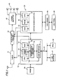
- a first integrated circuit chip 10 has a USB interface circuit 11, a compression decoder 12, a CPU 13, a mask ROM (Read Only Memory) 14 and a RAM (Random Access Memory) 15.
- the first integrated circuit chip 10 is a single chip consolidating a microcomputer with a USB host function and the compression decoder 12. It should be noted that the first integrated circuit chip 10 incorporates the mask ROM 14, not an FROM, as a memory to store a control program (before update) to control an operation of the compression decoder 12.
- the mask ROM 14 is a nonvolatile read-only memory, and its ROM coding is modified by modifying an ion implantation mask, a metal mask, a contact mask or the like. It is manufactured using a less expensive process and suitable for finer design rules compared with the FROM.
- the RAM 15 is a memory to store data temporarily. The data stored in the RAM 15 is lost when a power supply is turned off.
- the USB interface circuit 11 serves to interface the first integrated circuit chip 10 and the external recording medium such as the USB memory 31 or the iPod 32, and has a function to convert serial data transferred from the USB memory 31 into a data format that can be processed in the first integrated circuit chip 10, for example, that is, a function to convert the serial data from the USB memory 31 into parallel data, for example.
- the USB memory 31, the iPod 32 or the like is connected to the USB interface circuit 11 through a USB cable 33.
- the compression decoder 12 decodes the compression date (in the format of MP3, WMA, AAC or the like in this case) inputted from the USB memory 31 or the like through the USB interface circuit 11.
- the USB interface circuit 11, the compression decoder 12, the CPU 13, the mask ROM 14 and the RAM 15 are configured so that they can transmit/receive the data or the like to/from each other through a bus 16.
- a DRAM 34 is provided outside the first integrated circuit chip 10. The DRAM 34 can be used as a buffer memory to store the data transferred from the USB interface circuit 11 collectively.
- a second integrated circuit chip 20 is a semiconductor chip separated from the first integrated circuit chip 10. It has a CPU 21, an FROM 22 and a RAM 23, and serves as a system microcomputer to control the whole system of the car audio.
- the CPU 21, the FROM 22 and the RAM 23 are configured so that they can transmit/receive the data or the like to/from each other through a bus 24.
- the second integrated circuit chip 20 controls operations of a tuner 41, an electronic volume 42, a power amplifier 43 and an LCD driver 44.
- the second integrated circuit chip 20 sends a display signal and a display instruction to the LCD driver 44.
- the LCD driver 44 drives an LCD panel 46 in accordance with them.
- a predetermined LCD display is performed as a result.
- An audio signal decoded by the compression decoder 12 is inputted to the electronic volume 42 and its sound volume is adjusted based on the instruction from the second integrated circuit chip 20.
- the audio signal with the sound volume adjusted by the electronic volume 42 is amplified by the power amplifier 43.
- the audio signal amplified by the power amplifier 43 is played back as a sound through a speaker 45.
- USB memory 31 When the USB memory 31 is connected to the USB interface circuit 11 through the cable 33, data communication in compliance with a USB communication protocol takes place between the USB memory 31 and the USB interface circuit 11. That is, the first integrated circuit chip 10 recognizes that the USB memory 31 is connected and sets up a state in which the update information and the compressed data can be transferred from the USB memory 31 to the USB interface circuit 11.
- the update information stored in the USB memory 31 is written into the FROM 22 in the second integrated circuit chip 20 through the interface circuit 11.
- the update information inputted through the USB interface circuit 11 may be temporarily stored in the DRAM 34 that serves as the buffer memory. By doing so, the time required to transfer the update information from the first integrated circuit chip 10 to the FROM 22 can be reduced because the update information stored in the DRAM 34 can be collectively transferred to the FROM 22.
- the CPU 13 takes-in the compressed data stored in the USB memory 31 through the USB interface circuit 11 and converts into the data format that can be processed by the compression decoder 12 by executing the control program.
- the converted compressed data is transferred to the compression decoder 12 and decoded.
- the control program stored in the mask ROM is automatically updated when the CPU 13 executes the control program. That is, the update information written into the FROM 22 is transferred to the first integrated circuit chip 10 and the program stored in the mask ROM 14 is updated with a ROM correction function of the first integrated circuit chip 10. At that time, the update information written into the FROM 22 may be temporarily stored in the RAM 23 in the second integrated circuit chip 20. By doing so, the update information stored in the RAM 23 can be transferred to the first integrated circuit chip 10 collectively.
- the first integrated circuit chip 10 does not include the FROM, the single chip consolidating the microcomputer with the USB host function and the compression decoder 12 can be manufactured using the less expensive logic process.
- the second integrated circuit chip 20, that is the system microcomputer, includes the FROM 22 in order to reduce a lead time and expedite debugging of the program.
- control program stored in the mask ROM 14 is updated using the FROM 22 incorporated in the system microcomputer.
- the update information written into the FROM 22 in the second integrated circuit chip 20 is transferred to the RAM 15 in the first integrated circuit chip 10, and the data outputted from the mask ROM 14 is corrected (replaced) based on the update information that is temporarily stored in the RAM 15.
- update information and the compressed data are downloaded from the USB memory 31 in the embodiment described above, the information and the data may be downloaded from other external recording medium such as the iPod 32 or an SD card.
- the ROM correction circuit is composed of the CPU 13, the mask ROM 14, the RAM 15 (an example of "retaining circuit") and a selection circuit (multiplexer) 17.
- the update information of the control program includes correction address (data) that indicates an address in the control program to be corrected (that is, a location in the original control program to be corrected) and correction data corresponding the correction address.
- the correction address and the correction data are written into the FROM 22 in the second integrated circuit chip 20 as described above.
- the correction address and the correction data stored in the FROM 22 are transferred to the RAM 15 in the first integrated circuit chip 10 and temporarily retained in it.
- the CPU 13 incorporates a program counter that sequentially outputs addresses to access the mask ROM 14.
- the mask ROM 14 outputs a program data (ROM code) corresponding to the address outputted from the CPU 13.
- the CPU outputs the address not only to the mask ROM 14 but also to the RAM 15.
- the selection circuit 17 outputs the correction data when the address outputted from the CPU 13 coincides with the address retained in the RAM 15. When the address outputted from the CPU 13 does no coincide with the address retained in the RAM 15, the selection circuit 17 outputs the program data stored in the mask ROM 14 at the corresponding address.
- Detection of the coincidence between the address outputted from the CPU 13 and the correction address may be carried out using arithmetic function (ALU) of the CPU 13, or may be made by a coincidence detection circuit provided in a form of hardware.
- ALU arithmetic function
- the selection circuit 17 outputs the updated (version-up) control program based on the update information, and the updated control program is inputted to the CPU 13. Since the CPU 13 executes the updated control program as a result, it is made possible that the compression decoder 12 operates properly to decode the compressed data.
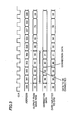
- the CPU 13 outputs the address in synchronization with a clock CLK, and the mask ROM 14 outputs the program data corresponding to the address as shown in Fig. 3 .
- the correction addresses are addresses 301, 302, 303 and 304.
- the outputs from the mask ROM 14 corresponding to the correction addresses 301, 302, 303 and 304 are 75, 80, 92 and 20, respectively, which are the data before the update (bug data) and are to be corrected.
- the ROM correction circuit replaces the grogram data to be corrected that are 75, 80, 92 and 20 with the correction data that are 95, 22, 80 and 21, respectively.
- the correction data 95, 22, 80 and 21 are inputted to the CPU 13 through the selection circuit 17.
- the outputs from the mask ROM 14 at addresses other than the correction addresses, for example at addresses 305 - 309, are 00, 84, 75 and 02. There is no correction data for them because they are correct program data. Therefore, the outputs 00, 84, 75 and 02 from the mask ROM 14 are inputted to the CPU 13 through the selection circuit 17 without changing.
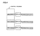
- the ROM correction circuit replaces the bug data with the correction data as described above. Such replacement may be carried out in several locations. As shown in Fig. 4 , each of bug data 1 - 3 in three locations is replaced with each of three correction data 1 - 3, respectively.
- this invention is not limited the above, and may be applied to other audio devices and video devices having a compression decoder to decode compressed data (not only the audio file formats but also video formats) using a control program.
Landscapes
- Engineering & Computer Science (AREA)
- Software Systems (AREA)
- General Engineering & Computer Science (AREA)
- Theoretical Computer Science (AREA)
- Computer Security & Cryptography (AREA)
- Physics & Mathematics (AREA)
- General Physics & Mathematics (AREA)
- Stored Programmes (AREA)
Applications Claiming Priority (1)
| Application Number | Priority Date | Filing Date | Title |
|---|---|---|---|
| JP2009108895A JP2010257367A (ja) | 2009-04-28 | 2009-04-28 | プログラムの更新システム、プログラム更新機能付き電子機器 |
Publications (1)
| Publication Number | Publication Date |
|---|---|
| EP2246784A1 true EP2246784A1 (de) | 2010-11-03 |
Family
ID=42226495
Family Applications (1)
| Application Number | Title | Priority Date | Filing Date |
|---|---|---|---|
| EP10004437A Withdrawn EP2246784A1 (de) | 2009-04-28 | 2010-04-27 | Programmaktualisierungssystem und elektronisches Gerät mit Programmaktualisierungsfunktion |
Country Status (4)
| Country | Link |
|---|---|
| US (1) | US8694717B2 (de) |
| EP (1) | EP2246784A1 (de) |
| JP (1) | JP2010257367A (de) |
| CN (1) | CN101876915B (de) |
Families Citing this family (10)
| Publication number | Priority date | Publication date | Assignee | Title |
|---|---|---|---|---|
| CN104424050B (zh) * | 2013-09-03 | 2019-01-29 | 比亚迪股份有限公司 | 恢复汽车电子设备应用程序的方法、系统及汽车电子系统 |
| CN107357596B (zh) * | 2016-05-09 | 2024-02-13 | 西安中车永电捷通电气有限公司 | 芯片程序更新系统 |
| US10403544B2 (en) | 2016-06-22 | 2019-09-03 | Semiconductor Components Industries, Llc | Semiconductor die singulation methods |
| US9991164B2 (en) | 2016-06-22 | 2018-06-05 | Semiconductor Components Industries, Llc | Semiconductor die singulation methods |
| US11075118B2 (en) | 2016-06-22 | 2021-07-27 | Semiconductor Components Industries, Llc | Semiconductor die singulation methods |
| US10282189B2 (en) * | 2016-06-30 | 2019-05-07 | Synaptics Incorporated | Updating program code stored in an external non-volatile memory |
| CN107943710B (zh) * | 2016-10-13 | 2021-08-27 | 深圳大心电子科技有限公司 | 存储器管理方法及使用所述方法的存储控制器 |
| GB2575482B (en) * | 2018-07-12 | 2023-04-12 | Johnson Electric Int Ag | Actuator system with reprogrammable memory |
| JP7281275B2 (ja) * | 2018-12-20 | 2023-05-25 | Nttエレクトロニクス株式会社 | モジュール及びこれを備える情報処理装置、並びにモジュールのプログラムデータを更新するプログラムデータ更新方法 |
| CN117621665B (zh) * | 2023-12-01 | 2024-07-19 | 珠海趣印科技有限公司 | 一种单mcu通讯的芯片校验方法、耗材芯片和可读存储介质 |
Citations (11)
| Publication number | Priority date | Publication date | Assignee | Title |
|---|---|---|---|---|
| US4542453A (en) * | 1982-02-19 | 1985-09-17 | Texas Instruments Incorporated | Program patching in microcomputer |
| US4751703A (en) * | 1986-09-16 | 1988-06-14 | International Business Machines Corp. | Method for storing the control code of a processor allowing effective code modification and addressing circuit therefor |
| JPH09265391A (ja) | 1996-03-27 | 1997-10-07 | Victor Co Of Japan Ltd | プログラムrom訂正機能付き制御装置及び同制御装置を有する電子機器並びにプログラムの訂正方法 |
| US5974461A (en) * | 1996-06-03 | 1999-10-26 | Webtv Networks, Inc. | Method for automatically regenerating information at a client system in the event of power or communication disruption between the client system and the server |
| JP2002157136A (ja) | 2000-11-16 | 2002-05-31 | Sharp Corp | プログラム機能付き電子機器、そのプログラムデータ訂正装置、及びプログラムデータ訂正システム |
| US6457175B1 (en) * | 1998-11-09 | 2002-09-24 | Tut Systems, Inc. | Method and apparatus for installing a software upgrade within a memory resource associated with a computer system |
| US20030188303A1 (en) * | 2001-03-30 | 2003-10-02 | Barman Roderick A. | Method and apparatus for reprogramming engine controllers |
| JP2004151831A (ja) | 2002-10-29 | 2004-05-27 | Kenwood Corp | プログラム書換システム及びプログラム書換方法 |
| JP2006243997A (ja) | 2005-03-02 | 2006-09-14 | Canon Inc | ダウンロードシステム |
| US20070106430A1 (en) * | 2005-11-04 | 2007-05-10 | Denso Corporation | Vehicle control system having a computer integrated with a rewritable and nonvolatile memory |
| US20080263540A1 (en) * | 2007-04-23 | 2008-10-23 | Konica Minolta Business Technologies, Inc. | Image forming apparatus, program updating system, and program updating program |
Family Cites Families (10)
| Publication number | Priority date | Publication date | Assignee | Title |
|---|---|---|---|---|
| WO1998024021A1 (en) * | 1996-11-29 | 1998-06-04 | Hitachi, Ltd. | Microcomputer control system |
| JP2995030B2 (ja) * | 1998-03-31 | 1999-12-27 | 三洋電機株式会社 | コンピュータシステム、並びにコンピュータシステムにおけるプログラム及びデータの修正方法 |
| JPH11306010A (ja) | 1998-04-22 | 1999-11-05 | Shinko Electric Co Ltd | コンピュータ |
| JP3314749B2 (ja) * | 1999-02-17 | 2002-08-12 | 株式会社デンソー | 電子制御装置 |
| EP1420560A1 (de) * | 2002-11-13 | 2004-05-19 | Thomson Multimedia Broadband Belgium | Softwareaktualisierung über eine USB Verbindung |
| JP2006106914A (ja) * | 2004-10-01 | 2006-04-20 | Fujitsu Ltd | ファームウェアで動作する処理装置およびファームウェア更新方法 |
| JP2006171961A (ja) * | 2004-12-14 | 2006-06-29 | Matsushita Electric Ind Co Ltd | データ再生装置 |
| JP2006178829A (ja) * | 2004-12-24 | 2006-07-06 | Fujitsu Ltd | マイクロコンピュータ |
| JP2008009945A (ja) | 2006-06-30 | 2008-01-17 | Toshiba Corp | メモリシステム |
| US7991866B2 (en) * | 2006-08-18 | 2011-08-02 | Control4 Corporation | Systems and methods for updating a site |
-
2009
- 2009-04-28 JP JP2009108895A patent/JP2010257367A/ja active Pending
-
2010
- 2010-04-21 US US12/764,609 patent/US8694717B2/en not_active Expired - Fee Related
- 2010-04-27 CN CN2010101688237A patent/CN101876915B/zh not_active Expired - Fee Related
- 2010-04-27 EP EP10004437A patent/EP2246784A1/de not_active Withdrawn
Patent Citations (11)
| Publication number | Priority date | Publication date | Assignee | Title |
|---|---|---|---|---|
| US4542453A (en) * | 1982-02-19 | 1985-09-17 | Texas Instruments Incorporated | Program patching in microcomputer |
| US4751703A (en) * | 1986-09-16 | 1988-06-14 | International Business Machines Corp. | Method for storing the control code of a processor allowing effective code modification and addressing circuit therefor |
| JPH09265391A (ja) | 1996-03-27 | 1997-10-07 | Victor Co Of Japan Ltd | プログラムrom訂正機能付き制御装置及び同制御装置を有する電子機器並びにプログラムの訂正方法 |
| US5974461A (en) * | 1996-06-03 | 1999-10-26 | Webtv Networks, Inc. | Method for automatically regenerating information at a client system in the event of power or communication disruption between the client system and the server |
| US6457175B1 (en) * | 1998-11-09 | 2002-09-24 | Tut Systems, Inc. | Method and apparatus for installing a software upgrade within a memory resource associated with a computer system |
| JP2002157136A (ja) | 2000-11-16 | 2002-05-31 | Sharp Corp | プログラム機能付き電子機器、そのプログラムデータ訂正装置、及びプログラムデータ訂正システム |
| US20030188303A1 (en) * | 2001-03-30 | 2003-10-02 | Barman Roderick A. | Method and apparatus for reprogramming engine controllers |
| JP2004151831A (ja) | 2002-10-29 | 2004-05-27 | Kenwood Corp | プログラム書換システム及びプログラム書換方法 |
| JP2006243997A (ja) | 2005-03-02 | 2006-09-14 | Canon Inc | ダウンロードシステム |
| US20070106430A1 (en) * | 2005-11-04 | 2007-05-10 | Denso Corporation | Vehicle control system having a computer integrated with a rewritable and nonvolatile memory |
| US20080263540A1 (en) * | 2007-04-23 | 2008-10-23 | Konica Minolta Business Technologies, Inc. | Image forming apparatus, program updating system, and program updating program |
Non-Patent Citations (1)
| Title |
|---|
| GEIB H ET AL: "FLEXIBLE METHOD FOR CODE ENHANCEMENT OF MASKED PROCESSOR DEVICES", MOTOROLA TECHNICAL DEVELOPMENTS, MOTOROLA INC. SCHAUMBURG, ILLINOIS, US, vol. 35, 1 June 1998 (1998-06-01), pages 64/65, XP000862619, ISSN: 0887-5286 * |
Also Published As
| Publication number | Publication date |
|---|---|
| US8694717B2 (en) | 2014-04-08 |
| US20100274954A1 (en) | 2010-10-28 |
| CN101876915B (zh) | 2013-07-03 |
| JP2010257367A (ja) | 2010-11-11 |
| CN101876915A (zh) | 2010-11-03 |
Similar Documents
| Publication | Publication Date | Title |
|---|---|---|
| US8694717B2 (en) | Program update system and electronic device with program update function | |
| US8869134B2 (en) | Updating firmware on mobile electronice devices | |
| US20090094414A1 (en) | Firmware Update for Storage Device | |
| JP5292978B2 (ja) | 制御装置、情報処理装置、及びメモリモジュール認識方法 | |
| US20110246760A1 (en) | Electronic device and electronic device system | |
| US20140214434A1 (en) | Method for processing sound data and circuit therefor | |
| US20100153622A1 (en) | Data Access Controller and Data Accessing Method | |
| US20190163649A1 (en) | Technique for rffe and spmi register-0 write datagram functional extension | |
| KR100606052B1 (ko) | 이동통신 단말기의 오류 데이터 복구 시스템 및 방법 | |
| EP2194458A2 (de) | Anfrageverarbeitungsvorrichtung, Anfrageverarbeitungssystem und Zugangstestverfahren | |
| JP2008293076A (ja) | エラー判定プログラム、エラー判定方法、及び、電子機器 | |
| US20150012688A1 (en) | Computer system and operating method thereof | |
| US20110022782A1 (en) | Flash storage with array of attached devices | |
| KR100625811B1 (ko) | 코드 데이터 에러 정정 방법 및 장치 | |
| JP2006331185A (ja) | 制御装置、書換装置、書換方法および書換プログラム | |
| US20080188968A1 (en) | Sound data processing apparatus | |
| CN115185478B (zh) | 音频控制电路、主装置及相关的控制方法 | |
| US20090327550A1 (en) | Embedded system and hardware setting method | |
| US20090300223A1 (en) | Method for communication between an electronic device and a target input/output device in a secure digital input/output card through a secure digital interface, and system for implementing the same | |
| CN116157800B (zh) | 数据校准方法和驱动器 | |
| US20090077364A1 (en) | Data-processing arrangement | |
| KR100743252B1 (ko) | 코드 데이터 에러 정정 방법 및 장치 | |
| KR100743253B1 (ko) | 코드 데이터 에러 정정 방법 및 장치 | |
| EP4068107A1 (de) | Audiosteuerungsschaltung, host-vorrichtung und zugehöriges steuerungsverfahren | |
| CN117666932A (zh) | 支持访问多种存储介质的读写装置 |
Legal Events
| Date | Code | Title | Description |
|---|---|---|---|
| PUAI | Public reference made under article 153(3) epc to a published international application that has entered the european phase |
Free format text: ORIGINAL CODE: 0009012 |
|
| AK | Designated contracting states |
Kind code of ref document: A1 Designated state(s): AT BE BG CH CY CZ DE DK EE ES FI FR GB GR HR HU IE IS IT LI LT LU LV MC MK MT NL NO PL PT RO SE SI SK SM TR |
|
| AX | Request for extension of the european patent |
Extension state: AL BA ME RS |
|
| 17P | Request for examination filed |
Effective date: 20110503 |
|
| STAA | Information on the status of an ep patent application or granted ep patent |
Free format text: STATUS: THE APPLICATION IS DEEMED TO BE WITHDRAWN |
|
| 18D | Application deemed to be withdrawn |
Effective date: 20141101 |