EP2194458A2 - Anfrageverarbeitungsvorrichtung, Anfrageverarbeitungssystem und Zugangstestverfahren - Google Patents
Anfrageverarbeitungsvorrichtung, Anfrageverarbeitungssystem und Zugangstestverfahren Download PDFInfo
- Publication number
- EP2194458A2 EP2194458A2 EP09175626A EP09175626A EP2194458A2 EP 2194458 A2 EP2194458 A2 EP 2194458A2 EP 09175626 A EP09175626 A EP 09175626A EP 09175626 A EP09175626 A EP 09175626A EP 2194458 A2 EP2194458 A2 EP 2194458A2
- Authority
- EP
- European Patent Office
- Prior art keywords
- request
- test
- response
- processor
- write
- Prior art date
- Legal status (The legal status is an assumption and is not a legal conclusion. Google has not performed a legal analysis and makes no representation as to the accuracy of the status listed.)
- Withdrawn
Links
Images




Classifications
-
- G—PHYSICS
- G06—COMPUTING OR CALCULATING; COUNTING
- G06F—ELECTRIC DIGITAL DATA PROCESSING
- G06F11/00—Error detection; Error correction; Monitoring
- G06F11/22—Detection or location of defective computer hardware by testing during standby operation or during idle time, e.g. start-up testing
-
- G—PHYSICS
- G06—COMPUTING OR CALCULATING; COUNTING
- G06F—ELECTRIC DIGITAL DATA PROCESSING
- G06F11/00—Error detection; Error correction; Monitoring
- G06F11/22—Detection or location of defective computer hardware by testing during standby operation or during idle time, e.g. start-up testing
- G06F11/2205—Detection or location of defective computer hardware by testing during standby operation or during idle time, e.g. start-up testing using arrangements specific to the hardware being tested
- G06F11/2221—Detection or location of defective computer hardware by testing during standby operation or during idle time, e.g. start-up testing using arrangements specific to the hardware being tested to test input/output devices or peripheral units
-
- G—PHYSICS
- G06—COMPUTING OR CALCULATING; COUNTING
- G06F—ELECTRIC DIGITAL DATA PROCESSING
- G06F11/00—Error detection; Error correction; Monitoring
- G06F11/22—Detection or location of defective computer hardware by testing during standby operation or during idle time, e.g. start-up testing
- G06F11/26—Functional testing
- G06F11/263—Generation of test inputs, e.g. test vectors, patterns or sequences ; with adaptation of the tested hardware for testability with external testers
Definitions
- Embodiments discussed herein relate to an access test technology in a request processing device and a request processing system for relaying a request and a response for access and controlling access to a storage device in order to read/write data from/into the storage device.
- a computer system When a computer system is designed or set up, verification of various types of operations is performed. For example, in a computer system having a central processing unit (CPU) or a processor, an input/output (I/O) device and a memory, a method in which a test program is executed by the CPU to generate memory access has been utilized for performing verification of a dual inline memory module (DIMM) and a memory access control section.
- DIMM dual inline memory module
- test circuit which performs memory access in order to access a specified address without execution of an instruction using a CPU, thereby verifying an operation.
- a test circuit that performs verification of an operation of an interface that is operating as a single device for verifying an external interface.
- a test circuit is known in which an output terminal of an interface is connected to an input terminal thereof to form a return path for testing a serial interface circuit.
- a test pattern is generated by a test pattern generating unit at the output terminal when the test is performed, and an operation check is performed by a matching circuit for matching of the test pattern at the input terminal.
- test circuits performs verification of a memory or a circuit without setting up a system after all peripheral devices are connected to the system in a practical manner, and without running a test program on the system.
- Embodiments of the present invention are made to solve the above-described issues.
- a request processing device includes a request sender that sends a write request or a read request to a storage device, a response processor that receives a response to a request which the request sender has sent, and a test request processor that converts a read response, which is a response to a read request, into a test write request, and converts a write response which is a response to a write request into a test read request, from among responses that the response processor has received or from among responses that have been input from a device which is provided outside the request processing device.
- FIG. 1 is a diagram illustrating a configuration of a system chip according to an embodiment.
- the system chip is a request processing system including an IO request processing section which is a request processing device.
- FIG. 2 is a diagram illustrating a configuration of a computer system having the system chip.
- a computer system 1 includes a CPU 2, a system chip 3, a DIMM (Direct Inline Memory Module) 4, an IO (Input/Output) control chip 5, and a disk device 6.
- the CPU 2 is an arithmetic processing device that performs arithmetic processes, and uses the DIMM 4 as the main memory.
- the disk device 6 is an auxiliary storage device that is a hard disk drive (HDD) for example.
- the IO control chip 5 performs a process of controlling inputting data to or outputting data from to the disk device 6.
- the system chip 3 exists among the CPU 2, the DIMM 4, and the IO control chip 5.
- the system chip 3 is a circuit that relays a request and a response for access and that controls access to the DIMM 4, which is a memory, or to the disk device 6.
- the system chip 3 has a serial interface 34, an IO request processing section 33, a memory access control section 32, a CPU interface 31, and a management section 35 there inside.
- the serial interface 34 is an interface having a serial connection with the IO control chip 5.
- the IO request processing section 33 is connected to the IO control chip 5 via the serial interface 34, and processes an input/output request from the disk device 6.
- the CPU interface 31 is an interface that is connected to the CPU 2.
- the memory access control section 32 is an interface that is connected to the DIMM 4.
- the memory access control section 32 controls access from the CPU 2 to the DIMM 4 via the CPU interface 31, and access from the disk device 6 to the DIMM 4 via the IO request processing section 33, the serial interface 34, and the IO control chip 5.
- the management section 35 is a processing section that performs setting for an operation of the IO request processing section 33.
- the IO request processing section 33 operates in two operation modes, i.e., a normal mode and a test mode.
- the operation mode of the IO request processing section 33 can be switched by the management section 35.
- the management section 35 specifies the details of an operation of the IO request processing section 33 in the test mode.
- the IO request processing section 33 relays, to the memory access control section 32, a request to the DIMM 4 that is input from the serial interface 34, without processing the request.
- the request to the DIMM 4 includes a store request which is a request to write data into the DIMM 4, and a fetch request which is a request to read data from the DIMM 4.
- the memory access control section 32 processes a store request or a fetch request that has been received from the IO request processing section 33, and returns a process result as a response to the IO request processing section 33.
- the IO request processing section 33 that is operating in the normal mode relays the response that has been input from the memory access control section 32 to the serial interface 34, without processing the response.
- the memory access control section 32 makes a response to a request that the IO request processing section 33 made, and the response is converted into another request.
- the converted request is sent to the memory access control section 32.
- the IO request processing section 33 converts a store response into a fetch request, and sends the fetch request to the memory access control section 32. Furthermore, the IO request processing section 33 converts the fetch response from the memory access control section 32 into a store request, and sends the store request to the memory access control section 32.
- a data portion of the fetch response e.g., the contents of data that is read from an address which is specified in the fetch request
- a data portion of the store request e.g., the contents of data that is to be written into an address which is specified in the store request.
- the memory access control section 32 also processes a store request or a fetch request that is generated by a conversion process performed by the IO request processing section 33 as in the case in which the memory access control section 32 operates in the normal mode.
- the memory access control section 32 then returns a response corresponding to a process result to the IO request processing section 33.
- the IO request processing section 33 converts the received response into another request.
- a request and a response are repeated between the IO request processing section 33 and the memory access control section 32, and memory access continues until the test mode is terminated.
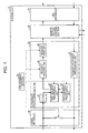
- the IO request processing section 33 has a latch 41, a test request processor 42, a test address processor 43, a request holding unit 44, a request read unit 45 and a request response processor 46 there inside.
- the latch 41 temporarily holds a packet that is inputted from the serial interface 34. While the system chip 3 is operating in the normal mode, a packet that the latch 41 holds, i.e., a packet that is input from the serial interface 34, is provided as a request from the IO control chip 5. While the system chip 3 is operating in the normal mode, the test request processor 42 sends the request that is held in the latch 41 to the request holding unit 44 without processing the request.
- a packet that the latch 41 holds is provided as a response to a request that was sent from the IO request processing section 33 before.
- the test request processor 42 converts the response that is held in the latch 41 into a request if necessary, and sends the request to the request holding unit 44.
- test request processor 42 operates only in the test mode to convert a response packet into a request packet.
- the operation mode of the test request processor 42 is switched between the normal mode or the test mode by the management section 35 as already described.
- the test address processor 43 specifies the details of conversion of an address portion of the packet to be converted.
- the test address processor 43 has three address registers (not illustrated). That is, the three address registers are an OVL_ADRS that holds a test address, an END_ADRS for determining the upper limit of the test address, which is an end address, and a START_ADRS for determining the lower limit of the test address, that is a start address.
- the test address processor 43 increments the test address in the OVL_ADRS.
- the test address processor 43 resets the test address in the OVL_ADRS to be the value of the start address in the START_ADRS.
- the start address, the end address and the test address are set by the management section 35 in the START_ADRS, the END_ADRS, and the OVL_ADRS of the serial interface 34, respectively.
- the serial interface 34 repeatedly specifies an address range that is set using the start address and the end address by the management section 35.
- the request holding unit 44 temporarily holds one request or a plurality of requests that are sent from the test request processor 42.
- the request holding unit 44 always holds a request, because sending of a request from the test request processor 42 is performed even when the system chip 3 is operating in the normal mode or operating in the test mode.
- the request read unit 45 reads a request that the request holding unit 44 holds, and outputs the request to the memory access control section 32.
- the request response processor 46 receives a response to a request from the memory access control section 32.
- the request response processor 46 temporarily stores the response, and outputs the response to the serial interface 34.
- the request response processor 46 performs protocol conversion if protocol conversion is necessary.
- the response that the request response processor 46 has received is supplied to the test request processor 42. Accordingly, in an example illustrated in FIG. 3 , a return path in which a response that the IO request processing section 33 has outputted is returned to the latch 41 of the IO request processing section 33 without being processed is provided in the serial interface 34.
- the serial interface 34 has the two operation modes, i.e., the test mode and the normal mode.
- the serial interface 34 When the serial interface 34 operates in the test mode, the serial interface 34 functions as a return input section that returns a response to the IO request processing section 33.
- a configuration in a case in which a response from the IO request processing section 33 is retuned in the serial interface 34 is described as an example.
- the IO request processing section 33 may have a return path there inside.
- a configuration may be used, in which, outside the system chip 3, an output terminal of the serial interface 34 is connected to an input terminal of the serial interface 34 so that a response can be returned.
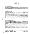
- FIG. 4 illustrates formats of a request packet and a response packet.
- a packet provided as a fetch request has an Opecode field showing a type of packet, in which information indicating that the packet is provided as a fetch request is stored. Further, the packet provided as a fetch request has an ADRS field in which an address from which data is to be read is stored, and an RQID field in which an identifier for identifying and managing the packet is stored.
- a packet provided as a store request has an Opecode field showing a type of packet, in which information indicating that the packet is provided as a store request is stored. Further, the packet provided as a store request has an ADRS field in which an address into which data is to be written is stored, an RQID field in which an identifier for identifying and managing the packet is stored, and a DATA filed in which data to be written is stored.
- a packet provided as a fetch response has an Opecode field showing a type of packet, in which information indicating that the packet is provided as a fetch response is stored. Further, the packet provided as a fetch response has a Status field for recognizing an error response, an address exception, and so forth, an RQID field in which an identifier for identifying and managing the packet is stored, and a DATA field in which data that has been read is stored.
- a packet provided as a store response has an Opecode field showing a type of packet, in which information indicating that the packet is provided as a store response is stored. Further, the packet provided as a fetch response has a Status field for recognizing an error response, an address exception, and so forth, and an RQID field in which an identifier for identifying and managing the packet is stored.
- each of the packet provided as a fetch request and the packet provided as a store response is sent and received in one cycle.
- five cycles are necessary to send and receive the entire packet because four cycles are used to send and receive the DATA field.
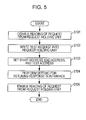
- the management section 35 controls the request read unit 45 to disable reading of a request from the request holding unit 44 (S101). With the control of disabling reading of a request, access to the memory is stopped.
- the management section 35 writes a test request into the request holding unit 44 (S102).
- the written test request indicates details of a first request in the test mode, and may be a fetch request or a store request.
- the management section 35 sets the start address, the end address and the test address in the START_ADRS, the END_ADRS and the OVL_ADRS of the test address processor 43, respectively (S103).
- the management section 35 performs setting for returning a response in the serial interface 34 (S104). Note that, a case in which the serial interface 34 has a return path there inside, and the management section 35 controls the serial interface 34 is supposed herein.
- the management section 35 sets the return path, which is provided inside the IO request processing section 33, to be enabled. Furthermore, in a case in which terminals are to be connected to each other outside the system chip 3, an operator directly will connect the terminals to each other. Note that the order of the processes in S102 to S104 can be appropriately changed.
- the management section 35 controls the request read unit 45 to enable reading of a request from the request holding unit 44 (S105), and terminates the process.
- the request read unit 45 reads a request from the request holding unit 44, and outputting of a request from the IO request processing section 33 starts, and the system chip 3 operates in the test mode.
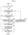
- the test request processor 42 checks whether or not the operation mode is the test mode (S201). When the operation mode is not the test mode (No in S201), the test request processor 42 outputs a packet that is read from the latch 41 to the request holding unit 44, without processing the packet (S208), and terminates the process.
- the test request processor 42 determines whether or not the contents of a packet that is held in the latch 41 are a header portion of a fetch response (S202).
- the test request processor 42 rewrites the Opecode field of the header portion of the fetch response to convert the fetch response into a store request (S204).
- the test request processor 42 determines whether or not the contents of the packet that is held in the latch 41 are a header portion of a store response (S203). As a result, when the contents of the packet that is held in the latch 41 are not a header portion of a store response either (No in S203), the test request processor 42 outputs the packet that is read from the latch 41 to the request holding unit 44, without processing the packet (S208), and terminates the process.
- test request processor 42 rewrites the Opecode field of the header portion of the store response to convert the store response into a fetch request (S205).
- test request processor 42 After the test request processor 42 rewrites the Opecode field of the header portion, the test request processor 42 sets the test address (in the OVL_ADRS), which the test address processor 43 holds, in the ADRS field of the header portion (S206), and instructs the test address processor 43 to update the test address (S207).
- test address processor 43 outputs the request that has been generated by conversion of the response to the request holding unit 44 (S208), and terminates the process.
- test address processor 43 A process of updating the test address, which is performed by the test address processor 43, will be described with reference to FIG. 7 .
- the test address processor 43 terminates the process.
- the test address processor 43 compares the value of the test address in the OVL_ADRS with the value of the end address in the END_ADRS (S302).
- the test address processor 43 sets the value of the start address in the START_ADRS as the test address in the OVL_ADRS (S303), and terminates the process.
- the test address processor 43 adds a predetermined value to the value of the test address in the OVL_ADRS, and terminates the process.
- FIG. 8 is an explanatory diagram for explaining the operation in the normal mode.
- a fetch request (Fch) that the serial interface 34 holds in a first cycle is moved to and held in the latch 41 in a second cycle. Then, in a third cycle, the fetch request is moved to and held in the request holding unit 44. In a fourth cycle, the fetch request is moved to and held in the request read unit 45.
- the fetch request is moved to and processed by the memory access control section 32, and a fetch response is returned.
- the request response processor 46 receives a header portion (Rtn) of the fetch response.
- the request response processor 46 receives a data portion (data) of the fetch response.
- the test address processor 43 receives the header portion of the fetch response.
- the serial interface 34 receives the data portion of the fetch response.
- test address in the OVL_ADRS the end address in the END_ADRS and the start address in the START_ADRS are not used.
- FIG. 9 is an explanatory diagram for explaining the operation in the test mode.
- a state in which a request is held in the request holding unit 44 is an initialization state. Furthermore, in the initialization state, it is supposed that "zero” is set as the test address in the OVL_ADRS, “eight” is set as the end address in the END_ADRS and "zero” is set as the start address in the START_ADRS of the test address processor 43. Note that, in FIG. 9 , in order to distinguish the differences between FIG. 8 and FIG. 9 from each other, the operation starts in a third cycle.
- a fetch request (Fch) that the request holding unit 44 holds in a third cycle is moved to and held in the request read unit 45 in a fourth cycle. Then, in a fifth cycle, the fetch request is moved to and processed by the memory access control section 32, and a fetch response is returned.
- the request response processor 46 receives a header portion (Rtn) of the fetch response.
- the request response processor 46 receives a data portion (data) of the fetch response.
- the test address processor 43 receives the header portion of the fetch response.
- the serial interface 34 receives the data portion of the fetch response.
- the serial interface 34 sends a response to the outside.
- a response is retuned, and transmitted to a sending side.
- a sending side of the serial interface 34 holds the header portion of the fetch response.
- the sending side of the serial interface 34 holds the data portion of the fetch response.
- the latch 41 holds the header portion of the fetch response.
- the latch 41 holds the data portion of the fetch response.
- the test request processor 42 rewrites the header portion of the fetch response, which the latch 41 holds in the (n+3)-th cycle, to convert the fetch response into a store request (STR), and sends the store request to the request holding unit 44.
- an address in which data is to be stored is "zero" that is the value of the test address.
- the test address processor 43 is instructed by the test request processor 42 to update the test address.
- the test address processor 43 updates the value of the test address in the OVL_ADRS to be "one".
- the data portion of the fetch response which is held in the latch 41 in the (n+4)-th cycle to the (n+7)-th cycle, is sent to the request holding unit 44 without being processed.
- the request holding unit 44 holds a header portion of the store request.
- the request holding unit 44 holds a data portion of the store request, and the data portion is treated as data, which is to be written in the store request.
- the request read unit 45 holds the header portion of the store request.
- the request read unit 45 holds the data portion of the store request.
- the memory access control section 32 receives the header portion of the store request.
- the memory access control section 32 receives the data portion of the store request.
- the system chip 3 has the test mode that is an operation mode for testing.
- the system chip 3 returns a response to a request, and converts the response into a new request, thereby reusing a data portion of the response. Accordingly, access test can be easily and efficiently performed on the memory without dependence on a state in which other system elements such as the CPU are mounted.
- the system chip 3 when the system chip 3 according to the present embodiment operates in the test mode, the system chip 3 uses the same circuit used in the normal operation, and processes the same requests that are used in a practical operation. Accordingly, the system chip 3 can perform verification and testing of not only an operation of the memory that is operating as a single device but also of an operation of the entire circuit.
- the state of check functions for data and protocols, which are performed by each of the control sections in the normal operation is held so that the check functions are enabled, whereby the system chip 3 can guarantee, using the check functions, that access for writing and reading data is correctly performed in the test mode.
- the check functions whether or not data that is read from the DIMM 4 is correct can be checked using a check function with error correction code (ECC) that was generated when the data was written into the DIMM 4.
- ECC error correction code
- Whether or not data that is input from the serial interface 34 is correct can be checked using a check function with cyclic redundancy check (CRC) that was performed when the data was output to the serial interface 34.
- ECC error correction code
- the system chip 3 specifies an address range to be accessed, and can semi-permanently continue accessing the range. Accordingly, the system chip 3 can perform a long-duration test of memory access without using the CPU. Note that, when the system chip 3 changes or checks a setting for the start address, the end address, data to be written or read, or the like, it is only necessary that the system chip 3 perform the processes in the flowchart illustrated in FIG. 5 again. When the system chip 3 disables reading of a request from the request holding unit 44 and waits a fixed time, all requests that were being processed have been processed, and access is stopped while a request is being held in the request holding unit 44. Thus, no side effect that is caused by the request holding unit 44 that operates while the setting is being changed occurs.
- a test program is generated at the CPU side under the assumption that access conflict occurs, whereby a long-duration test can be performed in a more complicated state in which conflict between access from the CPU 2 and access from the IO control chip 5 is considered.
Landscapes
- Engineering & Computer Science (AREA)
- General Engineering & Computer Science (AREA)
- Theoretical Computer Science (AREA)
- Computer Hardware Design (AREA)
- Quality & Reliability (AREA)
- Physics & Mathematics (AREA)
- General Physics & Mathematics (AREA)
- Test And Diagnosis Of Digital Computers (AREA)
- Techniques For Improving Reliability Of Storages (AREA)
- For Increasing The Reliability Of Semiconductor Memories (AREA)
Applications Claiming Priority (1)
| Application Number | Priority Date | Filing Date | Title |
|---|---|---|---|
| JP2008311498A JP5309938B2 (ja) | 2008-12-05 | 2008-12-05 | 要求処理装置、要求処理システムおよびアクセス試験方法 |
Publications (2)
| Publication Number | Publication Date |
|---|---|
| EP2194458A2 true EP2194458A2 (de) | 2010-06-09 |
| EP2194458A3 EP2194458A3 (de) | 2014-01-22 |
Family
ID=41582085
Family Applications (1)
| Application Number | Title | Priority Date | Filing Date |
|---|---|---|---|
| EP09175626.2A Withdrawn EP2194458A3 (de) | 2008-12-05 | 2009-11-11 | Anfrageverarbeitungsvorrichtung, Anfrageverarbeitungssystem und Zugangstestverfahren |
Country Status (5)
| Country | Link |
|---|---|
| US (1) | US8291270B2 (de) |
| EP (1) | EP2194458A3 (de) |
| JP (1) | JP5309938B2 (de) |
| KR (1) | KR101106606B1 (de) |
| CN (1) | CN101751311B (de) |
Families Citing this family (4)
| Publication number | Priority date | Publication date | Assignee | Title |
|---|---|---|---|---|
| US20120203765A1 (en) * | 2011-02-04 | 2012-08-09 | Microsoft Corporation | Online catalog with integrated content |
| CN107688515B (zh) * | 2016-12-23 | 2020-11-03 | 北京国睿中数科技股份有限公司 | 一种Bufferable模式的验证方法 |
| TWI732642B (zh) * | 2020-08-03 | 2021-07-01 | 群聯電子股份有限公司 | 資料寫入方法、記憶體控制電路單元以及記憶體儲存裝置 |
| CN115686164A (zh) * | 2021-07-26 | 2023-02-03 | 瑞昱半导体股份有限公司 | 供电端装置、供电系统以及非暂态电脑可读取媒体 |
Citations (3)
| Publication number | Priority date | Publication date | Assignee | Title |
|---|---|---|---|---|
| JPH05342111A (ja) | 1992-06-08 | 1993-12-24 | Nec Corp | メモリ試験方式 |
| JP2001067274A (ja) | 1999-08-27 | 2001-03-16 | Nec Kofu Ltd | 主記憶装置の自己診断方式および方法 |
| JP2005182263A (ja) | 2003-12-17 | 2005-07-07 | Fujitsu Ltd | メモリ試験機能付きコントローラ及びコンピュータ |
Family Cites Families (10)
| Publication number | Priority date | Publication date | Assignee | Title |
|---|---|---|---|---|
| JPH05342113A (ja) * | 1992-06-05 | 1993-12-24 | Japan Aviation Electron Ind Ltd | 組み込み型システムのramの故障検出方法 |
| US5469443A (en) * | 1993-10-01 | 1995-11-21 | Hal Computer Systems, Inc. | Method and apparatus for testing random access memory |
| US5640509A (en) * | 1995-10-03 | 1997-06-17 | Intel Corporation | Programmable built-in self-test function for an integrated circuit |
| SG63746A1 (en) * | 1996-09-20 | 1999-03-30 | Texas Instruments Inc | Method and system for testing memory |
| JP3298621B2 (ja) * | 1998-09-02 | 2002-07-02 | 日本電気株式会社 | 組込み自己テスト回路 |
| JP3871471B2 (ja) * | 1999-07-12 | 2007-01-24 | 松下電器産業株式会社 | Ecc回路搭載半導体記憶装置及びその検査方法 |
| US7200787B2 (en) * | 2003-06-03 | 2007-04-03 | Intel Corporation | Memory channel utilizing permuting status patterns |
| KR100639992B1 (ko) * | 2004-12-14 | 2006-10-31 | 한국전자통신연구원 | 클라이언트 모듈을 안전하게 배포하는 보안 장치 및 그방법 |
| KR100663362B1 (ko) * | 2005-05-24 | 2007-01-02 | 삼성전자주식회사 | 반도체 메모리 장치 및 이 장치의 데이터 라이트 및 리드방법 |
| JP4617282B2 (ja) * | 2006-08-31 | 2011-01-19 | 富士通株式会社 | 負荷発生装置及び負荷試験方法 |
-
2008
- 2008-12-05 JP JP2008311498A patent/JP5309938B2/ja not_active Expired - Fee Related
-
2009
- 2009-10-29 US US12/608,293 patent/US8291270B2/en not_active Expired - Fee Related
- 2009-11-11 EP EP09175626.2A patent/EP2194458A3/de not_active Withdrawn
- 2009-11-18 KR KR1020090111250A patent/KR101106606B1/ko not_active Expired - Fee Related
- 2009-11-26 CN CN2009102263890A patent/CN101751311B/zh not_active Expired - Fee Related
Patent Citations (3)
| Publication number | Priority date | Publication date | Assignee | Title |
|---|---|---|---|---|
| JPH05342111A (ja) | 1992-06-08 | 1993-12-24 | Nec Corp | メモリ試験方式 |
| JP2001067274A (ja) | 1999-08-27 | 2001-03-16 | Nec Kofu Ltd | 主記憶装置の自己診断方式および方法 |
| JP2005182263A (ja) | 2003-12-17 | 2005-07-07 | Fujitsu Ltd | メモリ試験機能付きコントローラ及びコンピュータ |
Also Published As
| Publication number | Publication date |
|---|---|
| CN101751311B (zh) | 2012-10-03 |
| JP5309938B2 (ja) | 2013-10-09 |
| EP2194458A3 (de) | 2014-01-22 |
| JP2010134789A (ja) | 2010-06-17 |
| KR20100065096A (ko) | 2010-06-15 |
| KR101106606B1 (ko) | 2012-01-20 |
| CN101751311A (zh) | 2010-06-23 |
| US8291270B2 (en) | 2012-10-16 |
| US20100146224A1 (en) | 2010-06-10 |
Similar Documents
| Publication | Publication Date | Title |
|---|---|---|
| JP4550439B2 (ja) | Ecc制御装置 | |
| JP4600518B2 (ja) | 情報処理装置、情報処理システム、および情報処理方法、並びにコンピュータ・プログラム | |
| US20040255225A1 (en) | Control circuit for error checking and correction and memory controller | |
| JP5292978B2 (ja) | 制御装置、情報処理装置、及びメモリモジュール認識方法 | |
| JP2010140127A (ja) | データ転送処理装置及び方法 | |
| US20230236742A1 (en) | NONVOLATILE MEMORY EXPRESS (NVMe) OVER COMPUTE EXPRESS LINK (CXL) | |
| CN108459876B (zh) | 用于缩减面积的控制寄存器电路的方法与装置 | |
| KR20210108466A (ko) | 시퀀스 프로세싱 유닛이 있는 메모리 제어 시스템 | |
| KR100988157B1 (ko) | 메모리 디바이스 구성을 검출하기 위한 방법 및 장치와, 메모리 디바이스 구성을 검출하기 위한 방법을 수행하기 위한 명령들을 포함하는 컴퓨터 판독 가능 매체 | |
| EP2194458A2 (de) | Anfrageverarbeitungsvorrichtung, Anfrageverarbeitungssystem und Zugangstestverfahren | |
| JP2008139908A (ja) | メモリ制御装置、コンピュータシステム及びデータ再生記録装置 | |
| US20100153622A1 (en) | Data Access Controller and Data Accessing Method | |
| US20240184484A1 (en) | Flash memory controller and associated memory device and control method | |
| JP5917325B2 (ja) | ブリッジ回路 | |
| JP4793798B2 (ja) | マイクロコンピュータ | |
| US12493508B2 (en) | Information processing apparatus and method | |
| US12393368B2 (en) | Flash memory controller and associated memory device and control method | |
| JP2012048277A (ja) | 半導体集積回路、デバッグシステム、デバッグ方法、デバッグプログラム及び記録媒体 | |
| US8533565B2 (en) | Cache controller and cache controlling method | |
| JP2010079372A (ja) | 記憶装置、バステスト方法、及びデータ転送モード切替方法 | |
| JP2004126911A (ja) | 制御装置 | |
| WO2024190403A1 (ja) | 半導体装置、およびそれを備えた情報処理装置 | |
| JP5439742B2 (ja) | システムコントローラ、半導体装置、及びインターフェイス試験方法 | |
| CN117220861A (zh) | 秘钥烧录系统、方法、智能网卡以及可读存储介质 | |
| CN118394281A (zh) | 数据读取方法、装置和芯片 |
Legal Events
| Date | Code | Title | Description |
|---|---|---|---|
| PUAI | Public reference made under article 153(3) epc to a published international application that has entered the european phase |
Free format text: ORIGINAL CODE: 0009012 |
|
| AK | Designated contracting states |
Kind code of ref document: A2 Designated state(s): AT BE BG CH CY CZ DE DK EE ES FI FR GB GR HR HU IE IS IT LI LT LU LV MC MK MT NL NO PL PT RO SE SI SK SM TR |
|
| AX | Request for extension of the european patent |
Extension state: AL BA RS |
|
| PUAL | Search report despatched |
Free format text: ORIGINAL CODE: 0009013 |
|
| AK | Designated contracting states |
Kind code of ref document: A3 Designated state(s): AT BE BG CH CY CZ DE DK EE ES FI FR GB GR HR HU IE IS IT LI LT LU LV MC MK MT NL NO PL PT RO SE SI SK SM TR |
|
| AX | Request for extension of the european patent |
Extension state: AL BA RS |
|
| RIC1 | Information provided on ipc code assigned before grant |
Ipc: G06F 11/267 20060101AFI20131218BHEP Ipc: G06F 11/22 20060101ALI20131218BHEP |
|
| 17P | Request for examination filed |
Effective date: 20140326 |
|
| RBV | Designated contracting states (corrected) |
Designated state(s): AT BE BG CH CY CZ DE DK EE ES FI FR GB GR HR HU IE IS IT LI LT LU LV MC MK MT NL NO PL PT RO SE SI SK SM TR |
|
| 17Q | First examination report despatched |
Effective date: 20151207 |
|
| GRAP | Despatch of communication of intention to grant a patent |
Free format text: ORIGINAL CODE: EPIDOSNIGR1 |
|
| INTG | Intention to grant announced |
Effective date: 20170518 |
|
| STAA | Information on the status of an ep patent application or granted ep patent |
Free format text: STATUS: THE APPLICATION IS DEEMED TO BE WITHDRAWN |
|
| 18D | Application deemed to be withdrawn |
Effective date: 20170929 |