EP2245729B1 - Schaltung und leistungsgleichrichterysteme, entsprechendes verfahren, solche schaltung oder systeme enthaltendes fluggerät - Google Patents
Schaltung und leistungsgleichrichterysteme, entsprechendes verfahren, solche schaltung oder systeme enthaltendes fluggerät Download PDFInfo
- Publication number
- EP2245729B1 EP2245729B1 EP09716653.2A EP09716653A EP2245729B1 EP 2245729 B1 EP2245729 B1 EP 2245729B1 EP 09716653 A EP09716653 A EP 09716653A EP 2245729 B1 EP2245729 B1 EP 2245729B1
- Authority
- EP
- European Patent Office
- Prior art keywords
- boost
- circuit
- cell
- cells
- terminal
- Prior art date
- Legal status (The legal status is an assumption and is not a legal conclusion. Google has not performed a legal analysis and makes no representation as to the accuracy of the status listed.)
- Active
Links
Images


Classifications
-
- H—ELECTRICITY
- H02—GENERATION; CONVERSION OR DISTRIBUTION OF ELECTRIC POWER
- H02M—APPARATUS FOR CONVERSION BETWEEN AC AND AC, BETWEEN AC AND DC, OR BETWEEN DC AND DC, AND FOR USE WITH MAINS OR SIMILAR POWER SUPPLY SYSTEMS; CONVERSION OF DC OR AC INPUT POWER INTO SURGE OUTPUT POWER; CONTROL OR REGULATION THEREOF
- H02M7/00—Conversion of AC power input into DC power output; Conversion of DC power input into AC power output
- H02M7/02—Conversion of AC power input into DC power output without possibility of reversal
- H02M7/04—Conversion of AC power input into DC power output without possibility of reversal by static converters
- H02M7/12—Conversion of AC power input into DC power output without possibility of reversal by static converters using discharge tubes with control electrode or semiconductor devices with control electrode
- H02M7/21—Conversion of AC power input into DC power output without possibility of reversal by static converters using discharge tubes with control electrode or semiconductor devices with control electrode using devices of a triode or transistor type requiring continuous application of a control signal
- H02M7/217—Conversion of AC power input into DC power output without possibility of reversal by static converters using discharge tubes with control electrode or semiconductor devices with control electrode using devices of a triode or transistor type requiring continuous application of a control signal using semiconductor devices only
- H02M7/25—Conversion of AC power input into DC power output without possibility of reversal by static converters using discharge tubes with control electrode or semiconductor devices with control electrode using devices of a triode or transistor type requiring continuous application of a control signal using semiconductor devices only arranged for operation in series, e.g. for multiplication of voltage
-
- H—ELECTRICITY
- H02—GENERATION; CONVERSION OR DISTRIBUTION OF ELECTRIC POWER
- H02M—APPARATUS FOR CONVERSION BETWEEN AC AND AC, BETWEEN AC AND DC, OR BETWEEN DC AND DC, AND FOR USE WITH MAINS OR SIMILAR POWER SUPPLY SYSTEMS; CONVERSION OF DC OR AC INPUT POWER INTO SURGE OUTPUT POWER; CONTROL OR REGULATION THEREOF
- H02M7/00—Conversion of AC power input into DC power output; Conversion of DC power input into AC power output
- H02M7/02—Conversion of AC power input into DC power output without possibility of reversal
- H02M7/04—Conversion of AC power input into DC power output without possibility of reversal by static converters
- H02M7/06—Conversion of AC power input into DC power output without possibility of reversal by static converters using discharge tubes without control electrode or semiconductor devices without control electrode
- H02M7/10—Conversion of AC power input into DC power output without possibility of reversal by static converters using discharge tubes without control electrode or semiconductor devices without control electrode arranged for operation in series, e.g. for multiplication of voltage
Definitions
- the present invention relates to a device and a power rectifying method, an associated system and an aircraft comprising such a device and / or system.
- AC / DC rectifier type functionality where the AC side performs sinusoidal current sampling. in phase with the supply network voltages, in order to optimize the power factor as close as 1, and to obtain optimum energy efficiency and / or to meet quality standards of the distribution network.
- the DC side is the output of such circuits.
- the AC side power supply of such an alternative network may, for example, be an electrical generation system embedded in an aircraft for powering an on-board network and as described in the applications FR-2,881,896 and FR-2,897,731 .
- the DC stage can itself power a DC / DC or DC / AC converter, for example a motor-inverter or a backup power supply.
- circuits have the advantage of being versatile and modular but nevertheless remain rapidly complex because of the large number of transistors and electronic controls applied to the transistors.
- these systems appear less reliable than a passive diode rectifier and have significantly higher power losses due to the presence of twice as many components that generate on average additional losses due to high-frequency switching, and voltage calibration of important components, typically 1200 V in the industry.
- the switching cells are composed of two transistors in series.
- the low impedance failure (or short-circuit) of one of them results in the short-circuiting of the DC bus in which high energy can be stored, including several hundred joules. This energy may be sufficient to cause the explosion of the housings if rapid protection is not activated on the transistors.
- the resulting circuits then quickly have more complex, more expensive and probably with a risk of defeasability compared to a simple passive diode rectifier.
- a network embedded in an aircraft generally has these characteristics, where an alternating generator supplies electrical energy to the entire aircraft.
- the switching cells can no longer be reversible in current and then have only one transistor and one diode, therefore a reduced number of transistors and control means of the transistors. This results in lower cost, reduced risk of circuit control failure and lower power losses.
- Such circuits are thus suitable for applications / equipment requiring powers over a wide range and industrial voltages, for example from 300 V to 1200 V, typically 800 V.
- PFC circuit Power Factor Correction
- rectifier-boost boost
- the boost-rectifiers use as a basis a bridge with six diodes or three branches of rectifiers with 2 or 4 diodes (for all three phases of the power supply) associated with a single or double boost circuit.
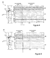
- figure 1 there is shown a double-boost circuit with 2-diode rectifier and has three voltage levels on the AC side which divides by 2 volts-seconds sizing the inductors.
- Each boost cell consists of a diode 100 or 110, a switch 102 or 112 and a capacitor 104 or 114 (defining a DC voltage bus DC).
- boost component for example a boost diode .
- This circuit operates at a switching frequency Fdec corresponding to the repetition frequency of the control commands on the transistors-switches.
- a voltage resistance of all the components ( boost diodes and transistors) reduced by half is also obtained, and a calibration with a margin of tolerance of these components reduces by as much, going from 1200V to 600V.
- the circuit of the figure 1 is already a first step towards greater safety. Indeed, any fault on one of the two transistors is spontaneously isolated by the boost diodes . Short-circuiting of the DC bus is thus avoided in such a scenario.
- This circuit comprises four boost cells 20 to 23.
- the first stage formed of cells 20 and 21 takes up the topology of the circuit of the figure 1 (in the absence of rectifying diodes 13 and 14).
- An identical second stage (cells 22 and 23) has been added after the first stage, thus creating generally AC side five output voltage levels: -E / 2; -E / 4; 0; E / 4; E / 2.
- the presence of the second stage makes it possible to double the switching frequency to 2.Fdec. Frequencies up to a few hundred kilohertz are thus possible allowing an increase in the useful bandwidth if the AC network is of high frequency and a decrease in volts-seconds applied to the inductors implies a decrease in the dimensions of the passive components, in particular the input inductor. This last reduction makes it possible in particular to apply reduced voltages to the components for the same supply voltage and therefore to undersize the components (economic gains), or, at the same rating, to accept much higher supply voltages.
- the increased switching frequency also reduces the value of the capacitances in the boost cells , with the result that a smaller amount of energy is stored in the circuit.
- a boost diode breaks and the transistor of the cell causes the capacity to be short-circuited, the risk of explosion is quickly eliminated.
- This solution also has the advantage of being fault tolerant. Indeed, in the event of a fault of a switch transistor, for example that of the cell 20, the other stage, here the cell 22, continues to cut this time at the switching frequency Fdec (because it maintains the cutting on the active alternation of the supply current despite the faulty cell). In case of failure of a switch, one loses thus, at the price of a static overvoltage (that is to say at the terminals of the diodes) of 50% and dynamic (that is to say at the terminals of the switches / transistors) of 100%, a voltage level output and switching to a simple switching frequency for the upper or lower part affected by this failure.
- a static overvoltage that is to say at the terminals of the diodes
- dynamic that is to say at the terminals of the switches / transistors
- the diodes in the boost cells 20 to 23 must be dimensioned for the totality of the differential voltages of the cell, and therefore of the voltage rating equal to E / 2 (E / 4 + E / 4 for the first stage and E / 2 + E / 2-E / 4-E / 4 for the second stage).
- E 800 V applied in industry
- the switching cells comprise a diode and two pairs of transistor / diode, one of which is static. This implies higher parasitic inductances than in previous circuits.
- the invention aims in particular to solve the aforementioned drawbacks by providing a fault-tolerant multi-level voltage rectifier circuit comprising boost cells , in particular to a single transistor and a single diode per cell.
- a boost cell ensures the cutting despite the failure inside another boost cell, which guarantees a fault tolerance of switches or diodes.
- the circuit according to the invention makes it possible to operate the diodes under a voltage of E / 4 (that is to say 200 V for a voltage source of 800 V) and thus to require, in case of failure , a calibration of E / 2 (that is 400 V), the output voltage.
- E / 4 that is to say 200 V for a voltage source of 800 V
- a calibration of E / 2 that is 400 V
- 600 V calibration components are possible with a reasonable operating margin.
- the invention aims in particular a power rectifier circuit as defined in claim 1.
- the terminal in common is the second output for each of the switching assemblies.
- “Separate” is understood to mean that, for each of the switching assemblies, the corresponding boost cells (i.e., the same stage in the sense of the Figures 2a and 2b ) of the upper part (first switching assembly) and the lower part (second set) do not share components. This results in the absence of stress transfer (" stress" according to the English terminology) in tension for the components between the sets, and therefore a better containment.
- the invention makes it possible to use switch transistors and diodes in the boost cells under voltage E / 4, ie 200 V in the example above, for a 2x2-cell scheme, unlike circuits of FIG. the state of the art.
- the diodes of the boost cells are at most subject to voltages of E / 2, the output voltage.
- the switching frequency and the number of voltages on the AC side are multiplied, in particular according to the number of nested cells, that is to say the number of stages or groups. It is thus possible to effectively reduce the volt-seconds applied to the input inductance (and thus its size) and the switched VA volt-amps, compared to the state of the art, where the switched silicon VAs are defined as the sum of the products between the terminal voltage and the current flowing in each of the circuit transistors of the circuit cells.
- the invention in its configuration with 2 x 2 cells makes it possible to divide in a ratio of 2 to 8 the value of the input inductance, in a ratio 2 the switched silicon volt-amps and finally to reduce the 30% of the losses compared to the solutions of the prior art with the same number of transistors, that is to say the same level of complexity.
- each switching unit may comprise two boost cells .
- This configuration offers a good compromise between a low input inductance and a reasonable number of transistors, thus limiting the stored global energy (compared to the presence of N boost cells , ie 2N capacitances if N "2).
- a switch assembly it is possible for a switch assembly to include more than two boost cells . It is specified here that too many transistors would increase the amount of energy stored on average in the circuit. This provides a maximum of five boost cells per switching set, typically from 2 to 3.
- redundancy cells In order to reinforce the fault circuit, the use of cells or redundancy assemblies can be provided.
- this redundant boost cell being passive, ie in a standby state (transistor-switch permanently on in the on state), during the operation of the other cells.
- the faulty cell Upon detection of a failure of a cell, the faulty cell is replaced by this redundant cell.
- this redundant cell Depending on the position of the switch assembly, it will be necessary to synchronize the switch control signals with the position of each of the operating cells within the switch assembly.
- the redundancy may also relate to a switching assembly that replaces one of the two initial switching assemblies in case of failure of too many boost cells so that the cutting can not be continued. It will be possible to switch from a switching assembly to the redundant assembly by using, for example, a switch.
- the circuit comprises rectifying means.
- the rectifying means comprise a pair of rectifying means arranged to be connected between said supply terminal and respectively each of said switching assemblies so as to rectify the low frequency input current.
- the rectifying means comprise rectifying diodes provided in each boost cell, these rectifying diodes being in series with said switch means and passers in the opposite direction to that of the corresponding boost diode (that is to say of the same cell).
- the boost cells are unidirectional in current (the switching assemblies are also unidirectional by putting the boost cells in series in the same direction), this configuration makes it possible to protect each of the switching assemblies. reverse currents supplied for half a period of the AC power supply (half period during which the other switching assembly is biased).
- the system is arranged to force the switching means (transistors) of one switching unit while the other set is active.
- each rectifying means comprises a diode, in particular placed in series in the same direction as the diodes of the switching assembly to which it is connected.
- each rectifying means comprises a thyristor, in particular placed in series in the same direction as the diodes of the switching assembly to which it is connected.
- the thyristor has the advantage of providing a current control during the precharging phase of the boost capabilities (at E / 2 or E / 4 in the configuration 2x2 cells), especially at the start of the system comprising the circuit.
- these rectifying means are placed in series in the same direction as the diodes of the switching assembly to which they are respectively connected.
- the switch means comprise controlled transistors.
- the circuit comprises blocking means able to block, in case of detection of a low impedance defect in one of the boost cells , all of the switch means of said device.
- the detection can be performed on the floating capacitors (at the output of each boost cell ) or on the switch means.
- the detection of these defects relates to a general problem that can be dissociated from the elements of the invention described above. For this purpose and for the reasons explained later in the description, it may be envisaged to separately protect the solution for detecting a fault in a switching cell in which two controlled switches are not available.
- the circuit may include means for detecting a low-impedance fault in a boost cell arranged to detect the voltage across the switch means of the cell for a duration prefixed consecutively to a triggering command of the switch means for detecting a fault of the boost diode of the cell or consecutively to a blocking control of the switch means for detecting a fault of said switch means.
- said means for detecting a low impedance fault comprise a transistor control coupled to a voltage detector.
- the circuit comprises a power supply terminal arranged to be connected to the power source.
- the invention also relates to an electric power rectifier system provided by a polyphase AC power source, comprising a plurality of power rectifier circuits as presented above and arranged to be each connected to a power supply terminal connected to respectively each phase of the polyphase current, and wherein the circuits share the same terminal capacitors.
- a system capable of straightening a polyphase current, generally bi or tri-phased.
- the invention also relates to an electric power rectifier system provided by an AC power source, comprising two corresponding power rectifier circuits as presented above and arranged to be respectively connected to each of the terminals of the power supply. , and wherein the circuits share the same terminal capabilities.
- a system based on the differential voltage at the terminals of the power source is thus realized.
- a cell of one of the rectifier circuits and the corresponding cell of the other circuit i.e. having the same relative position in each of the rectifier circuits
- share the same capacitance i.e. having the same relative position in each of the rectifier circuits
- the differential voltage configuration requires six rectifying circuits as presented above (2 circuits for the differential voltage for each of the 3 phases) sharing all the same two terminal capacitors.
- the invention also relates to a method of power rectification of an electric current signal supplied by an alternative power source, as defined by claim 8.
- the method comprises a step of detecting a low impedance (or short-circuit) fault in at least one one of said boost cells , and following said detection, a step of blocking said boost cell switch means .
- the blocking consists in passing the switch means in a blocking / closed position, as opposed to the open / open position of the switches. It is thus possible to apply a blocking policy based on a certain number of failures affecting the boost cells , as defined below.
- the switching means of a switching assembly is forced in the on state when the other switching assembly is active on an alternation of the input current. This avoids the application of reverse voltages across the transistors.
- the method may comprise steps and implement means relating to the circuit and system characteristics set forth above.
- the invention also relates to an aircraft comprising a device or a system according to any one of the configurations presented above.
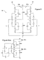
- an exemplary embodiment of the rectifier circuit 30 according to the invention and as illustrated by the figures 3 is based on the switching circuit "double-boost 3 levels AC / DC" presented in
- the circuit of figures 3 applies to a non-differential input voltage.
- the circuit 30 has two separate switching assemblies 30a and 30b each connected to the power supply terminal 31 by a rectifying means, here a rectifying diode 32a and 32b.
- Each of the assemblies 30a and 30b is unidirectional in that they let the current flow in one direction only.
- the two sets also have an opposite direction of passage of the current.
- the rectifying diodes 32a and 32b pass in the same direction as the switching assemblies 30a and 30b to which they are respectively connected.
- the diodes 312i / 322i of the same set 30i are arranged in the same direction.
- Each cell of a stage j is connected to a cell of a stage j + 1 by connecting the diode and the switch of the cell j + 1 to the respective terminals of the capacitor j.
- boost cell of one stage has no part or component in common with the boost cell of the same stage in the other switching unit. This independence ensures that no stress in tension related to the dysfunction of one of the cells affects the cell of the same floor in the other set.
- the diode 312i and the switch 314i of the cell of the first stage 1 are connected to the rectifying diode 32i.
- Each capacitor 326i of the cell of the last stage, here stage 2 is connected to the neutral terminal of the source AC 12 (for a non-differential circuit as is the case on the figures 3 ) by its common terminal with the switch 324i of the same cell.
- these so-called terminal 326i capabilities have one terminal in common and are connected in series.
- Each switching assembly 30i is connected at the output to an output terminal 33i by the terminal of the terminal capacitor 326i common with the diode 322i.
- an equipment (not shown) is connected to be fed to the output terminals 33i.
- the controlled switches 314i and 324i are controlled by one or more control devices known to those skilled in the art (not shown, for example a device per stage j). For the circuit with 2x2 cells boost, one can use control signals similar to those exposed in the aforementioned application FR-2 809 548 for a power supply 12 of the same frequency. Thus, the charging and discharging mechanisms of the four capacitors 316i and 326i are not described in more detail by switching the four switches 314i and 324i.
- the circuit thus makes it possible to obtain AC side voltages (-E / 2, -E / 4, E / 4, E / 2) as well as the potential 0 at the common terminal of the terminal capacitors 326i.
- the AC side voltage then has 2N + 1 voltage levels: -E / 2N, ..., -E / 4, -E / 2, 0, E / 2, E / 4, ..., E / 2N.
- FIG. 40 shows the currents of the three phases of the three-phase source 12 (it is of interest here only to one of this phase, that received by the circuit in question) through the corresponding input inductors 15,
- the transistor 314a goes into low impedance defect, that is to say it becomes permanently on. On the figure 4 This error occurs at time T.
- the diode 312a which is immediately in series then has a voltage at its terminals equal to -E / 4. The diode 312a then becomes blocking and isolates the DC DC bus fault, only the cell 310a concerned is naturally disabled by progressive discharge of the floating capacitor 316a.
- Capacitor 316a is permanently discharged.
- the voltage at its terminals gradually drops to 0 at the instant T + ⁇ t at each switching period, where ⁇ t is the time required for the alternation concerned by the failing transistor to pass in order to allow its discharge. In practice, this value depends mainly on the characteristics of the capacitor 316a.
- the energy released by this uncontrolled discharge is returned to the network (the source 12).
- the diode 312a remains in the blocking state, isolating the failing boost cell 310a.
- the switching assembly 30b is not affected by this failure and continues to operate at 2.Fdec for each of the two cells 310b and 320b.
- the circuit 30 only works with 4 voltage levels: -E / 2, -E / 4, 0 and E / 2.
- the capacitor 316a of the defective cell discharges returning to the network the energy of the defective cell.
- the two switch assemblies 30b are separate, it is also possible to tolerate failure in one of the two cells 310b and 320b. In general, it is possible that the boost cells of a switching assembly fail one after the other. The switching assembly nevertheless ensures that the source current is switched on the relevant alternation as long as at least one healthy cell remains.
- the low frequency rectifying diode 32i can be replaced by a thyristor in order to spontaneously isolate the switching assembly at the zero crossing. This avoids any short circuit of the output bus.
- the figure 5 still illustrates the circuit (left side) and also shows a graph 50 of the three phase currents across the corresponding input inductors and a graph 51 of the voltage across the capacitor of the failed cell.
- the circuit 30 undergoes a low-impedance fault in the controlled transistor 314a at time T.
- the defect undergone is first detected.
- a transistor 80 control is shown coupled to a voltage detector 81 used to detect defects in one of the boost cells. The detection is performed on the basis of the behavior of the voltage across the controlled transistor.
- This circuit being known to those skilled in the art, the components are not described in more detail.
- the graph of the figure 8b illustrates the voltage across the transistor 314a measured by the circuit 80-81 (curve 82 whose part in bold illustrates the normal behavior and the finer parts, a faulty behavior allowing the detection of a fault) following a command passage in the on state (83) and a blocking control (84).
- this system makes it possible to detect any fault of a second component of the boost cell into which the controlled transistor is inserted, here 314a: a fault of the diode 312a is detected in the present case.
- the voltage across the transistor 314a is Vce in the blocking state.
- the transistor is turned on.
- the voltage decreases to a almost zero value (bold curve).
- the voltage goes back to the value Vce after a few ⁇ s, typically 5 ⁇ s.
- a delay of ten ⁇ s after the command 83 is thus provided to detect whether the resulting voltage across the transistor 314a has been modified (normal behavior) or not (faulty behavior of the diode).
- this circuit 80 does not allow the detection of a fault of the same transistor 314a, in particular because no need had been felt because these circuits 80 were generally used in these cells comprising two transistors that then performed mutual monitoring of each other.
- an object of the invention provides for the detection of the fault on the transistor 314a following the control of passage in the blocking state 84.
- this transistor 314a does not maintain the voltage Vce at its terminals consecutively to the control 84, but the voltage at the terminals drops to a value that is almost zero ( fine curve).
- the detection time of the phenomenon is about 5 ⁇ s. A detection period of about ten ⁇ s is therefore provided to determine if there has been no change in the voltage across the transistor following the application of the blocking control 84.
- the switch control device Upon detection of the fault, the switch control device blocks all the switches (in operation) of the circuit 30, as illustrated. by the acronyms OFF on the figure 5 . As seen above, the detection can also relate to a failure of a diode.
- the circuit 30 then corresponds to a simple diode rectifier (diode bridge), as illustrated by graph 51.
- This embodiment can be modulated by setting up different policies for blocking the switches still in operation according to the detection or detections made, in particular the blocking of all the switches can be performed only when the number of failed transistors in the same set of 30i switching reaches a threshold value.
- the latter can be predefined theoretically to define a voltage threshold applied to the diodes, taking into account both the calibration of the boost diodes and the number of stages (since the overvoltage undergone by a failure depends on the number of stages and accumulates with the overvoltage experienced by a second failure in the same switching set).
- this embodiment is used with a polyphase feed, for example three-phase (see figure 7 ).
- a polyphase feed for example three-phase (see figure 7 ).
- all the controlled switches of the circuit (of the same phase) affected by the fault are blocked and the output power of the three-phase system is then adjusted by the circuits 30 2 and 30 3 of the (two) other phases, in particular to preserve the regulation of the DC bus.
- the differential power rectifier system 60 then comprises two circuits 30 and 30 ', in particular identical to the circuit of the circuits. figures 3 , whose power supply terminals 31 and 31 'are respectively connected to an input impedance 15 and 15' connected to the two terminals of the AC power source 12.
- the two circuits 30 and 30 have their output capabilities 326a and 326b in common, so as to form a single output bus of the system 60 between the terminals 33a and 33b.
- switching assemblies which have a common output capacitance, said "corresponding" switching assemblies (for example 30a and 30'a), are not used during the alternation of the current of the source 12. It is then expected to pool the components of two corresponding sets, this mutualization may relate to one or more components.
- the figure 6bis presents the case of maximum mutualisation even if intermediate sharing states are foreseen.
- each switching assembly 30-30'a, 30-30'b is connected by the same terminal to the two terminals of the power supply via rectifying diodes positioned in the opposite direction. It is thus observed that the diodes connected to one and the same switching assembly are mutually exclusive (opposite direction) so that the switching assembly is used successively for each of the two alternations of the source current 12 via each of the two rectifying diodes. .
- This configuration thus permanently uses the four transistors ordered, the applied commands being shifted by 90 ° ( ⁇ / 2) between these different transistors.
- the mutualization may be partial, for example a single switching unit is shared with the corresponding set of the other circuit.
- the differential system thus obtained has in particular 9 voltage levels for a control frequency equal to 4.Fdec.
- the power rectifier system for three-phase power supply 70 comprises three circuits 30 1 , 30 2 and 30 3 , each similar to that of figures 3 , Connected to a stage 12 1, 12 2, 12 3 of the power source 12.
- the three circuits have their terminal capacitors 326a and 326b in common so as to form a single output bus of the system 70 between terminals 33a and 33b.
- the control modulation of the controlled switches of the three circuits is similar.
- the switches having an identical position respectively in each of the three circuits 30 1 , 30 2 and 30 3 are controlled by an offset modulation of the same angle as the phases of the power source, here substantially 2 ⁇ / 3.
Landscapes
- Engineering & Computer Science (AREA)
- Power Engineering (AREA)
- Dc-Dc Converters (AREA)
- Rectifiers (AREA)
Claims (9)
- Leistungsgleichrichterschaltung (30) für durch eine Wechselstromversorgungsquelle (12) gelieferten elektrischen Strom, umfassend:- zwei getrennte Schaltanordnungen (30a, 30b), die dazu eingerichtet sind, an einen Stromversorgungsanschluss (31) der Quelle über Gleichrichtermittel (32a, 32b) angeschlossen zu werden,- wobei die Schaltung dadurch gekennzeichnet ist, dass sie umfasst- ein Paar von Gleichrichtermitteln (32a, 32b), die dazu eingerichtet sind, zwischen dem Stromversorgungsanschluss und jeweils einer jeden der Schaltanordnungen angeschlossen zu werden, um den Niederfrequenzstrom an dem Stromversorgungsanschluss (31) gleichzurichten,- wobei jede Schaltanordnung (30a, 30b) eine Vielzahl von kaskadierten Schaltzellen (310a, 310b, 320a, 320b), sogenannten Boost-Zellen umfasst,- wobei jede Boost-Zelle eine Diode (312a, 312b, 322a, 322b), die zwischen einem ersten Eingangsanschluss und einem ersten Ausgangsanschluss der Zelle angeschlossen ist, ein Schaltermittel (314a, 314b, 324a, 324b), das zwischen einem zweiten Eingangsanschluss und einem zweiten Ausgangsanschluss der Zelle angeschlossen ist, sowie eine Kapazität (316a, 316b, 326a, 326b), die zwischen den beiden Ausgangsanschlüssen der Zelle angeschlossen ist, umfasst,- wobei die Boost-Zellen einer Schaltanordnung in Kaskade geschaltet sind, so dass der erste und der zweite Ausgangsanschluss einer Boost-Zelle an den ersten bzw. den zweiten Eingangsanschluss der folgenden Boost-Zelle angeschlossen sind, wobei der erste und der zweite Eingangsanschluss der ersten Boost-Zelle der Schaltanordnung mit den an die Schaltanordnung angeschlossenen Gleichrichtermitteln (32a, 32b) verbunden sind,- wobei die Kapazitäten, sogenannten Abschlusskapazitäten (326a, 326b), der beiden Abschluss-Boost-Zellen (320a, 320b) der Schaltanordnungen einen gemeinsamen Anschluss haben.
- Schaltung nach dem vorstehenden Anspruch, bei der jede Schaltanordnung zwei Boost-Zellen umfasst.
- Schaltung nach einem der vorstehenden Ansprüche, umfassend Blockiermittel, die geeignet sind, bei Erfassen eines Niedrigimpedanzfehlers an einer der Boost-Zellen alle Schaltermittel der Vorrichtung zu blockieren.
- Schaltung nach dem vorstehenden Anspruch, umfassend Mittel zur Erfassung eines Niedrigimpedanzfehlers in einer Boost-Zelle (310a,b, 320a,b), die dazu eingerichtet sind, die Spannung an den Anschlüssen des Schaltermittels (314a,b, 324a,b) der Zelle über eine zuvor festgelegte Dauer im Anschluss an eine Ansteuerung (83) des Schaltermittels zu erfassen, um einen Ausfall der Boost-Diode (312a,b, 322a,b) der Zelle zu erfassen oder im Anschluss an eine Steuerung zum Blockieren (84) des Schaltermittels, um einen Ausfall des Schaltermittels zu erfassen.
- Leistungsgleichrichtersystem (70) für durch eine Mehrphasen-Wechselstromversorgungsquelle (12) gelieferten elektrischen Strom, umfassend eine Vielzahl von Leistungsgleichrichterschaltungen (301, 302, 303) nach einem der vorstehenden Ansprüche, die dazu eingerichtet sind, jeweils an einen Stromversorgungsanschluss (311, 312, 313), der jeweils mit einer jeden der Phasen des Mehrphasenstroms verbunden ist, angeschlossen zu werden, und bei dem die Schaltungen sich die gleichen Abschlusskapazitäten (326a, 326b) teilen.
- Leistungsgleichrichtersystem (60) für durch eine Wechselstromversorgungsquelle (12) gelieferten elektrischen Strom, umfassend zwei Leistungsgleichrichterschaltungen (30, 30') nach einem der Ansprüche 1 bis 4, die dazu eingerichtet sind, jeweils an einen jeden der Anschlüsse der Stromversorgungsquelle (12) angeschlossen zu werden, und bei dem die Schaltungen sich die gleichen Abschlusskapazitäten (326a, 326b) teilen.
- System nach dem vorstehenden Anspruch, bei dem die beiden Schaltungen (30, 30') mit Ausnahme der Gleichrichtermittel (32a,b, 32'a,b), die zwischen jedem der Anschlüsse der Quelle (12) und jedem Eingang der beiden Schaltanordnungen (30-30'a, 30-30'b) vorgesehen sind, verschmolzen sind, wobei die Gleichrichtermittel, die an einen gleichen Schaltanordnungseingang angeschlossen sind, in Bezug auf die Stromdurchlassrichtung gegensinnig sperrend sind.
- Verfahren zur Leistungsgleichrichtung eines Signals eines durch eine Wechselstromversorgungsquelle gelieferten elektrischen Stroms, wobei das Verfahren durch eine Leistungsgleichrichterschaltung (30) nach Anspruch 1 umgesetzt wird, wobei das Verfahren umfasst
einen Schritt zur sequentiellen Steuerung eines jeden der Schaltermittel, um an die Anschlüsse der Abschlusskapazitäten Gleichspannungen zu liefern,
einen Schritt zur Erfassung eines Niederimpedanzfehlers oder von Kurzschluss in wenigstens einer der Boost-Zellen (310a, 310b, 320a, 320b), sowie
einen Schritt zum Blockieren der Schaltermittel (314a, 314b; 324a, 324b) der Boost-Zellen. - Luftfahrzeug, umfassend eine Vorrichtung oder ein System nach einem der Ansprüche 1 bis 7.
Applications Claiming Priority (2)
| Application Number | Priority Date | Filing Date | Title |
|---|---|---|---|
| FR0850622A FR2927201B1 (fr) | 2008-01-31 | 2008-01-31 | Circuit et systemes redresseurs de puissance, procede associe, aeronef comprenant de tels circuit ou systemes |
| PCT/FR2009/000063 WO2009109714A2 (fr) | 2008-01-31 | 2009-01-21 | Circuit et systemes redresseurs de puissance, procède associe, aéronef comprenant de tels circuit ou systemes |
Publications (2)
| Publication Number | Publication Date |
|---|---|
| EP2245729A2 EP2245729A2 (de) | 2010-11-03 |
| EP2245729B1 true EP2245729B1 (de) | 2014-09-10 |
Family
ID=39870427
Family Applications (1)
| Application Number | Title | Priority Date | Filing Date |
|---|---|---|---|
| EP09716653.2A Active EP2245729B1 (de) | 2008-01-31 | 2009-01-21 | Schaltung und leistungsgleichrichterysteme, entsprechendes verfahren, solche schaltung oder systeme enthaltendes fluggerät |
Country Status (7)
| Country | Link |
|---|---|
| US (1) | US8467206B2 (de) |
| EP (1) | EP2245729B1 (de) |
| JP (1) | JP5421292B2 (de) |
| CN (1) | CN101965678B (de) |
| CA (1) | CA2713369C (de) |
| FR (1) | FR2927201B1 (de) |
| WO (1) | WO2009109714A2 (de) |
Families Citing this family (21)
| Publication number | Priority date | Publication date | Assignee | Title |
|---|---|---|---|---|
| US20090117872A1 (en) * | 2007-11-05 | 2009-05-07 | Jorgenson Joel A | Passively powered element with multiple energy harvesting and communication channels |
| FR2927201B1 (fr) * | 2008-01-31 | 2010-02-12 | Airbus France | Circuit et systemes redresseurs de puissance, procede associe, aeronef comprenant de tels circuit ou systemes |
| JP4506891B2 (ja) * | 2008-12-23 | 2010-07-21 | ダイキン工業株式会社 | 電流形電力変換回路 |
| FR2969861B1 (fr) * | 2010-12-28 | 2014-02-28 | Hispano Suiza Sa | Module de conversion de tension entre un reseau electrique haute tension d'un aeronef et un element de stockage d'energie |
| US8711594B2 (en) * | 2011-08-18 | 2014-04-29 | Hewlett-Packard Development Company, L.P. | Asymmetric switching rectifier |
| US9413268B2 (en) | 2012-05-10 | 2016-08-09 | Futurewei Technologies, Inc. | Multilevel inverter device and method |
| CN102891611B (zh) * | 2012-06-30 | 2014-10-08 | 华为技术有限公司 | 五电平功率变换器及其控制方法、控制装置 |
| US9252670B2 (en) * | 2012-12-19 | 2016-02-02 | General Electric Company | Multilevel converter |
| FR3001592A1 (fr) * | 2013-01-29 | 2014-08-01 | Schneider Toshiba Inverter | Convertisseur de puissance multi-niveaux |
| CN105027376B (zh) | 2013-03-15 | 2018-01-26 | 电力集成公司 | 具有指示器开关的整流器 |
| CN104682736A (zh) * | 2013-12-02 | 2015-06-03 | 台达电子企业管理(上海)有限公司 | 五电平整流器 |
| CN103888004A (zh) * | 2014-04-08 | 2014-06-25 | 青岛威控电气有限公司 | 一种用于铁路交直交备用电源的单相pwm整流器 |
| US9973077B2 (en) | 2014-08-27 | 2018-05-15 | Schneider Electric It Corporation | Delta conversion rectifier |
| US9685881B2 (en) * | 2015-06-04 | 2017-06-20 | Schneider Electric It Corporation | AC-DC rectifier system |
| US9998116B2 (en) * | 2015-08-03 | 2018-06-12 | Rockwell Automation Technologies, Inc. | Auxiliary commutated silicon-controlled rectifier circuit methods and systems |
| JP6551041B2 (ja) * | 2015-08-19 | 2019-07-31 | 富士電機株式会社 | 交流−直流変換装置 |
| US10103729B2 (en) | 2016-09-28 | 2018-10-16 | Rockwell Automation Technologies, Inc. | Auxiliary commutated silicon-controlled rectifier circuit methods and systems |
| DE102018201925A1 (de) | 2018-02-07 | 2019-08-08 | Würth Elektronik eiSos Gmbh & Co. KG | Vorrichtung zur Gewinnung elektrischer Energie und Energieerzeuger mit einer derartigen Vorrichtung |
| BR112021018224A2 (pt) | 2019-03-19 | 2021-11-23 | Dcbel Inc | Carregador de ev com protocolo de carregamento adaptável |
| CN115051586A (zh) * | 2022-06-27 | 2022-09-13 | 安徽建筑大学 | 一种具有两倍电压增益的升压型五电平逆变器 |
| CN119813779B (zh) * | 2024-11-15 | 2025-09-26 | 广州旭之源科技有限公司 | 一种级联电路同步整流管控制方法、控制装置及开关电源 |
Family Cites Families (19)
| Publication number | Priority date | Publication date | Assignee | Title |
|---|---|---|---|---|
| JPS61158698A (ja) * | 1984-12-28 | 1986-07-18 | Hitachi Medical Corp | インバ−タ式x線装置 |
| JP2801621B2 (ja) * | 1988-09-06 | 1998-09-21 | 株式会社東芝 | Pwm制御による電源装置 |
| US5119283A (en) * | 1991-06-10 | 1992-06-02 | General Electric Company | High power factor, voltage-doubler rectifier |
| FR2679715B1 (fr) * | 1991-07-25 | 1993-10-29 | Centre Nal Recherc Scientifique | Dispositif electronique de conversion d'energie electrique. |
| JPH07194100A (ja) * | 1993-12-28 | 1995-07-28 | Matsushita Electric Ind Co Ltd | 昇圧型dc−dcコンバータの出力スイッチ装置 |
| JPH1169786A (ja) * | 1997-08-06 | 1999-03-09 | Matsushita Electric Ind Co Ltd | 昇圧型dc−dcコンバータ |
| US6147882A (en) * | 1998-12-19 | 2000-11-14 | Delta Electronics, Inc. | Single-stage input current shaping technique with voltage-doubler rectifier front-end |
| JP4439222B2 (ja) * | 2003-08-27 | 2010-03-24 | 株式会社沖データ | 電源装置及び画像形成装置 |
| JP4385717B2 (ja) * | 2003-10-10 | 2009-12-16 | 日本電気株式会社 | 昇圧dc−dcコンバータを用いた電源装置および故障検出制御方法 |
| JP4369425B2 (ja) * | 2003-10-17 | 2009-11-18 | アーベーベー・リサーチ・リミテッド | 多数のスイッチング電圧レベルをスイッチングするためのコンバータ回路 |
| JP4510509B2 (ja) * | 2004-05-14 | 2010-07-28 | 富士通テン株式会社 | 直流電源装置及び直流電源装置を備えたエアバッグ装置 |
| FR2881896B1 (fr) * | 2005-02-04 | 2011-06-10 | Airbus France | Systeme de generation electrique a frequence fixe a coupleur a induction et utilisation de celui-ci dans un aeronef |
| FR2897485B1 (fr) * | 2006-02-10 | 2008-06-06 | Artus Soc Par Actions Simplifi | Convertisseur ac/dc a autotransformateur |
| FR2897731B1 (fr) * | 2006-02-17 | 2008-11-14 | Airbus France Sas | Generateur de signaux alternatifs, tels que des signaux de reference, et aeronef equipe d'un tel generateur |
| JP4538047B2 (ja) * | 2007-12-25 | 2010-09-08 | 三菱電機株式会社 | 電力用素子の故障検出装置 |
| FR2927201B1 (fr) * | 2008-01-31 | 2010-02-12 | Airbus France | Circuit et systemes redresseurs de puissance, procede associe, aeronef comprenant de tels circuit ou systemes |
| DE102008028952A1 (de) * | 2008-06-18 | 2009-12-24 | Abb Ag | AC-DC-Zwischenkreis-Wandler mit sehr weitem AC-Eingangsspannungs-Bereich |
| KR100904299B1 (ko) * | 2008-11-03 | 2009-06-25 | 주식회사 실리콘마이터스 | 역률 보상 회로 및 그 구동 방법 |
| US8385091B2 (en) * | 2009-08-20 | 2013-02-26 | Electric IT Corporation | 3-phase high-power UPS |
-
2008
- 2008-01-31 FR FR0850622A patent/FR2927201B1/fr active Active
-
2009
- 2009-01-21 CN CN200980108162.4A patent/CN101965678B/zh not_active Expired - Fee Related
- 2009-01-21 EP EP09716653.2A patent/EP2245729B1/de active Active
- 2009-01-21 US US12/865,575 patent/US8467206B2/en not_active Expired - Fee Related
- 2009-01-21 CA CA2713369A patent/CA2713369C/en active Active
- 2009-01-21 JP JP2010544754A patent/JP5421292B2/ja active Active
- 2009-01-21 WO PCT/FR2009/000063 patent/WO2009109714A2/fr not_active Ceased
Also Published As
| Publication number | Publication date |
|---|---|
| CN101965678B (zh) | 2013-07-31 |
| CA2713369C (en) | 2016-11-29 |
| EP2245729A2 (de) | 2010-11-03 |
| JP2011511612A (ja) | 2011-04-07 |
| US8467206B2 (en) | 2013-06-18 |
| CA2713369A1 (en) | 2009-09-11 |
| WO2009109714A8 (fr) | 2010-08-19 |
| JP5421292B2 (ja) | 2014-02-19 |
| CN101965678A (zh) | 2011-02-02 |
| WO2009109714A3 (fr) | 2009-11-26 |
| WO2009109714A2 (fr) | 2009-09-11 |
| US20110002148A1 (en) | 2011-01-06 |
| FR2927201B1 (fr) | 2010-02-12 |
| FR2927201A1 (fr) | 2009-08-07 |
Similar Documents
| Publication | Publication Date | Title |
|---|---|---|
| EP2245729B1 (de) | Schaltung und leistungsgleichrichterysteme, entsprechendes verfahren, solche schaltung oder systeme enthaltendes fluggerät | |
| EP2937985B1 (de) | Mehrstufiger Leistungswandler | |
| EP3754849B1 (de) | Steuerung eines thyristors | |
| FR2606548A1 (fr) | Circuit de commutation de courant | |
| FR2736219A1 (fr) | Dispositif de protection de convertisseur de puissance pour systeme de puissance electrique | |
| EP1274105B1 (de) | Verfahren und Vorrichtung zum Ausbalancieren von Superkapazitäten | |
| EP3208909B1 (de) | System zur verteilung von gemischter elektrischer energie auf gleichstrom und wechselstrom zur stromversorgung von verbrauchern mit variabler frequenz und verbrauchern mit konstanter frequenz | |
| EP2320553B1 (de) | Stromumwandlungsvorrichtung und unterbrechungsfreie Stromversorgung, die eine solche Vorrichtung umfasst | |
| EP3745578B1 (de) | Entladung eines wechselkondensators | |
| EP3807985A1 (de) | Wechselstrom-gleichstrom-wandler | |
| EP2815493B1 (de) | Elektrische ac/dc-umwandlungsvorrichtung zur energierückgewinnung und verwaltung von gleichstromseitigen kurzschlüssen und steuerverfahren einer solchen vorrichtung | |
| EP3051681A1 (de) | Begrenzungsschaltkreis für den einschaltstrom | |
| FR3036555A1 (fr) | Dispositif de pompe de charge avec pertes de conduction croisee reduites | |
| WO2010029222A1 (fr) | Dispositif convertisseur et alimentation sans interruption équipée d'un tel dispositif | |
| FR3035557A1 (fr) | Systeme et procede de dissipation de l'energie electrique regeneree par des actionneurs | |
| FR2968477A1 (fr) | Dispositif de decharge rapide d'un condensateur | |
| FR3040113A1 (fr) | Convertisseur dc-dc | |
| FR2866491A1 (fr) | Onduleur quasi resonnant a commutation douce, convertisseur de tension et poste de soudage l'utilisant | |
| EP3965299B1 (de) | Vorrichtung zur steuerung eines thyristors | |
| CA2869170C (fr) | Generateur de courant et procede de generation d'impulsions de courant | |
| EP2182622B1 (de) | Schaltung zur Verbesserung des Leistungsfaktors | |
| EP3605775B1 (de) | Modul zur speicherung von elektrischer energie, entsprechendes system und verfahren | |
| FR2970127A1 (fr) | Redresseur de forte puissance a faible desequilibre en courant | |
| FR3013533A1 (fr) | Commande d'un convertisseur alternatif-continu | |
| FR3043510A1 (fr) | Dispositif de conversion d'energie a tension continue reversible |
Legal Events
| Date | Code | Title | Description |
|---|---|---|---|
| PUAI | Public reference made under article 153(3) epc to a published international application that has entered the european phase |
Free format text: ORIGINAL CODE: 0009012 |
|
| 17P | Request for examination filed |
Effective date: 20100809 |
|
| AK | Designated contracting states |
Kind code of ref document: A2 Designated state(s): AT BE BG CH CY CZ DE DK EE ES FI FR GB GR HR HU IE IS IT LI LT LU LV MC MK MT NL NO PL PT RO SE SI SK TR |
|
| AX | Request for extension of the european patent |
Extension state: AL BA RS |
|
| DAX | Request for extension of the european patent (deleted) | ||
| 17Q | First examination report despatched |
Effective date: 20130315 |
|
| GRAP | Despatch of communication of intention to grant a patent |
Free format text: ORIGINAL CODE: EPIDOSNIGR1 |
|
| INTG | Intention to grant announced |
Effective date: 20140409 |
|
| RIN1 | Information on inventor provided before grant (corrected) |
Inventor name: MEYNARD, THIERRY Inventor name: RICHARDEAU, FREDERIC Inventor name: ITURRIZ , MARCELO, FERNANDO Inventor name: HELALI, HASSAN |
|
| GRAS | Grant fee paid |
Free format text: ORIGINAL CODE: EPIDOSNIGR3 |
|
| GRAA | (expected) grant |
Free format text: ORIGINAL CODE: 0009210 |
|
| AK | Designated contracting states |
Kind code of ref document: B1 Designated state(s): AT BE BG CH CY CZ DE DK EE ES FI FR GB GR HR HU IE IS IT LI LT LU LV MC MK MT NL NO PL PT RO SE SI SK TR |
|
| REG | Reference to a national code |
Ref country code: GB Ref legal event code: FG4D Free format text: NOT ENGLISH |
|
| REG | Reference to a national code |
Ref country code: CH Ref legal event code: EP |
|
| REG | Reference to a national code |
Ref country code: IE Ref legal event code: FG4D Free format text: LANGUAGE OF EP DOCUMENT: FRENCH |
|
| REG | Reference to a national code |
Ref country code: AT Ref legal event code: REF Ref document number: 687129 Country of ref document: AT Kind code of ref document: T Effective date: 20141015 |
|
| REG | Reference to a national code |
Ref country code: DE Ref legal event code: R096 Ref document number: 602009026581 Country of ref document: DE Effective date: 20141016 |
|
| PG25 | Lapsed in a contracting state [announced via postgrant information from national office to epo] |
Ref country code: GR Free format text: LAPSE BECAUSE OF FAILURE TO SUBMIT A TRANSLATION OF THE DESCRIPTION OR TO PAY THE FEE WITHIN THE PRESCRIBED TIME-LIMIT Effective date: 20141211 Ref country code: ES Free format text: LAPSE BECAUSE OF FAILURE TO SUBMIT A TRANSLATION OF THE DESCRIPTION OR TO PAY THE FEE WITHIN THE PRESCRIBED TIME-LIMIT Effective date: 20140910 Ref country code: SE Free format text: LAPSE BECAUSE OF FAILURE TO SUBMIT A TRANSLATION OF THE DESCRIPTION OR TO PAY THE FEE WITHIN THE PRESCRIBED TIME-LIMIT Effective date: 20140910 Ref country code: LT Free format text: LAPSE BECAUSE OF FAILURE TO SUBMIT A TRANSLATION OF THE DESCRIPTION OR TO PAY THE FEE WITHIN THE PRESCRIBED TIME-LIMIT Effective date: 20140910 Ref country code: NO Free format text: LAPSE BECAUSE OF FAILURE TO SUBMIT A TRANSLATION OF THE DESCRIPTION OR TO PAY THE FEE WITHIN THE PRESCRIBED TIME-LIMIT Effective date: 20141210 Ref country code: FI Free format text: LAPSE BECAUSE OF FAILURE TO SUBMIT A TRANSLATION OF THE DESCRIPTION OR TO PAY THE FEE WITHIN THE PRESCRIBED TIME-LIMIT Effective date: 20140910 |
|
| REG | Reference to a national code |
Ref country code: NL Ref legal event code: VDEP Effective date: 20140910 |
|
| REG | Reference to a national code |
Ref country code: LT Ref legal event code: MG4D |
|
| PG25 | Lapsed in a contracting state [announced via postgrant information from national office to epo] |
Ref country code: LV Free format text: LAPSE BECAUSE OF FAILURE TO SUBMIT A TRANSLATION OF THE DESCRIPTION OR TO PAY THE FEE WITHIN THE PRESCRIBED TIME-LIMIT Effective date: 20140910 Ref country code: HR Free format text: LAPSE BECAUSE OF FAILURE TO SUBMIT A TRANSLATION OF THE DESCRIPTION OR TO PAY THE FEE WITHIN THE PRESCRIBED TIME-LIMIT Effective date: 20140910 Ref country code: CY Free format text: LAPSE BECAUSE OF FAILURE TO SUBMIT A TRANSLATION OF THE DESCRIPTION OR TO PAY THE FEE WITHIN THE PRESCRIBED TIME-LIMIT Effective date: 20140910 |
|
| REG | Reference to a national code |
Ref country code: AT Ref legal event code: MK05 Ref document number: 687129 Country of ref document: AT Kind code of ref document: T Effective date: 20140910 |
|
| PG25 | Lapsed in a contracting state [announced via postgrant information from national office to epo] |
Ref country code: NL Free format text: LAPSE BECAUSE OF FAILURE TO SUBMIT A TRANSLATION OF THE DESCRIPTION OR TO PAY THE FEE WITHIN THE PRESCRIBED TIME-LIMIT Effective date: 20140910 |
|
| PG25 | Lapsed in a contracting state [announced via postgrant information from national office to epo] |
Ref country code: PT Free format text: LAPSE BECAUSE OF FAILURE TO SUBMIT A TRANSLATION OF THE DESCRIPTION OR TO PAY THE FEE WITHIN THE PRESCRIBED TIME-LIMIT Effective date: 20150112 Ref country code: RO Free format text: LAPSE BECAUSE OF FAILURE TO SUBMIT A TRANSLATION OF THE DESCRIPTION OR TO PAY THE FEE WITHIN THE PRESCRIBED TIME-LIMIT Effective date: 20140910 Ref country code: CZ Free format text: LAPSE BECAUSE OF FAILURE TO SUBMIT A TRANSLATION OF THE DESCRIPTION OR TO PAY THE FEE WITHIN THE PRESCRIBED TIME-LIMIT Effective date: 20140910 Ref country code: EE Free format text: LAPSE BECAUSE OF FAILURE TO SUBMIT A TRANSLATION OF THE DESCRIPTION OR TO PAY THE FEE WITHIN THE PRESCRIBED TIME-LIMIT Effective date: 20140910 Ref country code: IS Free format text: LAPSE BECAUSE OF FAILURE TO SUBMIT A TRANSLATION OF THE DESCRIPTION OR TO PAY THE FEE WITHIN THE PRESCRIBED TIME-LIMIT Effective date: 20150110 Ref country code: SK Free format text: LAPSE BECAUSE OF FAILURE TO SUBMIT A TRANSLATION OF THE DESCRIPTION OR TO PAY THE FEE WITHIN THE PRESCRIBED TIME-LIMIT Effective date: 20140910 |
|
| PG25 | Lapsed in a contracting state [announced via postgrant information from national office to epo] |
Ref country code: AT Free format text: LAPSE BECAUSE OF FAILURE TO SUBMIT A TRANSLATION OF THE DESCRIPTION OR TO PAY THE FEE WITHIN THE PRESCRIBED TIME-LIMIT Effective date: 20140910 Ref country code: PL Free format text: LAPSE BECAUSE OF FAILURE TO SUBMIT A TRANSLATION OF THE DESCRIPTION OR TO PAY THE FEE WITHIN THE PRESCRIBED TIME-LIMIT Effective date: 20140910 |
|
| REG | Reference to a national code |
Ref country code: DE Ref legal event code: R097 Ref document number: 602009026581 Country of ref document: DE |
|
| PG25 | Lapsed in a contracting state [announced via postgrant information from national office to epo] |
Ref country code: BE Free format text: LAPSE BECAUSE OF NON-PAYMENT OF DUE FEES Effective date: 20150131 |
|
| PLBE | No opposition filed within time limit |
Free format text: ORIGINAL CODE: 0009261 |
|
| STAA | Information on the status of an ep patent application or granted ep patent |
Free format text: STATUS: NO OPPOSITION FILED WITHIN TIME LIMIT |
|
| PG25 | Lapsed in a contracting state [announced via postgrant information from national office to epo] |
Ref country code: DK Free format text: LAPSE BECAUSE OF FAILURE TO SUBMIT A TRANSLATION OF THE DESCRIPTION OR TO PAY THE FEE WITHIN THE PRESCRIBED TIME-LIMIT Effective date: 20140910 |
|
| 26N | No opposition filed |
Effective date: 20150611 |
|
| REG | Reference to a national code |
Ref country code: CH Ref legal event code: PL |
|
| PG25 | Lapsed in a contracting state [announced via postgrant information from national office to epo] |
Ref country code: LU Free format text: LAPSE BECAUSE OF FAILURE TO SUBMIT A TRANSLATION OF THE DESCRIPTION OR TO PAY THE FEE WITHIN THE PRESCRIBED TIME-LIMIT Effective date: 20150121 Ref country code: IT Free format text: LAPSE BECAUSE OF FAILURE TO SUBMIT A TRANSLATION OF THE DESCRIPTION OR TO PAY THE FEE WITHIN THE PRESCRIBED TIME-LIMIT Effective date: 20140910 |
|
| PG25 | Lapsed in a contracting state [announced via postgrant information from national office to epo] |
Ref country code: MC Free format text: LAPSE BECAUSE OF FAILURE TO SUBMIT A TRANSLATION OF THE DESCRIPTION OR TO PAY THE FEE WITHIN THE PRESCRIBED TIME-LIMIT Effective date: 20140910 |
|
| PG25 | Lapsed in a contracting state [announced via postgrant information from national office to epo] |
Ref country code: CH Free format text: LAPSE BECAUSE OF NON-PAYMENT OF DUE FEES Effective date: 20150131 Ref country code: LI Free format text: LAPSE BECAUSE OF NON-PAYMENT OF DUE FEES Effective date: 20150131 |
|
| REG | Reference to a national code |
Ref country code: IE Ref legal event code: MM4A |
|
| PG25 | Lapsed in a contracting state [announced via postgrant information from national office to epo] |
Ref country code: SI Free format text: LAPSE BECAUSE OF FAILURE TO SUBMIT A TRANSLATION OF THE DESCRIPTION OR TO PAY THE FEE WITHIN THE PRESCRIBED TIME-LIMIT Effective date: 20140910 |
|
| REG | Reference to a national code |
Ref country code: FR Ref legal event code: PLFP Year of fee payment: 8 |
|
| PG25 | Lapsed in a contracting state [announced via postgrant information from national office to epo] |
Ref country code: IE Free format text: LAPSE BECAUSE OF NON-PAYMENT OF DUE FEES Effective date: 20150121 |
|
| PG25 | Lapsed in a contracting state [announced via postgrant information from national office to epo] |
Ref country code: MT Free format text: LAPSE BECAUSE OF FAILURE TO SUBMIT A TRANSLATION OF THE DESCRIPTION OR TO PAY THE FEE WITHIN THE PRESCRIBED TIME-LIMIT Effective date: 20140910 |
|
| REG | Reference to a national code |
Ref country code: FR Ref legal event code: PLFP Year of fee payment: 9 |
|
| PG25 | Lapsed in a contracting state [announced via postgrant information from national office to epo] |
Ref country code: BG Free format text: LAPSE BECAUSE OF FAILURE TO SUBMIT A TRANSLATION OF THE DESCRIPTION OR TO PAY THE FEE WITHIN THE PRESCRIBED TIME-LIMIT Effective date: 20140910 Ref country code: HU Free format text: LAPSE BECAUSE OF FAILURE TO SUBMIT A TRANSLATION OF THE DESCRIPTION OR TO PAY THE FEE WITHIN THE PRESCRIBED TIME-LIMIT; INVALID AB INITIO Effective date: 20090121 |
|
| PG25 | Lapsed in a contracting state [announced via postgrant information from national office to epo] |
Ref country code: TR Free format text: LAPSE BECAUSE OF FAILURE TO SUBMIT A TRANSLATION OF THE DESCRIPTION OR TO PAY THE FEE WITHIN THE PRESCRIBED TIME-LIMIT Effective date: 20140910 |
|
| REG | Reference to a national code |
Ref country code: FR Ref legal event code: PLFP Year of fee payment: 10 |
|
| PG25 | Lapsed in a contracting state [announced via postgrant information from national office to epo] |
Ref country code: MK Free format text: LAPSE BECAUSE OF FAILURE TO SUBMIT A TRANSLATION OF THE DESCRIPTION OR TO PAY THE FEE WITHIN THE PRESCRIBED TIME-LIMIT Effective date: 20140910 |
|
| PGFP | Annual fee paid to national office [announced via postgrant information from national office to epo] |
Ref country code: DE Payment date: 20240119 Year of fee payment: 16 Ref country code: GB Payment date: 20240119 Year of fee payment: 16 |
|
| PGFP | Annual fee paid to national office [announced via postgrant information from national office to epo] |
Ref country code: FR Payment date: 20250127 Year of fee payment: 17 |
|
| REG | Reference to a national code |
Ref country code: DE Ref legal event code: R119 Ref document number: 602009026581 Country of ref document: DE |
|
| GBPC | Gb: european patent ceased through non-payment of renewal fee |
Effective date: 20250121 |
|
| PG25 | Lapsed in a contracting state [announced via postgrant information from national office to epo] |
Ref country code: DE Free format text: LAPSE BECAUSE OF NON-PAYMENT OF DUE FEES Effective date: 20250801 |
|
| PG25 | Lapsed in a contracting state [announced via postgrant information from national office to epo] |
Ref country code: GB Free format text: LAPSE BECAUSE OF NON-PAYMENT OF DUE FEES Effective date: 20250121 |