EP2243145B1 - Isolateur composite à commande de champ - Google Patents
Isolateur composite à commande de champ Download PDFInfo
- Publication number
- EP2243145B1 EP2243145B1 EP09709505A EP09709505A EP2243145B1 EP 2243145 B1 EP2243145 B1 EP 2243145B1 EP 09709505 A EP09709505 A EP 09709505A EP 09709505 A EP09709505 A EP 09709505A EP 2243145 B1 EP2243145 B1 EP 2243145B1
- Authority
- EP
- European Patent Office
- Prior art keywords
- field control
- layer
- insulator
- control layer
- particles
- Prior art date
- Legal status (The legal status is an assumption and is not a legal conclusion. Google has not performed a legal analysis and makes no representation as to the accuracy of the status listed.)
- Active
Links
- 239000012212 insulator Substances 0.000 title claims description 92
- 239000002131 composite material Substances 0.000 title claims description 29
- 239000010410 layer Substances 0.000 claims description 164
- 239000002245 particle Substances 0.000 claims description 38
- 239000000463 material Substances 0.000 claims description 24
- 239000011241 protective layer Substances 0.000 claims description 23
- 230000005684 electric field Effects 0.000 claims description 13
- 239000000945 filler Substances 0.000 claims description 13
- 230000000694 effects Effects 0.000 claims description 8
- 238000004519 manufacturing process Methods 0.000 claims description 7
- 239000000203 mixture Substances 0.000 claims description 7
- 238000000034 method Methods 0.000 claims description 6
- 238000011049 filling Methods 0.000 claims description 4
- 239000004033 plastic Substances 0.000 claims description 4
- 229920003023 plastic Polymers 0.000 claims description 4
- 239000011810 insulating material Substances 0.000 claims description 3
- 238000005325 percolation Methods 0.000 claims description 3
- 238000010438 heat treatment Methods 0.000 claims description 2
- 229920001971 elastomer Polymers 0.000 claims 1
- 239000000806 elastomer Substances 0.000 claims 1
- 239000004020 conductor Substances 0.000 description 7
- 230000007704 transition Effects 0.000 description 7
- 229920001296 polysiloxane Polymers 0.000 description 4
- 239000011152 fibreglass Substances 0.000 description 3
- 239000002184 metal Substances 0.000 description 3
- 229920000642 polymer Polymers 0.000 description 3
- 239000004065 semiconductor Substances 0.000 description 3
- GWEVSGVZZGPLCZ-UHFFFAOYSA-N Titan oxide Chemical compound O=[Ti]=O GWEVSGVZZGPLCZ-UHFFFAOYSA-N 0.000 description 2
- 230000015572 biosynthetic process Effects 0.000 description 2
- 238000000576 coating method Methods 0.000 description 2
- 239000011231 conductive filler Substances 0.000 description 2
- 230000006378 damage Effects 0.000 description 2
- 238000009826 distribution Methods 0.000 description 2
- 238000001035 drying Methods 0.000 description 2
- 239000003822 epoxy resin Substances 0.000 description 2
- 230000003628 erosive effect Effects 0.000 description 2
- 229920000647 polyepoxide Polymers 0.000 description 2
- 239000000843 powder Substances 0.000 description 2
- 238000007669 thermal treatment Methods 0.000 description 2
- 229920002430 Fibre-reinforced plastic Polymers 0.000 description 1
- 206010063493 Premature ageing Diseases 0.000 description 1
- 208000032038 Premature aging Diseases 0.000 description 1
- 229910003087 TiOx Inorganic materials 0.000 description 1
- 230000032683 aging Effects 0.000 description 1
- 239000012080 ambient air Substances 0.000 description 1
- 229910002113 barium titanate Inorganic materials 0.000 description 1
- 239000007767 bonding agent Substances 0.000 description 1
- 239000006229 carbon black Substances 0.000 description 1
- 229920001577 copolymer Polymers 0.000 description 1
- 239000012792 core layer Substances 0.000 description 1
- 238000005520 cutting process Methods 0.000 description 1
- 230000001419 dependent effect Effects 0.000 description 1
- 238000001125 extrusion Methods 0.000 description 1
- 239000011151 fibre-reinforced plastic Substances 0.000 description 1
- LNEPOXFFQSENCJ-UHFFFAOYSA-N haloperidol Chemical compound C1CC(O)(C=2C=CC(Cl)=CC=2)CCN1CCCC(=O)C1=CC=C(F)C=C1 LNEPOXFFQSENCJ-UHFFFAOYSA-N 0.000 description 1
- 238000009434 installation Methods 0.000 description 1
- 238000009413 insulation Methods 0.000 description 1
- 230000003993 interaction Effects 0.000 description 1
- 230000002262 irrigation Effects 0.000 description 1
- 238000003973 irrigation Methods 0.000 description 1
- 239000007769 metal material Substances 0.000 description 1
- 229910044991 metal oxide Inorganic materials 0.000 description 1
- 150000004706 metal oxides Chemical class 0.000 description 1
- 239000002923 metal particle Substances 0.000 description 1
- 239000003973 paint Substances 0.000 description 1
- 229920001225 polyester resin Polymers 0.000 description 1
- 239000004645 polyester resin Substances 0.000 description 1
- 238000002360 preparation method Methods 0.000 description 1
- 238000000926 separation method Methods 0.000 description 1
- 229920002379 silicone rubber Polymers 0.000 description 1
- 239000004945 silicone rubber Substances 0.000 description 1
- 230000035882 stress Effects 0.000 description 1
- 239000000725 suspension Substances 0.000 description 1
- 229920001187 thermosetting polymer Polymers 0.000 description 1
- HLLICFJUWSZHRJ-UHFFFAOYSA-N tioxidazole Chemical compound CCCOC1=CC=C2N=C(NC(=O)OC)SC2=C1 HLLICFJUWSZHRJ-UHFFFAOYSA-N 0.000 description 1
Images


Classifications
-
- H—ELECTRICITY
- H01—ELECTRIC ELEMENTS
- H01B—CABLES; CONDUCTORS; INSULATORS; SELECTION OF MATERIALS FOR THEIR CONDUCTIVE, INSULATING OR DIELECTRIC PROPERTIES
- H01B17/00—Insulators or insulating bodies characterised by their form
- H01B17/32—Single insulators consisting of two or more dissimilar insulating bodies
- H01B17/325—Single insulators consisting of two or more dissimilar insulating bodies comprising a fibre-reinforced insulating core member
-
- H—ELECTRICITY
- H01—ELECTRIC ELEMENTS
- H01B—CABLES; CONDUCTORS; INSULATORS; SELECTION OF MATERIALS FOR THEIR CONDUCTIVE, INSULATING OR DIELECTRIC PROPERTIES
- H01B17/00—Insulators or insulating bodies characterised by their form
- H01B17/42—Means for obtaining improved distribution of voltage; Protection against arc discharges
-
- Y—GENERAL TAGGING OF NEW TECHNOLOGICAL DEVELOPMENTS; GENERAL TAGGING OF CROSS-SECTIONAL TECHNOLOGIES SPANNING OVER SEVERAL SECTIONS OF THE IPC; TECHNICAL SUBJECTS COVERED BY FORMER USPC CROSS-REFERENCE ART COLLECTIONS [XRACs] AND DIGESTS
- Y10—TECHNICAL SUBJECTS COVERED BY FORMER USPC
- Y10T—TECHNICAL SUBJECTS COVERED BY FORMER US CLASSIFICATION
- Y10T29/00—Metal working
- Y10T29/49—Method of mechanical manufacture
- Y10T29/49002—Electrical device making
- Y10T29/49227—Insulator making
Definitions
- the invention relates to a field-controlled composite insulator comprising a rod or tube as insulator core made of fiber-reinforced plastic, which is coated with a screen cover and equipped at its ends with fittings.
- the materials of an insulator are heavily loaded by the inhomogeneous distribution of the electric field across its surface.
- One of the causes lies in the structural design of an insulator.
- the field strength changes due to the transition from the insulating materials of the screens and the insulator core to a metallic material, because of the transition to ground potential at the mast crossbar or conductor potential, where the conductors are attached.
- the so-called geometric field control can be used. By rounding corners and edges, the geometry of the workpieces, in particular the parts carrying the tension, is defused.
- insulating materials such as plastics such as epoxy resins and polymers are applied with deposits of dielectric and / or ferroelectric materials as field control layers.
- a composite insulator whose screen element and optionally the core are each made of a semiconducting material.
- the semiconductor capability of the shield shell and the core are the same size at each point of the insulator.
- the screen cover must be additionally coated with a protective layer.
- the field control layer of the composite insulator according to the invention accordingly comprises a layer in which the proportion of the particles influencing the electric field is different over the length of the layer.
- the galvanic contact between the field control layer and the fitting can be produced for example by conductive ink, metal rings or wire mesh.
- the field control layer is surrounded by a protective layer or directly by the screens extruded seamlessly on the core.
- the insulator core as a pipe or rod is usually made of a fiberglass-reinforced thermoset such as epoxy or polyester resin.
- the invention is suitable for all types of composite insulators, in particular for suspension insulators, post insulators or bushing insulators.
- the field of application starts at high voltages above 1 kV and is particularly effective at voltages above 72.5 kV.
- the field control layer is usually made of the same material as the protective layer covering it.
- the protective layer can also be advantageous from a higher erosionsund Kriechstromfesten material.
- the protective layer is in any case made of a material with high insulation properties. Materials with these properties are elastomeric materials, for example, polymeric plastics such as silicone rubber (HTV) of hardness classes Shore A 60 to 90 or ethylene-propylene copolymer (EPM).
- HTV silicone rubber
- EPM ethylene-propylene copolymer
- the field control can be resistive or capacitive or in combination with each other.
- the material of the field control layer is filled with particles as filler, which cause the field control.
- a field control layer with ohmic conductive (conductive) and / or semiconducting (semiconductive) fillers is provided.
- conductive conductive
- semiconducting fillers the linear material dependence between voltage and current is utilized.
- the conductive fillers include, for example, carbon black, Fe 3 O 4 and other metal oxides.
- microvaristors are particularly suitable for resistive field control. These are varistors in powder form with grain diameters between 50 nm and 100 ⁇ m. With a suitable design, it can be achieved that a material filled with microvaristors, in particular a silicone material, exhibits high electrical conductivity and low power dissipation in continuous operation under surge stress.
- Capacitive field control uses materials with dielectric properties such as TiO2, BaTi03 or TiOx. These materials have a high dielectric constant (permittivity).
- Refractive field control is a special form of capacitive field control.
- the field control layer may consist of one layer or multiple layers, wherein the individual layers may have different field control properties.
- the particles added as fillers to the layers of the field control layer have a diameter of 10 nm to 100 ⁇ m, preferably in a range of 0.1 ⁇ m to 10 ⁇ m. Their size depends on the thickness of the layer and the intensity and extent of the expected field disturbance.
- the proportion of particles is between 50 and 90% by weight, preferably 70%.
- the proportion of particles, the degree of filling, may be above the percolation limit, i. that the particles are in direct electrical contact.
- the thickness of a layer of a field control layer may be 1 mm to 5 mm, usually 2 mm to 3 mm. It depends on the intensity and extent of the expected field disturbance.
- the field control layer can consist of one layer and contain only resistive particles as filler. Such a layer is provided at the locations of the insulator to which preferably a resistive, an ohmic field control is required.
- the field control layer can consist of one layer and contain only capacitive particles as filler. Such a layer is provided at the locations of the insulator to which preferably a capacitive, or in particular a refractive, field control is required.
- the field control layer may consist of one layer and the proportion of the resistive or capacitive particles may be different over the length of the layer. With the same thickness, the intensity of the effect on the field disturbances can be changed locally by changing the proportion of fillers in the position. The change in the proportion of the filler is possible if the filler has not already been added to the material of the layer before application, but only in or before the nozzle for applying the layer is mixed with the material.
- the thickness of a layer of a field control layer can change over its length. This is possible by changing the feed rate within the extruder, which applies the layer to the core.
- the field control layer can also consist of at least two layers with resistive or capacitive particles as fillers.
- the one layer may have a higher proportion of resistive or capacitive particles than the other layer.
- the field control layer may also consist of at least two layers, one layer containing exclusively resistive and another layer exclusively capacitive particles. For several layers one above the other, the layers may alternate in their order.
- the field control layer may consist of one layer and contain a mixture of resistive and capacitive particles.
- the field control layer can also consist of at least two layers, one layer containing a mixture of resistive and capacitive particles and the other layer containing only resistive or capacitive particles.
- the layers may alternate in their order or composition in terms of their effect on the electric field.
- the proportion of capacitive and / or resistive particles in the individual layers of the layer may be different.
- the field control layer can be applied over the entire length of the insulator core. However, it can also extend only over partial areas, such as in the field of fittings.
- the field control layer can also be divided into individual sections and thereby interrupted.
- one layer may be longer than the other bordering the layerless section and extending beyond the layer above or below to the layerless section, so that the field influencing character of this situation comes exclusively to effect.
- the individual layers of a field control layer can be separated from one another by insulating intermediate layers if differences in the conductivity in the contact region of the two layers themselves could lead to undesired changes in the field.
- microvaristors are preferred, in particular ZnO.
- a protective layer for example an insulating HTV silicone extrudate layer with extremely good tracking, erosion and weathering resistance, onto which the screens are then pushed.
- This protective layer increases the outdoor resistance and can be up to 5 mm thick, advantageously between 2 mm and 3 mm.
- the field control layer can be applied to the core by an extruder through which the core is pushed. If a layer with several layers is to be applied to the core, this can be done by a multi-stage nozzle or by several extruders arranged one behind the other. The application of the layers must be such that they adhere well to the insulator core and join together to form a layer. If necessary, the application of Haftverrnittiern required.
- the invention offers the possibility of using a field control layer only at those points where critical disturbances of the electric field, in particular field strength peaks, can occur. As a result, the power losses at the insulators can be reduced to minimum values.
- composition of the field control layer of layers with resistive and / or capacitive particles or the structure of the layer of two or more layers, in particular with different particles and / or particle proportions, as well as the variation of the overlap lengths of the layers can advantageously on the field disturbances to be eliminated, in particular field strength peaks , especially caused by local pollution.
- the field distribution along the insulator is thereby made uniform. This avoids the formation of corona discharges, corona discharges and flashovers, which prevents premature aging of the material.
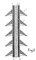
- FIG. 1 a longitudinal section through a composite insulator 1 is shown.
- a composite insulator 1 is the section of a long-rod insulator.
- a field control layer 3 is applied on a core 2 made of glass fiber reinforced plastic.
- it can have capacitive or resistive properties.
- it may contain ZnO microvaristors for resistive field control.
- the field control layer 3 is covered by a protective layer 4, which consists of an erosion and Kriechstromfesten material and the field control layer 3 protects against weathering and pollution.
- the screens 5 are arranged at regular intervals, which are injected from one of the known polymeric plastics.
- the field control layer 3 in a partial region of the insulator 1 consists of two layers 31 and 32, of which the layer 32 is arranged above the continuous layer 31.
- the two layers 31 and 32 may have different field control properties. So can the outer Layer 32 capacitive and the continuous layer 31 have resistive properties. Such an arrangement of the layers may be advantageous, for example, in the field of fittings in terms of constructive field disturbances.
- the field control layer 3 is uniformly thick throughout. In the area where the field control layer 3 is double-layered, by reducing the extrusion, the inner layer 31 can be thinned.
- the outer layer 32 can be applied so thick that a uniform, uniform layer thickness is achieved.
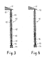
- FIGS. 3 and 4 show long-rod insulators 10, as used for example in high-voltage overhead lines.
- the structure of the field control layers of these insulators may for example correspond to the structure as in the in the FIGS. 1 or 2 is described insulators described.
- the insulators 10 each depend on a traverse 11 of a high-voltage mast, not shown here.
- the attachment takes place in a known manner with a fitting 12 made of metal.
- the conductor cables 14 are fastened by means of a further armature 13.
- the isolators 10 which are 4 meters in length, are only partially cut-off, as in FIG FIG. 3 represented, or only in a certain area on a fitting, as in FIG. 4 shown coated with a field control layer.
- the insulator 10 in FIG. 3 each has five equal areas 15 in which the core is covered with a field control layer. They are each interrupted by areas of equal size without field control layer.
- the insulator 10 in FIG. 4 has a portion 16 which is covered with a field control layer and which extends from the armature 13, to which the conductors 14 are attached, upwards over one third of the rod length.
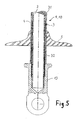
- FIG. 5 shows a schematic representation of a transition region from a fitting to the shield shell area in longitudinal section. It is a section through the end of an insulator with a fitting to which the conductors are attached, as in the Figures 3 or 4 is shown. Matching features with the Figures 2 . 3 and 4 are designated by the same reference numerals.
- the core consists of a rod 2 made of glass fiber reinforced plastic, which is coated with a field control layer 3, the in turn is enveloped by a protective layer 4. On this protective layer, the umbrellas 5 are raised.
- the field control layer 3 corresponds in structure to that as shown in FIG FIG. 2 is shown.
- the end of the rod 2 is enclosed by the fitting 13.
- a layer 31 completely covers the core 2 of the insulator on the length visible in the illustration. It is a layer with resistive effect and contains microvaristors.
- the capacitive field control is particularly suitable to reduce field strength peaks that are constructive, for example, by edges or stepped transitions, as they occur at the transition from a fitting to the insulator.
- To improve the conductive contact between the layers and the fitting of the core enclosing cavity of the fitting may be coated with a conductive paint. Also deposits of wire loops or wire nets are, as not shown, possible.
- FIG. 6 shows the result of a comparison test between a long-rod insulator whose surface corresponds to a field control layer FIG. 1 coated and a conventional long-rod insulator as reference insulator, which was equipped exclusively with HTV silicone without field control layer.
- the umbrellas were each made of HTV silicone. The striking distance was 2765 mm.
- a 3 mm thick polymer layer cross-sectional area: 1.8 cm 2 was applied to a GRP rod with a diameter of 16 mm.
- the polymer layer for field control were microvaristors, ZnO varistors in powder form, in a proportion of 50 to 90% by weight, preferably 70% by weight with a particle size of 10 nm to 100 ⁇ m, preferably between 0, 1 [mu] m and 10 [mu] m have been added.
- the filling level of the microvaristors was above the percolation limit, ie the microvaristors were in direct electrical contact with each other.
- FIG. 6 On the left are the isolator with field control layer and on the right the reference insulator during the comparison test. With an applied AC voltage of 750 kV (effective), the insulators were irrigated. While the reference insulator under the bottom five, the conductor side facing screens shows strong discharge activities, the equipped with the field control layer insulator is completely discharge-free.
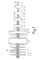
- Fig. 3 is a flow chart for explaining the manufacture of an insulator.
- the core 2 of the insulator to be produced is a rod which consists of a glass fiber reinforced plastic. This rod 2 is guided in the feed direction 20 by successively arranged stations, where it is completed to the insulator.
- a bonding agent 211 is applied so that the layers of the field control layer 3 to be subsequently applied are intimately joined to the core 2.
- a first layer 31 of the field control layer is applied, for example a layer with varistors, a layer with resistive character.
- another extruder 23 is provided for applying the further layer 32, for example a layer with a capacitive character.
- the next extruder 24 applies the protective layer 4.
- the insulator core can now be separated with a separating tool 25.
- the screens can be extruded or the already prefabricated umbrellas 5 are postponed.
- a thermal treatment 27 for curing the field control layer, the protective layer and the screens concludes the manufacture of the insulator 1; 10 off. After preparing the ends of the rod, the fittings can be attached to it.
Claims (19)
- Isolateur composite (1, 10) contenant un noyau (2) et une couche de protection (4) qui entoure le noyau (2), une couche de contrôle de champ (3) étant disposée entre le noyau (2) et la couche de protection (4) au moins dans une portion (15, 16) de l'isolateur (1, 10), laquelle contient en tant que matière de remplissage des particules qui influencent le champ électrique de l'isolateur,
caractérisé en ce
que la couche de contrôle de champ (3) comprend une strate (31, 32), la proportion de particules qui influencent le champ électrique étant différente sur la longueur de la strate (31, 32). - Isolateur composite (1, 10) selon la revendication 1, caractérisé en ce que la couche de contrôle de champ (3) se compose d'une, de deux strates (31, 32) ou plus et en ce que les strates (31, 32) individuelles possèdent des propriétés de contrôle de champ différentes.
- Isolateur composite (1, 10) selon la revendication 1 ou 2, caractérisé en ce que la couche de contrôle de champ (3) se compose d'une strate (31, 32) et contient comme masse de remplissage exclusivement des particules résistives ou capacitives.
- Isolateur composite (1, 10) selon l'une des revendications 1 ou 2, caractérisé en ce que la couche de contrôle de champ (3) se compose d'au moins deux strates (31, 32) et en ce que l'une des strates (31, 32) présente une proportion de particules résistives ou capacitives plus élevée que l'autre.
- Isolateur composite (1, 10) selon l'une des revendications 1 ou 2, caractérisé en ce que la couche de contrôle de champ (3) se compose d'au moins deux strates (31, 32) et en ce que l'une des strates (31) contient exclusivement des particules résistives et l'autre (32) exclusivement des particules capacitives.
- Isolateur composite (1, 10) selon l'une des revendications 1 ou 2, caractérisé en ce que la couche de contrôle de champ (3) se compose d'une strate (31, 32) et contient un mélange de particules résistives et capacitives.
- Isolateur composite (1, 10) selon l'une des revendications 1 ou 2, caractérisé en ce que la couche de contrôle de champ (3) se compose d'au moins deux strates (31, 32) et en ce que l'une des strates (31, 32) contient un mélange de particules résistives ou capacitives et l'autre couche (31, 32) exclusivement des particules résistives ou capacitives.
- Isolateur composite (1, 10) selon l'une des revendications 1 ou 7, caractérisé en ce que dans le cas de plusieurs strates (31, 32), les strates (31, 32) d'une couche de contrôle de champ (3) sont alternées les unes au-dessus des autres dans leur séquence et/ou composition en fonction de leur effet sur le champ électrique.
- Isolateur composite (1, 10) selon la revendication 8, caractérisé en ce que la proportion de particules capacitives et/ou résistives dans les strates (31, 32) individuelles de la couche (3) est différente.
- Isolateur composite (1, 10) selon l'une des revendications 1 ou 9, caractérisé en ce que la couche de contrôle de champ (3) est appliquées en portions (15) individuelles sur la longueur du noyau (2) de l'isolateur (10).
- Isolateur composite (1, 10) selon la revendication 10, caractérisé en ce que dans le cas d'une couche de contrôle de champ (3) qui est divisée en portions individuelles et qui se compose d'au moins deux strates (31, 32), dans la zone frontière avec la portion sans couche, une strate (31, 32) est plus longue que l'autre et s'étend au-delà de la strate (31, 32) qui se trouve au-dessus ou en-dessous de celle-ci jusqu'à la portion sans couche.
- Isolateur composite (1, 10) selon l'une des revendications 1 ou 11, caractérisé en ce que les strates (31, 32) individuelles de la couche de contrôle de champ (3) sont séparées les unes des autres par une strate en un matériau isolant.
- Isolateur composite (1, 10) selon l'une des revendications 1 à 12, caractérisé en ce que la proportion de particules dans une couche est comprise entre 50 et 90 % massiques, de préférence égale à 70 % massiques.
- Isolateur composite (1, 10) selon la revendication 13, caractérisé en ce que la proportion de particules, le taux de remplissage, est supérieur au seuil de percolation.
- Procédé de fabrication d'un isolateur composite (1, 10) contenant un noyau (2) et une couche de protection (4) qui entoure le noyau (2), selon l'une des revendications 1 à 14,
caractérisé en ce
que dans au moins une portion (15, 16) est appliquée sur le noyau (2) de l'isolateur (1, 10) une couche de contrôle de champ (3) constituée d'au moins une strate (31, 32) en un matériau élastomère qui présente une proportion de particules influençant le champ électrique de l'isolateur (1, 10) variable sur la longueur de la couche et en ce que l'ensemble du noyau (2) sur lequel a été appliquée la couche de contrôle de champ (3) est recouvert de la couche de protection (4) et en ce que l'isolateur (1, 10) est ensuite soumis à un traitement thermique (27) pour la vulcanisation des matières plastiques. - Procédé selon la revendication 15, caractérisé en ce que la couche de contrôle de champ (3) est appliquée en au moins deux strates (31, 32) ayant des effets différents sur le champ électrique.
- Procédé selon la revendication 15 ou 16, caractérisé en ce que la couche de contrôle de champ (3) est appliquée en portions (15) sur le noyau (2) de l'isolateur.
- Procédé selon la revendication 17, caractérisé en ce que dans le cas d'une couche de contrôle de champ (3) qui est divisée en portions individuelles et qui se compose d'au moins deux strates (31, 32), une strate (31, 32) est appliquée dans la zone frontière avec la portion sans couche au-dessus ou en-dessous de la strate (31, 32) qui se trouve au-dessus de celle-ci jusqu'à la portion sans couche.
- Procédé selon l'une des revendications 15 à 18, caractérisé en ce que l'apport de particules influençant le champ électrique de l'isolateur (1, 10) lors de l'application de la strate (31, 32) de la couche de contrôle de champ (3) sur le noyau (2)
s'effectue en quantités différentes vers le produit d'extrusion.
Priority Applications (2)
| Application Number | Priority Date | Filing Date | Title |
|---|---|---|---|
| PL09709505T PL2243145T3 (pl) | 2008-02-14 | 2009-02-12 | Izolator kompozytowy, sterowany polowo |
| SI200930550T SI2243145T1 (sl) | 2008-02-14 | 2009-02-12 | Kompozitni izolator za kontrolo električnega polja |
Applications Claiming Priority (2)
| Application Number | Priority Date | Filing Date | Title |
|---|---|---|---|
| DE102008009333A DE102008009333A1 (de) | 2008-02-14 | 2008-02-14 | Feldgesteuerter Verbundisolator |
| PCT/EP2009/000983 WO2009100904A1 (fr) | 2008-02-14 | 2009-02-12 | Isolateur composite à commande de champ |
Publications (2)
| Publication Number | Publication Date |
|---|---|
| EP2243145A1 EP2243145A1 (fr) | 2010-10-27 |
| EP2243145B1 true EP2243145B1 (fr) | 2013-01-23 |
Family
ID=40622154
Family Applications (1)
| Application Number | Title | Priority Date | Filing Date |
|---|---|---|---|
| EP09709505A Active EP2243145B1 (fr) | 2008-02-14 | 2009-02-12 | Isolateur composite à commande de champ |
Country Status (9)
| Country | Link |
|---|---|
| US (1) | US8637769B2 (fr) |
| EP (1) | EP2243145B1 (fr) |
| JP (1) | JP5302978B2 (fr) |
| CA (1) | CA2715651C (fr) |
| DE (2) | DE102008009333A1 (fr) |
| ES (1) | ES2401885T3 (fr) |
| PL (1) | PL2243145T3 (fr) |
| SI (1) | SI2243145T1 (fr) |
| WO (1) | WO2009100904A1 (fr) |
Families Citing this family (13)
| Publication number | Priority date | Publication date | Assignee | Title |
|---|---|---|---|---|
| CA2800273C (fr) | 2010-05-28 | 2017-10-03 | Lapp Insulators Gmbh | Isolateur composite |
| DE102010043995A1 (de) * | 2010-11-16 | 2012-05-16 | Siemens Aktiengesellschaft | Isolatoranordnung sowie Verfahren zur Herstellung einer Isolatoranordnung |
| DE102010043990A1 (de) * | 2010-11-16 | 2012-05-16 | Siemens Aktiengesellschaft | Isolatoranordnung sowie Verfahren zur Herstellung einer Isolatoranordnung |
| JP2012248525A (ja) * | 2011-05-31 | 2012-12-13 | Tokyo Electric Power Co Inc:The | ポリマーがいし |
| DE102011055401A1 (de) | 2011-11-16 | 2013-05-16 | Rwth Aachen | Isolierkörper und Verfahren zur Herstellung eines Isolierkörpers |
| DE102012104137A1 (de) * | 2012-05-11 | 2013-11-14 | Maschinenfabrik Reinhausen Gmbh | Feldgesteuerter Verbundisolator |
| EP3050184A4 (fr) * | 2013-09-25 | 2017-05-24 | 3M Innovative Properties Company | Compositions permettant la gradation d'un champ électrique |
| FR3057697B1 (fr) * | 2016-10-18 | 2020-02-14 | Sediver Sa | Isolateur pour lignes electriques aeriennes avec un detecteur de courant de fuite protege |
| JP6737407B2 (ja) * | 2017-07-13 | 2020-08-05 | 住友電気工業株式会社 | 非オーム性組成物およびその製造方法、ケーブル中間接続用ユニット並びにケーブル終端接続用ユニット |
| CA2989069A1 (fr) * | 2017-12-13 | 2019-06-13 | Hydro-Quebec | Composite, traverse enrobee du composite et leur utilisation dans un reseau electrique |
| EP3591672B1 (fr) * | 2018-07-02 | 2023-03-29 | Hitachi Energy Switzerland AG | Isolant a gradient de résistivité |
| EP3813082B1 (fr) * | 2019-10-21 | 2023-07-19 | Hitachi Energy Switzerland AG | Ailette d'isolateur ayant une pointe non circulaire |
| DE102022206149A1 (de) | 2022-06-21 | 2023-12-21 | Siemens Energy Global GmbH & Co. KG | Durchführungsisolator |
Family Cites Families (16)
| Publication number | Priority date | Publication date | Assignee | Title |
|---|---|---|---|---|
| DE1465287B2 (de) | 1964-05-14 | 1973-05-03 | Brown, Boveri & Cie Ag, 6800 Mannheim | Hochspannungsverbundisolator |
| DE1515467B2 (de) * | 1965-04-01 | 1971-04-15 | Brown, Boven & Cie AG, 6800 Mann heim | Hochspannungs verbundisolator |
| DE2006247A1 (de) | 1970-02-12 | 1971-10-07 | Jenaer Glaswerk Schott & Gen | Hochspannungsisolator |
| DD139962A3 (de) * | 1978-04-18 | 1980-01-30 | Manfred Kahle | Verfahren zur herstellung eines kunststoffisolators |
| DE3214141A1 (de) | 1982-04-14 | 1983-10-20 | Interpace Corp., Parsippany, N.J. | Polymer-stabisolator mit verbesserten stoerfeld- und corona-charakteristiken |
| NO167618C (no) * | 1989-03-20 | 1991-11-20 | Alcatel Stk As | Overspenningsavleder for elektriske apparater. |
| JP3602634B2 (ja) | 1996-01-09 | 2004-12-15 | 日本碍子株式会社 | 半導電性複合碍子 |
| SE510819C2 (sv) * | 1997-02-14 | 1999-06-28 | Ifoe Ceramics Ab | Elektrisk högspänningsisolator med ett halvledande ytskikt |
| DE19856123C2 (de) * | 1998-12-04 | 2000-12-07 | Siemens Ag | Hohlisolator |
| DE19858215C2 (de) | 1998-12-17 | 2003-07-24 | Ceramtec Ag | Verfahren und Vorrichtung zur Herstellung von Verbundisolatoren |
| GB0103255D0 (en) | 2001-02-09 | 2001-03-28 | Tyco Electronics Raychem Gmbh | Insulator arrangement |
| EP1337022A1 (fr) * | 2002-02-18 | 2003-08-20 | ABB Schweiz AG | Corps enveloppant pour un câble haute tension et élément de câble, qui est pourvu d'un tel corps enveloppant |
| ATE546818T1 (de) * | 2004-03-15 | 2012-03-15 | Abb Research Ltd | Hochspannungsdurchführung mit feldsteuermaterial |
| DE102005041167A1 (de) * | 2005-08-30 | 2007-03-01 | Obo Bettermann Gmbh & Co. Kg | Blitzstromableitvorrichtung |
| EP1870975B1 (fr) * | 2006-06-21 | 2010-08-04 | ABB Technology Ltd | Dispositif de commande de champ électrique |
| EP1936638A1 (fr) * | 2006-12-18 | 2008-06-25 | Abb Research Ltd. | Isolant électrique et son utilisation |
-
2008
- 2008-02-14 DE DE102008009333A patent/DE102008009333A1/de not_active Withdrawn
-
2009
- 2009-02-12 PL PL09709505T patent/PL2243145T3/pl unknown
- 2009-02-12 JP JP2010546261A patent/JP5302978B2/ja active Active
- 2009-02-12 DE DE202009018686U patent/DE202009018686U1/de not_active Expired - Lifetime
- 2009-02-12 SI SI200930550T patent/SI2243145T1/sl unknown
- 2009-02-12 WO PCT/EP2009/000983 patent/WO2009100904A1/fr active Application Filing
- 2009-02-12 ES ES09709505T patent/ES2401885T3/es active Active
- 2009-02-12 EP EP09709505A patent/EP2243145B1/fr active Active
- 2009-02-12 CA CA2715651A patent/CA2715651C/fr active Active
-
2010
- 2010-08-16 US US12/856,806 patent/US8637769B2/en active Active
Also Published As
| Publication number | Publication date |
|---|---|
| JP5302978B2 (ja) | 2013-10-02 |
| US8637769B2 (en) | 2014-01-28 |
| DE202009018686U1 (de) | 2012-11-06 |
| DE102008009333A1 (de) | 2009-08-20 |
| WO2009100904A1 (fr) | 2009-08-20 |
| CA2715651A1 (fr) | 2009-08-20 |
| SI2243145T1 (sl) | 2013-05-31 |
| EP2243145A1 (fr) | 2010-10-27 |
| PL2243145T3 (pl) | 2013-06-28 |
| CA2715651C (fr) | 2016-05-24 |
| ES2401885T3 (es) | 2013-04-25 |
| US20110017488A1 (en) | 2011-01-27 |
| JP2011514626A (ja) | 2011-05-06 |
Similar Documents
| Publication | Publication Date | Title |
|---|---|---|
| EP2243145B1 (fr) | Isolateur composite à commande de champ | |
| EP1476928B1 (fr) | Enveloppe pour cable haute tension, et element de cable muni d'une telle enveloppe | |
| EP0416452B1 (fr) | Câble pour électrofiltre | |
| EP1577904A1 (fr) | Traversée haute tension avec élément pour les contrôle du champ électrique | |
| AT507164B1 (de) | Elektrostatische abschirmung für einen hgü-bauteil | |
| DE2746870A1 (de) | Verfahren zur herstellung von freiluft-verbundisolatoren | |
| DE2436413A1 (de) | Hochspannungskabel | |
| EP1760855A1 (fr) | Dispositif de dérivation de courant de foudre | |
| EP3408856A1 (fr) | Bobine de self à air de type à transmission de courant continu haute tension et son procédé de fabrication | |
| EP2577685B1 (fr) | Isolateur composite | |
| EP2740197B1 (fr) | Dispositif conducteur électrique, dispositif anti-effluves terminal et procédé de production d'un dispositif anti-effluves terminal | |
| EP0068067B1 (fr) | Résistance à haute tension pour isolateurs de lignes aériennes | |
| DE1765602B1 (de) | Abriebfeste elektrische Leitung mit glatter Oberflaeche | |
| EP2715743A1 (fr) | Composant électrique pour installation haute tension | |
| DE102006056563B4 (de) | Distanzhalter zur Sicherstellung des Trennungsabstands für teilisolierte Blitzschutzanlagen | |
| DE602005005694T2 (de) | Hoch- oder mittelspannungsvorrichtung mit bestimmtem dielektrischem system | |
| EP3410451B1 (fr) | Anneau de protection pour une bobine de transformateur | |
| DE102017217163B4 (de) | Elektrisches Betriebsmittel und Herstellungsverfahren für ein elektrisches Betriebsmittel | |
| WO2020030753A1 (fr) | Matériau pour commander un champ électrique en fonction de la direction | |
| EP0779692A1 (fr) | Procédé de mise à la terre d'un écran d'un câble électrique ainsi que câble électrique | |
| DE102017212026A1 (de) | Schirmring und/oder Steigungsausgleich für eine Transformatorspule | |
| DE3214141A1 (de) | Polymer-stabisolator mit verbesserten stoerfeld- und corona-charakteristiken | |
| DE102012000125A1 (de) | Vorrichtung zur Verbesserung der elekrischen Eigenschaften einer Beschichtung eines Leiters oder dergleichen durch Isolierstoffe,sowie ein Verfahren zur Anwendung einer derartigen Vorrichtung | |
| CH170845A (de) | Verfahren für die Herstellung von Erzeugnissen mit gegeneinander isolierten elektrischen Leitern und nach diesem Verfahren hergestellter isolierter Leiter. | |
| DE1538405A1 (de) | UEberspannungsableiter |
Legal Events
| Date | Code | Title | Description |
|---|---|---|---|
| PUAI | Public reference made under article 153(3) epc to a published international application that has entered the european phase |
Free format text: ORIGINAL CODE: 0009012 |
|
| 17P | Request for examination filed |
Effective date: 20100908 |
|
| AK | Designated contracting states |
Kind code of ref document: A1 Designated state(s): AT BE BG CH CY CZ DE DK EE ES FI FR GB GR HR HU IE IS IT LI LT LU LV MC MK MT NL NO PL PT RO SE SI SK TR |
|
| AX | Request for extension of the european patent |
Extension state: AL BA RS |
|
| RIN1 | Information on inventor provided before grant (corrected) |
Inventor name: SEIFERT, JENS Inventor name: HINRICHSEN, VOLKER Inventor name: DENNDOERFER, HEINZ |
|
| DAX | Request for extension of the european patent (deleted) | ||
| GRAP | Despatch of communication of intention to grant a patent |
Free format text: ORIGINAL CODE: EPIDOSNIGR1 |
|
| GRAS | Grant fee paid |
Free format text: ORIGINAL CODE: EPIDOSNIGR3 |
|
| GRAA | (expected) grant |
Free format text: ORIGINAL CODE: 0009210 |
|
| AK | Designated contracting states |
Kind code of ref document: B1 Designated state(s): AT BE BG CH CY CZ DE DK EE ES FI FR GB GR HR HU IE IS IT LI LT LU LV MC MK MT NL NO PL PT RO SE SI SK TR |
|
| REG | Reference to a national code |
Ref country code: GB Ref legal event code: FG4D Free format text: NOT ENGLISH |
|
| REG | Reference to a national code |
Ref country code: CH Ref legal event code: EP |
|
| REG | Reference to a national code |
Ref country code: AT Ref legal event code: REF Ref document number: 595349 Country of ref document: AT Kind code of ref document: T Effective date: 20130215 Ref country code: CH Ref legal event code: EP |
|
| REG | Reference to a national code |
Ref country code: IE Ref legal event code: FG4D Free format text: LANGUAGE OF EP DOCUMENT: GERMAN |
|
| REG | Reference to a national code |
Ref country code: DE Ref legal event code: R096 Ref document number: 502009006099 Country of ref document: DE Effective date: 20130314 |
|
| REG | Reference to a national code |
Ref country code: CH Ref legal event code: NV Representative=s name: E. BLUM AND CO. AG PATENT- UND MARKENANWAELTE , CH |
|
| REG | Reference to a national code |
Ref country code: SE Ref legal event code: TRGR |
|
| REG | Reference to a national code |
Ref country code: RO Ref legal event code: EPE |
|
| REG | Reference to a national code |
Ref country code: ES Ref legal event code: FG2A Ref document number: 2401885 Country of ref document: ES Kind code of ref document: T3 Effective date: 20130425 |
|
| REG | Reference to a national code |
Ref country code: NL Ref legal event code: T3 |
|
| REG | Reference to a national code |
Ref country code: LT Ref legal event code: MG4D |
|
| REG | Reference to a national code |
Ref country code: PL Ref legal event code: T3 |
|
| PG25 | Lapsed in a contracting state [announced via postgrant information from national office to epo] |
Ref country code: IS Free format text: LAPSE BECAUSE OF FAILURE TO SUBMIT A TRANSLATION OF THE DESCRIPTION OR TO PAY THE FEE WITHIN THE PRESCRIBED TIME-LIMIT Effective date: 20130523 Ref country code: NO Free format text: LAPSE BECAUSE OF FAILURE TO SUBMIT A TRANSLATION OF THE DESCRIPTION OR TO PAY THE FEE WITHIN THE PRESCRIBED TIME-LIMIT Effective date: 20130423 Ref country code: LT Free format text: LAPSE BECAUSE OF FAILURE TO SUBMIT A TRANSLATION OF THE DESCRIPTION OR TO PAY THE FEE WITHIN THE PRESCRIBED TIME-LIMIT Effective date: 20130123 Ref country code: BG Free format text: LAPSE BECAUSE OF FAILURE TO SUBMIT A TRANSLATION OF THE DESCRIPTION OR TO PAY THE FEE WITHIN THE PRESCRIBED TIME-LIMIT Effective date: 20130423 |
|
| PG25 | Lapsed in a contracting state [announced via postgrant information from national office to epo] |
Ref country code: FI Free format text: LAPSE BECAUSE OF FAILURE TO SUBMIT A TRANSLATION OF THE DESCRIPTION OR TO PAY THE FEE WITHIN THE PRESCRIBED TIME-LIMIT Effective date: 20130123 Ref country code: GR Free format text: LAPSE BECAUSE OF FAILURE TO SUBMIT A TRANSLATION OF THE DESCRIPTION OR TO PAY THE FEE WITHIN THE PRESCRIBED TIME-LIMIT Effective date: 20130424 Ref country code: LV Free format text: LAPSE BECAUSE OF FAILURE TO SUBMIT A TRANSLATION OF THE DESCRIPTION OR TO PAY THE FEE WITHIN THE PRESCRIBED TIME-LIMIT Effective date: 20130123 Ref country code: PT Free format text: LAPSE BECAUSE OF FAILURE TO SUBMIT A TRANSLATION OF THE DESCRIPTION OR TO PAY THE FEE WITHIN THE PRESCRIBED TIME-LIMIT Effective date: 20130523 |
|
| BERE | Be: lapsed |
Owner name: LAPP INSULATORS G.M.B.H. Effective date: 20130228 |
|
| PG25 | Lapsed in a contracting state [announced via postgrant information from national office to epo] |
Ref country code: HR Free format text: LAPSE BECAUSE OF FAILURE TO SUBMIT A TRANSLATION OF THE DESCRIPTION OR TO PAY THE FEE WITHIN THE PRESCRIBED TIME-LIMIT Effective date: 20130123 Ref country code: MC Free format text: LAPSE BECAUSE OF NON-PAYMENT OF DUE FEES Effective date: 20130228 |
|
| PG25 | Lapsed in a contracting state [announced via postgrant information from national office to epo] |
Ref country code: DK Free format text: LAPSE BECAUSE OF FAILURE TO SUBMIT A TRANSLATION OF THE DESCRIPTION OR TO PAY THE FEE WITHIN THE PRESCRIBED TIME-LIMIT Effective date: 20130123 Ref country code: SK Free format text: LAPSE BECAUSE OF FAILURE TO SUBMIT A TRANSLATION OF THE DESCRIPTION OR TO PAY THE FEE WITHIN THE PRESCRIBED TIME-LIMIT Effective date: 20130123 Ref country code: CZ Free format text: LAPSE BECAUSE OF FAILURE TO SUBMIT A TRANSLATION OF THE DESCRIPTION OR TO PAY THE FEE WITHIN THE PRESCRIBED TIME-LIMIT Effective date: 20130123 Ref country code: EE Free format text: LAPSE BECAUSE OF FAILURE TO SUBMIT A TRANSLATION OF THE DESCRIPTION OR TO PAY THE FEE WITHIN THE PRESCRIBED TIME-LIMIT Effective date: 20130123 |
|
| REG | Reference to a national code |
Ref country code: HU Ref legal event code: AG4A Ref document number: E017493 Country of ref document: HU |
|
| PG25 | Lapsed in a contracting state [announced via postgrant information from national office to epo] |
Ref country code: CY Free format text: LAPSE BECAUSE OF FAILURE TO SUBMIT A TRANSLATION OF THE DESCRIPTION OR TO PAY THE FEE WITHIN THE PRESCRIBED TIME-LIMIT Effective date: 20130123 |
|
| PLBE | No opposition filed within time limit |
Free format text: ORIGINAL CODE: 0009261 |
|
| STAA | Information on the status of an ep patent application or granted ep patent |
Free format text: STATUS: NO OPPOSITION FILED WITHIN TIME LIMIT |
|
| REG | Reference to a national code |
Ref country code: IE Ref legal event code: MM4A |
|
| 26N | No opposition filed |
Effective date: 20131024 |
|
| PG25 | Lapsed in a contracting state [announced via postgrant information from national office to epo] |
Ref country code: BE Free format text: LAPSE BECAUSE OF NON-PAYMENT OF DUE FEES Effective date: 20130228 Ref country code: IE Free format text: LAPSE BECAUSE OF NON-PAYMENT OF DUE FEES Effective date: 20130212 |
|
| REG | Reference to a national code |
Ref country code: DE Ref legal event code: R097 Ref document number: 502009006099 Country of ref document: DE Effective date: 20131024 |
|
| PG25 | Lapsed in a contracting state [announced via postgrant information from national office to epo] |
Ref country code: MT Free format text: LAPSE BECAUSE OF FAILURE TO SUBMIT A TRANSLATION OF THE DESCRIPTION OR TO PAY THE FEE WITHIN THE PRESCRIBED TIME-LIMIT Effective date: 20130123 |
|
| PG25 | Lapsed in a contracting state [announced via postgrant information from national office to epo] |
Ref country code: LU Free format text: LAPSE BECAUSE OF NON-PAYMENT OF DUE FEES Effective date: 20130212 Ref country code: MK Free format text: LAPSE BECAUSE OF FAILURE TO SUBMIT A TRANSLATION OF THE DESCRIPTION OR TO PAY THE FEE WITHIN THE PRESCRIBED TIME-LIMIT Effective date: 20130123 |
|
| REG | Reference to a national code |
Ref country code: FR Ref legal event code: PLFP Year of fee payment: 8 |
|
| REG | Reference to a national code |
Ref country code: FR Ref legal event code: PLFP Year of fee payment: 9 |
|
| REG | Reference to a national code |
Ref country code: FR Ref legal event code: PLFP Year of fee payment: 10 |
|
| PGFP | Annual fee paid to national office [announced via postgrant information from national office to epo] |
Ref country code: FR Payment date: 20230217 Year of fee payment: 15 |
|
| PGFP | Annual fee paid to national office [announced via postgrant information from national office to epo] |
Ref country code: TR Payment date: 20230209 Year of fee payment: 15 Ref country code: SE Payment date: 20230220 Year of fee payment: 15 Ref country code: PL Payment date: 20230127 Year of fee payment: 15 Ref country code: IT Payment date: 20230228 Year of fee payment: 15 |
|
| PGFP | Annual fee paid to national office [announced via postgrant information from national office to epo] |
Ref country code: NL Payment date: 20240220 Year of fee payment: 16 Ref country code: ES Payment date: 20240319 Year of fee payment: 16 |
|
| PGFP | Annual fee paid to national office [announced via postgrant information from national office to epo] |
Ref country code: AT Payment date: 20240216 Year of fee payment: 16 |
|
| PGFP | Annual fee paid to national office [announced via postgrant information from national office to epo] |
Ref country code: RO Payment date: 20240202 Year of fee payment: 16 Ref country code: HU Payment date: 20240206 Year of fee payment: 16 Ref country code: DE Payment date: 20240228 Year of fee payment: 16 Ref country code: GB Payment date: 20240222 Year of fee payment: 16 Ref country code: CH Payment date: 20240301 Year of fee payment: 16 |
|
| PGFP | Annual fee paid to national office [announced via postgrant information from national office to epo] |
Ref country code: SI Payment date: 20240130 Year of fee payment: 16 |