EP2240962B1 - Schutz vor elektrostatischen entladungen - Google Patents
Schutz vor elektrostatischen entladungen Download PDFInfo
- Publication number
- EP2240962B1 EP2240962B1 EP08872032.1A EP08872032A EP2240962B1 EP 2240962 B1 EP2240962 B1 EP 2240962B1 EP 08872032 A EP08872032 A EP 08872032A EP 2240962 B1 EP2240962 B1 EP 2240962B1
- Authority
- EP
- European Patent Office
- Prior art keywords
- coupled
- esd
- terminal
- esd clamp
- circuit
- Prior art date
- Legal status (The legal status is an assumption and is not a legal conclusion. Google has not performed a legal analysis and makes no representation as to the accuracy of the status listed.)
- Active
Links
Images

Classifications
-
- H—ELECTRICITY
- H02—GENERATION; CONVERSION OR DISTRIBUTION OF ELECTRIC POWER
- H02H—EMERGENCY PROTECTIVE CIRCUIT ARRANGEMENTS
- H02H9/00—Emergency protective circuit arrangements for limiting excess current or voltage without disconnection
- H02H9/04—Emergency protective circuit arrangements for limiting excess current or voltage without disconnection responsive to excess voltage
- H02H9/045—Emergency protective circuit arrangements for limiting excess current or voltage without disconnection responsive to excess voltage adapted to a particular application and not provided for elsewhere
- H02H9/046—Emergency protective circuit arrangements for limiting excess current or voltage without disconnection responsive to excess voltage adapted to a particular application and not provided for elsewhere responsive to excess voltage appearing at terminals of integrated circuits
Definitions
- the present invention generally relates to electrostatic discharge (ESD) protection of electronic elements and, more particularly, ESD protection of semiconductor components and integrated circuits.
- ESD electrostatic discharge
- Modem electronic devices especially semiconductor (SC) devices and integrated circuits (ICs) are at risk of damage due to electrostatic discharge (ESD) events.
- ESD electrostatic discharge
- SC devices and ICs semiconductor devices and integrated circuits
- I/O input/output
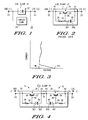
- ESD clamp 21 is placed between input/output (I/O) terminals 22 and ground or common terminal 23 of a SC device or IC to protect the other devices on the chip, that is, to protect circuit core 24 which is also coupled to I/O terminals 22 and common (e.g., "GND") terminal 23.
- Zener diode symbol 21' within ESD clamp 21 indicates that the function of ESD clamp 21 is to limit the voltage than can appear across circuit core 24 irrespective of the voltage applied to external terminals 22, 23.
- the abbreviation "GND" is intended to refer to the common or reference terminal of a particular circuit or electronic element, irrespective of whether it is actually coupled to an earth return.
- FIG. 2 is a simplified schematic diagram illustrating internal components of prior art ESD clamp 31 which is inserted in circuit 20 in place of ESD clamp 21.
- ESD clamp 31 comprises bipolar transistor 25, having emitter 26, collector 27 and base 28, resistance 29 and Zener diode 30 having terminals 301, 302.
- Resistance 29 includes the inherent resistance of the base region of transistor 25 and any discrete resistance provided external to transistor 25. In some applications it is common to externally directly connect the base and emitter contacts in which case resistance 29 represents the inherent base resistance and any small contact resistance. The purpose of resistance 29 (and analogous resistances 29, 39, 39' in FIGS.
- FIG. 3 is an illustration of a typical current-voltage characteristic of an ESD clamp, where voltage Vt1 is referred to as the trigger voltage and voltage Vh is referred to as the holding voltage.
- US2007/0258176 (Ball et al. ), against which the preamble is based on, describes a protection device.
- a shunt protection circuit is arranged in parallel to a circuit being protected.
- the circuit being protected may be an LED.
- the shunt protection circuit includes a pair of back-to-back diodes, a resistor and a MOS gated SCR.
- the shunt protection circuit can provide an alternative current flow path around the LED, if the LED fails in an open circuit condition.
- HBM testing is intended to replicate the ESD transients encountered in the real world when the electronic device is touched by a charged human being.
- CDM testing is intended to better replicate the conditions in the real world where the component itself (e.g., the SC device or IC) may become charged, thus causing an ESD event.
- HBM testing is the oldest and most commonly used ESD evaluation method and typically involves subjecting the device under test (DUT) to pulses having a rise time of the order of 10 nanoseconds.
- CDM testing subjects the DUT to transients with a rise-time of the order of 100 picoseconds or less, which is two orders of magnitude faster than that encountered during HBM testing.
- the differences in pulse rise times for CDM and HBM tests reflect the differences in real-world ESD events arising from such different causes. It has been found that the response of ESD protection elements such as that illustrated in FIG. 2 can vary significantly and in unpredictable ways depending upon the rise-time of the stress transient.
- FIG. 4 is a simplified schematic diagram illustrating internal components of ESD clamp 41, according to an example of the present invention.
- ESD clamp 41 is used in generalized protection circuit 20 in place of ESD clamp 21.
- ESD clamp 41 differs from prior art ESD clamp 31 of FIG. 2 in that it utilizes two series coupled transistor stages T1 and T2 joined in mirror configuration at node 52.
- Transistor stage T1 comprises transistor 25 analogous to transistor 25 of FIG. 2 with emitter 26, collector 27 and base 28, plus resistance 29 and Zener diode 30, coupled in generally the same manner as in FIG. 2 .
- the same reference numbers are used for transistor stage T1 and ESD clamp 31 of FIG. 2 to indicate that the individual elements are analogous but not necessarily identical.
- Resistor 29 is coupled between base 28 at node 34 and emitter 26 at node 32.
- Node 32 is adapted to be coupled to GND terminal 23 of ESD protection circuit 20 of FIG. 1 .
- Zener diode 30 is coupled between base 28 at node 34 and collector 27 at node 33.
- Node 33 is adapted to be coupled to node 43 of transistor stage T2 via node 52.
- Transistor stage T2 comprises transistor 35 analogous to transistor 25 of stage T1.
- Transistor 35 comprises emitter 36, collector 37 and base 38.
- Resistance 39 is coupled between base 38 at node 44 and emitter 36 at node 42.
- Zener diode 40 is coupled between base 38 at node 44 and collector 37 at node 43.
- Node 43 of Transistor stage T2 is coupled to node 33 of transistor stage T1 via node 52 in mirror configuration, collector 27 coupled to collector 37.
- Nodes 33, 52 and 43 are shown as separate nodes merely for convenience of description and can be combined.
- Node 42 of Transistor stage T2 is adapted to be coupled to input/output (I/O) terminals 22 of ESD circuit 20 of FIG. 1 .
- stages T1 and T2 of ESD clamp 4] individually resemble ESD clamp 31 of FIG. 2 , that they are serially coupled in opposition, that is, node 43 of stage T2 is coupled to node 33 of stage T1, or to say it another way, collector 27 of stage T1 is coupled to collector 37 of stage T2 via common node 52.
- ESD clamp 41 is bi-directional, that is, it will respond, for example, to a positive going ESD transient at either of terminals 22 or 23 of ESD circuit 20. This is a significant advantage since it results in a substantial area saving in providing bi-directional ESD protection to circuit core 24, and thereby lowers the cost of manufacture of the SC device or IC containing circuit core 24 (see FIG. 1 ).
- FIG. 5 is a simplified schematic diagram illustrating internal components of ESD clamp 51 according to a further example of the present invention, wherein it will be understood that clamp 51 is substituted for clamp 21 in generalized ESD protection circuit 20 of FIG. 1 .
- ESD clamp 51 differs from ESD clamp 41 of FIG. 4 in that it comprises two serially coupled ESD stages, that is, lower ESD stage or clamp 41 and upper ESD stage or clamp 41'.
- lower and upper are used herein merely to indicate that one of the pair of serially coupled ESD stages (e.g., clamp 41) is coupled to so-called GND terminal 23 of ESD circuit 20 and the other of the pair of serially coupled ESD stages (e.g., clamp 41') is coupled to so-called I/O terminals 22 of ESD circuit 20 of FIG. 1 , wherein GND is usually (but not always) the lower potential side of circuit 20 and the I/O terminals are coupled to what is usually (but not always) the higher potential side of ESD circuit 20.
- GND is usually (but not always) the lower potential side of circuit 20
- I/O terminals are coupled to what is usually (but not always) the higher potential side of ESD circuit 20.
- the designations of "lower” and “upper” are merely for convenience of reference and not intended to be limiting. Lower ESD stage or clamp 41 is described in connection with FIG. 4 .
- Upper ESD stage or clamp 41' is analogous to lower ESD stage or clamp 41 and the convention is adopted of identifying the individual components thereof analogous to those of lower ESD stage or clamp 41 by adding a prime to the individual reference numbers, for example, emitter 26' of upper ESD stage or clamp 41' is analogous to emitter 26 of lower ESD stage or clamp 41, collector 27' to collector 27, and so forth.
- ESD stages or clamps 41, 41' are coupled so that: (i) node 42 of lower stage or clamp 41 is coupled to node 32' of upper stage or clamp 41'; (2) bottom node 32 of lower stage or clamp 41 is adapted to be coupled to GND terminal 23 of ESD circuit 20; and (iii) top node 42' of upper stage or clamp 41' is adapted to be coupled to I/O terminals 22 of ESD circuit 20.
- stacked ESD clamps comprise serially coupled (i.e., “stacked") arrangements of lower ESD stage or clamp 41 and upper ESD stage or clamp 41', wherein the bottom node (e.g., node 32) of the stack is adapted to be coupled to GND terminal 23 and the top node of the stack (e.g., node 42') is adapted to be coupled to I/O terminal 22 of ESD circuit 20 of FIG. 1 , and intermediate nodes 42, 32' are coupled together at node 65.
- Nodes 42, 32 and 65 are shown as separate nodes merely for convenience of description and can be combined.
- Such a multiple "stacked" arrangement makes it possible to obtain higher trigger voltages and holding voltages (e.g., voltage Vt1 amd Vh of FIG. 3 ) than are generally possible with a single ESD protection stage, such as is illustrated in FIG. 4 .
- FIG. 6 is a simplified schematic diagram illustrating internal components of ESD clamp 61 according to an embodiment of the present invention, wherein it will be understood that clamp 61 is substituted for clamp 21 in ESD circuit 20 of FIG. 1 .
- ESD clamp 61 of FIG. 6 differs from ESD clamp 51 of FIG. 5 by the addition of RC ladder 60 comprising resistances R1, R2, R3, R4, etc., and capacitances C1, C2, C3, etc.
- RC ladder 60 has a first terminal of resistance R1 coupled to node 32 (e.g., emitter 26) of first ESD stage or clamp 41, a first terminal of resistance R2 coupled to interior node 52 (e.g., collectors 27, 37) of first ESD stage or clamp 41, a first terminal of resistance R3 coupled to coupling node 65 (e.g., emitters 36, 26') between ESD stages or clamps 41, 41'.
- node 32 e.g., emitter 26
- R2 coupled to interior node 52 (e.g., collectors 27, 37) of first ESD stage or clamp 41
- R3 coupled to coupling node 65 (e.g., emitters 36, 26') between ESD stages or clamps 41, 41'.
- a first terminal of resistance R4 is coupled to interior node 52' (e.g., collectors 27', 37') of second ESD stage or clamp 41' and, in a still further embodiment, a first terminal of resistor R5 is coupled to terminal node 42', (e.g., emitter 36') of second ESD stage or clamp 41'.
- Capacitance C1 is coupled between the second terminals of resistances R1 and R2
- capacitance C2 is coupled between the second terminals of resistances R2 and R3 and, when utilized in the further embodiment, capacitance C3 is coupled between the second terminals of resistances R3 and R4, and when utilized in still further embodiments, capacitance C4 is coupled between second terminals of resistances R4 and R5.
- resistances R4, R5 and associated capacitances C3, C4 may be included in some embodiments but omitted in other embodiments. While including one or both of resistances R4, R5 and associated capacitances C3, C4 is desirable, they are not essential. If capacitance C4 is included it should be robust, that is, able to withstand by itself the full operating voltage of circuit core 24 that ESD clamp 61 of FIG. 6 is intended to protect. The same consideration applies to ESD clamp 71 of FIG. 7 if C4 is included therein.
- ESD clamps 51, 61, 71 of FIG. 5-7 are shown as comprising two stacked bidirectional ESD stages 41, 41', but persons of skill in the art will understand based on the explanation herein, that that any number N of such stages may be stacked, by serially coupling N such stages 41, 41', 41" ... etc., if it is desired to achieve to higher trigger voltages.
- the individual stages of the stack e.g., 41, 41', 41", etc.
- the total number of resistances and capacitances included in RC ladder 60 can also be increased, depending upon the total number of stacked stages.
- N ESD clamp stages are provided with a first terminal of resistances R1, R2, R3, ... etc., coupled to every node thereof (e.g., nodes 32, 52, 65 (42, 33'), 52', 42' etc.) and capacitances C1, C2, ...etc., coupled between second terminals of the successive resistances of RC ladder 60, there will be 2N+1 resistances and 2N capacitances in RC ladder 60. However, not all such resistances and capacitances are necessary and some may be omitted.
- resistance R 2N+1 having a first terminal coupled to the second (upper) terminal node (e.g., node 42') of the N th ESD clamp stage and capacitor C 2N coupled between a second terminal of resistance R 2N+1 and a second terminal of resistance R 2N coupled to the interior node of the N th ESD clamp stage, may be omitted.
- resistance R 2N+1 and resistance R 2N and capacitances C 2N and C 2N-1 may all be omitted, where resistance R 2N would have had a first terminal thereof coupled to the interior node of the N th ESD clamp stage, resistance R 2N-1 would have a first terminal coupled to the first or lower node (e.g., node 32') of the Nth ESD clamp stage, and capacitance C 2N-1 would have been coupled between the second terminal of R 2N and R 2N-1 .
- RC ladder 60 is useful in reducing the sensitivity of ESD clamps 61, 71 to the rise time of the ESD signal.
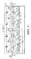
- FIG. 7 is a simplified schematic diagram illustrating internal components of ESD clamp 71 according to a further embodiment of the present invention, wherein it will be understood that clamp 71 is substituted for clamp 21 in ESD circuit 20 of FIG. 1 .
- ESD clamp 71 of FIG. 7 differs from ESD clamp 61 of FIG. 6 in that diode D1 is coupled between node 32 of lower ESD stage or clamp 41 and node 65 between lower ESD stage or clamp 41 and upper ESD stage or clamp 41'. Inclusion of Diode D1 has the advantage of providing asymmetric trigger voltages.
- the ESD clamp trigger voltage (e.g., Vtl+) is determined by the combined effect of both ESD stages or clamps 41, 41', that is, by all four ESD transistor stages T1, T2, T1', T2'.
- diode D1 effectively bypasses ESD stage or clamp 41, that is, bypasses transistor stages T1, T2, so that the trigger voltage (e.g., Vt1-) is determined substantially only by upper ESD stage or clamp 41', that is, by transistor stages T1', T2'.
- diode D1 is shown as being coupled between nodes 32 and 65, this is merely for convenience of explanation and not intended to be limiting. D1 or an equivalent diode may be coupled between other nodes of stacked ESD clamp 71 and in other orientations, depending upon relative trigger voltages desired for various polarities of the ESD transient and the total number of stacked stages.
- stacked ESD clamps 51, 61, 71 are shown as comprising two stacked ESD stages (e.g., ESD stages or clamps 41, 41'), this is merely for convenience of explanation and not intended to be limiting, and it will be understood by those of skill in the art, that more or fewer stages may also be used. This is also true of RC ladder 60 of FIGS. 6 and 7 , in that more or fewer RC ladder stages may be utilized for any given number of ESD stages as well as being varied to accommodate different numbers of ESD stages.
- Table I below illustrates the comparative results of using transmission line pulse testing (mimicking HBM) and very fast transmission line pulse testing (mimicking CDM) to evaluate the performance of different ESD protection arrangements.
- the HBM transients had pulse widths of about 100 nanoseconds with rise times of between 1 and 10 nanoseconds and the CDM transients had pulse widths of about 1 nanosecond with rise times of the order of 100 picoseconds.
- the HBM tests subjected the device under test to a maximum voltage of about 250 volts and pulse current limits of about 10 amps.
- the CDM tests subjected the device under test to a maximum voltage of about 500 volts and pulse current limit of about 20 amps.
- the device under test employed the ESD clamp configuration shown in FIG.
- inclusion of RC ladder 60 provides overall improved consistency and predictability of the Vt1 and Vh values for the ESD clamp.
- RC ladder 60 In addition to providing improved performance, the inclusion of RC ladder 60 also makes it easier to predetermine the ESD clamp trigger voltage Vt1, which is a great convenience in designing for optimum protection, especially for high voltage, high power components or ICs.
- Other elements of ESD clamps 61, 71 of FIGS. 6 and 7 were substantially the same with only the respective RC ladder values differing from test to test.
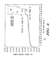
- FIG. 8 shows plot 75 of leakage current in amps versus DC applied voltage in volts, illustrating that the safe operating area is improved for a device with ESD protection according to embodiments of the present invention including RC ladder 60.
- Trace 80 shows the response of circuit 20 using ESD clamp 71 of FIG. 7 but without RC ladder 60 and trace 82 shows the response of substantially the same clamp but with RC ladder 60 comprising resistances R1, R2, R3, R4 and capacitances C1, C2, C3 included. It will be noted that substantially higher DC voltages can be applied before the leakage current becomes significant.
- the current scale of FIG. 8 is logarithmic, that is, each division of the scale corresponds to an order of magnitude increase in current. The result is a substantial increase in safe operating area, which is approximately given by area 84 between the rapidly rising portions of traces 80 and 82.
Landscapes
- Engineering & Computer Science (AREA)
- Microelectronics & Electronic Packaging (AREA)
- Semiconductor Integrated Circuits (AREA)
- Emergency Protection Circuit Devices (AREA)
- Tone Control, Compression And Expansion, Limiting Amplitude (AREA)
Claims (13)
- Ein elektrostatische Entladung, ESD, Schutzschaltkreis (61), welcher einen Eingabe/Ausgabe, I/O, Anschluss (22) und einen gemeinsamen Anschluss (23) hat, welcher angepasst ist, einen Schaltkreiskern (24) zu schützen, welcher zwischen dem I/O Anschluss und dem gemeinsamen Anschluss gekoppelt ist und welcher dadurch gekennzeichnet ist, dass er aufweist:mehrere in Reihe angeordnete ESD Klemmstufen (41, 41'), welche zwischen dem I/O Anschluss und dem gemeinsamen Anschluss gekoppelt sind; undeine Widerstand - Kondensator, RC, Leiter (60) parallel zu mindestens einem Teil der mehreren in Reihe angeordneten ESD Klemmstufen undmit Widerständen (R1, R2, R3, R4, R5) der RC Leiter, welche an Knoten (32, 33, 42, 43, 32', 33', 42', 43') der in Reihe angeordneten ESD Klemmstufen gekoppelt sind; wobeidie RC Leiter aufweist einen ersten Widerstand (R1), einen zweiten Widerstand (R2) und einen dritten Widerstand (R3) und einen ersten Kondensator (C1) und einen zweiten Kondensator (C2), wobeiein erster Anschluss des ersten Widerstands (R1) an einen ersten Knoten (32) eines ersten Anschlusses einer ESD Klemmstufe (41) der in Reihe angeordneten ESD Klemmstufen gekoppelt ist,ein erster Anschluss des zweiten Widerstands (R2) an einen zweiten Knoten (52) intern an die ESD Klemmstufe gekoppelt ist, undein erster Anschluss des dritten Widerstands (R3) an einen dritten Knoten (65) gekoppelt ist, welcher an einen zweiten Anschluss der ESD Klemmstufe gekoppelt ist, wobei der erste Kondensator (C1) zwischen einen zweiten Anschluss des ersten Widerstands und einen zweiten Anschluss des zweiten Widerstands gekoppelt ist, und der zweite Kondensator (C2) zwischen den zweiten Anschluss des zweiten Widerstands und einen zweiten Anschluss des dritten Widerstands gekoppelt ist.
- Der Schaltkreis gemäß Anspruch 1, wobei
die mehreren in Reihe angeordneten ESD Klemmstufen eine zweite ESD Klemmstufe (41') aufweisen und
die Knoten einen vierten Knoten (52') intern an der zweiten ESD Klemmstufe und einen fünften Knoten (42') an einem Endanschluss der zweiten ESD Klemmstufe aufweisen, wobei der erste Knoten an den gemeinsamen Anschluss gekoppelt ist und der fünfte Knoten an den I/O Anschluss gekoppelt ist, wobei
der dritte Knoten (65) den zweiten Anschluss der ESD Klemmstufe an einen ersten Anschluss der zweiten ESD Klemmstufe (41') in Reihe koppelt. - Der Schaltkreis gemäß Anspruch 1 oder 2, ferner aufweisend
eine Diode (30, 40), welche zwischen den ersten Knoten und den dritten Knoten gekoppelt ist. - Der Schaltkreis gemäß einem der Ansprüche 1 bis 3, ferner aufweisend einen vierten Widerstand (R4) und einen dritten Kondensator (C3), wobei der vierte Widerstand einen ersten Anschluss von sich an den vierten Knoten (52') gekoppelt hat, und
der dritte Kondensator zwischen den zweiten Anschluss des dritten Widerstands (R3) und einen zweiten Anschluss des vierten Widerstands gekoppelt ist. - Der Schaltkreis gemäß einem der Ansprüche 1 bis 4, ferner aufweisend einen fünften Widerstand (R5) und einen vierten Kondensator (C4), wobei der fünfte Widerstand einen ersten Anschluss von sich an den fünften Knoten (42') gekoppelt hat und
der vierte Kondensator zwischen den zweiten Anschluss des vierten Widerstands und einen zweiten Anschluss des fünften Widerstands gekoppelt ist. - Der Schaltkreis gemäß einem beliebigen der vorangehenden Ansprüche, wobei mindestens einige der mehreren in Reihe angeordneten ESD Klemmstufen bidirektional sind.
- Der Schaltkreis gemäß Anspruch 6, ferner aufweisend
eine Diode (30, 40, 30', 40'), welche über mindestens eine der mehreren in Reihe angeordneten bidirektionalen ESD Klemmstufen gekoppelt ist. - Der Schaltkreis gemäß Anspruch 7, wobei
die Diode eine Zener-Diode ist. - Der Schaltkreis gemäß Anspruch 1, wobei
die Widerstände (R1, R2, R3, R4, R5) der RC Leiter (60) im Wesentlichen ähnliche Werte haben und
die Kondensatoren (C1, C2, C3, C4) der RC Leiter im Wesentlichen ähnliche Werte haben. - Der Schaltkreis gemäß einem beliebigen der vorangehenden Ansprüche, wobei jede ESD Klemmstufe (41, 41') aufweist
eine erste Transistorstufe (T1, T1') und eine zweite Transistorstufe (T2, T2'), welche in Reihe in Spiegelkonfiguration gekoppelt sind, wobei
jede Transistorstufe einen Emitter (26, 26', 36, 36'), eine Basis (28, 28', 38, 38') und einen Kollektor (27, 27', 37, 37') hat, und wobei
der innere Knoten (52, 52') jeder ESD Klemmstufe den Kollektor der ersten Transistorstufe und den Kollektor der zweiten Transistorstufe koppelt. - Der Schaltkreis gemäß Anspruch 10, wobei
Emitter (26, 26', 36, 36') der ersten Transistorstufe (T1, T1') und der zweiten Transistorstufe (T2, T2') jeweils an den ersten Anschlussknoten (32, 32') und den zweiten Anschlussknoten (42, 42') von jeder der ESD Klemmstufen gekoppelt sind. - Der Schaltkreis gemäß Anspruch 10 oder 11, ferner aufweisend eine Zener Diode (30, 30', 40, 40'), welche zwischen den Kollektor und die Basis jeder Transistorstufe gekoppelt ist.
- Der Schaltkreis gemäß Anspruch 10 bis 12, wobei
ein Emitter (26) der ersten Transistorstufe (T1) einer ersten der N ESD Klemmstufen (41) an den gemeinsamen Anschluss (23) gekoppelt ist, und
ein Emitter (36') der zweiten Transistorstufe (T2') der Nten ESD Klemmstufe (41') an die I/O Anschlüsse (22) gekoppelt ist.
Applications Claiming Priority (2)
| Application Number | Priority Date | Filing Date | Title |
|---|---|---|---|
| US12/023,181 US7701682B2 (en) | 2008-01-31 | 2008-01-31 | Electrostatic discharge protection |
| PCT/US2008/088627 WO2009099500A2 (en) | 2008-01-31 | 2008-12-31 | Electrostatic discharge protection |
Publications (3)
| Publication Number | Publication Date |
|---|---|
| EP2240962A2 EP2240962A2 (de) | 2010-10-20 |
| EP2240962A4 EP2240962A4 (de) | 2011-09-28 |
| EP2240962B1 true EP2240962B1 (de) | 2016-10-26 |
Family
ID=40931446
Family Applications (1)
| Application Number | Title | Priority Date | Filing Date |
|---|---|---|---|
| EP08872032.1A Active EP2240962B1 (de) | 2008-01-31 | 2008-12-31 | Schutz vor elektrostatischen entladungen |
Country Status (4)
| Country | Link |
|---|---|
| US (1) | US7701682B2 (de) |
| EP (1) | EP2240962B1 (de) |
| CN (1) | CN101926004B (de) |
| WO (1) | WO2009099500A2 (de) |
Families Citing this family (17)
| Publication number | Priority date | Publication date | Assignee | Title |
|---|---|---|---|---|
| US7075720B2 (en) | 2002-08-22 | 2006-07-11 | Asml Netherlands B.V. | Structures and methods for reducing polarization aberration in optical systems |
| US8390092B2 (en) | 2010-11-12 | 2013-03-05 | Freescale Semiconductor, Inc. | Area-efficient high voltage bipolar-based ESD protection targeting narrow design windows |
| US8982516B2 (en) | 2010-11-12 | 2015-03-17 | Freescale Semiconductor, Inc. | Area-efficient high voltage bipolar-based ESD protection targeting narrow design windows |
| US8885309B2 (en) | 2011-03-24 | 2014-11-11 | Fairchild Semiconductor Corporation | Undervoltage protection system |
| US20120320481A1 (en) * | 2011-06-16 | 2012-12-20 | Fairchild Semiconductor Corporation | Protection System |
| US9019667B2 (en) * | 2012-11-08 | 2015-04-28 | Freescale Semiconductor Inc. | Protection device and related fabrication methods |
| US10192863B2 (en) * | 2014-03-21 | 2019-01-29 | Texas Instruments Incorporated | Series connected ESD protection circuit |
| CN104064605B (zh) * | 2014-05-30 | 2016-08-17 | 杭州士兰集成电路有限公司 | 一种双向触发二极管芯片及其制作方法 |
| US9882376B2 (en) | 2014-12-19 | 2018-01-30 | International Business Machines Corporation | Electrostatic discharge power clamp with fail-safe design |
| US9893050B2 (en) | 2015-06-30 | 2018-02-13 | Nxp Usa, Inc. | ESD protection structure |
| JP6714824B2 (ja) * | 2016-02-23 | 2020-07-01 | セイコーエプソン株式会社 | 静電気保護回路、半導体集積回路装置、及び、電子機器 |
| US10373948B2 (en) * | 2016-07-06 | 2019-08-06 | Intel Corporation | On-die system electrostatic discharge protection |
| US10193338B2 (en) * | 2017-05-05 | 2019-01-29 | Synaptics Incorporated | Voltage triggered edge insensitive protection circuit |
| EP3467874B1 (de) | 2017-10-03 | 2020-09-23 | NXP USA, Inc. | Bipolarbasierte einzelstapel-esd-schutzvorrichtung |
| US11303116B2 (en) * | 2018-08-29 | 2022-04-12 | Allegro Microsystems, Llc | Methods and apparatus for electrical overstress protection |
| CN112020773B (zh) * | 2018-11-15 | 2023-09-08 | 华为技术有限公司 | 一种集成电路 |
| US10998308B2 (en) | 2019-07-22 | 2021-05-04 | Texas Instruments Incorporated | Area-efficient bi-directional ESD structure |
Family Cites Families (14)
| Publication number | Priority date | Publication date | Assignee | Title |
|---|---|---|---|---|
| US5276582A (en) * | 1992-08-12 | 1994-01-04 | National Semiconductor Corporation | ESD protection using npn bipolar transistor |
| US5477414A (en) * | 1993-05-03 | 1995-12-19 | Xilinx, Inc. | ESD protection circuit |
| US5430595A (en) * | 1993-10-15 | 1995-07-04 | Intel Corporation | Electrostatic discharge protection circuit |
| US6064249A (en) * | 1997-06-20 | 2000-05-16 | Texas Instruments Incorporated | Lateral DMOS design for ESD protection |
| US20010043449A1 (en) * | 2000-05-15 | 2001-11-22 | Nec Corporation | ESD protection apparatus and method for fabricating the same |
| JP2002208850A (ja) * | 2000-11-13 | 2002-07-26 | Mitsubishi Electric Corp | 半導体スイッチ装置 |
| US7092227B2 (en) * | 2002-08-29 | 2006-08-15 | Industrial Technology Research Institute | Electrostatic discharge protection circuit with active device |
| US7064942B2 (en) * | 2003-05-19 | 2006-06-20 | Silicon Integrated Systems Corp. | ESD protection circuit with tunable gate-bias |
| JP2005045016A (ja) * | 2003-07-22 | 2005-02-17 | Nec Electronics Corp | 半導体集積回路 |
| US6946707B2 (en) * | 2004-01-28 | 2005-09-20 | International Business Machines Corporation | Electrostatic discharge input and power clamp circuit for high cutoff frequency technology radio frequency (RF) applications |
| US7164566B2 (en) * | 2004-03-19 | 2007-01-16 | Freescale Semiconductor, Inc. | Electrostatic discharge protection device and method therefore |
| US7529070B2 (en) * | 2005-03-11 | 2009-05-05 | Agere Systems Inc. | Power pin to power pin electro-static discharge (ESD) clamp |
| US7564666B2 (en) * | 2006-05-02 | 2009-07-21 | Semiconductor Components Industries, L.L.C. | Shunt protection circuit and method therefor |
| US7656627B2 (en) * | 2007-07-17 | 2010-02-02 | Amazing Microelectronic Corp. | ESD protection circuit with active triggering |
-
2008
- 2008-01-31 US US12/023,181 patent/US7701682B2/en active Active
- 2008-12-31 WO PCT/US2008/088627 patent/WO2009099500A2/en not_active Ceased
- 2008-12-31 CN CN200880125793.2A patent/CN101926004B/zh active Active
- 2008-12-31 EP EP08872032.1A patent/EP2240962B1/de active Active
Also Published As
| Publication number | Publication date |
|---|---|
| WO2009099500A3 (en) | 2009-10-08 |
| CN101926004A (zh) | 2010-12-22 |
| CN101926004B (zh) | 2013-01-23 |
| EP2240962A2 (de) | 2010-10-20 |
| US7701682B2 (en) | 2010-04-20 |
| US20090195944A1 (en) | 2009-08-06 |
| EP2240962A4 (de) | 2011-09-28 |
| WO2009099500A2 (en) | 2009-08-13 |
Similar Documents
| Publication | Publication Date | Title |
|---|---|---|
| US7701682B2 (en) | Electrostatic discharge protection | |
| Gieser et al. | Very fast transmission line pulsing of integrated structures and the charged device model | |
| US8279566B2 (en) | Multi-voltage electrostatic discharge protection | |
| US8755158B2 (en) | ESD protection system optimized at board level | |
| US7224560B2 (en) | Destructive electrical transient protection | |
| EP2248172B1 (de) | Widerstandsgetriggerter schutz vor elektrostatischen entladungen | |
| CN109672159A (zh) | 静电放电保护的电路、系统及方法 | |
| WO2012125179A1 (en) | Input-output esd protection | |
| US8964341B2 (en) | Gate dielectric protection | |
| US8824111B2 (en) | Electrostatic discharge protection | |
| Salman et al. | Mutual ballasting: A novel technique for improved inductive system level IEC ESD stress performance for automotive applications | |
| Croft | ESD protection using a variable voltage supply clamp | |
| US10607949B2 (en) | Electrostatic discharge (ESD) protection for a high side driver circuit | |
| Kitagawa et al. | An active ESD protection technique for the power domain boundary in a deep submicron IC | |
| KR101357602B1 (ko) | 래치업 방지 정전기 보호회로 | |
| Ashton | Transmission line pulse measurements: a tool for developing ESD robust integrated circuits | |
| Lu et al. | Design of a novel static-triggered power-rail ESD clamp circuit in a 65-nm CMOS process | |
| US8891215B2 (en) | High noise immunity with latch-up free ESD clamp | |
| Manzoni | Electrostatic discharge protection in linear ICs | |
| Righter | ESD, EOS, and Latch-Up Test Methods and Associated Reliability Concerns | |
| Salman et al. | Improved inductive-system-level IEC ESD performance for automotive applications using mutual ballasted ESD protection technique | |
| Hung et al. | Open-relay Tester Capacitance Parasitic Induced Product Level HBM Failure with ESD Proven IP in FinFET Technology | |
| Maeda et al. | Area-efficient ESD design using power clamps distributed outside I/O cell ring | |
| Bicleanu et al. | Protective circuitry developments related to MOSFET protection setup to the occurrence of electrostatic discharge phenomenon | |
| CN113964115A (zh) | 静电放电保护半导体结构及其制造方法 |
Legal Events
| Date | Code | Title | Description |
|---|---|---|---|
| PUAI | Public reference made under article 153(3) epc to a published international application that has entered the european phase |
Free format text: ORIGINAL CODE: 0009012 |
|
| 17P | Request for examination filed |
Effective date: 20100831 |
|
| AK | Designated contracting states |
Kind code of ref document: A2 Designated state(s): AT BE BG CH CY CZ DE DK EE ES FI FR GB GR HR HU IE IS IT LI LT LU LV MC MT NL NO PL PT RO SE SI SK TR |
|
| AX | Request for extension of the european patent |
Extension state: AL BA MK RS |
|
| DAX | Request for extension of the european patent (deleted) | ||
| A4 | Supplementary search report drawn up and despatched |
Effective date: 20110830 |
|
| RIC1 | Information provided on ipc code assigned before grant |
Ipc: H01L 23/60 20060101ALI20110824BHEP Ipc: H01L 27/04 20060101AFI20110824BHEP |
|
| 17Q | First examination report despatched |
Effective date: 20150319 |
|
| GRAP | Despatch of communication of intention to grant a patent |
Free format text: ORIGINAL CODE: EPIDOSNIGR1 |
|
| INTG | Intention to grant announced |
Effective date: 20151222 |
|
| GRAP | Despatch of communication of intention to grant a patent |
Free format text: ORIGINAL CODE: EPIDOSNIGR1 |
|
| INTG | Intention to grant announced |
Effective date: 20160324 |
|
| GRAS | Grant fee paid |
Free format text: ORIGINAL CODE: EPIDOSNIGR3 |
|
| GRAA | (expected) grant |
Free format text: ORIGINAL CODE: 0009210 |
|
| AK | Designated contracting states |
Kind code of ref document: B1 Designated state(s): AT BE BG CH CY CZ DE DK EE ES FI FR GB GR HR HU IE IS IT LI LT LU LV MC MT NL NO PL PT RO SE SI SK TR |
|
| REG | Reference to a national code |
Ref country code: GB Ref legal event code: FG4D |
|
| REG | Reference to a national code |
Ref country code: CH Ref legal event code: EP |
|
| REG | Reference to a national code |
Ref country code: AT Ref legal event code: REF Ref document number: 840561 Country of ref document: AT Kind code of ref document: T Effective date: 20161115 |
|
| REG | Reference to a national code |
Ref country code: IE Ref legal event code: FG4D |
|
| REG | Reference to a national code |
Ref country code: DE Ref legal event code: R096 Ref document number: 602008047105 Country of ref document: DE |
|
| RAP2 | Party data changed (patent owner data changed or rights of a patent transferred) |
Owner name: NXP USA, INC. |
|
| REG | Reference to a national code |
Ref country code: LT Ref legal event code: MG4D |
|
| PG25 | Lapsed in a contracting state [announced via postgrant information from national office to epo] |
Ref country code: LV Free format text: LAPSE BECAUSE OF FAILURE TO SUBMIT A TRANSLATION OF THE DESCRIPTION OR TO PAY THE FEE WITHIN THE PRESCRIBED TIME-LIMIT Effective date: 20161026 |
|
| REG | Reference to a national code |
Ref country code: NL Ref legal event code: MP Effective date: 20161026 |
|
| REG | Reference to a national code |
Ref country code: AT Ref legal event code: MK05 Ref document number: 840561 Country of ref document: AT Kind code of ref document: T Effective date: 20161026 |
|
| PG25 | Lapsed in a contracting state [announced via postgrant information from national office to epo] |
Ref country code: LT Free format text: LAPSE BECAUSE OF FAILURE TO SUBMIT A TRANSLATION OF THE DESCRIPTION OR TO PAY THE FEE WITHIN THE PRESCRIBED TIME-LIMIT Effective date: 20161026 Ref country code: GR Free format text: LAPSE BECAUSE OF FAILURE TO SUBMIT A TRANSLATION OF THE DESCRIPTION OR TO PAY THE FEE WITHIN THE PRESCRIBED TIME-LIMIT Effective date: 20170127 Ref country code: SE Free format text: LAPSE BECAUSE OF FAILURE TO SUBMIT A TRANSLATION OF THE DESCRIPTION OR TO PAY THE FEE WITHIN THE PRESCRIBED TIME-LIMIT Effective date: 20161026 Ref country code: NO Free format text: LAPSE BECAUSE OF FAILURE TO SUBMIT A TRANSLATION OF THE DESCRIPTION OR TO PAY THE FEE WITHIN THE PRESCRIBED TIME-LIMIT Effective date: 20170126 |
|
| PG25 | Lapsed in a contracting state [announced via postgrant information from national office to epo] |
Ref country code: PL Free format text: LAPSE BECAUSE OF FAILURE TO SUBMIT A TRANSLATION OF THE DESCRIPTION OR TO PAY THE FEE WITHIN THE PRESCRIBED TIME-LIMIT Effective date: 20161026 Ref country code: IS Free format text: LAPSE BECAUSE OF FAILURE TO SUBMIT A TRANSLATION OF THE DESCRIPTION OR TO PAY THE FEE WITHIN THE PRESCRIBED TIME-LIMIT Effective date: 20170226 Ref country code: NL Free format text: LAPSE BECAUSE OF FAILURE TO SUBMIT A TRANSLATION OF THE DESCRIPTION OR TO PAY THE FEE WITHIN THE PRESCRIBED TIME-LIMIT Effective date: 20161026 Ref country code: HR Free format text: LAPSE BECAUSE OF FAILURE TO SUBMIT A TRANSLATION OF THE DESCRIPTION OR TO PAY THE FEE WITHIN THE PRESCRIBED TIME-LIMIT Effective date: 20161026 Ref country code: BE Free format text: LAPSE BECAUSE OF FAILURE TO SUBMIT A TRANSLATION OF THE DESCRIPTION OR TO PAY THE FEE WITHIN THE PRESCRIBED TIME-LIMIT Effective date: 20161026 Ref country code: AT Free format text: LAPSE BECAUSE OF FAILURE TO SUBMIT A TRANSLATION OF THE DESCRIPTION OR TO PAY THE FEE WITHIN THE PRESCRIBED TIME-LIMIT Effective date: 20161026 Ref country code: FI Free format text: LAPSE BECAUSE OF FAILURE TO SUBMIT A TRANSLATION OF THE DESCRIPTION OR TO PAY THE FEE WITHIN THE PRESCRIBED TIME-LIMIT Effective date: 20161026 Ref country code: PT Free format text: LAPSE BECAUSE OF FAILURE TO SUBMIT A TRANSLATION OF THE DESCRIPTION OR TO PAY THE FEE WITHIN THE PRESCRIBED TIME-LIMIT Effective date: 20170227 Ref country code: ES Free format text: LAPSE BECAUSE OF FAILURE TO SUBMIT A TRANSLATION OF THE DESCRIPTION OR TO PAY THE FEE WITHIN THE PRESCRIBED TIME-LIMIT Effective date: 20161026 |
|
| REG | Reference to a national code |
Ref country code: DE Ref legal event code: R097 Ref document number: 602008047105 Country of ref document: DE |
|
| PG25 | Lapsed in a contracting state [announced via postgrant information from national office to epo] |
Ref country code: RO Free format text: LAPSE BECAUSE OF FAILURE TO SUBMIT A TRANSLATION OF THE DESCRIPTION OR TO PAY THE FEE WITHIN THE PRESCRIBED TIME-LIMIT Effective date: 20161026 Ref country code: CZ Free format text: LAPSE BECAUSE OF FAILURE TO SUBMIT A TRANSLATION OF THE DESCRIPTION OR TO PAY THE FEE WITHIN THE PRESCRIBED TIME-LIMIT Effective date: 20161026 Ref country code: EE Free format text: LAPSE BECAUSE OF FAILURE TO SUBMIT A TRANSLATION OF THE DESCRIPTION OR TO PAY THE FEE WITHIN THE PRESCRIBED TIME-LIMIT Effective date: 20161026 Ref country code: SK Free format text: LAPSE BECAUSE OF FAILURE TO SUBMIT A TRANSLATION OF THE DESCRIPTION OR TO PAY THE FEE WITHIN THE PRESCRIBED TIME-LIMIT Effective date: 20161026 Ref country code: DK Free format text: LAPSE BECAUSE OF FAILURE TO SUBMIT A TRANSLATION OF THE DESCRIPTION OR TO PAY THE FEE WITHIN THE PRESCRIBED TIME-LIMIT Effective date: 20161026 |
|
| REG | Reference to a national code |
Ref country code: CH Ref legal event code: PL |
|
| PG25 | Lapsed in a contracting state [announced via postgrant information from national office to epo] |
Ref country code: BG Free format text: LAPSE BECAUSE OF FAILURE TO SUBMIT A TRANSLATION OF THE DESCRIPTION OR TO PAY THE FEE WITHIN THE PRESCRIBED TIME-LIMIT Effective date: 20170126 Ref country code: IT Free format text: LAPSE BECAUSE OF FAILURE TO SUBMIT A TRANSLATION OF THE DESCRIPTION OR TO PAY THE FEE WITHIN THE PRESCRIBED TIME-LIMIT Effective date: 20161026 |
|
| PLBE | No opposition filed within time limit |
Free format text: ORIGINAL CODE: 0009261 |
|
| STAA | Information on the status of an ep patent application or granted ep patent |
Free format text: STATUS: NO OPPOSITION FILED WITHIN TIME LIMIT |
|
| PG25 | Lapsed in a contracting state [announced via postgrant information from national office to epo] |
Ref country code: MC Free format text: LAPSE BECAUSE OF FAILURE TO SUBMIT A TRANSLATION OF THE DESCRIPTION OR TO PAY THE FEE WITHIN THE PRESCRIBED TIME-LIMIT Effective date: 20161026 |
|
| REG | Reference to a national code |
Ref country code: FR Ref legal event code: ST Effective date: 20170831 |
|
| 26N | No opposition filed |
Effective date: 20170727 |
|
| REG | Reference to a national code |
Ref country code: IE Ref legal event code: MM4A |
|
| PG25 | Lapsed in a contracting state [announced via postgrant information from national office to epo] |
Ref country code: LU Free format text: LAPSE BECAUSE OF NON-PAYMENT OF DUE FEES Effective date: 20161231 Ref country code: LI Free format text: LAPSE BECAUSE OF NON-PAYMENT OF DUE FEES Effective date: 20161231 Ref country code: FR Free format text: LAPSE BECAUSE OF NON-PAYMENT OF DUE FEES Effective date: 20170102 Ref country code: CH Free format text: LAPSE BECAUSE OF NON-PAYMENT OF DUE FEES Effective date: 20161231 |
|
| PG25 | Lapsed in a contracting state [announced via postgrant information from national office to epo] |
Ref country code: SI Free format text: LAPSE BECAUSE OF FAILURE TO SUBMIT A TRANSLATION OF THE DESCRIPTION OR TO PAY THE FEE WITHIN THE PRESCRIBED TIME-LIMIT Effective date: 20161026 Ref country code: IE Free format text: LAPSE BECAUSE OF NON-PAYMENT OF DUE FEES Effective date: 20161231 |
|
| REG | Reference to a national code |
Ref country code: GB Ref legal event code: 732E Free format text: REGISTERED BETWEEN 20171116 AND 20171122 |
|
| REG | Reference to a national code |
Ref country code: DE Ref legal event code: R081 Ref document number: 602008047105 Country of ref document: DE Owner name: NXP USA, INC. (N.D.GES.D.STAATES DELAWARE), AU, US Free format text: FORMER OWNER: FREESCALE SEMICONDUCTOR, INC., AUSTIN, TEX., US |
|
| PG25 | Lapsed in a contracting state [announced via postgrant information from national office to epo] |
Ref country code: HU Free format text: LAPSE BECAUSE OF FAILURE TO SUBMIT A TRANSLATION OF THE DESCRIPTION OR TO PAY THE FEE WITHIN THE PRESCRIBED TIME-LIMIT; INVALID AB INITIO Effective date: 20081231 Ref country code: CY Free format text: LAPSE BECAUSE OF FAILURE TO SUBMIT A TRANSLATION OF THE DESCRIPTION OR TO PAY THE FEE WITHIN THE PRESCRIBED TIME-LIMIT Effective date: 20161026 |
|
| PG25 | Lapsed in a contracting state [announced via postgrant information from national office to epo] |
Ref country code: TR Free format text: LAPSE BECAUSE OF FAILURE TO SUBMIT A TRANSLATION OF THE DESCRIPTION OR TO PAY THE FEE WITHIN THE PRESCRIBED TIME-LIMIT Effective date: 20161026 |
|
| PG25 | Lapsed in a contracting state [announced via postgrant information from national office to epo] |
Ref country code: MT Free format text: LAPSE BECAUSE OF NON-PAYMENT OF DUE FEES Effective date: 20161231 |
|
| P01 | Opt-out of the competence of the unified patent court (upc) registered |
Effective date: 20230725 |
|
| REG | Reference to a national code |
Ref country code: DE Ref legal event code: R079 Ref document number: 602008047105 Country of ref document: DE Free format text: PREVIOUS MAIN CLASS: H01L0027040000 Ipc: H10D0084000000 |
|
| PGFP | Annual fee paid to national office [announced via postgrant information from national office to epo] |
Ref country code: DE Payment date: 20251126 Year of fee payment: 18 |
|
| PGFP | Annual fee paid to national office [announced via postgrant information from national office to epo] |
Ref country code: GB Payment date: 20251120 Year of fee payment: 18 |