EP2239779B1 - Flexibles Bildsensormodul mit Anti-EMI-Funktion - Google Patents
Flexibles Bildsensormodul mit Anti-EMI-Funktion Download PDFInfo
- Publication number
- EP2239779B1 EP2239779B1 EP09162940.2A EP09162940A EP2239779B1 EP 2239779 B1 EP2239779 B1 EP 2239779B1 EP 09162940 A EP09162940 A EP 09162940A EP 2239779 B1 EP2239779 B1 EP 2239779B1
- Authority
- EP
- European Patent Office
- Prior art keywords
- unit
- conductive
- emi
- layer
- disposed
- Prior art date
- Legal status (The legal status is an assumption and is not a legal conclusion. Google has not performed a legal analysis and makes no representation as to the accuracy of the status listed.)
- Active
Links
Images


Classifications
-
- H—ELECTRICITY
- H10—SEMICONDUCTOR DEVICES; ELECTRIC SOLID-STATE DEVICES NOT OTHERWISE PROVIDED FOR
- H10F—INORGANIC SEMICONDUCTOR DEVICES SENSITIVE TO INFRARED RADIATION, LIGHT, ELECTROMAGNETIC RADIATION OF SHORTER WAVELENGTH OR CORPUSCULAR RADIATION
- H10F39/00—Integrated devices, or assemblies of multiple devices, comprising at least one element covered by group H10F30/00, e.g. radiation detectors comprising photodiode arrays
- H10F39/80—Constructional details of image sensors
- H10F39/804—Containers or encapsulations
-
- H—ELECTRICITY
- H05—ELECTRIC TECHNIQUES NOT OTHERWISE PROVIDED FOR
- H05K—PRINTED CIRCUITS; CASINGS OR CONSTRUCTIONAL DETAILS OF ELECTRIC APPARATUS; MANUFACTURE OF ASSEMBLAGES OF ELECTRICAL COMPONENTS
- H05K1/00—Printed circuits
- H05K1/02—Details
- H05K1/0213—Electrical arrangements not otherwise provided for
- H05K1/0216—Reduction of cross-talk, noise or electromagnetic interference
- H05K1/0218—Reduction of cross-talk, noise or electromagnetic interference by printed shielding conductors, ground planes or power plane
-
- H—ELECTRICITY
- H04—ELECTRIC COMMUNICATION TECHNIQUE
- H04N—PICTORIAL COMMUNICATION, e.g. TELEVISION
- H04N23/00—Cameras or camera modules comprising electronic image sensors; Control thereof
- H04N23/57—Mechanical or electrical details of cameras or camera modules specially adapted for being embedded in other devices
-
- H—ELECTRICITY
- H05—ELECTRIC TECHNIQUES NOT OTHERWISE PROVIDED FOR
- H05K—PRINTED CIRCUITS; CASINGS OR CONSTRUCTIONAL DETAILS OF ELECTRIC APPARATUS; MANUFACTURE OF ASSEMBLAGES OF ELECTRICAL COMPONENTS
- H05K1/00—Printed circuits
- H05K1/02—Details
- H05K1/03—Use of materials for the substrate
- H05K1/0393—Flexible materials
-
- H—ELECTRICITY
- H05—ELECTRIC TECHNIQUES NOT OTHERWISE PROVIDED FOR
- H05K—PRINTED CIRCUITS; CASINGS OR CONSTRUCTIONAL DETAILS OF ELECTRIC APPARATUS; MANUFACTURE OF ASSEMBLAGES OF ELECTRICAL COMPONENTS
- H05K1/00—Printed circuits
- H05K1/18—Printed circuits structurally associated with non-printed electric components
- H05K1/189—Printed circuits structurally associated with non-printed electric components characterised by the use of flexible or folded printed circuits
-
- H—ELECTRICITY
- H05—ELECTRIC TECHNIQUES NOT OTHERWISE PROVIDED FOR
- H05K—PRINTED CIRCUITS; CASINGS OR CONSTRUCTIONAL DETAILS OF ELECTRIC APPARATUS; MANUFACTURE OF ASSEMBLAGES OF ELECTRICAL COMPONENTS
- H05K2201/00—Indexing scheme relating to printed circuits covered by H05K1/00
- H05K2201/07—Electric details
- H05K2201/0707—Shielding
- H05K2201/0715—Shielding provided by an outer layer of PCB
-
- H—ELECTRICITY
- H05—ELECTRIC TECHNIQUES NOT OTHERWISE PROVIDED FOR
- H05K—PRINTED CIRCUITS; CASINGS OR CONSTRUCTIONAL DETAILS OF ELECTRIC APPARATUS; MANUFACTURE OF ASSEMBLAGES OF ELECTRICAL COMPONENTS
- H05K3/00—Apparatus or processes for manufacturing printed circuits
- H05K3/0058—Laminating printed circuit boards onto other substrates, e.g. metallic substrates
-
- H—ELECTRICITY
- H05—ELECTRIC TECHNIQUES NOT OTHERWISE PROVIDED FOR
- H05K—PRINTED CIRCUITS; CASINGS OR CONSTRUCTIONAL DETAILS OF ELECTRIC APPARATUS; MANUFACTURE OF ASSEMBLAGES OF ELECTRICAL COMPONENTS
- H05K3/00—Apparatus or processes for manufacturing printed circuits
- H05K3/38—Improvement of the adhesion between the insulating substrate and the metal
- H05K3/386—Improvement of the adhesion between the insulating substrate and the metal by the use of an organic polymeric bonding layer, e.g. adhesive
Definitions
- the present invention relates to a flexible image-sensing module in particular, to a flexible image-sensing module with anti-EMI function.
- CMOS Complementary Metal-Oxide-Semiconductor
- the prior art provides an image-sensing module Da, including: a hard substrate 1a, an image sensor 2a, a plurality of electronic elements 3a, an anti-EMI (Electromagnetic Interference) element 4a, and a USB connector 5a.
- the image sensor 2a and the electronic elements 3a are electrically disposed on the hard substrate 1a.
- the image sensor 2a is exposed by the first opening 40a of the anti-EMI element 4a, and the hard substrate 1a and the electronic elements 3a are encircled by the anti-EMI element 4a.
- the thickness h1 of the hard substrate 1a and the thickness h2 of the anti-EMI element 4a cannot be reduced, so the overall thickness of the image-sensing module Da of the prior art cannot be reduced.
- the electronic elements 3a at least include: an LDO (Low Dropout) regulator 30a and a backend IC 31 a.
- the LDO regulator 30a is disposed between the USB connector 5a and the image sensor 2a and is electrically connected to the USB connector 5a.
- the backend IC 31a is far away from the LDO regulator 30a and is electrically connected to one side of the image sensor 2a.
- the image-sensing module Da is usually applied to a notebook Na.
- the image-sensing module Da is installed in a front side of a top cover Ca of the notebook Na for user to use it.
- the thickness of the image-sensing module Da of the prior art can not be reduced, so that the front side of the top cover Ca can be designed as an arc shape only.
- the whole feeling thickness of the notebook Na can not be reduced due to the arc shape formed on the front side of the top cover Ca.
- the image-sensing module Da of the prior art has the following defects:
- CMOS image-sensing chip package module of reduced thickness in order to integrate it into a portable electronic device (such as notebook) of small thickness according to different market requirements.
- the Japanese patent application no. JP 2005-303067 A discloses a shield structure of an electronic component, the shield structure comprising a first flexible layer on which an electronic component is mounted, and a multilayer circuit board having a second flexible layer a part of which is laminated and bonded on the flexible layer.
- a shield means is formed on the surface of the second flexible layer, the second flexible layer is turned up by using the laminated bonding portion as a base point, and a predetermined portion containing the electronic component is covered which becomes the shield object of the first flexible layer.
- the first flexible layer and the second flexible layer are electrically connected.
- an image digitising device comprising a housing, a circuit arranged on a first board, and an image sensor which is arranged on a second board, upstream of the opening of the housing. At least one shielding layer is arranged on the second board carrying the image sensor in order to improve the shielding effect.
- US patent application publication US 2007/0119620A1 discloses a method for shielding at least one electrical component on a flexible shielding circuit, the electrical component produces electromagnetic interference or radio frequency interference, the flexible shielding circuit including one or more signal layers and at least a first portion and a second portion and both the first portion and the second portion include one or more of the signal layers, the method comprising: mounting the electrical component on the first portion of the flexible shielding circuit; covering at least one exposed surface of the electrical component that is mounted on the first portion with the second portion of the flexible shielding circuit; and selectively securing the second portion of the flexible shielding circuit to the first portion, wherein the second portion provides shielding for the electrical component.
- the present invention provides a flexible image-sensing module with anti-EMI function having the technical features according to claim 1.
- Preferred embodiments of the present invention are stated in the dependent claims.
- Advantages of the present invention are that the whole thickness of the flexible image-sensing module can be reduced, and the flexible image-sensing module is not easily cracked when assembling the flexible image-sensing module.
- an illustrative example provides a flexible thin image-sensing module with anti-EMI function, including: a flexible substrate unit, a first conductive unit, a protection unit, an anti-EMI unit, a second conductive layer, an electronic element unit, and a third conductive unit.
- the flexible substrate unit has at least one through hole.
- the first conductive unit has a first conductive layer disposed on a bottom surface of the flexible substrate unit, a second conductive layer disposed on a top surface of the flexible substrate unit, and a third conductive layer disposed on an inner surface of the through hole and electrically connected between the first conductive layer and the second conductive layer.
- the protection unit has a first adhesive layer disposed on the first conductive layer, a first covering layer disposed on the first adhesive layer, a second adhesive layer disposed on the second conductive layer, and a second covering layer disposed on the second adhesive layer.
- the protection unit has at least one first hole passing through the first adhesive layer and the first covering layer and a plurality of second holes passing through the second adhesive layer and the second covering layer.
- the anti-EMI unit is disposed on the first covering layer.
- the second conductive unit has a first conductive body filling out the first hole, and the first conductive body is electrically connected between the first conductive layer and the anti-EMI unit.
- the electronic element unit has a plurality of electronic elements disposed on the second covering layer, and one of the electronic elements is an image sensor.
- the third conductive unit has a plurality of second conductive bodies respectively filling out the second holes, and the second conductive bodies are electrically connected between the second conductive layer and the electronic element unit.
- an illustrative example provides a flexible thin image-sensing module with anti-EMI function, including: a flexible substrate unit, an electronic element unit, an anti-EMI unit, and a conductive structure.
- the electronic element unit has a plurality of electronic elements disposed on a top surface of the flexible substrate unit, and the electronic elements at least include an image sensor, a low dropout regulator and a backend IC.
- the anti-EMI unit is disposed on a bottom surface of the flexible substrate unit.
- the conductive structure passes through the flexible substrate unit and is electrically connected between the electronic element unit and the anti-EMI unit in order to guide electromagnetic waves generated by the electronic element unit to the anti-EMI unit.
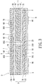
- the present invention provides a flexible thin image-sensing module D with anti-EMI (Anti Electromagnetic Interference) function, including: a flexible substrate unit 1, a first conductive unit 2, a protection unit 3, an anti-EMI unit 4, a second conductive layer 5, an electronic element unit 6, and a third conductive unit 7.
- EMI Anti Electromagnetic Interference
- the flexible substrate unit 1 has at least one through hole 100.
- the flexible substrate unit 1 can be a flexible copper foil clad laminate (FCCL).
- FCCL flexible copper foil clad laminate
- the flexible substrate unit 1 has a base film 11, a first base copper foil 12 disposed on a top surface of the base film 11 and a second base copper foil 13 disposed on a bottom surface of the base film 11, and the through hole 100 passes through the first base copper foil 12, the base film 11 and the second base copper foil 13.
- FCCL is just an example, and it does not limit the present invention. Any elastic substrate or flexible substrate can be applied in the present invention.
- the first conductive unit 2 has a first conductive layer 21 disposed on a bottom surface of the flexible substrate unit 1, a second conductive layer 22 disposed on a top surface of the flexible substrate unit 1, and a third conductive layer 23 disposed on an inner surface of the through hole 100 and electrically connected between the first conductive layer 21 and the second conductive layer 22.
- the first conductive unit 2 can be an electrodeposited copper foil.
- the third conductive layer 23 also can completely fill out the through hole 100 according to different requirements.
- the protection unit 3 has a first adhesive layer 31 disposed on the first conductive layer 21, a first covering layer 32 disposed on the first adhesive layer 31, a second adhesive layer 33 disposed on the second conductive layer 22, and a second covering layer 34 disposed on the second adhesive layer 33.
- the protection unit 3 has at least one first hole 301 passing through the first adhesive layer 31 and the first covering layer 32 and a plurality of second holes 302 passing through the second adhesive layer 33 and the second covering layer 34.
- the anti-EMI unit 4 is disposed on the first covering layer 32, and the anti-EMI unit 4 can be a grounding film for guiding electromagnetic waves generated by the electronic element unit 6 to the anti-EMI unit 4 in order to decrease the electromagnetic interference of the electronic element unit 6.
- the total thickness of the flexible substrate unit 1, the first conductive unit 2 and the anti-EMI unit 4 is between 0.1mm and 0.35mm. For example, 0.1mm ⁇ the total thickness ⁇ 0.35mm.
- the second conductive unit 5 has a first conductive body 50 filling out the first hole 301, and the first conductive body 50 is electrically connected between the first conductive layer 21 of the first conductive unit 2 and the anti-EMI unit 4.
- the electronic element unit 6 has a plurality of electronic elements 60 disposed on the second covering layer 34, and the electronic elements at least comprise an image sensor, a low dropout (LDO) regulator and a backend IC.
- the above-mentioned electronic elements are just examples, and these do not limit the present invention.
- the third conductive unit 7 has a plurality of second conductive bodies 70 respectively filling out the second holes 302, and the second conductive bodies 70 are electrically connected between the second conductive layer 22 of the first conductive unit 2 and the electronic element unit 6.
- the present invention further includes an adhesive unit 8 that has a plurality of adhesive films 80 disposed on the anti-EMI unit 4.
- Each adhesive film 80 can be a film with adhesive function and without conductive function.
- the flexible thin image-sensing module D can be positioned on any object via the adhesive films 80.
- the present invention provides a flexible thin image-sensing module D with anti-EMI function, including: a flexible substrate unit 1, an electronic element unit 6, an anti-EMI unit 4 and a conductive structure.
- the electronic element unit 6 has a plurality of electronic elements 60 disposed on a top surface of the flexible substrate unit 1, and the electronic elements 60 at least includes an image sensor, a low dropout regulator and a backend IC.
- the anti-EMI unit 4 is disposed on a bottom surface of the flexible substrate unit 1.
- the conductive structure is composed of a first conductive unit 2, a protection unit 3, a second conductive unit 5 and a third conductive unit 7, and the conductive structure passes through the flexible substrate unit 1 and is electrically connected between the electronic element unit 6 and the anti-EMI unit 4 in order to guide electromagnetic waves generated by the electronic element unit 6 to the anti-EMI unit 4.
- the present invention provides a flexible thin PCB module with anti-EMI function.
- the flexible thin PCB module can be applied to different fields according to the types of the electronic elements 60.
- the flexible thin PCB module includes a flexible substrate unit 1, an electronic element unit 6, an anti-EMI unit 4 and a conductive structure.
- the electronic element unit 6 has a plurality of electronic elements 60 disposed on a top surface of the flexible substrate unit 1.
- the anti-EMI unit 4 is disposed on a bottom surface of the flexible substrate unit 1.
- the conductive structure is composed of a first conductive unit 2, a protection unit 3, a second conductive unit 5 and a third conductive unit 7, and the conductive structure passes through the flexible substrate unit 1 and is electrically connected between the electronic element unit 6 and the anti-EMI unit 4 in order to guide electromagnetic waves generated by the electronic element unit 6 to the anti-EMI unit 4.
- the front side of the top cover C can be designed as an inclination shape due to the reduced thickness of the flexible thin image-sensing module D.
- the whole feeling thickness of the notebook N is reduced due to the inclination shape formed on the front side of the top cover C.
- the present invention has the following advantages:
Landscapes
- Physics & Mathematics (AREA)
- Electromagnetism (AREA)
- Engineering & Computer Science (AREA)
- Microelectronics & Electronic Packaging (AREA)
- Structure Of Printed Boards (AREA)
- Shielding Devices Or Components To Electric Or Magnetic Fields (AREA)
- Studio Devices (AREA)
Claims (3)
- Flexibles Bilderfassungsmodul (D) mit Anti-EMI-Funktion, aufweisend:eine flexible Substrateinheit (1), welche mindestens ein dadurch verlaufendes Durchgangsloch (100) aufweist,eine erste leitfähige Einheit (2), welche eine erste leitfähige Schicht (21), die an einer unteren Fläche der flexiblen Substrateinheit (1) angeordnet ist, eine zweite leitfähige Schicht (22), die an einer oberen Fläche der flexiblen Substrateinheit (1) angeordnet ist, und eine dritte leitfähige Schicht (23) hat, welche durch das Durchgangsloch (100) verläuft und elektrisch zwischen die erste leitfähige Schicht (21) und die zweite leitfähige Schicht (22) geschaltet ist,eine Schutzeinheit (3), welche eine erste Haftschicht (31), die an der ersten leitfähigen Schicht (21) angeordnet ist, eine erste Deckschicht (32), die an der ersten Haftschicht (31) angeordnet ist, eine zweite Haftschicht (33), die an der zweiten leitfähigen Schicht (22) angeordnet ist, und eine zweite Deckschicht (34) hat, die an der zweiten Haftschicht (33) angeordnet ist, wobei die Schutzeinheit (3) mindestens ein erstes Loch (301), welches durch die erste Haftschicht (31) und durch die erste Deckschicht (32) verläuft, und eine Mehrzahl von zweiten Löchern (302) hat, die durch die zweite Haftschicht (33) und durch die zweite Deckschicht (34) verlaufen,eine Anti-EMI-Einheit (4), welche an der ersten Deckschicht (32) angeordnet ist,eine zweite leitfähige Einheit (5), welche einen ersten leitfähigen Körper (50) hat, wobei das erste Loch (301) mit dem ersten leitfähigen Körper (50) gefüllt ist und der erste leitfähige Körper (50) zwei Enden hat, welche die erste leitfähige Schicht (21) beziehungsweise die Anti-EMI-Einheit (4) elektrisch kontaktieren,eine elektronisches-Bauteil-Einheit (6), welche eine Mehrzahl von elektronischen Bauteilen (60) hat, die an der zweiten Deckschicht (34) angeordnet sind, wobei eines der elektronischen Bauteile (60) ein Bildsensor ist und die elektronischen Bauteile (60) von dem flexiblen Bilderfassungsmodul (D) freiliegen, undeine dritte leitfähige Einheit (7), welche eine Mehrzahl von zweiten leitfähigen Körpern (70) hat,wobei die zweiten Löcher (302) jeweils mit den zweiten leitfähigen Körpern (70) gefüllt sind und jeder der zweiten leitfähigen Körper (70) zwei Enden hat, die die zweite leitfähige Schicht (22) beziehungsweise das entsprechende elektronische Bauteil (6) elektrisch kontaktieren,wobei die Anti-EMI-Einheit (4), die erste Deckschicht (32), die erste Haftschicht (31), die erste leitfähige Schicht (21), die flexible Substrateinheit (1), die zweite leitfähige Schicht (22), die zweite Haftschicht (33), die zweite Deckschicht (34) und die elektronisches-Bauteil-Einheit (6) übereinander angeordnet sind, wobei die Anti-EMI-Einheit (4) und die elektronisches-Bauteil-Einheit (6) an zwei gegenüberliegenden Seiten des flexiblen Bilderfassungsmoduls (D) angeordnet sind, die Anti-EMI-Einheit (4) eine unterste Einheit des flexiblen Bilderfassungsmoduls (D) ist und die elektronisches-Bauteil-Einheit (6) eine oberste Einheit des flexiblen Bilderfassungsmoduls (D) ist,wobei die elektronischen Bauteile (60) mit der Anti-EMI-Einheit (4) in Reihe elektrisch verbunden sind durch die zweiten leitfähigen Körper (70), die zweite leitfähige Schicht (22), die dritte leitfähige Schicht (23), die erste leitfähige Schicht (21) und den ersten leitfähigen Körper (50),wobei die Gesamtdicke der flexiblen Substrateinheit (1), der ersten leitfähigen Einheit (2) und der Anti-EMI-Einheit (4) zwischen 0,1 mm und 0,35 mm beträgt,wobei der Bildsensor (60) und die Anti-EMI-Einheit (4) jeweils zugeordnet an zwei gegenüberliegenden Flächen der Schutzeinheit (3) angeordnet sind,wobei der Bildsensor (60) und die Anti-EMI-Einheit (4) außerhalb der Schutzeinheit (3) und der flexiblen Substrateinheit (1) freiliegen,wobei der Bildsensor (60) und die Anti-EMI-Einheit (4) miteinander verbunden sind durch die zweiten leitfähigen Körper (70) innerhalb der Schutzeinheit (3), die erste leitfähige Einheit (2) innerhalb der flexiblen Substrateinheit (1) und dem ersten leitfähigen Körper (50) innerhalb der Schutzeinheit (3).
- Flexibles Bilderfassungsmodul (D) gemäß Anspruch 1, wobei die flexible Substrateinheit (1) eine mit flexibler Kupferfolie plattierte Laminierung ist und einen Basisfilm (11), eine erste Basiskupferfolie (12), die an einer oberen Fläche des Basisfilms (11) angeordnet ist, und eine zweite Basiskupferfolie hat, die an einer unteren Fläche des Basisfilms (11) angeordnet ist, und das Durchgangsloch (100) durch die erste Basiskupferfolie (12), den Basisfilm (11) und die zweite Basiskupferfolie hindurch verläuft.
- Flexibles Bilderfassungsmodul (D) gemäß Anspruch 1, wobei die erste leitfähige Einheit (2) eine galvanisch abgeschiedene Kupferfolie ist, die elektronischen Bauteile (60) zumindest einen Regler mit geringem Spannungsabfall und einen Backend-IC aufweisen, und die Anti-EMI-Einheit (4) ein Erdungsfilm ist.
Applications Claiming Priority (1)
| Application Number | Priority Date | Filing Date | Title |
|---|---|---|---|
| TW098111647A TWI372558B (en) | 2009-04-08 | 2009-04-08 | Flexible thin image-sensing module with anti-emi function and flexible thin pcb module with anti-emi function |
Publications (3)
| Publication Number | Publication Date |
|---|---|
| EP2239779A2 EP2239779A2 (de) | 2010-10-13 |
| EP2239779A3 EP2239779A3 (de) | 2012-09-26 |
| EP2239779B1 true EP2239779B1 (de) | 2017-05-24 |
Family
ID=41127907
Family Applications (1)
| Application Number | Title | Priority Date | Filing Date |
|---|---|---|---|
| EP09162940.2A Active EP2239779B1 (de) | 2009-04-08 | 2009-06-17 | Flexibles Bildsensormodul mit Anti-EMI-Funktion |
Country Status (3)
| Country | Link |
|---|---|
| US (1) | US8093509B2 (de) |
| EP (1) | EP2239779B1 (de) |
| TW (1) | TWI372558B (de) |
Families Citing this family (3)
| Publication number | Priority date | Publication date | Assignee | Title |
|---|---|---|---|---|
| US8670588B2 (en) * | 2009-09-08 | 2014-03-11 | Apple Inc. | Handheld device assembly |
| CN109949526B (zh) * | 2017-12-20 | 2023-11-03 | 上海箱箱物流科技有限公司 | 物流器具及其防拆卸方法 |
| KR102058865B1 (ko) * | 2018-04-12 | 2019-12-24 | (주)아이엠 | 초가속 열소재를 이용한 발열 디바이스 및 이의 제조방법 |
Citations (2)
| Publication number | Priority date | Publication date | Assignee | Title |
|---|---|---|---|---|
| US20040222352A1 (en) * | 2003-05-09 | 2004-11-11 | Matsushita Electric Industrial Co., Ltd. | Imaging apparatus |
| US20070119620A1 (en) * | 2005-11-29 | 2007-05-31 | Rodriguez Jose F | Flexible circuit shields |
Family Cites Families (13)
| Publication number | Priority date | Publication date | Assignee | Title |
|---|---|---|---|---|
| WO1994018815A1 (en) * | 1993-02-11 | 1994-08-18 | Telefonaktiebolaget Lm Ericsson | A flexible device for encapsulating electronic components |
| US5519585A (en) * | 1993-04-12 | 1996-05-21 | Dell Usa, L.P. | Sandwiched insulative/conductive layer EMI shield structure for printed circuit board |
| SE504195C2 (sv) * | 1995-03-21 | 1996-12-02 | Ericsson Telefon Ab L M | Laminat för förslutning och kapsling av elektroniska komponenter, samt sätt för dess framställning |
| US5917149A (en) * | 1997-05-15 | 1999-06-29 | Daimlerchrysler Corporation | Flexible circuit board interconnect with strain relief |
| GB2351183B (en) * | 1999-06-18 | 2003-10-15 | Nokia Mobile Phones Ltd | Shielding can for a printed circuit board |
| JP2001244583A (ja) * | 2000-02-29 | 2001-09-07 | Fuji Photo Optical Co Ltd | フレキシブル回路基板 |
| US6900383B2 (en) * | 2001-03-19 | 2005-05-31 | Hewlett-Packard Development Company, L.P. | Board-level EMI shield that adheres to and conforms with printed circuit board component and board surfaces |
| US20030214802A1 (en) * | 2001-06-15 | 2003-11-20 | Fjelstad Joseph C. | Signal transmission structure with an air dielectric |
| JP2005303067A (ja) * | 2004-04-13 | 2005-10-27 | Mitsubishi Electric Corp | 電子部品のシールド構造 |
| DE102005000655A1 (de) * | 2005-01-04 | 2006-07-13 | Robert Bosch Gmbh | Bilderfassungseinrichtung |
| WO2008053520A1 (en) * | 2006-10-30 | 2008-05-08 | Ibiden Co., Ltd. | Flex rigid wiring board and method for manufacturing the same |
| US7977582B2 (en) * | 2008-01-28 | 2011-07-12 | International Business Machines Corporation | Flexible multilayer printed circuit assembly with reduced EMI emissions |
| WO2009113202A1 (ja) * | 2008-03-10 | 2009-09-17 | イビデン株式会社 | フレキシブル配線板及びその製造方法 |
-
2009
- 2009-04-08 TW TW098111647A patent/TWI372558B/zh active
- 2009-06-09 US US12/457,347 patent/US8093509B2/en active Active
- 2009-06-17 EP EP09162940.2A patent/EP2239779B1/de active Active
Patent Citations (2)
| Publication number | Priority date | Publication date | Assignee | Title |
|---|---|---|---|---|
| US20040222352A1 (en) * | 2003-05-09 | 2004-11-11 | Matsushita Electric Industrial Co., Ltd. | Imaging apparatus |
| US20070119620A1 (en) * | 2005-11-29 | 2007-05-31 | Rodriguez Jose F | Flexible circuit shields |
Also Published As
| Publication number | Publication date |
|---|---|
| US8093509B2 (en) | 2012-01-10 |
| EP2239779A2 (de) | 2010-10-13 |
| TWI372558B (en) | 2012-09-11 |
| TW201038059A (en) | 2010-10-16 |
| EP2239779A3 (de) | 2012-09-26 |
| US20100258343A1 (en) | 2010-10-14 |
Similar Documents
| Publication | Publication Date | Title |
|---|---|---|
| US10860054B2 (en) | Electronic devices with cover layers mounted to displays | |
| US9098242B2 (en) | Electronic devices with cover layers mounted to displays | |
| US8054639B2 (en) | Image-sensing module for reducing overall thickness thereof and preventing EMI | |
| US7952889B2 (en) | Stacking structure of printed circuit board | |
| US20130162543A1 (en) | Piezoelectric Actuator Interface and Method | |
| US9345134B2 (en) | Printed wiring board | |
| US20140048310A1 (en) | Printed Circuit Solder Connections | |
| CN104904327A (zh) | 电子设备的窄边框显示器 | |
| US20090073672A1 (en) | Electromagnetic shield and electronic device using the same | |
| CN105960157A (zh) | 电磁屏蔽保护膜与fpc | |
| TW201408149A (zh) | 電路板組件及相機模組 | |
| CN110099509A (zh) | 电路板及电子设备 | |
| US7813138B2 (en) | Electronic device | |
| EP2239779B1 (de) | Flexibles Bildsensormodul mit Anti-EMI-Funktion | |
| US10854362B2 (en) | Guide-connected contactor and portable electronic device comprising same | |
| US20030220129A1 (en) | Mobile phone with dual PCB structure | |
| KR101053296B1 (ko) | 전자파 차폐 기능을 갖는 전자 장치 | |
| CN101277581A (zh) | 电路板的电磁防护方法及电路板组件 | |
| CN112449477B (zh) | 电路板的制造方法及电路板 | |
| CN101877347B (zh) | 具防电磁干扰的可挠性薄型图像感测模块及电路板模块 | |
| US8305765B2 (en) | Electronic apparatus | |
| CN101728367B (zh) | 用于降低整体厚度及防止电磁干扰的影像感测模块 | |
| JP2008078205A (ja) | 基板組立体及びその製造方法、電子部品組立体及びその製造方法、電子装置 | |
| CN119942915B (zh) | 显示模组及显示装置 | |
| US11439011B2 (en) | Electronic device module and method of manufacturing electronic device module |
Legal Events
| Date | Code | Title | Description |
|---|---|---|---|
| PUAI | Public reference made under article 153(3) epc to a published international application that has entered the european phase |
Free format text: ORIGINAL CODE: 0009012 |
|
| AK | Designated contracting states |
Kind code of ref document: A2 Designated state(s): AT BE BG CH CY CZ DE DK EE ES FI FR GB GR HR HU IE IS IT LI LT LU LV MC MK MT NL NO PL PT RO SE SI SK TR |
|
| AX | Request for extension of the european patent |
Extension state: AL BA RS |
|
| PUAL | Search report despatched |
Free format text: ORIGINAL CODE: 0009013 |
|
| AK | Designated contracting states |
Kind code of ref document: A3 Designated state(s): AT BE BG CH CY CZ DE DK EE ES FI FR GB GR HR HU IE IS IT LI LT LU LV MC MK MT NL NO PL PT RO SE SI SK TR |
|
| AX | Request for extension of the european patent |
Extension state: AL BA RS |
|
| RIC1 | Information provided on ipc code assigned before grant |
Ipc: H01L 27/146 20060101AFI20120817BHEP |
|
| 17P | Request for examination filed |
Effective date: 20130107 |
|
| 17Q | First examination report despatched |
Effective date: 20130627 |
|
| REG | Reference to a national code |
Ref country code: DE Ref legal event code: R079 Ref document number: 602009046237 Country of ref document: DE Free format text: PREVIOUS MAIN CLASS: H01L0027146000 Ipc: H05K0001180000 |
|
| GRAP | Despatch of communication of intention to grant a patent |
Free format text: ORIGINAL CODE: EPIDOSNIGR1 |
|
| INTG | Intention to grant announced |
Effective date: 20161215 |
|
| RIC1 | Information provided on ipc code assigned before grant |
Ipc: H05K 1/18 20060101AFI20161206BHEP Ipc: H01L 27/146 20060101ALI20161206BHEP Ipc: H05K 1/02 20060101ALI20161206BHEP |
|
| GRAS | Grant fee paid |
Free format text: ORIGINAL CODE: EPIDOSNIGR3 |
|
| GRAA | (expected) grant |
Free format text: ORIGINAL CODE: 0009210 |
|
| AK | Designated contracting states |
Kind code of ref document: B1 Designated state(s): AT BE BG CH CY CZ DE DK EE ES FI FR GB GR HR HU IE IS IT LI LT LU LV MC MK MT NL NO PL PT RO SE SI SK TR |
|
| REG | Reference to a national code |
Ref country code: GB Ref legal event code: FG4D |
|
| REG | Reference to a national code |
Ref country code: CH Ref legal event code: EP |
|
| REG | Reference to a national code |
Ref country code: IE Ref legal event code: FG4D |
|
| REG | Reference to a national code |
Ref country code: AT Ref legal event code: REF Ref document number: 896590 Country of ref document: AT Kind code of ref document: T Effective date: 20170615 |
|
| REG | Reference to a national code |
Ref country code: FR Ref legal event code: PLFP Year of fee payment: 9 |
|
| REG | Reference to a national code |
Ref country code: DE Ref legal event code: R096 Ref document number: 602009046237 Country of ref document: DE |
|
| REG | Reference to a national code |
Ref country code: NL Ref legal event code: MP Effective date: 20170524 |
|
| REG | Reference to a national code |
Ref country code: LT Ref legal event code: MG4D |
|
| REG | Reference to a national code |
Ref country code: AT Ref legal event code: MK05 Ref document number: 896590 Country of ref document: AT Kind code of ref document: T Effective date: 20170524 |
|
| PG25 | Lapsed in a contracting state [announced via postgrant information from national office to epo] |
Ref country code: AT Free format text: LAPSE BECAUSE OF FAILURE TO SUBMIT A TRANSLATION OF THE DESCRIPTION OR TO PAY THE FEE WITHIN THE PRESCRIBED TIME-LIMIT Effective date: 20170524 Ref country code: NO Free format text: LAPSE BECAUSE OF FAILURE TO SUBMIT A TRANSLATION OF THE DESCRIPTION OR TO PAY THE FEE WITHIN THE PRESCRIBED TIME-LIMIT Effective date: 20170824 Ref country code: HR Free format text: LAPSE BECAUSE OF FAILURE TO SUBMIT A TRANSLATION OF THE DESCRIPTION OR TO PAY THE FEE WITHIN THE PRESCRIBED TIME-LIMIT Effective date: 20170524 Ref country code: ES Free format text: LAPSE BECAUSE OF FAILURE TO SUBMIT A TRANSLATION OF THE DESCRIPTION OR TO PAY THE FEE WITHIN THE PRESCRIBED TIME-LIMIT Effective date: 20170524 Ref country code: LT Free format text: LAPSE BECAUSE OF FAILURE TO SUBMIT A TRANSLATION OF THE DESCRIPTION OR TO PAY THE FEE WITHIN THE PRESCRIBED TIME-LIMIT Effective date: 20170524 Ref country code: GR Free format text: LAPSE BECAUSE OF FAILURE TO SUBMIT A TRANSLATION OF THE DESCRIPTION OR TO PAY THE FEE WITHIN THE PRESCRIBED TIME-LIMIT Effective date: 20170825 Ref country code: FI Free format text: LAPSE BECAUSE OF FAILURE TO SUBMIT A TRANSLATION OF THE DESCRIPTION OR TO PAY THE FEE WITHIN THE PRESCRIBED TIME-LIMIT Effective date: 20170524 |
|
| PG25 | Lapsed in a contracting state [announced via postgrant information from national office to epo] |
Ref country code: NL Free format text: LAPSE BECAUSE OF FAILURE TO SUBMIT A TRANSLATION OF THE DESCRIPTION OR TO PAY THE FEE WITHIN THE PRESCRIBED TIME-LIMIT Effective date: 20170524 Ref country code: LV Free format text: LAPSE BECAUSE OF FAILURE TO SUBMIT A TRANSLATION OF THE DESCRIPTION OR TO PAY THE FEE WITHIN THE PRESCRIBED TIME-LIMIT Effective date: 20170524 Ref country code: IS Free format text: LAPSE BECAUSE OF FAILURE TO SUBMIT A TRANSLATION OF THE DESCRIPTION OR TO PAY THE FEE WITHIN THE PRESCRIBED TIME-LIMIT Effective date: 20170924 Ref country code: SE Free format text: LAPSE BECAUSE OF FAILURE TO SUBMIT A TRANSLATION OF THE DESCRIPTION OR TO PAY THE FEE WITHIN THE PRESCRIBED TIME-LIMIT Effective date: 20170524 Ref country code: BG Free format text: LAPSE BECAUSE OF FAILURE TO SUBMIT A TRANSLATION OF THE DESCRIPTION OR TO PAY THE FEE WITHIN THE PRESCRIBED TIME-LIMIT Effective date: 20170824 |
|
| PG25 | Lapsed in a contracting state [announced via postgrant information from national office to epo] |
Ref country code: CZ Free format text: LAPSE BECAUSE OF FAILURE TO SUBMIT A TRANSLATION OF THE DESCRIPTION OR TO PAY THE FEE WITHIN THE PRESCRIBED TIME-LIMIT Effective date: 20170524 Ref country code: DK Free format text: LAPSE BECAUSE OF FAILURE TO SUBMIT A TRANSLATION OF THE DESCRIPTION OR TO PAY THE FEE WITHIN THE PRESCRIBED TIME-LIMIT Effective date: 20170524 Ref country code: RO Free format text: LAPSE BECAUSE OF FAILURE TO SUBMIT A TRANSLATION OF THE DESCRIPTION OR TO PAY THE FEE WITHIN THE PRESCRIBED TIME-LIMIT Effective date: 20170524 Ref country code: EE Free format text: LAPSE BECAUSE OF FAILURE TO SUBMIT A TRANSLATION OF THE DESCRIPTION OR TO PAY THE FEE WITHIN THE PRESCRIBED TIME-LIMIT Effective date: 20170524 Ref country code: SK Free format text: LAPSE BECAUSE OF FAILURE TO SUBMIT A TRANSLATION OF THE DESCRIPTION OR TO PAY THE FEE WITHIN THE PRESCRIBED TIME-LIMIT Effective date: 20170524 |
|
| REG | Reference to a national code |
Ref country code: CH Ref legal event code: PL |
|
| REG | Reference to a national code |
Ref country code: DE Ref legal event code: R097 Ref document number: 602009046237 Country of ref document: DE |
|
| PG25 | Lapsed in a contracting state [announced via postgrant information from national office to epo] |
Ref country code: IT Free format text: LAPSE BECAUSE OF FAILURE TO SUBMIT A TRANSLATION OF THE DESCRIPTION OR TO PAY THE FEE WITHIN THE PRESCRIBED TIME-LIMIT Effective date: 20170524 Ref country code: PL Free format text: LAPSE BECAUSE OF FAILURE TO SUBMIT A TRANSLATION OF THE DESCRIPTION OR TO PAY THE FEE WITHIN THE PRESCRIBED TIME-LIMIT Effective date: 20170524 |
|
| REG | Reference to a national code |
Ref country code: IE Ref legal event code: MM4A |
|
| PLBE | No opposition filed within time limit |
Free format text: ORIGINAL CODE: 0009261 |
|
| STAA | Information on the status of an ep patent application or granted ep patent |
Free format text: STATUS: NO OPPOSITION FILED WITHIN TIME LIMIT |
|
| PG25 | Lapsed in a contracting state [announced via postgrant information from national office to epo] |
Ref country code: IE Free format text: LAPSE BECAUSE OF NON-PAYMENT OF DUE FEES Effective date: 20170617 Ref country code: LU Free format text: LAPSE BECAUSE OF NON-PAYMENT OF DUE FEES Effective date: 20170617 Ref country code: LI Free format text: LAPSE BECAUSE OF NON-PAYMENT OF DUE FEES Effective date: 20170630 Ref country code: CH Free format text: LAPSE BECAUSE OF NON-PAYMENT OF DUE FEES Effective date: 20170630 |
|
| 26N | No opposition filed |
Effective date: 20180227 |
|
| REG | Reference to a national code |
Ref country code: BE Ref legal event code: MM Effective date: 20170630 |
|
| PG25 | Lapsed in a contracting state [announced via postgrant information from national office to epo] |
Ref country code: SI Free format text: LAPSE BECAUSE OF FAILURE TO SUBMIT A TRANSLATION OF THE DESCRIPTION OR TO PAY THE FEE WITHIN THE PRESCRIBED TIME-LIMIT Effective date: 20170524 |
|
| REG | Reference to a national code |
Ref country code: FR Ref legal event code: PLFP Year of fee payment: 10 |
|
| PG25 | Lapsed in a contracting state [announced via postgrant information from national office to epo] |
Ref country code: BE Free format text: LAPSE BECAUSE OF NON-PAYMENT OF DUE FEES Effective date: 20170630 |
|
| PG25 | Lapsed in a contracting state [announced via postgrant information from national office to epo] |
Ref country code: MT Free format text: LAPSE BECAUSE OF NON-PAYMENT OF DUE FEES Effective date: 20170617 |
|
| PG25 | Lapsed in a contracting state [announced via postgrant information from national office to epo] |
Ref country code: HU Free format text: LAPSE BECAUSE OF FAILURE TO SUBMIT A TRANSLATION OF THE DESCRIPTION OR TO PAY THE FEE WITHIN THE PRESCRIBED TIME-LIMIT; INVALID AB INITIO Effective date: 20090617 Ref country code: MC Free format text: LAPSE BECAUSE OF FAILURE TO SUBMIT A TRANSLATION OF THE DESCRIPTION OR TO PAY THE FEE WITHIN THE PRESCRIBED TIME-LIMIT Effective date: 20170524 |
|
| PG25 | Lapsed in a contracting state [announced via postgrant information from national office to epo] |
Ref country code: CY Free format text: LAPSE BECAUSE OF NON-PAYMENT OF DUE FEES Effective date: 20170524 |
|
| PG25 | Lapsed in a contracting state [announced via postgrant information from national office to epo] |
Ref country code: MK Free format text: LAPSE BECAUSE OF FAILURE TO SUBMIT A TRANSLATION OF THE DESCRIPTION OR TO PAY THE FEE WITHIN THE PRESCRIBED TIME-LIMIT Effective date: 20170524 |
|
| PG25 | Lapsed in a contracting state [announced via postgrant information from national office to epo] |
Ref country code: TR Free format text: LAPSE BECAUSE OF FAILURE TO SUBMIT A TRANSLATION OF THE DESCRIPTION OR TO PAY THE FEE WITHIN THE PRESCRIBED TIME-LIMIT Effective date: 20170524 |
|
| PG25 | Lapsed in a contracting state [announced via postgrant information from national office to epo] |
Ref country code: PT Free format text: LAPSE BECAUSE OF FAILURE TO SUBMIT A TRANSLATION OF THE DESCRIPTION OR TO PAY THE FEE WITHIN THE PRESCRIBED TIME-LIMIT Effective date: 20170524 |
|
| PGFP | Annual fee paid to national office [announced via postgrant information from national office to epo] |
Ref country code: DE Payment date: 20250514 Year of fee payment: 17 |
|
| PGFP | Annual fee paid to national office [announced via postgrant information from national office to epo] |
Ref country code: GB Payment date: 20250508 Year of fee payment: 17 |
|
| PGFP | Annual fee paid to national office [announced via postgrant information from national office to epo] |
Ref country code: FR Payment date: 20250508 Year of fee payment: 17 |