EP2234805B1 - Optical film laminates - Google Patents
Optical film laminates Download PDFInfo
- Publication number
- EP2234805B1 EP2234805B1 EP08859092A EP08859092A EP2234805B1 EP 2234805 B1 EP2234805 B1 EP 2234805B1 EP 08859092 A EP08859092 A EP 08859092A EP 08859092 A EP08859092 A EP 08859092A EP 2234805 B1 EP2234805 B1 EP 2234805B1
- Authority
- EP
- European Patent Office
- Prior art keywords
- film
- pet
- optical film
- films
- film laminate
- Prior art date
- Legal status (The legal status is an assumption and is not a legal conclusion. Google has not performed a legal analysis and makes no representation as to the accuracy of the status listed.)
- Not-in-force
Links
Images
Classifications
-
- B—PERFORMING OPERATIONS; TRANSPORTING
- B32—LAYERED PRODUCTS
- B32B—LAYERED PRODUCTS, i.e. PRODUCTS BUILT-UP OF STRATA OF FLAT OR NON-FLAT, e.g. CELLULAR OR HONEYCOMB, FORM
- B32B7/00—Layered products characterised by the relation between layers; Layered products characterised by the relative orientation of features between layers, or by the relative values of a measurable parameter between layers, i.e. products comprising layers having different physical, chemical or physicochemical properties; Layered products characterised by the interconnection of layers
- B32B7/04—Interconnection of layers
- B32B7/12—Interconnection of layers using interposed adhesives or interposed materials with bonding properties
-
- B—PERFORMING OPERATIONS; TRANSPORTING
- B32—LAYERED PRODUCTS
- B32B—LAYERED PRODUCTS, i.e. PRODUCTS BUILT-UP OF STRATA OF FLAT OR NON-FLAT, e.g. CELLULAR OR HONEYCOMB, FORM
- B32B27/00—Layered products comprising a layer of synthetic resin
- B32B27/06—Layered products comprising a layer of synthetic resin as the main or only constituent of a layer, which is next to another layer of the same or of a different material
- B32B27/08—Layered products comprising a layer of synthetic resin as the main or only constituent of a layer, which is next to another layer of the same or of a different material of synthetic resin
-
- B—PERFORMING OPERATIONS; TRANSPORTING
- B32—LAYERED PRODUCTS
- B32B—LAYERED PRODUCTS, i.e. PRODUCTS BUILT-UP OF STRATA OF FLAT OR NON-FLAT, e.g. CELLULAR OR HONEYCOMB, FORM
- B32B27/00—Layered products comprising a layer of synthetic resin
- B32B27/36—Layered products comprising a layer of synthetic resin comprising polyesters
-
- B—PERFORMING OPERATIONS; TRANSPORTING
- B32—LAYERED PRODUCTS
- B32B—LAYERED PRODUCTS, i.e. PRODUCTS BUILT-UP OF STRATA OF FLAT OR NON-FLAT, e.g. CELLULAR OR HONEYCOMB, FORM
- B32B3/00—Layered products comprising a layer with external or internal discontinuities or unevennesses, or a layer of non-planar shape; Layered products comprising a layer having particular features of form
- B32B3/26—Layered products comprising a layer with external or internal discontinuities or unevennesses, or a layer of non-planar shape; Layered products comprising a layer having particular features of form characterised by a particular shape of the outline of the cross-section of a continuous layer; characterised by a layer with cavities or internal voids ; characterised by an apertured layer
- B32B3/30—Layered products comprising a layer with external or internal discontinuities or unevennesses, or a layer of non-planar shape; Layered products comprising a layer having particular features of form characterised by a particular shape of the outline of the cross-section of a continuous layer; characterised by a layer with cavities or internal voids ; characterised by an apertured layer characterised by a layer formed with recesses or projections, e.g. hollows, grooves, protuberances, ribs
-
- G—PHYSICS
- G02—OPTICS
- G02B—OPTICAL ELEMENTS, SYSTEMS OR APPARATUS
- G02B5/00—Optical elements other than lenses
- G02B5/04—Prisms
- G02B5/045—Prism arrays
-
- B—PERFORMING OPERATIONS; TRANSPORTING
- B32—LAYERED PRODUCTS
- B32B—LAYERED PRODUCTS, i.e. PRODUCTS BUILT-UP OF STRATA OF FLAT OR NON-FLAT, e.g. CELLULAR OR HONEYCOMB, FORM
- B32B2250/00—Layers arrangement
- B32B2250/24—All layers being polymeric
- B32B2250/244—All polymers belonging to those covered by group B32B27/36
-
- B—PERFORMING OPERATIONS; TRANSPORTING
- B32—LAYERED PRODUCTS
- B32B—LAYERED PRODUCTS, i.e. PRODUCTS BUILT-UP OF STRATA OF FLAT OR NON-FLAT, e.g. CELLULAR OR HONEYCOMB, FORM
- B32B2255/00—Coating on the layer surface
- B32B2255/10—Coating on the layer surface on synthetic resin layer or on natural or synthetic rubber layer
-
- B—PERFORMING OPERATIONS; TRANSPORTING
- B32—LAYERED PRODUCTS
- B32B—LAYERED PRODUCTS, i.e. PRODUCTS BUILT-UP OF STRATA OF FLAT OR NON-FLAT, e.g. CELLULAR OR HONEYCOMB, FORM
- B32B2255/00—Coating on the layer surface
- B32B2255/26—Polymeric coating
-
- B—PERFORMING OPERATIONS; TRANSPORTING
- B32—LAYERED PRODUCTS
- B32B—LAYERED PRODUCTS, i.e. PRODUCTS BUILT-UP OF STRATA OF FLAT OR NON-FLAT, e.g. CELLULAR OR HONEYCOMB, FORM
- B32B2270/00—Resin or rubber layer containing a blend of at least two different polymers
-
- B—PERFORMING OPERATIONS; TRANSPORTING
- B32—LAYERED PRODUCTS
- B32B—LAYERED PRODUCTS, i.e. PRODUCTS BUILT-UP OF STRATA OF FLAT OR NON-FLAT, e.g. CELLULAR OR HONEYCOMB, FORM
- B32B2307/00—Properties of the layers or laminate
- B32B2307/40—Properties of the layers or laminate having particular optical properties
- B32B2307/412—Transparent
-
- B—PERFORMING OPERATIONS; TRANSPORTING
- B32—LAYERED PRODUCTS
- B32B—LAYERED PRODUCTS, i.e. PRODUCTS BUILT-UP OF STRATA OF FLAT OR NON-FLAT, e.g. CELLULAR OR HONEYCOMB, FORM
- B32B2307/00—Properties of the layers or laminate
- B32B2307/40—Properties of the layers or laminate having particular optical properties
- B32B2307/42—Polarizing, birefringent, filtering
-
- B—PERFORMING OPERATIONS; TRANSPORTING
- B32—LAYERED PRODUCTS
- B32B—LAYERED PRODUCTS, i.e. PRODUCTS BUILT-UP OF STRATA OF FLAT OR NON-FLAT, e.g. CELLULAR OR HONEYCOMB, FORM
- B32B2307/00—Properties of the layers or laminate
- B32B2307/50—Properties of the layers or laminate having particular mechanical properties
- B32B2307/514—Oriented
- B32B2307/516—Oriented mono-axially
-
- B—PERFORMING OPERATIONS; TRANSPORTING
- B32—LAYERED PRODUCTS
- B32B—LAYERED PRODUCTS, i.e. PRODUCTS BUILT-UP OF STRATA OF FLAT OR NON-FLAT, e.g. CELLULAR OR HONEYCOMB, FORM
- B32B2307/00—Properties of the layers or laminate
- B32B2307/50—Properties of the layers or laminate having particular mechanical properties
- B32B2307/514—Oriented
- B32B2307/518—Oriented bi-axially
-
- B—PERFORMING OPERATIONS; TRANSPORTING
- B32—LAYERED PRODUCTS
- B32B—LAYERED PRODUCTS, i.e. PRODUCTS BUILT-UP OF STRATA OF FLAT OR NON-FLAT, e.g. CELLULAR OR HONEYCOMB, FORM
- B32B2307/00—Properties of the layers or laminate
- B32B2307/50—Properties of the layers or laminate having particular mechanical properties
- B32B2307/546—Flexural strength; Flexion stiffness
-
- B—PERFORMING OPERATIONS; TRANSPORTING
- B32—LAYERED PRODUCTS
- B32B—LAYERED PRODUCTS, i.e. PRODUCTS BUILT-UP OF STRATA OF FLAT OR NON-FLAT, e.g. CELLULAR OR HONEYCOMB, FORM
- B32B2307/00—Properties of the layers or laminate
- B32B2307/70—Other properties
- B32B2307/71—Resistive to light or to UV
-
- B—PERFORMING OPERATIONS; TRANSPORTING
- B32—LAYERED PRODUCTS
- B32B—LAYERED PRODUCTS, i.e. PRODUCTS BUILT-UP OF STRATA OF FLAT OR NON-FLAT, e.g. CELLULAR OR HONEYCOMB, FORM
- B32B2457/00—Electrical equipment
- B32B2457/20—Displays, e.g. liquid crystal displays, plasma displays
-
- B—PERFORMING OPERATIONS; TRANSPORTING
- B32—LAYERED PRODUCTS
- B32B—LAYERED PRODUCTS, i.e. PRODUCTS BUILT-UP OF STRATA OF FLAT OR NON-FLAT, e.g. CELLULAR OR HONEYCOMB, FORM
- B32B2457/00—Electrical equipment
- B32B2457/20—Displays, e.g. liquid crystal displays, plasma displays
- B32B2457/202—LCD, i.e. liquid crystal displays
-
- C—CHEMISTRY; METALLURGY
- C09—DYES; PAINTS; POLISHES; NATURAL RESINS; ADHESIVES; COMPOSITIONS NOT OTHERWISE PROVIDED FOR; APPLICATIONS OF MATERIALS NOT OTHERWISE PROVIDED FOR
- C09K—MATERIALS FOR MISCELLANEOUS APPLICATIONS, NOT PROVIDED FOR ELSEWHERE
- C09K2323/00—Functional layers of liquid crystal optical display excluding electroactive liquid crystal layer characterised by chemical composition
- C09K2323/06—Substrate layer characterised by chemical composition
-
- G—PHYSICS
- G02—OPTICS
- G02F—OPTICAL DEVICES OR ARRANGEMENTS FOR THE CONTROL OF LIGHT BY MODIFICATION OF THE OPTICAL PROPERTIES OF THE MEDIA OF THE ELEMENTS INVOLVED THEREIN; NON-LINEAR OPTICS; FREQUENCY-CHANGING OF LIGHT; OPTICAL LOGIC ELEMENTS; OPTICAL ANALOGUE/DIGITAL CONVERTERS
- G02F1/00—Devices or arrangements for the control of the intensity, colour, phase, polarisation or direction of light arriving from an independent light source, e.g. switching, gating or modulating; Non-linear optics
- G02F1/01—Devices or arrangements for the control of the intensity, colour, phase, polarisation or direction of light arriving from an independent light source, e.g. switching, gating or modulating; Non-linear optics for the control of the intensity, phase, polarisation or colour
- G02F1/13—Devices or arrangements for the control of the intensity, colour, phase, polarisation or direction of light arriving from an independent light source, e.g. switching, gating or modulating; Non-linear optics for the control of the intensity, phase, polarisation or colour based on liquid crystals, e.g. single liquid crystal display cells
- G02F1/133—Constructional arrangements; Operation of liquid crystal cells; Circuit arrangements
- G02F1/1333—Constructional arrangements; Manufacturing methods
- G02F1/1335—Structural association of cells with optical devices, e.g. polarisers or reflectors
- G02F1/13363—Birefringent elements, e.g. for optical compensation
Definitions
- the present invention relates to optical film laminates.
- the current invention provides a laminated brightness enhancement article that is self-supporting and resists waviness formation when used in a large LCD display.
- the invention also provides optical displays which comprise a light source, an LCD panel, and an optical film laminate of the invention between the light source and the LCD panel.
- “Structured surface” means a surface that has at least one geometric feature thereon and that has been created by any technique that imparts a desired geometric feature or plurality of geometric features to a surface.
- Such geometric structures have a pitch of from 30 to 300 micrometers. Examples of such geometric features include regular elongated prisms, random elongated prisms, discrete prisms, or beaded structures.
- Such structures can be applied by either cast and cure methods or by melt extrusion replication methods.
- Uniaxially oriented means a film that is oriented only in one in-plane direction through stretching of the film in that in-plane direction. Typical draw ratios range from 1.2 to 10;
- Biaxially oriented means is defined as stretching a film that is oriented in both in-plane directions through stretching the film in both directions. Typical draw ratios range from 1.2 to 8;
- Birefringence arises when the electron density distribution is no longer random in materials, causing the light travels at different speed at different directions.
- birefringence can be obtained by either uniaxially or biaxial stretching the film.
- machine direction MD
- TD transverse direction
- TM transmagnetic direction
- MD and TD are often referred as in-plane directions whereas TM is referred as out-of-plane direction.
- the in-plane birefringence, ⁇ n in is defined as the refractive index difference between the in-plane stretching direction and the in-plane un-stretched direction.
- ⁇ ⁇ n in n TD - n MD
- n MD , n TD , n TM are refractive index of the film in three directions.
- the film possesses positive in-plane birefringence and the material is positively birefringent. If ⁇ n in ⁇ 0, the film possesses negative in-plane birefringence and the material is negatively birefringent. Likewise, if ⁇ n out >0, the film possesses positive out-of-plane birefringence and the material is positively birefringent. If ⁇ n out ⁇ 0, the film possesses negative out-of-plane birefringence and the material is negatively birefringent.
- both in-plane and out-of-plane birefringence are positive for positively birefringent polymers, or polymers with substantially positive stress-optical coefficient.
- a constrained uniaxially stretched PET in TD direction by a draw ratio of 1x4 (MDxTD) will result in typical refractive index of 1.54, 1.66, 1.51 for MD, TD and TM, respectively.
- the in-plane birefringence is 0.12 whereas out-of-plane birefringence is 0.09, according to the equations (1) and (2), indicating PET is a positively birefringent polymer.
- both in-plane and out-of-plane birefringence can be substantially close to zero for non-birefringent polymers, or polymers with essentially zero stress-optical coefficient.
- stretching of polycarbonate will typically result in birefringence less than 0.005 in both in-plane and out-of-plane directions, indicating PC is not a strongly birefringent polymer.
- in-plane birefringence can be substantially zero when the film is stretched equally in both in-plane directions.
- the out-of-plane birefringence can be substantially positive due to the positive birefringent nature of the material.
- the polymer is substantially birefringent.
- a biaxially stretched PET film will draw ratios of 3.5 in both MD and TD has typical refractive index of 1.65, 1.65, and 1.50 for MD, TD and TM, respectively.
- the in-plane birefringence is 0.0 whereas out-of-plane birefringence is 0.15, according to the equations (1) and (2).
- the 0.15 out-of plane birefringence is substantially larger than zero, indicating PET is a positively birefringent polymer.
- the out-of-plane birefringence of the laminates of the invention is higher than 0.
- the out-of-plane birefringence of the laminates of the invention is higher than 0.05, higher than 0.10, or 0.15 or higher.
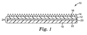
- optical film laminate 10 is comprised of a first polyester base film 12 having a structured surface 14 deposited on a first surface 16 of the first polyester base film.
- Second base film 18 is bonded to the second surface 20 of the first base film by means of an adhesive layer 22.
- the thickness 24 of the bonded first and second polyester base films is 10 mils (0.25 mm) or greater. In other embodiments, the thickness of the bonded first and second polyester base films is 11 mils (0.28 mm) or greater, 12 mils (0.30 mm) or greater, 13 mils (0.33 mm) or greater, or 14 mils (0.36 mm) or greater.
- the thickness of the bonded first and second polyester base films is 10 to 40 mils (0.25 to 1.0 mm), 10 to 35 mils (0.25 to 0.89 mm), 10 to 30 mils (0.25 to 0.76 mm), or 10 to 25 mils (0.25 to 0.64 mm).
- the polyester base films are birefringent. In certain embodiments the polyester base films are uniaxially oriented and in other embodiments, the polyester base films are biaxially oriented.
- the base films of the laminates of the invention have substantially the same shrinkage in the machine direction, the transverse direction, or in both directions, according to the procedure presented below.
- the films can be heat treated under the same conditions.
- polyester films can be exposed to temperatures of from 70 to 220 °C for a time ranging from 5 to 60 seconds.
- the polyester base films have a shrinkage difference of less than 1% in both the machine and transverse directions. In other embodiments, the polyester base films have a shrinkage difference of less than 0.5% in both the machine and transverse directions.
- each of the first and second polyester base films range from 5 mils (0.18 mm) to 15 mils (0.38 mm).
- the thickness of the adhesive layer between the first and second base layers ranges from 0.005 mil (0.13 micrometers) to 5 mils (0.18 mm).
- Useful polyester polymers used for making the first and second base films are polymers that are substantially transparent and having high stiffness, such materials include polyethylene terephthalate (PET), polyethylene naphthalate (PEN), polybutylene terephthalate (PBT), poly(ether esters), PET modified by at least one diacid, PET modified by at least one diol, PET modified by at least one diol and one diacid, PEN modified by at least one diacid, PEN modified by at least one diol, PEN modified by at least one diacid and one diol, and copolymers or blends of any of them.
- PET polyethylene terephthalate
- PEN polyethylene naphthalate
- PBT polybutylene terephthalate
- PET modified by at least one diacid PET modified by at least one diol
- PET modified by at least one diol and one diacid PET modified by at least one diol and one diacid
- PEN modified by at least one diacid PET modified
- the useful diol monomers include those having more than two hydroxyl groups, for example, triols, tetraols, and pentaols, may also be useful.
- aliphatic diols and glycols are useful; examples include 1,6-hexanediol; 1,4-butanediol; trimethylolpropane; 1,4-cyclohexanedimethanol; 1,4-benzenedimethanol; neopentyl glycol; ethylene glycol; propylene glycol; polyethylene glycol; tricyclodecanediol; norbomane diol; bicyclo-octanediol; pentaerythritol; bisphenol A; and 1,3-bis(2-hydroxyethoxy)benzene.
- the useful diacid monomers may comprise any dicarboxylate monomers known for preparing polyesters used in optical applications.
- dicarboxylate and “acid” are used interchangeably and include lower alkyl esters having from 1 to 10 carbon atoms.
- first dicarboxylate monomers include naphthalene dicarboxylic acid; terephthalate dicarboxylic acid; phthalate dicarboxylic acid; isophthalate dicarboxylic acid; (meth)acrylic acid; maleic acid; itaconic acid; azelaic acid; adipic acid; sebacic acid; norbornene dicarboxylic acid; bi-cyclooctane dicarboxylic acid; 1,6-cyclohexane dicarboxylic acid; t-butyl isophthalic acid; tri-mellitic acid; or combinations thereof; and which may be substituted by its dimethyl ester form.
- Useful adhesive materials for use in the adhesive layers are those that are optically clear and provide substantial adhesion at the interface of the optical films.
- Useful optically clear adhesives include those selected from UV curable acrylate adhesives, heat sealing adhesives, pressure sensitive adhesives, heat curable adhesives, dry-laminate adhesives, sulfonated polyester adhesives, and ultra-thin adhesives.
- the adhesive may also contain UV absorbing agents to deter degradation and anti-static particles to aid in film handling.
- adhesive materials having glass transition temperatures (T g ) of 0 °C or greater in their final application form are desirable. In other embodiments, the adhesive materials have a Tg of 10 °C or greater.
- the optical film laminates of the invention are made by laminating two birefringent polyester base films together using an adhesive layer.
- one of the polyester base films would have a structured surface formed or deposited on one surface before being bonded or laminated to the other polyester base film.
- the surfaces of the films in contact with the adhesive are first treated with an adhesion promoter such as a primer or physical surface treatments such as plasma, corona, e-beam, or flash-lamp treatments.
- the primers may further contain anti-static particles.
- the structured surface is formed by depositing or casting a resin onto a surface of a polyester film, forming the resin into structures, and then curing the resin, the surface of the base polyester film in contact with the resin is also typically treated first with an adhesion promoter.
- the structured surface may be disposed on a surface of the first base film by microembossing, incorporating a bulk diffusing material, such as beads into the film, by casting a resin, such as an acrylate resin, onto the surface and curing the resin.
- optical film laminates of the invention are useful in displays and particularly, those displays having a diagonal of greater than 37 in (94 cm), in other embodiments, 40 in (102 cm) or greater, 42 in (107 cm) or greater, 50 in (127 cm) or greater, 60 in (152 cm) or greater, 70 in (178 cm) or greater, or 100 in (254 cm) or greater.
- the diagonal can range from greater than 37 to 70 in (94 - 178 cm).
- the invention provides optical displays that comprise a light source, (for example, backlight or lightguide), an LCD panel, and an optical film laminate of the invention between the light source and the light gating device.
- a light source for example, backlight or lightguide
- an LCD panel for example, a liquid crystal display
- an optical film laminate of the invention between the light source and the light gating device.
- the structured surface of the optical film laminate would be facing up, or towards the LCD panel.
- the optical film may be adjacent to the light source or attached, or bonded to the light source.
- the stiffness of films and laminates were determined on an INSTRON 3342 equipped with a 50N load cell and a 3-point bending fixture. Samples were 25 mm wide. The crosshead speed was 0.5mm/min. Force was applied to the sample via the traveling crosshead, and the sample was contacted with an anvil having a 10 mm diameter. The two lower support anvils had a diameter of 3.94 mm each, and the center-to-center distance of these support anvils was 8.81 mm. Reported values in N/mm are based on the change in force N divided by the crosshead travel distance in mm for given change in force.
- the film haze was tested using a Hazeguard® instrument from BYK-Gamer USA. Haze was measured according to ASTM D-1003.
- Gain of the laminated articles was measured on an illumination box, referred as a gain cube that was used as the light source.
- the gain cube comprised a highly reflective cavity, with the light passing out of a Teflon ® surface to illuminate the samples. Baseline measurements were performed on top of the gain cube and then samples were placed on top of the gain cube and a measurement was taken. The gain was calculated by the luminance measured with a sample divided by the luminance measured without a sample on the gain cube.
- the measurements brightness and uniformity were performed on an LCD-TV (37 in (94 cm) diagonal) with a backlight configuration of cover sheet/sample/diffuser sheet.
- a spectrometer calibrated with a human eye's response was used for measuring bright luminance.
- Bright luminance and dark luminance was measured at 13 evenly distributed points over the display area. The average bright luminance was calculated.
- Contrast was calculated as the ratio of bright to dark luminance.
- Uniformity was calculated as the ratio of lowest to highest luminance when the TV was turned on.
- Brightness, contrast, and uniformity of each sample were compared against that of a monolithic PET film having a thickness of 10 mil (0.25 mm).
- a value of 100% means the sample has a performance equivalent to that of the base film.
- a value higher than 100% (>2%) means the sample has better performance than the base film.
- a value lower than 100% (>2%) means the sample tested has less performance than the base film.
- Warp performance of samples was evaluated using the Temperature Gradient Test, which is a system capable of testing warp in a 37in (94 cm) diagonal TV part in a controlled temperature gradient.
- the testing system consisted of an oven with a thermal bed capable of generating a precisely controlled temperature gradient.
- Each sample was tested with a thermal difference of 55, 50, 45, 35, and 30 °C across the sample to simulate thermal conditions in an actual LCD display.
- the system was programmed to cyclic heating (to the target gradient) and cooling (back to 23 °C throughout the part).
- the film surface topology was scanned during the cooling cycle to detect any wavy distortions, that is, warp. If warp was visually observed in the sample, the sample was marked as NG (not good). If warp was not visually observed, the sample was marked as G (good).
- Warp resistance was tested using a 47in (119 cm) LCD TV. Samples were cut, placed into the TV, and the TV was placed into an environmental chamber set at 60 °C and 90% relative humidity for 250 hours. The testing configuration was cover sheet/sample /diffuser sheet. After testing, the samples were taken out of the display and visually inspected for wavy distortions, that is warp. If warp was visually observed in the sample, the sample was marked as NG (not good). If warp was not visually observed, the sample was marked as G (good).
- Shrinkage was tested in both MD and TD.
- a convection oven capable of maintaining a target temperature within 2 °C was used with a set temperature of 150 °C.
- Sample strips of 2.54cm wide and 30 cm long were used.
- Two marks of 25.4 cm apart are drawn on the film to define the initial length ( L 0 ).
- Samples were hung in the oven for 15 minutes.
- the final length between to the two marks is measured ( L t ) .
- the refractive indices of the various samples were measured using a Metricon Prism coupler (Metricon Corporation, Pennington, N.J.) in the MD, TD, and TM directions. MD and TD are in-plane directions and TM is the sample normal. Glossary: UVA 1962 UV curable acrylic adhesive, commercially available from Toagosei Co. Ltd., JP. Tg ⁇ 25 °C UVA4856 UV curable acrylic adhesive, commercially available from Toagosei Co. Ltd., JP. Tg ⁇ 25 °C OCA Optically clear adhesive, #8141, available from 3M Company, St.
- Comparative example 1 A transparent PET film of 10 mil (0.25 mm) thickness was coated with WB54 on one side. An acrylic resin was then coated onto the surface using a roll-to-roll process. A mold was used to impart a structure. The structure was fixed by curing the acrylic resin under a UV lamp. The film showed some warp when tested according to the Module Warp Test and some warp when tested according to the Temperature Gradient Test. Comparative examples 2-3 were transparent PET films of 5 (0.13 mm) and 7 mil (0.18 mm) thickness. The films were not self-supportive (sagging) when sized to a 37in (94 cm) diagonal and above. The films showed significant warp when tested according to the Temperature Gradient Test and showed significant warp when tested according to the Module Warp Test.
- Comparative example 4 was a transparent PET film of 10 mil (0.25 mm) thickness. The film showed some warp when tested according to the Temperature Gradient Test and showed some warp when tested according to the Module Warp Test.
- Comparative example 5 was a single layer polyethylene terephthalate cast web was made on a pilot melt extrusion line using a polyethylene terephthalate resin made as follows: A batch reactor was charged with 158.9 kg dimethyl terephthalate (DMT), 0.2 kg of trimethylol propane (TMP), 108.1 kg ethylene glycol (EG), 32 g zinc(II) acetate, 32 g cobalt(II) acetate, and 80 g antimony(III) acetate. Under pressure of 239.2 kPa, this mixture was heated to 257 °C to remove esterification reaction by-product, methanol.
- DMT dimethyl terephthalate
- TMP trimethylol propane
- EG ethylene glycol
- EG ethylene glycol
- zinc(II) acetate 32 g zinc(II) acetate
- 32 g cobalt(II) acetate 32 g cobalt(II) acetate
- the cast web thickness was controlled by the casting speed such that the cast web was about 3.3 mm (130 mils). Such thickness would be necessary to form a 12 mil (0.30 mm) thick film after biaxial orientation.
- the cast web appeared cloudy and its haze was measured to be about 20%. Due to the high haze, it was believed that a 12 mil (0.30 mm) thick, highly transparent, and biaxially oriented PET film could not be made using the 3.3 mm thick cast web.
- Comparative example 6 was a single-layer cast polyethylene terephthalate web made in the same manner as in Comparative example 5, except the thickness of the cast web was at about 3.7 mm (148mils). Such thickness would be necessary to form a 14 mil (0.36 mm) thick film after biaxial orientation.
- the cast web appeared to be very cloudy and its haze was measured to be about 35%. Due to the high haze, it was believed that a 14mil-thick (0.36 mm), highly transparent, biaxially oriented PET film could not be made using the thick cast web.
- Comparative examples 7-8 Transparent PET films of 5 (0.13 mm) and 7mil (0.18 mm) thickness were hand laminated using OCA adhesive. A 5 mil (0.13 mm) film was laminated to a 5 mil (0.13 mm) film with surfaces first coated with WB54 at the interfaces at ambient temperature. The films were brought together under about 1,000 psi (6.9 MPa) pressure. The adhesive was about 1 mil (0.03 mm) thick. Using the same process, a 7mil (0.18) PET film was laminated to another 7 mil (0.18 mm) PET film using the same WB54 and OCA adhesives. The laminates remained flat but showed severe warp when tested according to the Temperature Gradient Test.
- PET films of 5 (0.13) and 10 mil (0.25 mm) thickness were coated with WB54 on one side.
- a 5 mil (0.13 mm) film was laminated against a 10 mil (0.25 mm) film with coated surfaces at the interface.
- the process was carried out in a heated oven where the films were preheated to about 140°C for 1 minute. Then the coated surfaces of the films were brought together under about 1,000 psi (6.9 MPa) pressure.
- a 10 mil (0.25 mm) PET film was laminated with another 10 mil (0.25 mm) PET film. The laminates remained flat and showed no warp when tested according to the Temperature Gradient Test.
- PET films of 5 (0.13), 7 (0.18) and 10 mil (0.25 mm) thickness were coated with WB54 on one side.
- Laminates were made using UVA1962 as a second adhesive. The laminates remained flat and showed no warp when tested according to the Temperature Gradient Test.
- Examples 8-10 Using the same process as described in Examples 3-7, laminates of 20.7 (0.52) to 25.5 mils (0.65 mm) thick were constructed using PET films of 7 (0.13) and 10 mil (0.25 mm) thick, except the adhesive was 3/1ZZ.
- Example 11 A transparent PET film A of 5 mil (0.13 mm) was coated with WB54 on both sides. The film was then coated on one side using an acrylic resin by a roll to roll process and a prism mold was used to impart a structure. The structure was fixed by curing the acrylic resin under a UV lamp. Another 5 mil (0.13 mm) PET film B was coated with WB54 on one side. The coated PET film A was fed through a laminator along with the PET film B. The structure of film A was facing outwards. The WB54 coated surfaces faced each other in the lamination process. In between the two films, UVA4856 was used. The resulting laminate was cured using UV followed by oven curing. The laminate remained flat and showed no warp when tested according to the Module Warp Test.
- Example 12 A Transparent PET film A of 5 mil (0.13 mm) was coated with WB54 on both sides. The film was then coated using an acrylic resin by a roll to roll process and a prism mold was used to impart a structure. The structure was fixed by curing the acrylic resin under a UV lamp. Another 5 mil (0.13 mm) PET film (the same as film A) was coated with WB54on both sides (Film B). Film B was thermally treated for about 30 seconds at 100 °C in the same oven that was used to fully cure the structure on Film A. Coated PET film A was then fed through a laminator along with PET film B, with the structure of film A was facing outwards and the WB54 coated surfaces facing each other. In between the two films, UVA4856 was used. The resulting laminate was cured using UV lamps. The laminate remained flat and showed no warp when tested according to the Temperature Gradient Test and showed no warp when tested according to the Module Warp Test.
- a transparent PET film A of 7 mil (0.18 mm) thickness was coated with WB54 on both sides.
- the PET A film was then coated using an acrylic resin by a roll to roll process and a prism mold was used to impart a structure. The structure was fixed by curing the acrylic resin under a UV lamp.
- Another 7 mil (0.18 mm) PET film B was coated with WB54on one side.
- the coated PET film A was then fed through a laminator along with the PET film B, with the structure of film A facing outwards and the WB54 coated surfaces facing each other. In between each of the two films, UVA1962 was used.
- the resulting laminates were cured using UV lamps at a line speed of 12 ft/min (3.6 m/min).
- the laminate had a width of about 36 inch (91 cm).
- the laminate was converted to LCD-TV parts up to 70 in (178 cm) in diagonal.
- the laminates remained flat and showed no warp when tested according to the Temperature Gradient Test.
- Example 14 A transparent PET film A of 7 mil (0.18 mm) thickness were coated with WB54 on both sides. The PET A film was then coated using an acrylic resin by a roll to roll process and a prism mold was used to impart a structure. The structure was fixed by curing the acrylic resin under a UV lamp. Another 7 mil (0.18 mm) PET film B was coated with WB54on one side. The coated PET film A was then fed through a laminator along with the PET film B, with the structure of films A facing outwards and the WB54 coated surfaces facing each other. In between each of the two films, UVA1962 was used. The resulting laminates were cured using UV lamps at a line speed of 8 ft/min (2.4 m/min). The laminate had a width of about 36 inch (91cm). The laminate was converted to LCD-TV parts up to 70 in (178 cm) in diagonal. The laminates remained flat and showed no warp when tested according to the Temperature Gradient Test.
- Example 15 A transparent PET film A of 7 mil (0.18 mm) thickness was coated with WB54 on both sides. The film was then coated using an acrylic resin by a roll to roll process and a prism mold was used to impart a structure. The structure was fixed by curing the acrylic resin under a UV lamp. Another 7 mil (0.18 mm) PET film (the same as film A) was coated with WB54on both sides (Film B). Film B was thermally treated for about 30 seconds at 100 °C in the same oven that was used to fully cure the structure on Film A. Film A experienced shrinkage of 1.53% (MD) and 2.59% (TD) and film B experienced shrinkage of 1.59% (MD) and 2.59% (TD).
- PET film A was then fed through a laminator along with PET film B, with the structure of film A was facing outwards and the WB54 coated surfaces facing each other. In between the two films UVA4856 was used. The resulting laminate was cured using UV lamps. The laminate remained flat and showed no warp when tested according to the Module Warp Test.
- Example 16 A transparent PET film A of 5 mil (0.13 mm) thickness was coated with WB54 on both sides. The film was then coated using an acrylic resin by hand spray and a mold was used to impart a structure. The structure was fixed by curing the acrylic resin under a UV lamp. Another 10 mil (0.25 mm) PET film B was coated with WB54 on one side. PET film A was fed through a laminator along with PET film B with the structure of film A was facing outwards and the WB54 coated surfaces facing each other. In between the two films UVA1962 was used. The resulting laminate was cured using UV lamps. The laminate remained flat and showed no warp when tested according to the Temperature Gradient Test.
- Example 17 A transparent PET film A of 10 mil (0.25 mm) thickness was coated with WB54 on both sides. The film was then coated using an acrylic resin by hand spray and a mold was used to impart a structure. The structure was fixed by curing the acrylic resin under a UV lamp. Another 10 mil (0.25 mm) PET film B was coated with WB54 on one side. PET film A was fed through a laminator along with PET film B with the structure of film A was facing outwards and the WB54 coated surfaces facing each other. In between the two films UVA1962 was used. The resulting laminate was cured using UV lamps. The laminate remained flat and showed no warp when tested according to the Temperature Gradient Test.
- Example 18 A transparent PET film A of 7 mil (0.18 mm) thickness was coated with WB54 on both sides. The film was then coated using an acrylic resin by a roll to roll process and a prism mold was used to impart a structure. The structure was fixed by curing the acrylic resin under a UV lamp. Another 7 mil (0.18 mm) PET film B was coated with WB54 on both sides. Yet another 7 mil (0.18 mm) PET film C was coated with WB54 on one side. In between the films UVA1962 was used. The PET film A was fed through a laminator along with PET film B and PET film C with the structure of film A facing outwards and the WB54 coated surfaces facing each other. The resulting construction was A/B/C.
- the resulting laminate was cured using UV lamps at a line speed of 12 ft/min (3.6 m/min).
- the laminate had a width of about 36 inch (91cm).
- the laminate was converted to LCD-TV parts up to 70 in (178 cm) in diagonal. The laminate remained flat and showed no warp when tested according to the Temperature Gradient Test.
- Example 19 A transparent PET film A of 7 mil (0.18 mm) thickness was coated with WB54 on both sides. The film was then coated using an acrylic resin by a roll to roll process and a prism mold was used to impart a structure. The structure was fixed by curing the acrylic resin under a UV lamp. Another 7 mil (0.18 mm) PET film B was coated with WB54 on both sides. Yet another 7 mil (0.18 mm) PET film C was coated with WB54 on one side. In between the films UVA1962 was used. The PET film A was fed through a laminator along with PET film B and PET film C with the structure of film A facing outwards and the WB54 coated surfaces facing each other.
- the resulting construction was A/B/C, The resulting laminate was cured using UV lamps at a line speed of 8 ft/min (2.4 m/min). The laminate had a width of about 36 inch (91 cm). The laminate was converted to LCD-TV parts up to 70 in (178 cm) in diagonal. The laminate remained flat and showed no warp when tested according to the Temperature Gradient Test.
- Example 20 A transparent PET film A of 5 mil (0.13 mm) was coated with WB54 on only one side. The film was then coated on the same side using an acrylic resin by a roll to roll process and a prism mold was used to impart a structure. The structure was fixed by curing the acrylic resin under a UV lamp. The film A was then surface treated using a corona discharge on the other side. Another 5 mil (0.13 mm) PET film (Film B) was treated on one side using a corona discharge. The coated PET film A was the fed through a laminator along with the PET film B. The structure of film A was facing outwards. The corona coated surfaces faced each other in the lamination process. In between the two films, UVA4856 was used. The resulting laminate was cured using UV followed by oven curing. The resulting laminate had good adhesion. The laminate remained flat and showed no warp when tested according to the Module Warp Test.
Landscapes
- Physics & Mathematics (AREA)
- General Physics & Mathematics (AREA)
- Optics & Photonics (AREA)
- Laminated Bodies (AREA)
- Optical Elements Other Than Lenses (AREA)
- Polarising Elements (AREA)
Applications Claiming Priority (2)
| Application Number | Priority Date | Filing Date | Title |
|---|---|---|---|
| US1297107P | 2007-12-12 | 2007-12-12 | |
| PCT/US2008/085858 WO2009076284A1 (en) | 2007-12-12 | 2008-12-08 | Optical film laminates |
Publications (2)
| Publication Number | Publication Date |
|---|---|
| EP2234805A1 EP2234805A1 (en) | 2010-10-06 |
| EP2234805B1 true EP2234805B1 (en) | 2011-10-12 |
Family
ID=40336674
Family Applications (1)
| Application Number | Title | Priority Date | Filing Date |
|---|---|---|---|
| EP08859092A Not-in-force EP2234805B1 (en) | 2007-12-12 | 2008-12-08 | Optical film laminates |
Country Status (8)
Families Citing this family (19)
| Publication number | Priority date | Publication date | Assignee | Title |
|---|---|---|---|---|
| US11839430B2 (en) | 2008-03-27 | 2023-12-12 | Doheny Eye Institute | Optical coherence tomography-based ophthalmic testing methods, devices and systems |
| WO2010009447A2 (en) | 2008-07-18 | 2010-01-21 | Doheny Eye Institute | Optical coherence tomography - based ophthalmic testing methods, devices and systems |
| US8348429B2 (en) | 2008-03-27 | 2013-01-08 | Doheny Eye Institute | Optical coherence tomography device, method, and system |
| EP2263111B1 (en) | 2008-03-31 | 2019-05-29 | 3M Innovative Properties Company | Low layer count reflective polarizer with optimized gain |
| CN102066994B (zh) * | 2008-03-31 | 2017-03-22 | 3M创新有限公司 | 光学膜 |
| KR101562313B1 (ko) * | 2009-08-17 | 2015-10-22 | 삼성디스플레이 주식회사 | 광학필름, 이의 제조 방법, 및 이를 갖는 표시장치 |
| EP2780749A1 (en) * | 2011-11-14 | 2014-09-24 | 3M Innovative Properties Company | Approaches to control color mura in optical films |
| JP5934533B2 (ja) * | 2012-03-23 | 2016-06-15 | 富士フイルム株式会社 | 複層フィルム及び光学シート |
| KR101419032B1 (ko) * | 2012-08-09 | 2014-08-05 | 김정근 | 복굴절 성질을 가진 광고용 필름 및 이를 포함하는 광고판 |
| US20140065397A1 (en) | 2012-08-28 | 2014-03-06 | 3M Innovative Properties Company | Coextruded polymer film configured for successive irreversible delamination |
| CN102981192B (zh) * | 2012-11-23 | 2015-10-21 | 宁波东旭成新材料科技有限公司 | 一种增亮膜及其制备方法 |
| US10772497B2 (en) * | 2014-09-12 | 2020-09-15 | Envision Diagnostics, Inc. | Medical interfaces and other medical devices, systems, and methods for performing eye exams |
| US9226856B2 (en) | 2013-03-14 | 2016-01-05 | Envision Diagnostics, Inc. | Inflatable medical interfaces and other medical devices, systems, and methods |
| US10001587B2 (en) | 2015-03-27 | 2018-06-19 | 3M Innovative Properties Company | Brightness enhancement film |
| EP3834705B1 (en) | 2015-09-17 | 2023-12-20 | Envision Diagnostics, Inc. | Medical interfaces and other medical devices, systems, and methods for performing eye exams |
| US10067278B2 (en) * | 2015-12-18 | 2018-09-04 | 3M Innovative Properties Company | Birefringent polyester film with low haze having specified Tan Delta value |
| EP3448234A4 (en) | 2016-04-30 | 2019-05-01 | Envision Diagnostics, Inc. | MEDICAL DEVICES, SYSTEMS AND METHODS FOR PERFORMING EYE EXAMINATIONS AND EYES TRACKING |
| WO2018226711A1 (en) * | 2017-06-06 | 2018-12-13 | 3M Innovative Properties Company | Backlight including wide-web turning film and reflective polarizer with quarter-wave retarder |
| EP3946929A4 (en) * | 2019-04-03 | 2022-12-28 | 3M Innovative Properties Company | OPTICAL FILM AND GLASS LAMINATE |
Family Cites Families (11)
| Publication number | Priority date | Publication date | Assignee | Title |
|---|---|---|---|---|
| JP4134286B2 (ja) | 1998-03-25 | 2008-08-20 | 東レ株式会社 | レンズシート用フィルム |
| JP3783958B2 (ja) * | 2003-09-01 | 2006-06-07 | 日東電工株式会社 | 複合複屈折部材 |
| JP4784972B2 (ja) * | 2005-04-26 | 2011-10-05 | 日東電工株式会社 | 光学フィルム、液晶パネル、および液晶表示装置 |
| JP2007055217A (ja) | 2005-07-27 | 2007-03-08 | Teijin Dupont Films Japan Ltd | 光学用易接着性ポリエステルフィルム |
| JP4697871B2 (ja) * | 2005-10-20 | 2011-06-08 | 日東電工株式会社 | 積層フィルム |
| JP2007156287A (ja) | 2005-12-08 | 2007-06-21 | Mitsubishi Polyester Film Copp | プリズムシート用ポリエステルフィルム |
| JP2007197611A (ja) | 2006-01-27 | 2007-08-09 | Fujifilm Corp | 光学用フィルム及びその製造方法 |
| TWI363195B (en) | 2006-04-14 | 2012-05-01 | Sony Corp | Optical sheet, back-light device and liquid crystal display device |
| JP2007283601A (ja) * | 2006-04-14 | 2007-11-01 | Sony Corp | 光学シート、バックライト装置および液晶表示装置 |
| KR20090035940A (ko) * | 2007-10-08 | 2009-04-13 | 삼성전자주식회사 | 액정 표시 장치 |
| JP2010085978A (ja) * | 2008-09-03 | 2010-04-15 | Sumitomo Chemical Co Ltd | 液晶ディスプレイ保護板 |
-
2008
- 2008-12-08 CN CN2008801203311A patent/CN101896340B/zh not_active Expired - Fee Related
- 2008-12-08 US US12/746,542 patent/US8520165B2/en active Active
- 2008-12-08 WO PCT/US2008/085858 patent/WO2009076284A1/en active Application Filing
- 2008-12-08 AT AT08859092T patent/ATE528129T1/de not_active IP Right Cessation
- 2008-12-08 EP EP08859092A patent/EP2234805B1/en not_active Not-in-force
- 2008-12-08 KR KR1020107015080A patent/KR20100103561A/ko not_active Withdrawn
- 2008-12-08 JP JP2010538079A patent/JP2011508250A/ja active Pending
- 2008-12-11 TW TW097148261A patent/TW200936374A/zh unknown
Also Published As
| Publication number | Publication date |
|---|---|
| ATE528129T1 (de) | 2011-10-15 |
| US20100277668A1 (en) | 2010-11-04 |
| JP2011508250A (ja) | 2011-03-10 |
| US8520165B2 (en) | 2013-08-27 |
| WO2009076284A1 (en) | 2009-06-18 |
| KR20100103561A (ko) | 2010-09-27 |
| TW200936374A (en) | 2009-09-01 |
| CN101896340B (zh) | 2013-06-19 |
| CN101896340A (zh) | 2010-11-24 |
| EP2234805A1 (en) | 2010-10-06 |
Similar Documents
| Publication | Publication Date | Title |
|---|---|---|
| EP2234805B1 (en) | Optical film laminates | |
| KR102505572B1 (ko) | 액정표시장치, 편광판 및 편광자 보호 필름 | |
| US20170192130A1 (en) | Multilayer optical film, method of making the same, and transaction card having the same | |
| JP6628985B2 (ja) | 画像表示装置用シート、画像表示装置用積層体及び画像表示装置 | |
| KR20230008111A (ko) | 폴리에스테르 필름과 그 용도 | |
| KR20220152257A (ko) | 폴리에스테르 필름과 그 용도 | |
| JPWO2018101230A1 (ja) | 多層積層フィルムおよびそれを用いた加工品 | |
| CN112771417B (zh) | 光源单元、显示装置和膜 | |
| JP5782302B2 (ja) | 多層延伸フィルム | |
| KR102313775B1 (ko) | 광학 필름 및 이의 제조 방법 | |
| JP5124035B2 (ja) | 多層一軸延伸フィルム | |
| WO2013140965A1 (ja) | 光学機能部材支持用複層フィルム、プリズムシート、光源ユニット及び表示装置 | |
| WO2023167263A1 (ja) | 易接着層付きポリエステルフィルム、前記ポリエステルフィルムを備えた光学積層体、並びに、前記光学積層体を備えた偏光板、表面板、画像表示パネル及び画像表示装置 | |
| KR101897285B1 (ko) | 편광자 보호 필름 | |
| KR102006500B1 (ko) | 편광자 보호 필름 | |
| KR101895077B1 (ko) | 편광자 보호 필름 | |
| JP5817165B2 (ja) | 反射板用白色積層ポリエステルフィルムおよびバックライト装置 | |
| JP5706246B2 (ja) | 多層延伸フィルム | |
| JP5287451B2 (ja) | 光拡散性フィルム | |
| CN106459443B (zh) | 图像显示装置用薄片体、图像显示装置用层叠体和图像显示装置 | |
| JP2016024312A (ja) | 1軸延伸多層積層フィルムおよびそれからなるプリズム層付輝度向上フィルム | |
| KR20100083628A (ko) | 액정디스플레이용 광학시트 | |
| KR102853108B1 (ko) | 폴딩형 디스플레이 및 휴대 단말 기기 | |
| JP2010117394A (ja) | レンズシート及び液晶表示装置用面光源 | |
| WO2025047978A1 (ja) | 易接着層付きポリエステルフィルム、フィルム物品、光学積層体、積層体物品、偏光板、パネル、表面板、画像表示パネル、及び画像表示装置 |
Legal Events
| Date | Code | Title | Description |
|---|---|---|---|
| PUAI | Public reference made under article 153(3) epc to a published international application that has entered the european phase |
Free format text: ORIGINAL CODE: 0009012 |
|
| 17P | Request for examination filed |
Effective date: 20100617 |
|
| AK | Designated contracting states |
Kind code of ref document: A1 Designated state(s): AT BE BG CH CY CZ DE DK EE ES FI FR GB GR HR HU IE IS IT LI LT LU LV MC MT NL NO PL PT RO SE SI SK TR |
|
| AX | Request for extension of the european patent |
Extension state: AL BA MK RS |
|
| DAX | Request for extension of the european patent (deleted) | ||
| GRAP | Despatch of communication of intention to grant a patent |
Free format text: ORIGINAL CODE: EPIDOSNIGR1 |
|
| GRAS | Grant fee paid |
Free format text: ORIGINAL CODE: EPIDOSNIGR3 |
|
| GRAA | (expected) grant |
Free format text: ORIGINAL CODE: 0009210 |
|
| AK | Designated contracting states |
Kind code of ref document: B1 Designated state(s): AT BE BG CH CY CZ DE DK EE ES FI FR GB GR HR HU IE IS IT LI LT LU LV MC MT NL NO PL PT RO SE SI SK TR |
|
| REG | Reference to a national code |
Ref country code: GB Ref legal event code: FG4D |
|
| REG | Reference to a national code |
Ref country code: CH Ref legal event code: EP |
|
| REG | Reference to a national code |
Ref country code: IE Ref legal event code: FG4D |
|
| REG | Reference to a national code |
Ref country code: DE Ref legal event code: R096 Ref document number: 602008010501 Country of ref document: DE Effective date: 20111208 |
|
| REG | Reference to a national code |
Ref country code: NL Ref legal event code: VDEP Effective date: 20111012 |
|
| LTIE | Lt: invalidation of european patent or patent extension |
Effective date: 20111012 |
|
| REG | Reference to a national code |
Ref country code: AT Ref legal event code: MK05 Ref document number: 528129 Country of ref document: AT Kind code of ref document: T Effective date: 20111012 |
|
| PG25 | Lapsed in a contracting state [announced via postgrant information from national office to epo] |
Ref country code: LT Free format text: LAPSE BECAUSE OF FAILURE TO SUBMIT A TRANSLATION OF THE DESCRIPTION OR TO PAY THE FEE WITHIN THE PRESCRIBED TIME-LIMIT Effective date: 20111012 Ref country code: IS Free format text: LAPSE BECAUSE OF FAILURE TO SUBMIT A TRANSLATION OF THE DESCRIPTION OR TO PAY THE FEE WITHIN THE PRESCRIBED TIME-LIMIT Effective date: 20120212 Ref country code: NO Free format text: LAPSE BECAUSE OF FAILURE TO SUBMIT A TRANSLATION OF THE DESCRIPTION OR TO PAY THE FEE WITHIN THE PRESCRIBED TIME-LIMIT Effective date: 20120112 Ref country code: BE Free format text: LAPSE BECAUSE OF FAILURE TO SUBMIT A TRANSLATION OF THE DESCRIPTION OR TO PAY THE FEE WITHIN THE PRESCRIBED TIME-LIMIT Effective date: 20111012 |
|
| PG25 | Lapsed in a contracting state [announced via postgrant information from national office to epo] |
Ref country code: GR Free format text: LAPSE BECAUSE OF FAILURE TO SUBMIT A TRANSLATION OF THE DESCRIPTION OR TO PAY THE FEE WITHIN THE PRESCRIBED TIME-LIMIT Effective date: 20120113 Ref country code: PT Free format text: LAPSE BECAUSE OF FAILURE TO SUBMIT A TRANSLATION OF THE DESCRIPTION OR TO PAY THE FEE WITHIN THE PRESCRIBED TIME-LIMIT Effective date: 20120213 Ref country code: HR Free format text: LAPSE BECAUSE OF FAILURE TO SUBMIT A TRANSLATION OF THE DESCRIPTION OR TO PAY THE FEE WITHIN THE PRESCRIBED TIME-LIMIT Effective date: 20111012 Ref country code: SI Free format text: LAPSE BECAUSE OF FAILURE TO SUBMIT A TRANSLATION OF THE DESCRIPTION OR TO PAY THE FEE WITHIN THE PRESCRIBED TIME-LIMIT Effective date: 20111012 Ref country code: SE Free format text: LAPSE BECAUSE OF FAILURE TO SUBMIT A TRANSLATION OF THE DESCRIPTION OR TO PAY THE FEE WITHIN THE PRESCRIBED TIME-LIMIT Effective date: 20111012 Ref country code: LV Free format text: LAPSE BECAUSE OF FAILURE TO SUBMIT A TRANSLATION OF THE DESCRIPTION OR TO PAY THE FEE WITHIN THE PRESCRIBED TIME-LIMIT Effective date: 20111012 Ref country code: NL Free format text: LAPSE BECAUSE OF FAILURE TO SUBMIT A TRANSLATION OF THE DESCRIPTION OR TO PAY THE FEE WITHIN THE PRESCRIBED TIME-LIMIT Effective date: 20111012 |
|
| PG25 | Lapsed in a contracting state [announced via postgrant information from national office to epo] |
Ref country code: CY Free format text: LAPSE BECAUSE OF FAILURE TO SUBMIT A TRANSLATION OF THE DESCRIPTION OR TO PAY THE FEE WITHIN THE PRESCRIBED TIME-LIMIT Effective date: 20111012 |
|
| PG25 | Lapsed in a contracting state [announced via postgrant information from national office to epo] |
Ref country code: SK Free format text: LAPSE BECAUSE OF FAILURE TO SUBMIT A TRANSLATION OF THE DESCRIPTION OR TO PAY THE FEE WITHIN THE PRESCRIBED TIME-LIMIT Effective date: 20111012 Ref country code: BG Free format text: LAPSE BECAUSE OF FAILURE TO SUBMIT A TRANSLATION OF THE DESCRIPTION OR TO PAY THE FEE WITHIN THE PRESCRIBED TIME-LIMIT Effective date: 20120112 Ref country code: MC Free format text: LAPSE BECAUSE OF NON-PAYMENT OF DUE FEES Effective date: 20111231 Ref country code: DK Free format text: LAPSE BECAUSE OF FAILURE TO SUBMIT A TRANSLATION OF THE DESCRIPTION OR TO PAY THE FEE WITHIN THE PRESCRIBED TIME-LIMIT Effective date: 20111012 Ref country code: CZ Free format text: LAPSE BECAUSE OF FAILURE TO SUBMIT A TRANSLATION OF THE DESCRIPTION OR TO PAY THE FEE WITHIN THE PRESCRIBED TIME-LIMIT Effective date: 20111012 Ref country code: EE Free format text: LAPSE BECAUSE OF FAILURE TO SUBMIT A TRANSLATION OF THE DESCRIPTION OR TO PAY THE FEE WITHIN THE PRESCRIBED TIME-LIMIT Effective date: 20111012 |
|
| PLBE | No opposition filed within time limit |
Free format text: ORIGINAL CODE: 0009261 |
|
| STAA | Information on the status of an ep patent application or granted ep patent |
Free format text: STATUS: NO OPPOSITION FILED WITHIN TIME LIMIT |
|
| PG25 | Lapsed in a contracting state [announced via postgrant information from national office to epo] |
Ref country code: IT Free format text: LAPSE BECAUSE OF FAILURE TO SUBMIT A TRANSLATION OF THE DESCRIPTION OR TO PAY THE FEE WITHIN THE PRESCRIBED TIME-LIMIT Effective date: 20111012 Ref country code: PL Free format text: LAPSE BECAUSE OF FAILURE TO SUBMIT A TRANSLATION OF THE DESCRIPTION OR TO PAY THE FEE WITHIN THE PRESCRIBED TIME-LIMIT Effective date: 20111012 Ref country code: RO Free format text: LAPSE BECAUSE OF FAILURE TO SUBMIT A TRANSLATION OF THE DESCRIPTION OR TO PAY THE FEE WITHIN THE PRESCRIBED TIME-LIMIT Effective date: 20111012 |
|
| REG | Reference to a national code |
Ref country code: FR Ref legal event code: ST Effective date: 20120831 |
|
| 26N | No opposition filed |
Effective date: 20120713 |
|
| REG | Reference to a national code |
Ref country code: IE Ref legal event code: MM4A |
|
| PG25 | Lapsed in a contracting state [announced via postgrant information from national office to epo] |
Ref country code: IE Free format text: LAPSE BECAUSE OF NON-PAYMENT OF DUE FEES Effective date: 20111208 |
|
| REG | Reference to a national code |
Ref country code: DE Ref legal event code: R097 Ref document number: 602008010501 Country of ref document: DE Effective date: 20120713 |
|
| PG25 | Lapsed in a contracting state [announced via postgrant information from national office to epo] |
Ref country code: AT Free format text: LAPSE BECAUSE OF FAILURE TO SUBMIT A TRANSLATION OF THE DESCRIPTION OR TO PAY THE FEE WITHIN THE PRESCRIBED TIME-LIMIT Effective date: 20111012 |
|
| PG25 | Lapsed in a contracting state [announced via postgrant information from national office to epo] |
Ref country code: MT Free format text: LAPSE BECAUSE OF FAILURE TO SUBMIT A TRANSLATION OF THE DESCRIPTION OR TO PAY THE FEE WITHIN THE PRESCRIBED TIME-LIMIT Effective date: 20111012 |
|
| PG25 | Lapsed in a contracting state [announced via postgrant information from national office to epo] |
Ref country code: FR Free format text: LAPSE BECAUSE OF NON-PAYMENT OF DUE FEES Effective date: 20120102 Ref country code: ES Free format text: LAPSE BECAUSE OF FAILURE TO SUBMIT A TRANSLATION OF THE DESCRIPTION OR TO PAY THE FEE WITHIN THE PRESCRIBED TIME-LIMIT Effective date: 20120123 |
|
| PG25 | Lapsed in a contracting state [announced via postgrant information from national office to epo] |
Ref country code: LU Free format text: LAPSE BECAUSE OF NON-PAYMENT OF DUE FEES Effective date: 20111208 |
|
| PG25 | Lapsed in a contracting state [announced via postgrant information from national office to epo] |
Ref country code: FI Free format text: LAPSE BECAUSE OF FAILURE TO SUBMIT A TRANSLATION OF THE DESCRIPTION OR TO PAY THE FEE WITHIN THE PRESCRIBED TIME-LIMIT Effective date: 20111012 |
|
| REG | Reference to a national code |
Ref country code: CH Ref legal event code: PL |
|
| GBPC | Gb: european patent ceased through non-payment of renewal fee |
Effective date: 20121208 |
|
| PG25 | Lapsed in a contracting state [announced via postgrant information from national office to epo] |
Ref country code: TR Free format text: LAPSE BECAUSE OF FAILURE TO SUBMIT A TRANSLATION OF THE DESCRIPTION OR TO PAY THE FEE WITHIN THE PRESCRIBED TIME-LIMIT Effective date: 20111012 |
|
| PG25 | Lapsed in a contracting state [announced via postgrant information from national office to epo] |
Ref country code: LI Free format text: LAPSE BECAUSE OF NON-PAYMENT OF DUE FEES Effective date: 20121231 Ref country code: CH Free format text: LAPSE BECAUSE OF NON-PAYMENT OF DUE FEES Effective date: 20121231 Ref country code: HU Free format text: LAPSE BECAUSE OF FAILURE TO SUBMIT A TRANSLATION OF THE DESCRIPTION OR TO PAY THE FEE WITHIN THE PRESCRIBED TIME-LIMIT Effective date: 20111012 |
|
| PG25 | Lapsed in a contracting state [announced via postgrant information from national office to epo] |
Ref country code: GB Free format text: LAPSE BECAUSE OF NON-PAYMENT OF DUE FEES Effective date: 20121208 |
|
| PGFP | Annual fee paid to national office [announced via postgrant information from national office to epo] |
Ref country code: DE Payment date: 20220616 Year of fee payment: 15 |
|
| P01 | Opt-out of the competence of the unified patent court (upc) registered |
Effective date: 20230530 |
|
| REG | Reference to a national code |
Ref country code: DE Ref legal event code: R119 Ref document number: 602008010501 Country of ref document: DE |
|
| PG25 | Lapsed in a contracting state [announced via postgrant information from national office to epo] |
Ref country code: DE Free format text: LAPSE BECAUSE OF NON-PAYMENT OF DUE FEES Effective date: 20240702 |
|
| PG25 | Lapsed in a contracting state [announced via postgrant information from national office to epo] |
Ref country code: DE Free format text: LAPSE BECAUSE OF NON-PAYMENT OF DUE FEES Effective date: 20240702 |