EP2220456B1 - Surface shape measuring system and surface shape measuring method using the same - Google Patents
Surface shape measuring system and surface shape measuring method using the same Download PDFInfo
- Publication number
- EP2220456B1 EP2220456B1 EP08863179.1A EP08863179A EP2220456B1 EP 2220456 B1 EP2220456 B1 EP 2220456B1 EP 08863179 A EP08863179 A EP 08863179A EP 2220456 B1 EP2220456 B1 EP 2220456B1
- Authority
- EP
- European Patent Office
- Prior art keywords
- illumination
- light source
- shape measuring
- surface shape
- target object
- Prior art date
- Legal status (The legal status is an assumption and is not a legal conclusion. Google has not performed a legal analysis and makes no representation as to the accuracy of the status listed.)
- Active
Links
Images



Classifications
-
- G—PHYSICS
- G01—MEASURING; TESTING
- G01B—MEASURING LENGTH, THICKNESS OR SIMILAR LINEAR DIMENSIONS; MEASURING ANGLES; MEASURING AREAS; MEASURING IRREGULARITIES OF SURFACES OR CONTOURS
- G01B11/00—Measuring arrangements characterised by the use of optical techniques
- G01B11/24—Measuring arrangements characterised by the use of optical techniques for measuring contours or curvatures
- G01B11/2441—Measuring arrangements characterised by the use of optical techniques for measuring contours or curvatures using interferometry
-
- G—PHYSICS
- G01—MEASURING; TESTING
- G01B—MEASURING LENGTH, THICKNESS OR SIMILAR LINEAR DIMENSIONS; MEASURING ANGLES; MEASURING AREAS; MEASURING IRREGULARITIES OF SURFACES OR CONTOURS
- G01B9/00—Measuring instruments characterised by the use of optical techniques
- G01B9/02—Interferometers
- G01B9/02015—Interferometers characterised by the beam path configuration
- G01B9/02029—Combination with non-interferometric systems, i.e. for measuring the object
- G01B9/0203—With imaging systems
-
- G—PHYSICS
- G01—MEASURING; TESTING
- G01B—MEASURING LENGTH, THICKNESS OR SIMILAR LINEAR DIMENSIONS; MEASURING ANGLES; MEASURING AREAS; MEASURING IRREGULARITIES OF SURFACES OR CONTOURS
- G01B9/00—Measuring instruments characterised by the use of optical techniques
- G01B9/02—Interferometers
- G01B9/0209—Low-coherence interferometers
-
- G—PHYSICS
- G06—COMPUTING OR CALCULATING; COUNTING
- G06T—IMAGE DATA PROCESSING OR GENERATION, IN GENERAL
- G06T17/00—Three-dimensional [3D] modelling for computer graphics
-
- G—PHYSICS
- G06—COMPUTING OR CALCULATING; COUNTING
- G06T—IMAGE DATA PROCESSING OR GENERATION, IN GENERAL
- G06T7/00—Image analysis
- G06T7/50—Depth or shape recovery
- G06T7/521—Depth or shape recovery from laser ranging, e.g. using interferometry; from the projection of structured light
-
- G—PHYSICS
- G01—MEASURING; TESTING
- G01N—INVESTIGATING OR ANALYSING MATERIALS BY DETERMINING THEIR CHEMICAL OR PHYSICAL PROPERTIES
- G01N21/00—Investigating or analysing materials by the use of optical means, i.e. using sub-millimetre waves, infrared, visible or ultraviolet light
- G01N21/01—Arrangements or apparatus for facilitating the optical investigation
- G01N2021/0181—Memory or computer-assisted visual determination
Definitions
- the present invention relates to a surface shape measuring system and a surface shape measuring method using the same, and more particularly to a surface shape measuring system, in which both two-dimensional data and three-dimensional data of a target object to be measured are obtained using a single apparatus using white-light scanning interferometry and three-dimensional inspection is performed only for specific regions of the target object rather than the overall dimensions of the target object, and a surface shape measuring method using the same.
- a size measuring method using an optical two-dimensional measuring apparatus and a shape or a thickness (surface roughness) measuring method using an optical three-dimensional measuring apparatus are used now in measurement of small-sized electronic and mechanical parts.
- WI white-light scanning interferometry
- US 2005/0206889 A1 discloses an optical fiber inspection device capable of performing a 2D visual inspection and a 3D interferometric measurement by operating a shutter associated with a reference mirror.
- US 7095507 B1 discloses an optical wafer inspection device capable of performing a 2D visual inspection and a 3D interferometric measurement by operating a shutter associated with a reference mirror.
- the WSI uses a principle, in which when a reference beam and an object beam obtained by splitting light generated from a light source 100 by a beam splitter 200 are respectively reflected by a reference surface of a reference mirror 400 and a measurement surface (P) of a target object 300 to be measured, and generate an interference signal, a light detecting element 500 captures the interference signal and then analyzes the signal. That is, the WSI measures a three-dimensional shape by detecting a position using a characteristic, in which the interference signal is generated only when the reference beam and the object beam pass through the same optical path.
- a measuring apparatus using white-light scanning interferometry is used in the measurement of the film thickness of a dielectric multi-layered film or the analysis of the structure of a continuum (diffuser), for example, the eye ground or the skin, as well as in the measurement of the three-dimensional shape of a fine structure.
- a continuum for example, the eye ground or the skin
- the two-dimensional measuring apparatus to measure the size of a target object to be measured and the three-dimensional measuring apparatus to measure the shape and thickness (surface roughness) of the object are independently designed and separately used, and thus are alternately used to measure the two-dimensional size and the three-dimensional shape of the object, thereby causing troublesomeness.
- the three-dimensional measuring apparatus obtains an interference pattern by scanning the overall dimensions of a target object to be measured and detects whether or not the object is defective using the interference pattern, and thus has a low inspection speed.
- the present invention has been made in view of the above problems, and it is an object of the present invention to provide a surface shape measuring system using white-light scanning interferometry, in which two-dimensional data through the size measurement and surface defect inspection of a target object to be measured are obtained and three-dimensional data regarding the shape and thickness of the target object are obtained using a single apparatus, and a surface shape measuring method using the same.
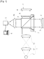
- FIG. 1 is a schematic view of a surface shape measuring system in accordance with the present invention.
- the surface shape measuring system of the present invention includes an illumination unit 1, a beam splitter 2, a light detecting element 5, and a subsidiary light source 7.
- the illumination unit 1 includes a main light source 11, a focusing lens 12 to focus light from the main light source 11, and a projection lens 13 to project the focused light from the focusing lens 12 to the beam splitter 2.
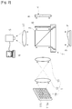
- FIG. 2 is a schematic view illustrating another embodiment of the illumination unit 1 of FIG. 1 .
- the illumination unit 1 includes a main light source 11 including an illumination panel 11 and a plurality of light emitting diodes 111 arranged in a matrix shape on the illumination panel 11'.
- the light emitting diodes 111 are divided into groups according to layers in the outward direction from the central light emitting diode 111a, and the turning-on of the light emitting diodes 111 is controlled according to the groups.
- the central light emitting diode 111a has a brightness value, which is higher than that of other peripheral light emitting diodes 111.
- two-dimensional inspection requires coaxial illumination having an area larger than that of an inspection region, and thus in the two-dimensional inspection, all the light emitting diodes 111 are turned on, or the plural layers of the light emitting diodes 111 are turned on.
- only the light emitting diode 111a is preferably turned on.
- FIG. 3 is a schematic view illustrating a further embodiment of the illumination unit 1 of FIG. 1 .
- the illumination unit 1 includes a main light source 11, a focusing lens 12, a projection lens 13, and an illumination panel 14.
- a plurality of light emitting diodes 142 arranged in a matrix shape is provided on the illumination panel 14, and a pin hole 141 is formed through the center of the illumination panel 14.
- two-dimensional inspection requires coaxial illumination having an area larger than that of an inspection region, and thus in the two-dimensional inspection, the main light source 11 and all the light emitting diodes 142 of the illumination panel 14 are turned on, or the plural layers of the light emitting diodes 142 are selectively turned on.
- only the main light source 11 is preferably turned on.
- FIG. 4 is a schematic view illustrating a still further embodiment of the illumination unit 1 of FIG. 1 .
- the illumination unit 1 includes a main light source 11, a microscope objective lens 12, and an illumination panel 14.
- a plurality of light emitting diodes 142 arranged in a matrix shape is provided on the illumination panel 14, and a pin hole 141 is formed through the center of the illumination panel 14.
- the main light source 11 and all the light emitting diodes 142 of the illumination panel 14 are turned on, and thus irradiate illumination light having an area larger than that of an inspection region onto the region.
- only the main light source 11 is preferably turned on such that light emitted from the main light source 11 passes through the microscope objective lens 12' thus increasing the visibility of an interference pattern while maintaining resolution.
- the microscope objective lens 12' which effectively focuses light on one point, is preferably used.
- the beam splitter 2 splits illumination light emitted from the illumination unit1 into beams respectively irradiated onto a reference surface (R) and a surface (R) of a target object to be measured, and the light detecting element 5 captures an image with an interference pattern.
- the light detecting element 5 captures the image with the interference pattern obtained by the interference of a reference beam and an object beam, which are respectively reflected by the reference surface (R) and the surface (R) of the object, and includes a projection lens 13.
- a control computer 6 obtains surface shape data through the analysis of the white-light interference pattern from the image captured by the light detecting element 5, and detects whether or not the object 3 is defective through the analysis of the obtained data.
- the subsidiary light source 7 is provided between the object 3 and the beam splitter 2, and provides falling illumination to the object 3.
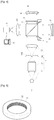
- the subsidiary light source 7, as shown in FIG. 5 includes a ring-shaped body 71, and a plurality of light emitting diodes 72 provided along the inner circumferential surface of the ring-shaped body 71.
- a mechanical shutter 8 to selectively intermit the irradiation of light onto the reference surface (R) is further provided between the beam splitter 2 and a reference mirror 4.
- the above surface shape measuring system obtains size data from an image captured after the irradiation of coaxial illumination through the turning-on of the main light source 11, and obtains surface defect data from an image captured after the irradiation of coaxial/falling illumination through the turning-on of the main light source 11 and the subsidiary light source 7, thus obtaining two-dimensional data regarding size and surface defect.
- three-dimensional inspection regions of the object are abstracted using the obtained two-dimensional data, and three-dimensional measurement only for the abstracted three-dimensional inspection regions is performed.
- three-dimensional data are obtained by generating an interference pattern through the formation of a reference beam and an object beam only for the abstracted three-dimensional inspection regions and capturing the interference pattern.
- two-dimensional data of a target object to be measured are obtained by selectively intermitting the turning-on of the main light source 11 and the subsidiary light source 7.
- coaxial/falling illumination is irradiated onto the surface (P) of the target object 3 by turning on the main light source 11 and the subsidiary light source 7 simultaneously, a second image is obtained by capturing the image of the surface (P) of the target object 3 using the light detecting element 5, and then whether or not the surface (P) of the target object 3 is defective is detected by analyzing the captured second image.
- the irradiation of light onto the reference surface (R) is cut off using the mechanical shutter 8.
- any one of the illumination units 1 of FIGS. 2 to 4 since the light emitting diodes arranged in a matrix shape are divided into groups according to layers, it is preferable that the turning-on of the light emitting diodes in the respective groups is selectively controlled according to a desired area or brightness.
- Inspection regions, for which three-dimensional inspection is performed, is abstracted using the above obtained two-dimensional data regarding the size and surface defect of the target object.
- regions requiring three-dimensional inspection such as regions "A"
- regions requiring three-dimensional inspection such as regions "A”
- regions "A” are abstracted
- an interference pattern of a reference beam and an object beam for the corresponding regions is generated and then three-dimensional shape inspection is performed. Thereby, an inspection speed is increased.
- the subsidiary light source 7 is turned off and only the main light source 11 is turned on, and the mechanical shutter 8 is opened such that light emitted from the main light source 11 is respectively irradiated onto the reference surface (R) and the measurement surface (P).
- the light is reflected by the reference surface (R) and the measurement surface (P), and thus produces a reference beam and an object beam.
- An interference pattern formed by the interference of the reference beam and the object beam is captured by the light detecting element 5.
- the height of the target object 3 or the distance of the reference mirror is properly adjusted using a fine driving unit (not shown), such as a PZT actuator.
- the main light source 11 includes a plurality of the light emitting diodes 111 arranged in a matrix shape, as shown in FIG. 2 , only the central light emitting diode 111a having a brightness value, which is higher than that of other peripheral light emitting diodes 111, is preferably turned on in three-dimensional inspection so as to increase an interference pattern generating capacity.
- the surface shape measuring system of the present invention includes the main light source and the subsidiary light source respectively providing coaxial illumination and falling illumination to a target object to be measured, obtains two-dimensional data by selectively intermitting the turning-on of the respective light sources and cutting off the irradiation of light onto the reference surface, abstracts three-dimensional inspection regions of the target object from the obtained two-dimensional data, and performs three-dimensional inspection only for the abstracted inspection regions.
- the surface shape measuring system of the present invention obtains both the two-dimensional data and the three-dimensional data of the target object using a single apparatus, thereby being capable of simplifying the apparatus.
- the surface shape measuring system of the present invention obtains the two-dimensional data of the target object in advance, abstracts the three-dimensional inspection regions of the target object from the obtained two-dimensional data, and obtains three-dimensional data only for the corresponding regions, thereby being capable of improving an inspection speed.
Landscapes
- Physics & Mathematics (AREA)
- General Physics & Mathematics (AREA)
- Engineering & Computer Science (AREA)
- Theoretical Computer Science (AREA)
- Optics & Photonics (AREA)
- Computer Vision & Pattern Recognition (AREA)
- Computer Graphics (AREA)
- Geometry (AREA)
- Software Systems (AREA)
- Length Measuring Devices By Optical Means (AREA)
- Instruments For Measurement Of Length By Optical Means (AREA)
Description
- The present invention relates to a surface shape measuring system and a surface shape measuring method using the same, and more particularly to a surface shape measuring system, in which both two-dimensional data and three-dimensional data of a target object to be measured are obtained using a single apparatus using white-light scanning interferometry and three-dimensional inspection is performed only for specific regions of the target object rather than the overall dimensions of the target object, and a surface shape measuring method using the same.
- Recently, in order to inspect the processed and manufactured state of a fine structure having a complicated stepped structure due to miniaturization and refinement of electronic and mechanical parts, a high measurement accuracy to size, shape, and surface roughness has been required.
- Therefore, a size measuring method using an optical two-dimensional measuring apparatus and a shape or a thickness (surface roughness) measuring method using an optical three-dimensional measuring apparatus are used now in measurement of small-sized electronic and mechanical parts.
- As one of conventional optical three-dimensional measuring apparatuses, white-light scanning interferometry (WSI) has been proposed.
-
US 2005/0206889 A1 discloses an optical fiber inspection device capable of performing a 2D visual inspection and a 3D interferometric measurement by operating a shutter associated with a reference mirror. -
US 7095507 B1 discloses an optical wafer inspection device capable of performing a 2D visual inspection and a 3D interferometric measurement by operating a shutter associated with a reference mirror. - With reference to
FIG. 7 , the WSI uses a principle, in which when a reference beam and an object beam obtained by splitting light generated from alight source 100 by abeam splitter 200 are respectively reflected by a reference surface of areference mirror 400 and a measurement surface (P) of atarget object 300 to be measured, and generate an interference signal, alight detecting element 500 captures the interference signal and then analyzes the signal. That is, the WSI measures a three-dimensional shape by detecting a position using a characteristic, in which the interference signal is generated only when the reference beam and the object beam pass through the same optical path. - When interference signals at respective measurement points within a measurement region are observed using the above principle while moving the object at minute intervals in the optical axial direction with a transfer unit, such as a PZT actuator, a short interference signal is generated at a position of each of the points, where the measurement beam has the same optical path as that of the reference beam.
- Therefore, when the interference signal generating positions of all the measurement points within the measurement region are calculated, data regarding the three-dimensional shape of the measurement surface are obtained, and thickness and shape of a thin film layer are measured from the obtained three-dimensional shape data.
- A measuring apparatus using white-light scanning interferometry is used in the measurement of the film thickness of a dielectric multi-layered film or the analysis of the structure of a continuum (diffuser), for example, the eye ground or the skin, as well as in the measurement of the three-dimensional shape of a fine structure.
- However, with the conventional measuring apparatuses, the two-dimensional measuring apparatus to measure the size of a target object to be measured and the three-dimensional measuring apparatus to measure the shape and thickness (surface roughness) of the object are independently designed and separately used, and thus are alternately used to measure the two-dimensional size and the three-dimensional shape of the object, thereby causing troublesomeness.
- Further, in case that the conventional three-dimensional measuring apparatus is used, the three-dimensional measuring apparatus obtains an interference pattern by scanning the overall dimensions of a target object to be measured and detects whether or not the object is defective using the interference pattern, and thus has a low inspection speed.
- Therefore, the present invention has been made in view of the above problems, and it is an object of the present invention to provide a surface shape measuring system using white-light scanning interferometry, in which two-dimensional data through the size measurement and surface defect inspection of a target object to be measured are obtained and three-dimensional data regarding the shape and thickness of the target object are obtained using a single apparatus, and a surface shape measuring method using the same.
- It is another object of the present invention to provide a surface shape measuring system using white-light scanning interferometry, in which two-dimensional data of a target object to be measured are obtained by selectively irradiating coaxial illumination and coaxial/falling illumination using a single apparatus, three-dimensional inspection regions of the target object are abstracted from the obtained two-dimensional data, and three-dimensional measurement is selectively performed only for the abstracted inspection regions, so as to simplify the apparatus and increase an inspection speed, and a surface shape measuring method using the same.
- In accordance with an aspect of the present invention, the above and other objects can be accomplished by the provision of a surface shape measuring system according to
claim 1. - In accordance with another aspect of the present invention, there is provided a surface shape measuring method according to claim 10.
- The above and other objects, features and other advantages of the present invention will be more clearly understood from the following detailed description taken in conjunction with the accompanying drawings, in which:
-
FIG. 1 is a schematic view of a surface shape measuring system in accordance with the present invention -
FIGS. 2 to 4 are schematic views illustrating modified embodiments of an illumination unit of the system ofFIG. 1 ; -
FIG. 5 is a perspective view illustrating an embodiment of a subsidiary light source of the system ofFIG. 1 ; -
FIG. 6 is an exemplary view illustrating an embodiment of a surface shape measuring method in accordance with the present invention and -
FIG. 7 is a schematic view of a conventional surface shape measuring system using white-light scanning interferometry. - Now, preferred embodiments of the present invention will be described in detail with reference to the annexed drawings.
-
FIG. 1 is a schematic view of a surface shape measuring system in accordance with the present invention. - With reference to
FIG. 1 , the surface shape measuring system of the present invention includes anillumination unit 1, abeam splitter 2, alight detecting element 5, and asubsidiary light source 7. - The
illumination unit 1 includes amain light source 11, a focusinglens 12 to focus light from themain light source 11, and aprojection lens 13 to project the focused light from the focusinglens 12 to thebeam splitter 2. -
FIG. 2 is a schematic view illustrating another embodiment of theillumination unit 1 ofFIG. 1 . Here, theillumination unit 1 includes amain light source 11 including anillumination panel 11 and a plurality oflight emitting diodes 111 arranged in a matrix shape on the illumination panel 11'. - The
light emitting diodes 111 are divided into groups according to layers in the outward direction from the centrallight emitting diode 111a, and the turning-on of thelight emitting diodes 111 is controlled according to the groups. - Further, the central
light emitting diode 111a has a brightness value, which is higher than that of other peripherallight emitting diodes 111. - That is, two-dimensional inspection requires coaxial illumination having an area larger than that of an inspection region, and thus in the two-dimensional inspection, all the
light emitting diodes 111 are turned on, or the plural layers of thelight emitting diodes 111 are turned on. - Further, in three-dimensional inspection, in order to supply illumination near to a point light source, which favorably generates an interference pattern, only the
light emitting diode 111a is preferably turned on. -
FIG. 3 is a schematic view illustrating a further embodiment of theillumination unit 1 ofFIG. 1 . Here, theillumination unit 1 includes amain light source 11, a focusinglens 12, aprojection lens 13, and anillumination panel 14. - A plurality of
light emitting diodes 142 arranged in a matrix shape is provided on theillumination panel 14, and apin hole 141 is formed through the center of theillumination panel 14. - In the above configuration, two-dimensional inspection requires coaxial illumination having an area larger than that of an inspection region, and thus in the two-dimensional inspection, the
main light source 11 and all thelight emitting diodes 142 of theillumination panel 14 are turned on, or the plural layers of thelight emitting diodes 142 are selectively turned on. - Further, in three-dimensional inspection, in order to supply illumination near to a point light source, which favorably generates an interference pattern, only the
main light source 11 is preferably turned on. -
FIG. 4 is a schematic view illustrating a still further embodiment of theillumination unit 1 ofFIG. 1 . Here, theillumination unit 1 includes amain light source 11, a microscopeobjective lens 12, and anillumination panel 14. - A plurality of
light emitting diodes 142 arranged in a matrix shape is provided on theillumination panel 14, and apin hole 141 is formed through the center of theillumination panel 14. - In two-dimensional inspection, the
main light source 11 and all thelight emitting diodes 142 of theillumination panel 14 are turned on, and thus irradiate illumination light having an area larger than that of an inspection region onto the region. - Further, in three-dimensional inspection, only the
main light source 11 is preferably turned on such that light emitted from themain light source 11 passes through the microscope objective lens 12' thus increasing the visibility of an interference pattern while maintaining resolution. - That is, when a light source emits light having a narrow wavelength or is near to a point light source, such as a laser source, an interference pattern is favorably generated, and when the light source emits light having a high wavelength, resolution is lowered. Thus, the microscope objective lens 12' which effectively focuses light on one point, is preferably used.
- The
beam splitter 2 splits illumination light emitted from the illumination unit1 into beams respectively irradiated onto a reference surface (R) and a surface (R) of a target object to be measured, and thelight detecting element 5 captures an image with an interference pattern. - That is, the
light detecting element 5 captures the image with the interference pattern obtained by the interference of a reference beam and an object beam, which are respectively reflected by the reference surface (R) and the surface (R) of the object, and includes aprojection lens 13. - Further, a
control computer 6 obtains surface shape data through the analysis of the white-light interference pattern from the image captured by thelight detecting element 5, and detects whether or not theobject 3 is defective through the analysis of the obtained data. - The
subsidiary light source 7 is provided between theobject 3 and thebeam splitter 2, and provides falling illumination to theobject 3. - The
subsidiary light source 7, as shown inFIG. 5 , includes a ring-shaped body 71, and a plurality oflight emitting diodes 72 provided along the inner circumferential surface of the ring-shaped body 71. - Preferably, a
mechanical shutter 8 to selectively intermit the irradiation of light onto the reference surface (R) is further provided between thebeam splitter 2 and areference mirror 4. - The above surface shape measuring system obtains size data from an image captured after the irradiation of coaxial illumination through the turning-on of the
main light source 11, and obtains surface defect data from an image captured after the irradiation of coaxial/falling illumination through the turning-on of themain light source 11 and thesubsidiary light source 7, thus obtaining two-dimensional data regarding size and surface defect. - Further, three-dimensional inspection regions of the object are abstracted using the obtained two-dimensional data, and three-dimensional measurement only for the abstracted three-dimensional inspection regions is performed.
- That is, three-dimensional data are obtained by generating an interference pattern through the formation of a reference beam and an object beam only for the abstracted three-dimensional inspection regions and capturing the interference pattern.
- Hereinafter, a surface shape measuring method using the surface shape measuring system of the present invention will be described.
- First, two-dimensional data of a target object to be measured are obtained by selectively intermitting the turning-on of the
main light source 11 and thesubsidiary light source 7. - That is, only coaxial illumination is irradiated onto the surface (P) of the
target object 3 by turning on themain light source 11, a first image is obtained by capturing the image of the surface (P) of thetarget object 3 using thelight detecting element 5, and then a size of the target object is measured by analyzing the captured first image. At this time, thesubsidiary light source 7 is turned off, and the irradiation of light onto the reference surface (R) is cut off using themechanical shutter 8. - Thereafter, coaxial/falling illumination is irradiated onto the surface (P) of the
target object 3 by turning on themain light source 11 and thesubsidiary light source 7 simultaneously, a second image is obtained by capturing the image of the surface (P) of thetarget object 3 using thelight detecting element 5, and then whether or not the surface (P) of thetarget object 3 is defective is detected by analyzing the captured second image. At this time, the irradiation of light onto the reference surface (R) is cut off using themechanical shutter 8. - Here, in case that any one of the
illumination units 1 ofFIGS. 2 to 4 is used, since the light emitting diodes arranged in a matrix shape are divided into groups according to layers, it is preferable that the turning-on of the light emitting diodes in the respective groups is selectively controlled according to a desired area or brightness. - Inspection regions, for which three-dimensional inspection is performed, is abstracted using the above obtained two-dimensional data regarding the size and surface defect of the target object.
- For example, as shown in
FIG. 6 , two-dimensional data for the overall surface of the target object are obtained, and regions requiring three-dimensional inspection, such as regions "A", are abstracted, and an interference pattern of a reference beam and an object beam for the corresponding regions is generated and then three-dimensional shape inspection is performed. Thereby, an inspection speed is increased. - Now, the three-dimensional shape inspection using white-light scanning interferometry, which analyzes an interference pattern generated by the interference of the reference beam and the object beam respectively reflected by the reference surface (R) and the measurement surface (P), will be described in brief.
- First, the subsidiary
light source 7 is turned off and only the mainlight source 11 is turned on, and themechanical shutter 8 is opened such that light emitted from the mainlight source 11 is respectively irradiated onto the reference surface (R) and the measurement surface (P). - Then, the light is reflected by the reference surface (R) and the measurement surface (P), and thus produces a reference beam and an object beam. An interference pattern formed by the interference of the reference beam and the object beam is captured by the
light detecting element 5. - Since the interference pattern formed by the interference of the reference beam and the object beam is obtained when the interference beam and the object beam have the same optical path, it is preferable that the height of the
target object 3 or the distance of the reference mirror is properly adjusted using a fine driving unit (not shown), such as a PZT actuator. - In case that the main
light source 11 includes a plurality of thelight emitting diodes 111 arranged in a matrix shape, as shown inFIG. 2 , only the centrallight emitting diode 111a having a brightness value, which is higher than that of other peripherallight emitting diodes 111, is preferably turned on in three-dimensional inspection so as to increase an interference pattern generating capacity. - As described above, the surface shape measuring system of the present invention includes the main light source and the subsidiary light source respectively providing coaxial illumination and falling illumination to a target object to be measured, obtains two-dimensional data by selectively intermitting the turning-on of the respective light sources and cutting off the irradiation of light onto the reference surface, abstracts three-dimensional inspection regions of the target object from the obtained two-dimensional data, and performs three-dimensional inspection only for the abstracted inspection regions. Thus, the surface shape measuring system of the present invention obtains both the two-dimensional data and the three-dimensional data of the target object using a single apparatus, thereby being capable of simplifying the apparatus.
- Further, the surface shape measuring system of the present invention obtains the two-dimensional data of the target object in advance, abstracts the three-dimensional inspection regions of the target object from the obtained two-dimensional data, and obtains three-dimensional data only for the corresponding regions, thereby being capable of improving an inspection speed.
Claims (11)
- A surface shape measuring system, comprising:an illumination unit (1) including a main light source (11), a focusing lens (12), and a projection lens (13);a beam splitter (2) to split illumination light emitted from the illumination unit (1) into beams respectively irradiated onto a reference surface (R) of a reference mirror and a measurement surface (P) of a target object to be measured;a light detecting element (5) to capture an interference pattern generated by the interference of a reference beam and an object beam respectively reflected by the reference surface (R) and the measurement surface (P);a control computer (6) to obtain surface shape data through white-light interference pattern analysis from an image captured by the light detecting element (5) and detect whether or not the measurement surface is defective from the obtained data, and:a subsidiary light source (7) to provide falling illumination to the target object (3), provided between the target object and the beam splitter (2);the control computer being configured to carry out the following steps :- obtaining two-dimensional data regarding the surface of the target object from size data through a first image captured using coaxial illumination, said coaxial illumination including the main light source being turned on and the subsidiary source being turned off, and from surface defect data through a second image captured using coaxial/falling illumination, said coaxial/falling illumination including the main light source and the subsidiary light source being turned on simultaneously, both the coaxial and the coaxial/falling illuminations including an irradiation of the illumination light onto the reference surface (R) being cut off (8);- abstracting three-dimensional inspection regions of the target object using the two-dimensional data; and- obtaining three-dimensional data regarding the surface shape of the target object by supplying the illumination light onto the reference surface (R),said obtaining of three-dimensional data being performed only for the abstracted three-dimensional inspection regions.
- The surface shape measuring system according to claim 1, wherein a mechanical shutter (8) configured to selectively cut off the irradiation of the illumination light onto the reference surface (R) is provided between the beam splitter (2) and the reference mirror (4).
- The surface shape measuring system according to claim 1 or 2, wherein the subsidiary light source (7) includes:a ring-shaped body (71); anda plurality of light emitting diodes (72) provided along the inner circumferential surface of the ring-shaped body (71) .
- The surface shape measuring system according to claim 1, wherein the main light source (11) includes:an illumination panel (11'); anda plurality of light emitting diodes (111) arranged in a matrix shape on the illumination panel.
- The surface shape measuring system according to claim 4, wherein the plurality of light emitting diodes (111) is divided into groups according to layers in the outward direction from a central light emitting diode (111a) such that the turning-on of the plurality of light emitting diodes is controllable according to the groups.
- The surface shape measuring system according to claim 5, wherein the central light emitting diode (111a) among the plurality of light emitting diodes (111) has a brightness value being higher than that of other peripheral light emitting diodes.
- The surface shape measuring system according to claim 1, wherein the illumination unit (1) further includes:an illumination panel (14) formed between the focusing lens (12) and the projection lens (13), and provided with a pin hole (141) formed through the center of the illumination panel (14); anda plurality of light emitting diodes (142) arranged in a matrix shape on the illumination panel.
- The surface shape measuring system according to claim 7, wherein the plurality of light emitting diodes (142) is divided into groups according to layers in the outward direction from a central light emitting diode such that the turning-on of the plurality of light emitting diodes is controllable according to the groups.
- The surface shape measuring system according to claim 7 or 8, wherein the focusing lens (12) is a microscope objective lens (12').
- A surface shape measuring method, in which illumination light emitted from a main light source (11) is split into beams, respectively irradiated onto a reference surface (R) of a reference mirror and a measurement surface (P) of a target object (3) to be measured, by a beam splitter (2), comprising:obtaining two-dimensional data of the target object by cutting off the supply of the illumination light onto the reference surface, said obtaining of the two-dimensional data including : obtaining size data of the target object using coaxial illumination including the main light source being turned on and a subsidiary light source, provided between the beam splitter and the target object, being turned off ; and obtaining surface defect data using coaxial/falling illumination including the main light source and the subsidiary light source being turned on simultaneously ;abstracting three-dimensional inspection regions from the obtained two-dimensional data; andobtaining three-dimensional data of the target object by generating an interference pattern for each of the abstracted inspection regions and capturing the interference pattern, said interference pattern being generated by the interference of a reference beam and an object beam respectively reflected by the reference surface and the measurement surface.
- The surface shape measuring method according to claim 10, wherein in the obtaining of the two-dimensional data, a cutting off of the supply of the illumination light onto the reference surface is selectively carried out through the intermission of a mechanical shutter (8).
Applications Claiming Priority (2)
| Application Number | Priority Date | Filing Date | Title |
|---|---|---|---|
| KR1020070131395A KR100939537B1 (en) | 2007-12-14 | 2007-12-14 | Surface shape measuring system and measuring method using the same |
| PCT/KR2008/007314 WO2009078617A2 (en) | 2007-12-14 | 2008-12-10 | Surface shape measuring system and surface shape measuring method using the same |
Publications (3)
| Publication Number | Publication Date |
|---|---|
| EP2220456A2 EP2220456A2 (en) | 2010-08-25 |
| EP2220456A4 EP2220456A4 (en) | 2016-08-03 |
| EP2220456B1 true EP2220456B1 (en) | 2019-11-20 |
Family
ID=40795998
Family Applications (1)
| Application Number | Title | Priority Date | Filing Date |
|---|---|---|---|
| EP08863179.1A Active EP2220456B1 (en) | 2007-12-14 | 2008-12-10 | Surface shape measuring system and surface shape measuring method using the same |
Country Status (6)
| Country | Link |
|---|---|
| US (1) | US8259305B2 (en) |
| EP (1) | EP2220456B1 (en) |
| JP (1) | JP5356402B2 (en) |
| KR (1) | KR100939537B1 (en) |
| TW (1) | TWI388796B (en) |
| WO (1) | WO2009078617A2 (en) |
Families Citing this family (24)
| Publication number | Priority date | Publication date | Assignee | Title |
|---|---|---|---|---|
| US8432395B2 (en) | 2009-06-16 | 2013-04-30 | Apple Inc. | Method and apparatus for surface contour mapping |
| KR101142763B1 (en) * | 2009-11-04 | 2012-05-18 | 한양대학교 산학협력단 | Spectro reflectometer and method for measuring spectro reflectance using the same |
| CN102822666A (en) * | 2009-11-30 | 2012-12-12 | 株式会社尼康 | Inspection device, three-dimensional shape measuring device, and manufacturing method of structure |
| TWI408331B (en) * | 2009-12-17 | 2013-09-11 | Ind Tech Res Inst | Measurement device and method of double-sided optical films |
| TW201129772A (en) * | 2010-02-26 | 2011-09-01 | Jian-Hong Liu | Measurement system for knife tip and diameter of miniature knife tool |
| JP5721420B2 (en) | 2010-12-17 | 2015-05-20 | キヤノン株式会社 | Measuring method and measuring device |
| TW201326737A (en) * | 2011-12-30 | 2013-07-01 | Metal Ind Res & Dev Ct | Measuring system and method for morphology of hole surface |
| KR101239409B1 (en) * | 2012-07-12 | 2013-03-05 | 주식회사 엠엠티 | 2d shape and 3d shape measuring apparatus and method based on phase shifting interferometry |
| CN102788558B (en) * | 2012-07-30 | 2014-12-10 | 山东师范大学 | Three-dimensional deformation measuring system and three-dimensional deformation measuring method combining speckle correlation and speckle interference |
| KR101462848B1 (en) * | 2013-03-18 | 2014-11-18 | 에스엔유 프리시젼 주식회사 | Three dimensional shape measurment apparatus for recogniting color |
| KR102369792B1 (en) | 2015-03-05 | 2022-03-03 | 한화테크윈 주식회사 | Photographing apparatus and photographing method |
| KR101628761B1 (en) * | 2015-03-06 | 2016-06-09 | (주) 인텍플러스 | surface shape measuring appatstus using asymmetric interferometer |
| KR20170028092A (en) * | 2015-09-03 | 2017-03-13 | 주식회사 이오테크닉스 | Apparatus and method for measuring thickness or height variation of object |
| KR20180007539A (en) * | 2016-07-13 | 2018-01-23 | 주식회사 메디트 | Path Length Multiplier of light for Three dimensional surface measuring |
| CN106441152B (en) * | 2016-10-18 | 2019-02-01 | 淮阴师范学院 | Asymmetric optical interferometry method and device |
| CN108662985B (en) * | 2017-03-30 | 2020-12-11 | 均豪精密工业股份有限公司 | Surface profile scanning method and device |
| TWI688748B (en) * | 2017-03-30 | 2020-03-21 | 均豪精密工業股份有限公司 | Method of scanning surface profile and apparatus thereof |
| CN110514142B (en) * | 2019-09-29 | 2020-09-08 | 中国科学院长春光学精密机械与物理研究所 | Surface shape detection device and surface shape detection method |
| CN113465534B (en) * | 2021-06-25 | 2022-04-19 | 浙江大学 | Micro-nano deep groove structure rapid measurement method based on white light interference |
| KR102660179B1 (en) * | 2021-12-22 | 2024-04-24 | 주식회사 휴비츠 | Calibration method of optical coherence tomography device and camera |
| DE112023000852T5 (en) * | 2022-02-07 | 2024-12-05 | Tokyo Seimitsu Co., Ltd. | Measuring device for a three-dimensional shape, method for setting a reference surface position therefor and method for switching a measuring mode therefor |
| KR102786771B1 (en) * | 2022-04-22 | 2025-03-31 | 주식회사 카이스 | Inspection apparatus for displacement measurement and visual acquisition at the same time |
| CN116708752B (en) * | 2022-10-28 | 2024-02-27 | 荣耀终端有限公司 | Imaging effect testing method, device and system for imaging device |
| WO2024238875A2 (en) * | 2023-05-18 | 2024-11-21 | Carnegie Mellon University | System and method for swept-angle interferometry |
Family Cites Families (23)
| Publication number | Priority date | Publication date | Assignee | Title |
|---|---|---|---|---|
| JPH0616087B2 (en) * | 1987-09-22 | 1994-03-02 | スタンレー電気株式会社 | Photoelectric detector |
| JP2732123B2 (en) * | 1989-06-19 | 1998-03-25 | 旭光学工業株式会社 | Pattern inspection equipment |
| JPH03209154A (en) * | 1990-01-11 | 1991-09-12 | Narumi China Corp | Automatic appearance checking device |
| JP2974393B2 (en) * | 1990-10-25 | 1999-11-10 | オリンパス光学工業株式会社 | Microscope image input device |
| JPH09250905A (en) * | 1996-01-10 | 1997-09-22 | Olympus Optical Co Ltd | Image measuring optical system |
| JPH109825A (en) | 1996-06-21 | 1998-01-16 | Komatsu Ltd | Confocal optics |
| US5777740A (en) * | 1997-02-27 | 1998-07-07 | Phase Metrics | Combined interferometer/polarimeter |
| JPH10239589A (en) * | 1997-02-28 | 1998-09-11 | Olympus Optical Co Ltd | Interference microscope |
| JPH1194528A (en) * | 1997-09-17 | 1999-04-09 | Nippon Seiko Kk | Appearance inspection device |
| JPH11109253A (en) * | 1997-10-01 | 1999-04-23 | Olympus Optical Co Ltd | Interference microscope |
| JPH11108625A (en) * | 1997-10-06 | 1999-04-23 | Canon Inc | Surface shape measuring device |
| JP3315358B2 (en) * | 1997-12-02 | 2002-08-19 | 株式会社ミツトヨ | Lighting equipment for image processing and measuring machines |
| AU1412000A (en) * | 1998-11-30 | 2000-06-19 | Olympus Optical Co., Ltd. | Measuring instrument |
| JP2002009497A (en) * | 2000-06-23 | 2002-01-11 | Juki Corp | Lighting equipment |
| WO2003038410A1 (en) * | 2001-10-31 | 2003-05-08 | Olympus Corporation | Optical scanning type observation device |
| JP2003255256A (en) * | 2002-02-28 | 2003-09-10 | Moritex Corp | Optical scanning device |
| JPWO2004013572A1 (en) * | 2002-08-01 | 2006-06-22 | 旭硝子株式会社 | Curved shape inspection method and apparatus |
| JP2004077223A (en) * | 2002-08-13 | 2004-03-11 | Nikon Corp | Optical heterodyne interferometer |
| US7095507B1 (en) * | 2002-09-27 | 2006-08-22 | Kla-Tencor Technologies Corporation | Method and apparatus using microscopic and interferometric based detection |
| US7312859B2 (en) * | 2004-01-30 | 2007-12-25 | Promet International, Inc. | Optical fiber inspection device |
| JP2006071353A (en) * | 2004-08-31 | 2006-03-16 | Tokyo Seimitsu Co Ltd | Microscope device, appearance inspection device, semiconductor appearance inspection device, and sample illumination method in microscope device |
| KR100672818B1 (en) * | 2006-01-26 | 2007-01-22 | 주식회사 고영테크놀러지 | 3D shape measurement method |
| DE102006021557B3 (en) * | 2006-05-08 | 2007-07-12 | Carl Mahr Holding Gmbh | Device under test reproducing and/or measuring arrangement for micro system technology, has illumination device illuminating device under test whose light is kept away from reference path |
-
2007
- 2007-12-14 KR KR1020070131395A patent/KR100939537B1/en active Active
-
2008
- 2008-12-10 EP EP08863179.1A patent/EP2220456B1/en active Active
- 2008-12-10 JP JP2010537863A patent/JP5356402B2/en active Active
- 2008-12-10 WO PCT/KR2008/007314 patent/WO2009078617A2/en not_active Ceased
- 2008-12-10 US US12/747,763 patent/US8259305B2/en active Active
- 2008-12-10 TW TW097147944A patent/TWI388796B/en active
Non-Patent Citations (1)
| Title |
|---|
| None * |
Also Published As
| Publication number | Publication date |
|---|---|
| US8259305B2 (en) | 2012-09-04 |
| TW200930975A (en) | 2009-07-16 |
| WO2009078617A2 (en) | 2009-06-25 |
| WO2009078617A4 (en) | 2009-10-08 |
| EP2220456A4 (en) | 2016-08-03 |
| US20100259765A1 (en) | 2010-10-14 |
| KR20090063874A (en) | 2009-06-18 |
| KR100939537B1 (en) | 2010-02-03 |
| JP5356402B2 (en) | 2013-12-04 |
| TWI388796B (en) | 2013-03-11 |
| JP2011519016A (en) | 2011-06-30 |
| EP2220456A2 (en) | 2010-08-25 |
| WO2009078617A3 (en) | 2009-08-13 |
Similar Documents
| Publication | Publication Date | Title |
|---|---|---|
| US8259305B2 (en) | Surface shape measuring system and surface shape measuring method using the same | |
| CN101438127B (en) | Apparatus and method for a combined interferometric and image based geometric determination, particularly in the microsystem technology | |
| TWI610762B (en) | Processing device | |
| US8493570B2 (en) | Three-dimensional shape measuring apparatus | |
| JP2009511279A (en) | Real-time topography tracking of objects during laser processing | |
| JP6389081B2 (en) | Shape measuring device, coating device, and shape measuring method | |
| US20130235387A1 (en) | Three-dimensional measuring device and method | |
| US8772688B2 (en) | Autofocus device including line image forming unit and rotation unit that rotates line image | |
| JP2013167857A (en) | Microscope and inspection device | |
| JP2008030119A (en) | Method and apparatus for microfabrication of materials | |
| JP7487045B2 (en) | Laser Processing Equipment | |
| KR20150057997A (en) | Detecting apparatus | |
| KR100785802B1 (en) | Three-dimensional shape measuring device | |
| JP2013015428A (en) | Inspection device, inspection method and manufacturing method of semiconductor device | |
| US9513112B1 (en) | Three dimensional characterization of silicon wafer Vias from combined on-top microscopic and bottom-through laser fringes measurement | |
| JP2010170602A (en) | Lens decentration measuring method and lens assembly method | |
| CN111610534B (en) | Imaging device and imaging method | |
| JP6665028B2 (en) | Shape measuring device and coating device equipped with the same | |
| KR102869910B1 (en) | Optical device for 3d printer and 3d printer comprising it | |
| JP5576195B2 (en) | Autofocus device | |
| KR20140023792A (en) | Surface shape measuring equipment | |
| US20170292833A1 (en) | Apparatus for measuring three-dimensional shape using prism | |
| JP2018187684A (en) | Laser processing apparatus | |
| JP2010169473A (en) | Method of detecting optical axis position of lens and method of measuring eccentricity | |
| CN119173732A (en) | Measuring device based on combined optical 2D and 3D image acquisition methods |
Legal Events
| Date | Code | Title | Description |
|---|---|---|---|
| PUAI | Public reference made under article 153(3) epc to a published international application that has entered the european phase |
Free format text: ORIGINAL CODE: 0009012 |
|
| 17P | Request for examination filed |
Effective date: 20100610 |
|
| AK | Designated contracting states |
Kind code of ref document: A2 Designated state(s): AT BE BG CH CY CZ DE DK EE ES FI FR GB GR HR HU IE IS IT LI LT LU LV MC MT NL NO PL PT RO SE SI SK TR |
|
| AX | Request for extension of the european patent |
Extension state: AL BA MK RS |
|
| DAX | Request for extension of the european patent (deleted) | ||
| A4 | Supplementary search report drawn up and despatched |
Effective date: 20160705 |
|
| RIC1 | Information provided on ipc code assigned before grant |
Ipc: G01B 11/24 20060101AFI20160630BHEP |
|
| STAA | Information on the status of an ep patent application or granted ep patent |
Free format text: STATUS: EXAMINATION IS IN PROGRESS |
|
| 17Q | First examination report despatched |
Effective date: 20181102 |
|
| GRAP | Despatch of communication of intention to grant a patent |
Free format text: ORIGINAL CODE: EPIDOSNIGR1 |
|
| STAA | Information on the status of an ep patent application or granted ep patent |
Free format text: STATUS: GRANT OF PATENT IS INTENDED |
|
| INTG | Intention to grant announced |
Effective date: 20190607 |
|
| GRAS | Grant fee paid |
Free format text: ORIGINAL CODE: EPIDOSNIGR3 |
|
| GRAA | (expected) grant |
Free format text: ORIGINAL CODE: 0009210 |
|
| STAA | Information on the status of an ep patent application or granted ep patent |
Free format text: STATUS: THE PATENT HAS BEEN GRANTED |
|
| AK | Designated contracting states |
Kind code of ref document: B1 Designated state(s): AT BE BG CH CY CZ DE DK EE ES FI FR GB GR HR HU IE IS IT LI LT LU LV MC MT NL NO PL PT RO SE SI SK TR |
|
| REG | Reference to a national code |
Ref country code: GB Ref legal event code: FG4D |
|
| REG | Reference to a national code |
Ref country code: CH Ref legal event code: EP |
|
| REG | Reference to a national code |
Ref country code: IE Ref legal event code: FG4D |
|
| REG | Reference to a national code |
Ref country code: DE Ref legal event code: R096 Ref document number: 602008061689 Country of ref document: DE |
|
| REG | Reference to a national code |
Ref country code: AT Ref legal event code: REF Ref document number: 1204674 Country of ref document: AT Kind code of ref document: T Effective date: 20191215 |
|
| REG | Reference to a national code |
Ref country code: NL Ref legal event code: MP Effective date: 20191120 |
|
| REG | Reference to a national code |
Ref country code: LT Ref legal event code: MG4D |
|
| PG25 | Lapsed in a contracting state [announced via postgrant information from national office to epo] |
Ref country code: GR Free format text: LAPSE BECAUSE OF FAILURE TO SUBMIT A TRANSLATION OF THE DESCRIPTION OR TO PAY THE FEE WITHIN THE PRESCRIBED TIME-LIMIT Effective date: 20200221 Ref country code: NO Free format text: LAPSE BECAUSE OF FAILURE TO SUBMIT A TRANSLATION OF THE DESCRIPTION OR TO PAY THE FEE WITHIN THE PRESCRIBED TIME-LIMIT Effective date: 20200220 Ref country code: NL Free format text: LAPSE BECAUSE OF FAILURE TO SUBMIT A TRANSLATION OF THE DESCRIPTION OR TO PAY THE FEE WITHIN THE PRESCRIBED TIME-LIMIT Effective date: 20191120 Ref country code: ES Free format text: LAPSE BECAUSE OF FAILURE TO SUBMIT A TRANSLATION OF THE DESCRIPTION OR TO PAY THE FEE WITHIN THE PRESCRIBED TIME-LIMIT Effective date: 20191120 Ref country code: LT Free format text: LAPSE BECAUSE OF FAILURE TO SUBMIT A TRANSLATION OF THE DESCRIPTION OR TO PAY THE FEE WITHIN THE PRESCRIBED TIME-LIMIT Effective date: 20191120 Ref country code: LV Free format text: LAPSE BECAUSE OF FAILURE TO SUBMIT A TRANSLATION OF THE DESCRIPTION OR TO PAY THE FEE WITHIN THE PRESCRIBED TIME-LIMIT Effective date: 20191120 Ref country code: SE Free format text: LAPSE BECAUSE OF FAILURE TO SUBMIT A TRANSLATION OF THE DESCRIPTION OR TO PAY THE FEE WITHIN THE PRESCRIBED TIME-LIMIT Effective date: 20191120 Ref country code: FI Free format text: LAPSE BECAUSE OF FAILURE TO SUBMIT A TRANSLATION OF THE DESCRIPTION OR TO PAY THE FEE WITHIN THE PRESCRIBED TIME-LIMIT Effective date: 20191120 Ref country code: BG Free format text: LAPSE BECAUSE OF FAILURE TO SUBMIT A TRANSLATION OF THE DESCRIPTION OR TO PAY THE FEE WITHIN THE PRESCRIBED TIME-LIMIT Effective date: 20200220 |
|
| PG25 | Lapsed in a contracting state [announced via postgrant information from national office to epo] |
Ref country code: IS Free format text: LAPSE BECAUSE OF FAILURE TO SUBMIT A TRANSLATION OF THE DESCRIPTION OR TO PAY THE FEE WITHIN THE PRESCRIBED TIME-LIMIT Effective date: 20200320 Ref country code: HR Free format text: LAPSE BECAUSE OF FAILURE TO SUBMIT A TRANSLATION OF THE DESCRIPTION OR TO PAY THE FEE WITHIN THE PRESCRIBED TIME-LIMIT Effective date: 20191120 |
|
| PG25 | Lapsed in a contracting state [announced via postgrant information from national office to epo] |
Ref country code: DK Free format text: LAPSE BECAUSE OF FAILURE TO SUBMIT A TRANSLATION OF THE DESCRIPTION OR TO PAY THE FEE WITHIN THE PRESCRIBED TIME-LIMIT Effective date: 20191120 Ref country code: PT Free format text: LAPSE BECAUSE OF FAILURE TO SUBMIT A TRANSLATION OF THE DESCRIPTION OR TO PAY THE FEE WITHIN THE PRESCRIBED TIME-LIMIT Effective date: 20200412 Ref country code: EE Free format text: LAPSE BECAUSE OF FAILURE TO SUBMIT A TRANSLATION OF THE DESCRIPTION OR TO PAY THE FEE WITHIN THE PRESCRIBED TIME-LIMIT Effective date: 20191120 Ref country code: CZ Free format text: LAPSE BECAUSE OF FAILURE TO SUBMIT A TRANSLATION OF THE DESCRIPTION OR TO PAY THE FEE WITHIN THE PRESCRIBED TIME-LIMIT Effective date: 20191120 Ref country code: RO Free format text: LAPSE BECAUSE OF FAILURE TO SUBMIT A TRANSLATION OF THE DESCRIPTION OR TO PAY THE FEE WITHIN THE PRESCRIBED TIME-LIMIT Effective date: 20191120 |
|
| REG | Reference to a national code |
Ref country code: CH Ref legal event code: PL |
|
| REG | Reference to a national code |
Ref country code: AT Ref legal event code: MK05 Ref document number: 1204674 Country of ref document: AT Kind code of ref document: T Effective date: 20191120 |
|
| REG | Reference to a national code |
Ref country code: DE Ref legal event code: R097 Ref document number: 602008061689 Country of ref document: DE |
|
| REG | Reference to a national code |
Ref country code: BE Ref legal event code: MM Effective date: 20191231 |
|
| PG25 | Lapsed in a contracting state [announced via postgrant information from national office to epo] |
Ref country code: MC Free format text: LAPSE BECAUSE OF FAILURE TO SUBMIT A TRANSLATION OF THE DESCRIPTION OR TO PAY THE FEE WITHIN THE PRESCRIBED TIME-LIMIT Effective date: 20191120 Ref country code: SK Free format text: LAPSE BECAUSE OF FAILURE TO SUBMIT A TRANSLATION OF THE DESCRIPTION OR TO PAY THE FEE WITHIN THE PRESCRIBED TIME-LIMIT Effective date: 20191120 |
|
| PLBE | No opposition filed within time limit |
Free format text: ORIGINAL CODE: 0009261 |
|
| STAA | Information on the status of an ep patent application or granted ep patent |
Free format text: STATUS: NO OPPOSITION FILED WITHIN TIME LIMIT |
|
| 26N | No opposition filed |
Effective date: 20200821 |
|
| GBPC | Gb: european patent ceased through non-payment of renewal fee |
Effective date: 20200220 |
|
| PG25 | Lapsed in a contracting state [announced via postgrant information from national office to epo] |
Ref country code: FR Free format text: LAPSE BECAUSE OF NON-PAYMENT OF DUE FEES Effective date: 20200120 Ref country code: LU Free format text: LAPSE BECAUSE OF NON-PAYMENT OF DUE FEES Effective date: 20191210 Ref country code: IE Free format text: LAPSE BECAUSE OF NON-PAYMENT OF DUE FEES Effective date: 20191210 |
|
| PG25 | Lapsed in a contracting state [announced via postgrant information from national office to epo] |
Ref country code: LI Free format text: LAPSE BECAUSE OF NON-PAYMENT OF DUE FEES Effective date: 20191231 Ref country code: PL Free format text: LAPSE BECAUSE OF FAILURE TO SUBMIT A TRANSLATION OF THE DESCRIPTION OR TO PAY THE FEE WITHIN THE PRESCRIBED TIME-LIMIT Effective date: 20191120 Ref country code: SI Free format text: LAPSE BECAUSE OF FAILURE TO SUBMIT A TRANSLATION OF THE DESCRIPTION OR TO PAY THE FEE WITHIN THE PRESCRIBED TIME-LIMIT Effective date: 20191120 Ref country code: BE Free format text: LAPSE BECAUSE OF NON-PAYMENT OF DUE FEES Effective date: 20191231 Ref country code: CH Free format text: LAPSE BECAUSE OF NON-PAYMENT OF DUE FEES Effective date: 20191231 Ref country code: AT Free format text: LAPSE BECAUSE OF FAILURE TO SUBMIT A TRANSLATION OF THE DESCRIPTION OR TO PAY THE FEE WITHIN THE PRESCRIBED TIME-LIMIT Effective date: 20191120 |
|
| PG25 | Lapsed in a contracting state [announced via postgrant information from national office to epo] |
Ref country code: IT Free format text: LAPSE BECAUSE OF FAILURE TO SUBMIT A TRANSLATION OF THE DESCRIPTION OR TO PAY THE FEE WITHIN THE PRESCRIBED TIME-LIMIT Effective date: 20191120 Ref country code: GB Free format text: LAPSE BECAUSE OF NON-PAYMENT OF DUE FEES Effective date: 20200220 |
|
| PG25 | Lapsed in a contracting state [announced via postgrant information from national office to epo] |
Ref country code: CY Free format text: LAPSE BECAUSE OF FAILURE TO SUBMIT A TRANSLATION OF THE DESCRIPTION OR TO PAY THE FEE WITHIN THE PRESCRIBED TIME-LIMIT Effective date: 20191120 |
|
| PG25 | Lapsed in a contracting state [announced via postgrant information from national office to epo] |
Ref country code: MT Free format text: LAPSE BECAUSE OF FAILURE TO SUBMIT A TRANSLATION OF THE DESCRIPTION OR TO PAY THE FEE WITHIN THE PRESCRIBED TIME-LIMIT Effective date: 20191120 Ref country code: HU Free format text: LAPSE BECAUSE OF FAILURE TO SUBMIT A TRANSLATION OF THE DESCRIPTION OR TO PAY THE FEE WITHIN THE PRESCRIBED TIME-LIMIT; INVALID AB INITIO Effective date: 20081210 |
|
| PG25 | Lapsed in a contracting state [announced via postgrant information from national office to epo] |
Ref country code: TR Free format text: LAPSE BECAUSE OF FAILURE TO SUBMIT A TRANSLATION OF THE DESCRIPTION OR TO PAY THE FEE WITHIN THE PRESCRIBED TIME-LIMIT Effective date: 20191120 |
|
| PGFP | Annual fee paid to national office [announced via postgrant information from national office to epo] |
Ref country code: DE Payment date: 20251231 Year of fee payment: 18 |