EP2211227A1 - Display panel and method of manufacturing the same - Google Patents
Display panel and method of manufacturing the same Download PDFInfo
- Publication number
- EP2211227A1 EP2211227A1 EP09014582A EP09014582A EP2211227A1 EP 2211227 A1 EP2211227 A1 EP 2211227A1 EP 09014582 A EP09014582 A EP 09014582A EP 09014582 A EP09014582 A EP 09014582A EP 2211227 A1 EP2211227 A1 EP 2211227A1
- Authority
- EP
- European Patent Office
- Prior art keywords
- sensor wire
- data line
- substrate
- display panel
- sensor
- Prior art date
- Legal status (The legal status is an assumption and is not a legal conclusion. Google has not performed a legal analysis and makes no representation as to the accuracy of the status listed.)
- Granted
Links
Images


Classifications
-
- G—PHYSICS
- G06—COMPUTING; CALCULATING OR COUNTING
- G06F—ELECTRIC DIGITAL DATA PROCESSING
- G06F3/00—Input arrangements for transferring data to be processed into a form capable of being handled by the computer; Output arrangements for transferring data from processing unit to output unit, e.g. interface arrangements
- G06F3/01—Input arrangements or combined input and output arrangements for interaction between user and computer
- G06F3/03—Arrangements for converting the position or the displacement of a member into a coded form
- G06F3/041—Digitisers, e.g. for touch screens or touch pads, characterised by the transducing means
- G06F3/0412—Digitisers structurally integrated in a display
-
- G—PHYSICS
- G02—OPTICS
- G02F—OPTICAL DEVICES OR ARRANGEMENTS FOR THE CONTROL OF LIGHT BY MODIFICATION OF THE OPTICAL PROPERTIES OF THE MEDIA OF THE ELEMENTS INVOLVED THEREIN; NON-LINEAR OPTICS; FREQUENCY-CHANGING OF LIGHT; OPTICAL LOGIC ELEMENTS; OPTICAL ANALOGUE/DIGITAL CONVERTERS
- G02F1/00—Devices or arrangements for the control of the intensity, colour, phase, polarisation or direction of light arriving from an independent light source, e.g. switching, gating or modulating; Non-linear optics
- G02F1/01—Devices or arrangements for the control of the intensity, colour, phase, polarisation or direction of light arriving from an independent light source, e.g. switching, gating or modulating; Non-linear optics for the control of the intensity, phase, polarisation or colour
- G02F1/13—Devices or arrangements for the control of the intensity, colour, phase, polarisation or direction of light arriving from an independent light source, e.g. switching, gating or modulating; Non-linear optics for the control of the intensity, phase, polarisation or colour based on liquid crystals, e.g. single liquid crystal display cells
- G02F1/133—Constructional arrangements; Operation of liquid crystal cells; Circuit arrangements
- G02F1/136—Liquid crystal cells structurally associated with a semi-conducting layer or substrate, e.g. cells forming part of an integrated circuit
- G02F1/1362—Active matrix addressed cells
- G02F1/136286—Wiring, e.g. gate line, drain line
-
- G—PHYSICS
- G02—OPTICS
- G02F—OPTICAL DEVICES OR ARRANGEMENTS FOR THE CONTROL OF LIGHT BY MODIFICATION OF THE OPTICAL PROPERTIES OF THE MEDIA OF THE ELEMENTS INVOLVED THEREIN; NON-LINEAR OPTICS; FREQUENCY-CHANGING OF LIGHT; OPTICAL LOGIC ELEMENTS; OPTICAL ANALOGUE/DIGITAL CONVERTERS
- G02F1/00—Devices or arrangements for the control of the intensity, colour, phase, polarisation or direction of light arriving from an independent light source, e.g. switching, gating or modulating; Non-linear optics
- G02F1/01—Devices or arrangements for the control of the intensity, colour, phase, polarisation or direction of light arriving from an independent light source, e.g. switching, gating or modulating; Non-linear optics for the control of the intensity, phase, polarisation or colour
- G02F1/13—Devices or arrangements for the control of the intensity, colour, phase, polarisation or direction of light arriving from an independent light source, e.g. switching, gating or modulating; Non-linear optics for the control of the intensity, phase, polarisation or colour based on liquid crystals, e.g. single liquid crystal display cells
- G02F1/133—Constructional arrangements; Operation of liquid crystal cells; Circuit arrangements
- G02F1/1333—Constructional arrangements; Manufacturing methods
- G02F1/13338—Input devices, e.g. touch panels
-
- G—PHYSICS
- G02—OPTICS
- G02F—OPTICAL DEVICES OR ARRANGEMENTS FOR THE CONTROL OF LIGHT BY MODIFICATION OF THE OPTICAL PROPERTIES OF THE MEDIA OF THE ELEMENTS INVOLVED THEREIN; NON-LINEAR OPTICS; FREQUENCY-CHANGING OF LIGHT; OPTICAL LOGIC ELEMENTS; OPTICAL ANALOGUE/DIGITAL CONVERTERS
- G02F1/00—Devices or arrangements for the control of the intensity, colour, phase, polarisation or direction of light arriving from an independent light source, e.g. switching, gating or modulating; Non-linear optics
- G02F1/01—Devices or arrangements for the control of the intensity, colour, phase, polarisation or direction of light arriving from an independent light source, e.g. switching, gating or modulating; Non-linear optics for the control of the intensity, phase, polarisation or colour
- G02F1/13—Devices or arrangements for the control of the intensity, colour, phase, polarisation or direction of light arriving from an independent light source, e.g. switching, gating or modulating; Non-linear optics for the control of the intensity, phase, polarisation or colour based on liquid crystals, e.g. single liquid crystal display cells
- G02F1/133—Constructional arrangements; Operation of liquid crystal cells; Circuit arrangements
- G02F1/136—Liquid crystal cells structurally associated with a semi-conducting layer or substrate, e.g. cells forming part of an integrated circuit
- G02F1/1362—Active matrix addressed cells
- G02F1/136286—Wiring, e.g. gate line, drain line
- G02F1/13629—Multilayer wirings
-
- G—PHYSICS
- G02—OPTICS
- G02F—OPTICAL DEVICES OR ARRANGEMENTS FOR THE CONTROL OF LIGHT BY MODIFICATION OF THE OPTICAL PROPERTIES OF THE MEDIA OF THE ELEMENTS INVOLVED THEREIN; NON-LINEAR OPTICS; FREQUENCY-CHANGING OF LIGHT; OPTICAL LOGIC ELEMENTS; OPTICAL ANALOGUE/DIGITAL CONVERTERS
- G02F1/00—Devices or arrangements for the control of the intensity, colour, phase, polarisation or direction of light arriving from an independent light source, e.g. switching, gating or modulating; Non-linear optics
- G02F1/01—Devices or arrangements for the control of the intensity, colour, phase, polarisation or direction of light arriving from an independent light source, e.g. switching, gating or modulating; Non-linear optics for the control of the intensity, phase, polarisation or colour
- G02F1/13—Devices or arrangements for the control of the intensity, colour, phase, polarisation or direction of light arriving from an independent light source, e.g. switching, gating or modulating; Non-linear optics for the control of the intensity, phase, polarisation or colour based on liquid crystals, e.g. single liquid crystal display cells
- G02F1/133—Constructional arrangements; Operation of liquid crystal cells; Circuit arrangements
- G02F1/136—Liquid crystal cells structurally associated with a semi-conducting layer or substrate, e.g. cells forming part of an integrated circuit
- G02F1/1362—Active matrix addressed cells
- G02F1/136286—Wiring, e.g. gate line, drain line
- G02F1/136295—Materials; Compositions; Manufacture processes
-
- G—PHYSICS
- G06—COMPUTING; CALCULATING OR COUNTING
- G06F—ELECTRIC DIGITAL DATA PROCESSING
- G06F3/00—Input arrangements for transferring data to be processed into a form capable of being handled by the computer; Output arrangements for transferring data from processing unit to output unit, e.g. interface arrangements
- G06F3/01—Input arrangements or combined input and output arrangements for interaction between user and computer
- G06F3/03—Arrangements for converting the position or the displacement of a member into a coded form
- G06F3/041—Digitisers, e.g. for touch screens or touch pads, characterised by the transducing means
- G06F3/045—Digitisers, e.g. for touch screens or touch pads, characterised by the transducing means using resistive elements, e.g. a single continuous surface or two parallel surfaces put in contact
-
- G—PHYSICS
- G02—OPTICS
- G02F—OPTICAL DEVICES OR ARRANGEMENTS FOR THE CONTROL OF LIGHT BY MODIFICATION OF THE OPTICAL PROPERTIES OF THE MEDIA OF THE ELEMENTS INVOLVED THEREIN; NON-LINEAR OPTICS; FREQUENCY-CHANGING OF LIGHT; OPTICAL LOGIC ELEMENTS; OPTICAL ANALOGUE/DIGITAL CONVERTERS
- G02F2201/00—Constructional arrangements not provided for in groups G02F1/00 - G02F7/00
- G02F2201/40—Arrangements for improving the aperture ratio
Definitions
- the present invention relates to a display panel and a method of manufacturing the same, and more particularly to a display panel and a method of manufacturing the same, which can prevent the deterioration of the input sensitivity of the panel, and maximize the aperture ratio of the panel.
- a touch panel includes an input means which is installed on an image display surface of a liquid crystal display (LCD), a field emission display (FED), a plasma display panel (PDP), an electro luminescence display (ELD), and the like, and receives an input of information when a user presses a display screen.
- LCD liquid crystal display
- FED field emission display
- PDP plasma display panel
- ELD electro luminescence display
- a touch panel may be classified into a capacitive touch panel and a resistive touch panel.
- the capacitive touch panel operates in a manner that, in a state where the charge/discharge state of capacitance is repeated on a transparent conductive film or transparent conductive glass, a small amount of charge is accumulated between a stylus that is a pen type input means and the conductive film, this accumulated amount of charge is detected from an input point, and the detected amount of charge is converted into a coordinate value.
- the resistive touch panel operates such that when a user presses a screen, two opposite conductive films come in contact with each other while a voltage is applied to the conductive films. The change in voltage or current occurring at a contact point is detected, and a coordinate value of the contact point, which corresponds to the detected change of voltage or current, is read.
- the capacitive touch panel requires a supply of electricity to the stylus
- an analog input type resistive touch panel which is associated with a liquid crystal panel
- the resistive touch panel may be formed inside the liquid crystal display panel.
- first sensor lines and second sensor lines form a grid on a thin film transistor substrate to detect first coordinates of a horizontal position of an input point and second coordinates of a vertical position of the input point.
- Sensor spacers for contacting the first and second sensor lines may also be formed on a color filter substrate.
- the aperture ratio of a display panel is reduced by the first and second sensor lines. Furthermore, the sensitivity of the second sensor lines to the input pressure deteriorates due to the presence of data lines and gate lines in the display.
- An object of the present invention is to provide a display panel that can prevent the deterioration of the input pressure sensitivity of the panel, and maximize the aperture ratio of the panel.
- Another object of the present invention is to provide a method of manufacturing a display panel that can prevent the deterioration of the input sensitivity of the panel and maximize the aperture ratio of the panel.
- a display panel which includes a first substrate; a gate line and a data line crossing each other on the first substrate and electrically insulated from each other; a first sensor wire formed in parallel to the gate line; a second sensor wire formed to overlap the data line in parallel to the data line; a second substrate arranged opposite to the first substrate; and a sensor spacer formed on the second substrate to project toward the first substrate.
- a method of manufacturing a display panel which includes forming a second sensor wire on a first substrate; forming a first insulating layer on the second sensor wire; forming a gate line and a first sensor wire, which cross the second sensor wire, on the first insulating layer; forming a second insulating layer on the gate line and the first sensor wire; and forming a data line to overlap the second sensor wire in parallel to the second sensor wire.
- a method of manufacturing a display panel which includes forming a gate line and a first sensor wire that is in parallel to the gate line on a first substrate; forming a first insulating layer on the gate line and the first sensor wire; forming a data line, which crosses the gate line and the first sensor wire, on the first insulating layer; forming a second insulating layer on the data line; and forming a second sensor wire formed to overlap the data line in parallel to the data line.
- a method of manufacturing a display panel which includes forming a data line on a first substrate; forming a first insulating layer on the data line; forming a gate line and a first sensor wire, which cross the data line, on the first insulating layer; forming a second insulating layer on the gate line and the first senso wire; and forming a second sensor wire formed to overlap the data line in parallel to the data line.
- spatially relative words such as “below”, “beneath”, “lower”, “above”, “upper”, and so forth, as illustrated in the drawings, may be used to facilitate the description of relationships between an element or constituent elements, and another element or other constituent elements.
- the spatially relative words should be understood as words that include different directions of the element in use or operation, in addition to the direction illustrated in the drawings. For example, if an element illustrated in the drawing is turned over, the element described to be “below” or “beneath” another element may be put “above” the other element. Accordingly, the exemplary wording "below” may include both directions corresponding to "below” and "above”. An element may be aligned in a different direction, and thus the spatially relative words may be interpreted according to the alignment of the element.
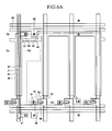
- FIG. 1 is a layout diagram of a display panel according to a first embodiment of the present invention.
- FIG. 2A is a sectional view of a display panel, taken along line IIa-IIa' in FIG. 1
- FIG. 2B is a sectional view of a display panel, taken along line IIb-IIb' in FIG. 1 .
- a display panel 1 according to the first embodiment of the present invention includes a lower substrate 2 and an upper substrate 3, which are formed opposite to each other, and a liquid crystal layer 4 interposed between the two substrates 2 and 3.
- the lower substrate 2 includes a gate line 41 formed on a first substrate 10, a first sensor wire 43, a data line 81, a second sensor wire 21, a blocking electrode 45, a thin film transistor (TFT), a pixel electrode 95, a first sensor pad 96, and a second sensor pad 97.
- a gate line 41 formed on a first substrate 10, a first sensor wire 43, a data line 81, a second sensor wire 21, a blocking electrode 45, a thin film transistor (TFT), a pixel electrode 95, a first sensor pad 96, and a second sensor pad 97.
- TFT thin film transistor
- the first substrate 10 is an insulating substrate having heat resistance and transparency, such as transparent glass or plastic.
- the second sensor wire 21 is formed, extended in a direction parallel to a data line 81, to be described later.
- the second sensor wire 21, for example, transfers a Y-coordinate signal.
- the first sensor wire 43 transfers an X-coordinate signal.
- a second sensor wire extension part 22 connected to the second sensor pad 97, is branched.
- a first insulating film 30 made of silicon nitride (SiNx) is formed on the second sensor wire 21 and the second sensor wire extension part 22, a first insulating film 30 made of silicon nitride (SiNx) is formed.
- the first sensor wire 43 and the gate line 41 which cross the second sensor wire 21, are formed.
- the first sensor wire 43 and the gate line 41 are insulated from the second sensor wire 21 by the first insulating film 30.
- the gate line 41 is formed on the first substrate 10 in a first direction, and transfers a gate signal to the thin film transistor (TFT).
- the first direction may be a horizontal direction of the first substrate 10.
- the gate line 41 may be formed as a single layer or a multi-layer made of any one of molybdenum (Mo), niobium (Nb), copper (Cu), aluminum (Al), chrome (Cr), silver (Ag), tungsten (W), titanium (Ti), and their alloys.
- One end part of the gate line 41 is branched to form an extended gate electrode 42.
- the first sensor wire 43 is formed in the first direction in parallel to the gate line 41.
- the first sensor wire 43 may be formed of the same material as the gate line 41 on the same layer as the gate line 41.
- the blocking electrode 45 is formed on the second sensor wire 21, the blocking electrode 45 is formed.
- the blocking electrode 45 overlaps the second sensor wire 21, and prevents the occurrence of interference between the second sensor wire 21 and the data line 81.
- the data signal being applied to the data line has a continuously changing waveform with a nonuniform voltage level.
- the data signal affects the second sensor wire 21, and thus it is required to form the blocking electrode 45 between the second sensor wire 21 and the data line 81.
- a DC voltage having the same voltage level as the common voltage may be applied to the blocking electrode 45.
- the blocking electrode 45 overlaps the pixel electrode 95 to be described later to form a storage capacitor.
- the blocking electrode 45 is connected to a storage electrode 46, which partially overlaps the pixel electrode 95.
- the second insulating film 50 is spread.
- the second insulating film can be made of silicon nitride (SiNx).
- a semiconductor layer 61 made of hydrogenated amorphous silicon or polycrystalline silicon is formed on the second insulating film 50.
- ohmic contact layers 75 and 76 made of silicide or n+ hydrogenated amorphous silicon, doped with high-density n-type impurities are formed on an upper part of the semiconductor layer 61.
- the ohmic contact layers 75 and 76 constitute a pair, and are positioned on the semiconductor layer 61.
- the data line 81, and a drain electrode 86 that corresponds to the data line 81 are formed.
- the data line 81 is formed on the first substrate 10 in a second direction, and transfers a data signal to each pixel.
- the second direction may be a vertical direction of the first substrate 10.
- the data line 41 may be formed as a single layer or a multi-layer made of a material selected from the group comprising at least one of the following: molybdenum (Mo), niobium (Nb), copper (Cu), aluminum (Al), chrome (Cr), silver (Ag), tungsten (W), titanium (Ti), and their alloys.
- the data line 81 is formed to overlap the second sensor wire 21. Both the data line 81 and the second sensor wire 21 are formed of an opaque metallic material. The data line 81 and the second sensor wire 21 reduce the aperture ratio of the display panel 1, by reducing the transparency of light. As used herein, the aperture ratio of the display panel is defined as ... The data line and the second sensor wire are formed of materials that have a reduced light transparency. Therefore, a person of ordinary skill in the art of designing and making display panels would recognize that, in general, the data line and the second sensor wire tend to reduce the aperture ratio of the display panel. Accordingly, by overlapping the data line 81 and the second sensor wire 21, a light blocking area is reduced, and thus the aperture ratio can be increased.
- a source electrode 85 extending toward the drain electrode 86 is formed on the data line 81.
- the drain electrode 86 transfers the data signal to the pixel electrode 95.
- the gate electrode 42, the source electrode 85, and the drain electrode 86 form three terminals of the thin film transistor (TFT).
- the thin film transistor (TFT) transfers the source electrode's input data signal to the pixel electrode 95 through the drain electrode 86, in response to the gate signal.
- the thin film transistor includes the semiconductor layer 61 that forms a channel between the source electrode 85 and the drain electrode 86 as it is interposed between and partially overlaps the gate electrode 42 and the second insulating film 50.
- a passivation film 90 is formed of an inorganic material such as silicon nitride (SiNx) or silicon oxide (SiOx), or an organic material such as acrylic, polyimide, or benzocyclobutene (BCB).
- the passivation film 90 may be a single layer or a multi-layer formed of an inorganic material and an organic material.
- the passivation film 90 is formed to cover the thin film transistor (TFT) and the second insulating film 50, and insulates the thin film transistor (TFT) and the pixel electrode 95.
- the passivation film 90 includes first to third contact holes 91, 92, and 93 for exposing the drain electrode 86, the first sensor wire 43 and the second sensor wire 21.
- the first to third contact holes 91, 92, and 93 are formed by etching a part of the passivation film 90 through a mask.
- the pixel electrode 95 is formed on the upper part of the passivation film 90.
- the pixel electrode 95 is connected to the drain electrode 86 of the thin film transistor (TFT) through the first contact hole 91.
- the pixel electrode 95 is made of a transparent conductive material, such as ITO (Indium Tin Oxide) or IZO (Indium Zinc Oxide), or a reflective conductive material such as aluminum.
- the first sensor pad 96 contacts a sensor electrode 152 to be described later, and provides a signal for recognizing an X-axis coordinate value to the first sensor wire 43.
- the first sensor pad 96 is connected to a first sensor wire extension part 44 branched from the first sensor wire 43 through the second contact hole 92.
- the second sensor pad 97 contacts the sensor electrode 152 to be described later, and provides a signal for recognizing a Y-axis coordinate value to the second sensor wire 21.
- the second sensor pad 97 is connected to the second sensor wire extension part 22 branched from the second sensor wire 21 through the third contact hole 93.
- the first sensor pad 96 and the second sensor pad 97 are formed to overlap a sensor spacer 140 to be described later and the sensor electrode 152.
- the first sensor pad 96 and the second sensor pad 97 may be formed of the same material as the pixel electrode 95 through the same process.
- the upper substrate 3 includes a black matrix 120 formed on the second substrate 110 to prevent light leakage, a color filter 130 for color representation, and a common electrode 151 applying a common voltage to the liquid crystal layer 4.
- the second substrate 110 may be formed of a transparent insulating material that transmits the light, and may be formed of a material, such as glass or plastic that is flexible in accordance with pressure being applied to the upper part thereof.
- the black matrix 120 may be formed to overlap the thin film transistor (TFT) of the lower substrate 2, the gate line 41, the data line 81, the first sensor wire 43, and the second sensor wire 21.
- the black matrix 120 may be formed of an opaque organic material, or opaque metal.
- the color filter 130 is composed of red, green, and blue color filters to represent colors.
- the color filter 130 represents red, green, and blue colors by absorbing or transmitting light of specified wavelengths through the red, green, and blue pigments included therein.
- the color filter represents diverse colors through the additive mixture of transmitted red, green, and blue colors.
- the common electrode 151 is formed on the upper parts of the color filter 130 and the black matrix 120.
- an overcoat layer (not illustrated) for reducing the unevenness of the color filters may be formed, and the common electrode 151 may be formed on the upper part of the overcoat layer.
- the common electrode 151 may be formed of a transparent conductive material such as ITO (Indium Tin Oxide) or IZO (Indium Zinc Oxide).
- the common electrode 151 applies an electric field for driving liquid crystals, which is formed by a difference between the common voltage being supplied from the common voltage generator and the voltage of the data signal of the pixel electrode 95, to the liquid crystal layer 4.
- the sensor spacer 140 may be formed on the black matrix 120. That is, the sensor spacer 140 is formed to overlap the black matrix 120 that does not transmit the light, and the sensor electrode 152 is formed on the sensor spacer 140.
- the sensor spacer 140 may be formed of an organic material in the same process as the organic material of the color filter 130. However, the forming of the sensor spacer 140 in the same process as the color filter 130 is merely exemplary, and the sensor spacer may be formed together with the overcoat layer (not illustrated) on the black matrix 120, or may be separately formed in an independent process.
- the sensor spacer 140 projects toward the first substrate 10.
- the sensor electrode 152 is formed on the sensor spacer 140. If a user applies pressure to a certain point of the upper substrate 3, the second substrate 110 is curved downward, and the sensor spacer 140 makes contact with the first sensor pad 96 and the second sensor pad 97, so that the pressed position can be recognized.
- the sensor spacer 140 and the first/second sensor pads 96 and 97 are spaced apart from each other for a specified distance.
- the sensor spacer 140 makes contact with the first sensor pad 96 and the second sensor pad 97.
- the resistance value of the segment of the first sensor wire and the segment of the second sensor wire in contact with the sensor electrode 152 is varied in accordance with the contact point.
- This variable resistance value causes a current or voltage difference, so that the X-coordinate signal is transmitted through the first sensor wire 43, and the Y-coordinate signal is transmitted through the second sensor wire 21.
- FIGS. 3A to 7C are process views explaining a process of manufacturing a lower substrate included in the display panel of FIG. 1 .
- the second sensor wire 21 is formed on the first substrate 10. Specifically, a sensor wire conduction layer is laminated on the first substrate 10 by sputtering. The sensor wire conduction layer is deposited on the front surface of the first substrate 10. Then, by photo-etching the sensor wire conduction layer, the second sensor wire 21 is formed. The second sensor wire 21 may be extended in a vertical direction of the first substrate 10.
- the first insulating layer 30 made of silicon nitride (SiNx) is formed on the second sensor wire 21.
- the gate line 41, the first sensor wire 43, and the blocking electrode 45 are formed on the first insulating film 30.
- a gate conduction layer is laminated on the front surface of the first insulating film 30, using a sputtering method.
- the gate line 41, the first sensor wire 43 and the blocking electrode 45 are formed by photo-etching the gate conduction layer.
- the gate line 41 and the first sensor wire 43 cross the second sensor wire 21, and are extended in the horizontal direction of the first substrate 10.
- the gate line 41 and the first sensor wire 43 are formed in parallel to each other.
- the blocking electrode 45 is formed between the gate wire 41 and the first sensor wire 43, and overlaps the second sensor wire 21.
- the blocking electrode 45 is connected to the storage electrode 46.
- the second insulating film 50 is formed by chemical vapor deposition (CVD).
- the semiconductor layer 61, the data line 81, the source electrode 85, and the drain electrode 86 are formed on the second insulating film 50.
- a first amorphous silicon layer made of hydrogenated amorphous silicon and a second amorphous silicon layer made of silicide or n+ hydrogenated amorphous silicon, doped with high-density n-type impurities are laminated in sequence.
- the lamination of the first amorphous silicon layer and the second amorphous silicon layer may be performed by chemical vapor deposition (CVD).
- the first amorphous silicon layer and the second amorphous silicon layer, except for an area where an active layer is formed on the gate electrode 42 of each pixel, are removed by photo-etching.
- the first amorphous silicon layer is etched to form the semiconductor layer 61, and the second amorphous silicon layer is etched to form the ohmic contact layers 75 and 76.
- the semiconductor layer 61 and the ohmic contact layers 75 and 76 may be formed, for example, by dry etching, and the semiconductor layer 61 and the ohmic contact layers 75 and 76 may be etched simultaneously or separately in some cases.
- a data conduction layer is laminated on the first substrate 10 to cover the second insulating film 50, the semiconductor layer 61, and the ohmic contact layers 75 and 76.
- the data conduction layer is generally laminated on the first substrate 10 to cover the second insulating film 50, the semiconductor layer 61, and the ohmic contact layers 75 and 76.
- the passivation film 90 may be made of silicon oxide (SiOx), silicon oxynitride (SiOxNy), and silicon nitride (SiNx), and may be laminated by CVD or sputtering method.
- first to third contact holes 91, 92, and 93 are formed by etching the passivation film 90.
- the first contact hole 91 is formed by etching the passivation film 90 on the drain electrode 86. By etching the passivation film 90 on the drain electrode 86, a part of the drain electrode 86 is exposed.
- the second contact hole 92 is formed by etching the second insulating film 50 and the passivation film 90 on the first sensor wireextension part 44. By etching the second insulating film 50 and the passivation film 90 on the first sensor wire extension part 44, a part of the first sensor wire extension part 44 is exposed.
- the third contact hole 93 is formed by etching the first insulating film 30, the second insulating film 50, and the passivation film on the second sensor wire extension part 22. By etching the first insulating film 30, the second insulating film 50, and the passivation film 90, a part of the second sensor wire extension part 22 is exposed.
- the pixel electrode 95, the first sensor pad 96, and the second sensor pad 97 are formed on the passivation film 90.
- a transparent conduction layer is formed by laminating a transparent conductive material such as ITO or IZO on the passivation film 90.
- the transparent conduction layer is formed on the passivation film 90, and is in contact with the drain electrode 86, the first sensor wire extension line 44 and the second sensor wire extension part 22, through the first to third contact holes 91 to 93.
- the transparent conduction layer is patterned to form the pixel electrode 95, the first sensor pad 96, and the second sensor pad 97.
- the pixel electrode 95 is in contact with the drain electrode 86 through the first contact hole 91
- the first sensor pad 96 is in contact with the first sensor wire extension line 44 through the second contact hole 92.
- the second sensor pad 97 is in contact with the second sensor wire extension part 22 through the third contact hole 93.
- FIG. 8 is a layout diagram of a display panel according to a second embodiment of the present invention.
- FIG. 9A is a sectional view of a display panel, taken along line IXa-IXa' in FIG. 8
- FIG. 9B is a sectional view of a display panel, taken along line IXb-IXb' in FIG. 8 .
- the same drawing reference numerals are used for the same elements as the first embodiment, and the detailed description thereof will be omitted.
- a second sensor wire 21' is formed to overlap the data line 81.
- the second sensor wire 21' is formed on the upper part of the data line 81, i.e. between the data line 81 and the second substrate 110.
- the gate line 41, the first sensor wire 43, and the blocking electrode 45 are formed.
- the gate line 41 is formed on the first substrate 10 in the first direction, and transfers a gate signal to the thin film transistor (TFT).
- the first direction may be a horizontal direction of the first substrate 10.
- the gate line 41 may be formed as a single layer or a multi-layer made of any one of molybdenum (Mo), niobium (Nb), copper (Cu), aluminum (Al), chrome (Cr), silver (Ag), tungsten (W), titanium (Ti), and their alloys.
- Mo molybdenum
- Nb niobium
- Cu copper
- Al aluminum
- Cr chrome
- silver Ag
- Ti titanium
- One end part of the gate line 41 is branched to form an extended gate electrode 42.
- the first sensor wire 43 is formed in the first direction in parallel to the gate line 41.
- the first sensor wire 43 may be formed of the same material as the gate line 41 on the same layer as the gate line 41.
- the blocking electrode 45 may be formed between the gate line 41 and the first sensor wire 43 in a vertical direction of the plan view depicted in FIG. 6A .
- the blocking electrode 45 prevents the occurrence of interference between the second sensor wire 21' and the data line 81.
- the blocking electrode 45 is connected to the storage electrode 46, and a storage voltage is applied to the blocking electrode 45.
- the storage voltage may be a DC voltage.
- a first insulating film 30 is spread.
- a semiconductor layer 61 made of hydrogenated amorphous silicon or polycrystalline silicon is formed on the first insulating film 30, a semiconductor layer 61 made of hydrogenated amorphous silicon or polycrystalline silicon is formed. On an upper part of the semiconductor layer 61, ohmic contact layers 75 and 76 made of silicide or n+ hydrogenated amorphous silicon doped with high-density n-type impurities are formed. The ohmic contact layers 75 and 76 constitute a pair, and are positioned on the semiconductor layer 61.
- the data line 81 and a drain electrode 86 that corresponds to the data line 81 are formed.
- the data line 81 is formed on the first substrate 10 in the second direction, and transfers data signals to each pixel.
- the second direction for example, may be a vertical direction of the first substrate 10. That is, the data line 81 may be formed to cross the gate line 41.
- a thin film transistor (TFT) having the gate electrode 42, the source electrode 85, and the drain electrode 86 as its three terminals, is provided.
- the second insulating film 50 is formed on the first insulating film 30, the data line 81, and the thin film transistor (TFT).
- the second sensor wire 21' is formed on the second insulating film 50 to overlap the data line 81.
- a reference voltage for recognizing a Y-coordinate value may be applied to the second sensor wire 21'.
- X-coordinate reference voltage and a Y-coordinate reference voltage may be applied to the first sensor wire 43 and the second sensor wire 21', respectively.
- the first sensor wire 43 and the second sensor wire 21' are connected together by the sensor electrode 152 of the upper substrate 3, the X-coordinate reference voltage and the Y-coordinate reference voltage are changed.
- the corresponding position on the display panel can be recognized.
- a DC voltage may be applied as the X-coordinate reference voltage and the Y-coordinate reference voltage.
- the same voltage as the gate signal or the data signal may be applied as the X-coordinate reference voltage and the Y-coordinate reference voltage.
- the sensitivity of the sensing signal which would otherwise be affected by the gate line 41 or the data line 81, is preserved.
- the same reference voltage as a voltage being applied to the data line is applied to the second sensor wire.
- the reference voltage applied to the first sensor wire is the same as the gate voltage, or gate signal.
- the passivation film 90 is formed on the upper parts of the second sensor wire 21' and the second insulating film 50.
- the passivation film 90 includes the first to third contact holes 91, 92, and 93 for exposing the drain electrode 86, the first sensor wire extension 44, and the second sensor wire extension 22'.
- the first to third contact holes 91, 92, and 93 are formed by etching a part of the passivation film 90 through a mask.
- the pixel electrode 95 is connected to the drain electrode 86 through the first contact hole 91
- the first sensor pad 96 is connected to the first sensor wire extension 44 through the second contact hole 92
- the second sensor pad 97 is connected to the second sensor wire extension 22', through the third contact hole 93.
- the gate line 41, the first sensor wire 43, and the blocking electrode 45 are formed on the first substrate 10. Specifically, the gate conduction layer is laminated on the front surface of the first substrate 10 by sputtering. Then, the gate line 41, the first sensor wire 43 and the blocking electrode 45 are formed by photo-etching the laminated gate conduction layer.
- the gate line 41 and the first sensor wire 43 are formed in parallel to each other.
- the blocking electrode 45 is formed between the gate line 41 and the first sensor wire 43.
- the first insulating film 30 is formed by CVD (Chemical Vapor Deposition).
- the data conduction layer is laminated on the first insulating film 30, the semiconductor layer 61, and the ohmic contact layers 75 and 76.
- the data conduction layer is generally laminated on the first substrate 10 to cover the first insulating film 30, the semiconductor layer 61, and the ohmic contact layers 75 and 76.
- the data line 81, the source electrode 85, and the drain electrode 86 are formed.
- the second insulating film 50 is formed on the first insulating film 30, the data line 81, the source electrode 85, and the drain electrode 86.
- the second sensor wire 21' is formed on the second insulating film 50.
- the second sensor wire 21' is formed by laminating the sensor wire conduction layer using a sputtering method, and patterning the laminated sensor wire conduction layer.
- the second sensor wire 21', as described above, is formed to overlap the data line 81.
- the passivation film 90 is formed on the second sensor wire 21'.
- the passivation film 90 by etching the passivation film 90, the first, second, and third contact holes 91, 92, and 93 are formed.
- the first contact hole 91 is formed by etching the second insulating film 50 and the passivation film 90 on the drain electrode 86
- the second contact hole 92 is formed by etching the first insulating film 30.
- the second insulating film 50, and the passivation film 90 on the first sensor wire extension 44, and the third contact hole 93 is formed by etching the passivation film 90 on the second sensor wire extension 22'.
- the pixel electrode 95, the first sensor pad 96, and the second sensor pad 97 are formed on the passivation film 90.
- FIG. 10 is a layout diagram of a display panel according to a third embodiment of the present invention.
- FIG. 11A is a sectional view of a display panel, taken along line XIa-XIa' in FIG. 10
- FIG. 11B is a sectional view of a display panel, taken along line XIb-XIb' in FIG. 10 .
- the same drawing reference numerals are used for the same elements as the first embodiment, and the detailed description thereof will be omitted.
- a second sensor wire 261 is formed to overlap the data line 227.
- the second sensor wire 261 is formed on the upper part of the data line 227, i.e. between the data line 227 and the second substrate 110.
- the data line 227 is formed on the first substrate 210.
- the data line 227 is formed in a vertical direction of the first substrate 210, according to the plan view shown in FIG. 10 , and the gate electrode 226 is formed on the same layer as the data line 227.
- the first insulating film 230 is formed on the data line 227 and the gate electrode 226. On the first insulating film 230, the gate line 221 and the first sensor wire 223, which cross the data line 227, are formed. The gate line 221 and the first sensor wire 223 are arranged in parallel to each other, according to the plan view shown in FIG.10 .
- the source electrode 245, the drain electrode 246, and the blocking electrode 242 are formed on the same layer as the gate line 221, the source electrode 245, the drain electrode 246, and the blocking electrode 242 are formed.
- the source electrode 245 is connected to the data line 227 through a fourth contact hole 292 whereby the first connection electrode 285 is electrically connected to the data line extension 222.
- the gate electrode 226 is connected to the gate line 221 through a third contact hole 293 (shown in FIG. 10 and not shown in FIG. 11A ) and a second connection electrode 286.
- the blocking electrode 242 is formed on the same layer as the gate line 221, and is formed to overlap the data line 227.
- the semiconductor layer 235 made of hydrogenated amorphous silicon or polycrystalline silicon, is formed. On the upper part of the semiconductor layer 235, ohmic contact layers 236 and 237 are formed.
- the second insulating film 250 is formed on the first insulating film 230, the gate line 221, the blocking electrode 242, and the thin film transistor (TFT).
- TFT thin film transistor
- the second sensor wire 261 overlapping the data line 227 is formed on the second insulating film 250. Since the second sensor wire 261 is formed to overlap the upper part of the data line 227, the light blocking area is reduced, and thus the aperture ratio can be increased.
- the passivation film 270 is formed on the upper parts of the second sensor wire 261 and the second insulating film 250.
- the passivation film 270 includes the first to fifth contact holes 291, 292, 293, 294 and 295, for exposing the drain electrode 246, the data line extension 222, the gate electrode 226, the first sensor wire extension 224, and the second sensor wire extension 262, respectively.
- the first sensor pad 283 is connected to the first sensor wire 223 through the fourth contact hole 294, and the second sensor pad 284 is connected to the second sensor wire 261 through the fifth contact hole 295.
- the first sensor pad 283 and the second sensor pad 284 may be formed in a pixel area, and as illustrated in FIG. 10 , the first sensor pad 283 and the second sensor pad 284 may be formed in different pixel areas.
- the first sensor pad 283 and the second sensor pad 284 may be formed in different adjacent pixel areas within the limits in which no substantial difference in position accuracy occurs.
- the sensor spacer may be divided into a first sensor spacer and a second sensor spacer, which are formed to overlap the first sensor pad 283 and the second sensor pad 284, respectively, and establish electrical contact between the two, upon touch by a user. Therefore, the first sensor spacer and the second sensor spacer may be formed on different pixels.
Abstract
Description
- This application claims priority from Korean Patent Application No.
10-2009-0006330 filed on January 23, 2009 - The present invention relates to a display panel and a method of manufacturing the same, and more particularly to a display panel and a method of manufacturing the same, which can prevent the deterioration of the input sensitivity of the panel, and maximize the aperture ratio of the panel.
- A touch panel includes an input means which is installed on an image display surface of a liquid crystal display (LCD), a field emission display (FED), a plasma display panel (PDP), an electro luminescence display (ELD), and the like, and receives an input of information when a user presses a display screen.
- A touch panel may be classified into a capacitive touch panel and a resistive touch panel. The capacitive touch panel operates in a manner that, in a state where the charge/discharge state of capacitance is repeated on a transparent conductive film or transparent conductive glass, a small amount of charge is accumulated between a stylus that is a pen type input means and the conductive film, this accumulated amount of charge is detected from an input point, and the detected amount of charge is converted into a coordinate value. Further, the resistive touch panel operates such that when a user presses a screen, two opposite conductive films come in contact with each other while a voltage is applied to the conductive films. The change in voltage or current occurring at a contact point is detected, and a coordinate value of the contact point, which corresponds to the detected change of voltage or current, is read.
- Since the capacitive touch panel requires a supply of electricity to the stylus, an analog input type resistive touch panel, which is associated with a liquid crystal panel, has recently been used. In this case, in order to prevent the deterioration of luminance of the liquid crystal display panel, the resistive touch panel may be formed inside the liquid crystal display panel.
- According to the liquid crystal display panel associated with a touch panel, first sensor lines and second sensor lines form a grid on a thin film transistor substrate to detect first coordinates of a horizontal position of an input point and second coordinates of a vertical position of the input point. Sensor spacers for contacting the first and second sensor lines may also be formed on a color filter substrate.
- Accordingly, the aperture ratio of a display panel is reduced by the first and second sensor lines. Furthermore, the sensitivity of the second sensor lines to the input pressure deteriorates due to the presence of data lines and gate lines in the display.
- Accordingly, the present invention has been made to solve the above-mentioned problems occurring in the prior art. An object of the present invention is to provide a display panel that can prevent the deterioration of the input pressure sensitivity of the panel, and maximize the aperture ratio of the panel.
- Another object of the present invention is to provide a method of manufacturing a display panel that can prevent the deterioration of the input sensitivity of the panel and maximize the aperture ratio of the panel.
- Additional advantages, objects, and features of the invention will be set forth in part in the description which follows and in part will become apparent to those having ordinary skill in the art upon examination of the following, or may be learned from practice of the invention.
- In order to accomplish these objectives, there is provided a display panel according to an embodiment of the present invention, which includes a first substrate; a gate line and a data line crossing each other on the first substrate and electrically insulated from each other; a first sensor wire formed in parallel to the gate line; a second sensor wire formed to overlap the data line in parallel to the data line; a second substrate arranged opposite to the first substrate; and a sensor spacer formed on the second substrate to project toward the first substrate.
- In another aspect of the present invention, there is provided a method of manufacturing a display panel, which includes forming a second sensor wire on a first substrate; forming a first insulating layer on the second sensor wire; forming a gate line and a first sensor wire, which cross the second sensor wire, on the first insulating layer; forming a second insulating layer on the gate line and the first sensor wire; and forming a data line to overlap the second sensor wire in parallel to the second sensor wire.
- In still another aspect of the present invention, there is provided a method of manufacturing a display panel, which includes forming a gate line and a first sensor wire that is in parallel to the gate line on a first substrate; forming a first insulating layer on the gate line and the first sensor wire; forming a data line, which crosses the gate line and the first sensor wire, on the first insulating layer; forming a second insulating layer on the data line; and forming a second sensor wire formed to overlap the data line in parallel to the data line.
- In still another aspect of the present invention, there is provided a method of manufacturing a display panel, which includes forming a data line on a first substrate; forming a first insulating layer on the data line; forming a gate line and a first sensor wire, which cross the data line, on the first insulating layer; forming a second insulating layer on the gate line and the first senso wire; and forming a second sensor wire formed to overlap the data line in parallel to the data line.
- The above and other objects, features and advantages of the present invention will be more apparent from the following detailed description taken in conjunction with the accompanying drawings, in which:
-
FIG. 1 is a layout diagram of a display panel according to a first embodiment of the present invention; -
FIG. 2A is a sectional view of a display panel, taken along line IIa-IIa' inFIG. 1 ; -
FIG. 2B is a sectional view of a display panel, taken along line IIb-IIb' inFIG. 1 ; -
FIGS. 3A to 7C are process views explaining a process of manufacturing a lower substrate included in the display panel ofFIG. 1 ; -
FIG. 8 is a layout diagram of a display panel according to a second embodiment of the present invention; -
FIG. 9A is a sectional view of a display panel, taken along line IXa-IXa' inFIG. 8 ; -
FIG. 9B is a sectional view of a display panel, taken along line IXb-IXb' inFIG. 8 ; -
FIG. 10 is a layout diagram of a display panel according to a third embodiment of the present invention; -
FIG. 11A is a sectional view of a display panel, taken along line XIa-XIa' inFIG. 10 ; and -
FIG. 11B is a sectional view of a display panel, taken along line XIb-XIb' inFIG. 10 . - Hereinafter, preferred embodiments of the present invention will be described in detail with reference to the accompanying drawings. The aspects and features of the present invention and methods for achieving the aspects and features will be apparent by referring to the embodiments to be described in detail with reference to the accompanying drawings. However, the present invention is not limited to the embodiments disclosed hereinafter, but can be implemented in diverse forms. The matters defined in the description, such as the detailed construction and elements, are nothing but specific details provided to assist those of ordinary skill in the art in a comprehensive understanding of the invention, and the present invention is only defined within the scope of the appended claims. In the entire description of the present invention, the same drawing reference numerals are used for the same elements across various figures.
- Spatially relative words such as "below", "beneath", "lower", "above", "upper", and so forth, as illustrated in the drawings, may be used to facilitate the description of relationships between an element or constituent elements, and another element or other constituent elements. The spatially relative words should be understood as words that include different directions of the element in use or operation, in addition to the direction illustrated in the drawings. For example, if an element illustrated in the drawing is turned over, the element described to be "below" or "beneath" another element may be put "above" the other element. Accordingly, the exemplary wording "below" may include both directions corresponding to "below" and "above". An element may be aligned in a different direction, and thus the spatially relative words may be interpreted according to the alignment of the element.
- In the following description of the present invention, the terms used are for explaining embodiments of the present invention, but do not limit the scope of the present invention. In the description, a singular expression may include a plural expression unless specially described. The term "comprises" and/or "comprising" used in the description means that one or more other components, steps, operations and/or the existence or addition of other elements are not excluded, in addition to the described components, steps, operations and/or elements.
- Hereinafter, with reference to
FIGS. 1 to 2B , a display panel according to a first embodiment of the present invention will be described in detail.FIG. 1 is a layout diagram of a display panel according to a first embodiment of the present invention.FIG. 2A is a sectional view of a display panel, taken along line IIa-IIa' inFIG. 1 , andFIG. 2B is a sectional view of a display panel, taken along line IIb-IIb' inFIG. 1 . - A display panel 1 according to the first embodiment of the present invention includes a
lower substrate 2 and anupper substrate 3, which are formed opposite to each other, and aliquid crystal layer 4 interposed between the twosubstrates - The
lower substrate 2 includes agate line 41 formed on afirst substrate 10, afirst sensor wire 43, adata line 81, asecond sensor wire 21, a blockingelectrode 45, a thin film transistor (TFT), apixel electrode 95, afirst sensor pad 96, and asecond sensor pad 97. - The
first substrate 10 is an insulating substrate having heat resistance and transparency, such as transparent glass or plastic. On thefirst substrate 10, thesecond sensor wire 21 is formed, extended in a direction parallel to adata line 81, to be described later. Thesecond sensor wire 21, for example, transfers a Y-coordinate signal. Similarly, for example, thefirst sensor wire 43 transfers an X-coordinate signal. On one side of thesecond sensor wire 21, a second sensorwire extension part 22, connected to thesecond sensor pad 97, is branched. On thesecond sensor wire 21 and the second sensorwire extension part 22, a first insulatingfilm 30 made of silicon nitride (SiNx) is formed. - On the first insulating
film 30, thefirst sensor wire 43 and thegate line 41, which cross thesecond sensor wire 21, are formed. Thefirst sensor wire 43 and thegate line 41 are insulated from thesecond sensor wire 21 by the first insulatingfilm 30. Thegate line 41 is formed on thefirst substrate 10 in a first direction, and transfers a gate signal to the thin film transistor (TFT). The first direction, for example, may be a horizontal direction of thefirst substrate 10. In this case, thegate line 41 may be formed as a single layer or a multi-layer made of any one of molybdenum (Mo), niobium (Nb), copper (Cu), aluminum (Al), chrome (Cr), silver (Ag), tungsten (W), titanium (Ti), and their alloys. One end part of thegate line 41 is branched to form anextended gate electrode 42. - The
first sensor wire 43 is formed in the first direction in parallel to thegate line 41. Thefirst sensor wire 43 may be formed of the same material as thegate line 41 on the same layer as thegate line 41. - On the
second sensor wire 21, the blockingelectrode 45 is formed. The blockingelectrode 45 overlaps thesecond sensor wire 21, and prevents the occurrence of interference between thesecond sensor wire 21 and thedata line 81. For example, the data signal being applied to the data line has a continuously changing waveform with a nonuniform voltage level. The data signal affects thesecond sensor wire 21, and thus it is required to form the blockingelectrode 45 between thesecond sensor wire 21 and thedata line 81. A DC voltage having the same voltage level as the common voltage may be applied to the blockingelectrode 45. - On the other hand, at least a part of the blocking
electrode 45 overlaps thepixel electrode 95 to be described later to form a storage capacitor. The blockingelectrode 45 is connected to astorage electrode 46, which partially overlaps thepixel electrode 95. - On the
gate line 41, thefirst sensor wire 43, and the blockingelectrode 45, a second insulatingfilm 50 is spread. In one embodiment of the invention, the second insulating film can be made of silicon nitride (SiNx). - On the second insulating
film 50, asemiconductor layer 61 made of hydrogenated amorphous silicon or polycrystalline silicon is formed. On an upper part of thesemiconductor layer 61, ohmic contact layers 75 and 76 made of silicide or n+ hydrogenated amorphous silicon, doped with high-density n-type impurities, are formed. The ohmic contact layers 75 and 76 constitute a pair, and are positioned on thesemiconductor layer 61. - On the ohmic contact layers 75 and 76 and the second insulating
film 50, thedata line 81, and adrain electrode 86 that corresponds to thedata line 81, are formed. - The
data line 81 is formed on thefirst substrate 10 in a second direction, and transfers a data signal to each pixel. The second direction, for example, may be a vertical direction of thefirst substrate 10. In this case, thedata line 41 may be formed as a single layer or a multi-layer made of a material selected from the group comprising at least one of the following: molybdenum (Mo), niobium (Nb), copper (Cu), aluminum (Al), chrome (Cr), silver (Ag), tungsten (W), titanium (Ti), and their alloys. - The
data line 81 is formed to overlap thesecond sensor wire 21. Both thedata line 81 and thesecond sensor wire 21 are formed of an opaque metallic material. Thedata line 81 and thesecond sensor wire 21 reduce the aperture ratio of the display panel 1, by reducing the transparency of light. As used herein, the aperture ratio of the display panel is defined as ... The data line and the second sensor wire are formed of materials that have a reduced light transparency. Therefore, a person of ordinary skill in the art of designing and making display panels would recognize that, in general, the data line and the second sensor wire tend to reduce the aperture ratio of the display panel. Accordingly, by overlapping thedata line 81 and thesecond sensor wire 21, a light blocking area is reduced, and thus the aperture ratio can be increased. - On the
data line 81, asource electrode 85 extending toward thedrain electrode 86 is formed. Thedrain electrode 86 transfers the data signal to thepixel electrode 95. - The
gate electrode 42, thesource electrode 85, and thedrain electrode 86 form three terminals of the thin film transistor (TFT). The thin film transistor (TFT) transfers the source electrode's input data signal to thepixel electrode 95 through thedrain electrode 86, in response to the gate signal. - The thin film transistor (TFT) includes the
semiconductor layer 61 that forms a channel between thesource electrode 85 and thedrain electrode 86 as it is interposed between and partially overlaps thegate electrode 42 and the second insulatingfilm 50. - A
passivation film 90 is formed of an inorganic material such as silicon nitride (SiNx) or silicon oxide (SiOx), or an organic material such as acrylic, polyimide, or benzocyclobutene (BCB). Here, thepassivation film 90 may be a single layer or a multi-layer formed of an inorganic material and an organic material. Thepassivation film 90 is formed to cover the thin film transistor (TFT) and the second insulatingfilm 50, and insulates the thin film transistor (TFT) and thepixel electrode 95. - The
passivation film 90 includes first to third contact holes 91, 92, and 93 for exposing thedrain electrode 86, thefirst sensor wire 43 and thesecond sensor wire 21. Here, the first to third contact holes 91, 92, and 93 are formed by etching a part of thepassivation film 90 through a mask. - The
pixel electrode 95 is formed on the upper part of thepassivation film 90. Thepixel electrode 95 is connected to thedrain electrode 86 of the thin film transistor (TFT) through thefirst contact hole 91. Thepixel electrode 95 is made of a transparent conductive material, such as ITO (Indium Tin Oxide) or IZO (Indium Zinc Oxide), or a reflective conductive material such as aluminum. - The
first sensor pad 96 contacts asensor electrode 152 to be described later, and provides a signal for recognizing an X-axis coordinate value to thefirst sensor wire 43. Thefirst sensor pad 96 is connected to a first sensorwire extension part 44 branched from thefirst sensor wire 43 through thesecond contact hole 92. - The
second sensor pad 97 contacts thesensor electrode 152 to be described later, and provides a signal for recognizing a Y-axis coordinate value to thesecond sensor wire 21. Thesecond sensor pad 97 is connected to the second sensorwire extension part 22 branched from thesecond sensor wire 21 through thethird contact hole 93. - The
first sensor pad 96 and thesecond sensor pad 97 are formed to overlap asensor spacer 140 to be described later and thesensor electrode 152. Thefirst sensor pad 96 and thesecond sensor pad 97 may be formed of the same material as thepixel electrode 95 through the same process. - Next, the
upper substrate 3 includes ablack matrix 120 formed on thesecond substrate 110 to prevent light leakage, acolor filter 130 for color representation, and acommon electrode 151 applying a common voltage to theliquid crystal layer 4. - The
second substrate 110 may be formed of a transparent insulating material that transmits the light, and may be formed of a material, such as glass or plastic that is flexible in accordance with pressure being applied to the upper part thereof. - In order to prevent light from leaking out of the display through an area where the liquid crystals cannot be controlled, the
black matrix 120 may be formed to overlap the thin film transistor (TFT) of thelower substrate 2, thegate line 41, thedata line 81, thefirst sensor wire 43, and thesecond sensor wire 21. Theblack matrix 120 may be formed of an opaque organic material, or opaque metal. - The
color filter 130 is composed of red, green, and blue color filters to represent colors. Thecolor filter 130 represents red, green, and blue colors by absorbing or transmitting light of specified wavelengths through the red, green, and blue pigments included therein. In this case, the color filter represents diverse colors through the additive mixture of transmitted red, green, and blue colors. - The
common electrode 151 is formed on the upper parts of thecolor filter 130 and theblack matrix 120. On thecolor filter 130 and theblack matrix 120, an overcoat layer (not illustrated) for reducing the unevenness of the color filters may be formed, and thecommon electrode 151 may be formed on the upper part of the overcoat layer. Here, thecommon electrode 151 may be formed of a transparent conductive material such as ITO (Indium Tin Oxide) or IZO (Indium Zinc Oxide). Thecommon electrode 151 applies an electric field for driving liquid crystals, which is formed by a difference between the common voltage being supplied from the common voltage generator and the voltage of the data signal of thepixel electrode 95, to theliquid crystal layer 4. - The
sensor spacer 140 may be formed on theblack matrix 120. That is, thesensor spacer 140 is formed to overlap theblack matrix 120 that does not transmit the light, and thesensor electrode 152 is formed on thesensor spacer 140. Thesensor spacer 140 may be formed of an organic material in the same process as the organic material of thecolor filter 130. However, the forming of thesensor spacer 140 in the same process as thecolor filter 130 is merely exemplary, and the sensor spacer may be formed together with the overcoat layer (not illustrated) on theblack matrix 120, or may be separately formed in an independent process. - The
sensor spacer 140 projects toward thefirst substrate 10. Thesensor electrode 152 is formed on thesensor spacer 140. If a user applies pressure to a certain point of theupper substrate 3, thesecond substrate 110 is curved downward, and thesensor spacer 140 makes contact with thefirst sensor pad 96 and thesecond sensor pad 97, so that the pressed position can be recognized. - Before the pressure is applied to the
upper substrate 3, thesensor spacer 140 and the first/second sensor pads - In the display panel according to an embodiment of the present invention, if a user applies pressure to the upper substrate 1, the
sensor spacer 140 makes contact with thefirst sensor pad 96 and thesecond sensor pad 97. In this case, the resistance value of the segment of the first sensor wire and the segment of the second sensor wire in contact with thesensor electrode 152 is varied in accordance with the contact point. This variable resistance value causes a current or voltage difference, so that the X-coordinate signal is transmitted through thefirst sensor wire 43, and the Y-coordinate signal is transmitted through thesecond sensor wire 21. - Hereinafter, with reference to
FIGS. 3A to 7C , a method of manufacturing a lower substrate included in the display panel according to an embodiment of the present invention will be described in detail.FIGS. 3A to 7C are process views explaining a process of manufacturing a lower substrate included in the display panel ofFIG. 1 . - First, referring to
FIGS. 3A to 3C , thesecond sensor wire 21 is formed on thefirst substrate 10. Specifically, a sensor wire conduction layer is laminated on thefirst substrate 10 by sputtering. The sensor wire conduction layer is deposited on the front surface of thefirst substrate 10. Then, by photo-etching the sensor wire conduction layer, thesecond sensor wire 21 is formed. Thesecond sensor wire 21 may be extended in a vertical direction of thefirst substrate 10. - On the
second sensor wire 21, the first insulatinglayer 30 made of silicon nitride (SiNx) is formed. - Then, referring to
FIGS. 4A to 4C , thegate line 41, thefirst sensor wire 43, and the blockingelectrode 45, are formed on the first insulatingfilm 30. Specifically, a gate conduction layer is laminated on the front surface of the first insulatingfilm 30, using a sputtering method. Then, thegate line 41, thefirst sensor wire 43 and the blockingelectrode 45 are formed by photo-etching the gate conduction layer. - The
gate line 41 and thefirst sensor wire 43 cross thesecond sensor wire 21, and are extended in the horizontal direction of thefirst substrate 10. Thegate line 41 and thefirst sensor wire 43 are formed in parallel to each other. - The blocking
electrode 45 is formed between thegate wire 41 and thefirst sensor wire 43, and overlaps thesecond sensor wire 21. The blockingelectrode 45 is connected to thestorage electrode 46. - On the first insulating
film 30, thegate line 41, thefirst sensor wire 43, and the blockingelectrode 45, the second insulatingfilm 50 is formed by chemical vapor deposition (CVD). - Then, referring to
FIGS. 5A to 5C , on the second insulatingfilm 50, thesemiconductor layer 61, thedata line 81, thesource electrode 85, and thedrain electrode 86 are formed. Specifically, on the second insulatingfilm 50, a first amorphous silicon layer made of hydrogenated amorphous silicon and a second amorphous silicon layer made of silicide or n+ hydrogenated amorphous silicon, doped with high-density n-type impurities, are laminated in sequence. The lamination of the first amorphous silicon layer and the second amorphous silicon layer may be performed by chemical vapor deposition (CVD). - The first amorphous silicon layer and the second amorphous silicon layer, except for an area where an active layer is formed on the
gate electrode 42 of each pixel, are removed by photo-etching. The first amorphous silicon layer is etched to form thesemiconductor layer 61, and the second amorphous silicon layer is etched to form the ohmic contact layers 75 and 76. - The
semiconductor layer 61 and the ohmic contact layers 75 and 76 may be formed, for example, by dry etching, and thesemiconductor layer 61 and the ohmic contact layers 75 and 76 may be etched simultaneously or separately in some cases. - Then, on the second insulating
film 50, thesemiconductor layer 61, and the ohmic contact layers 75 and 76, a data conduction layer is laminated. The data conduction layer is generally laminated on thefirst substrate 10 to cover the second insulatingfilm 50, thesemiconductor layer 61, and the ohmic contact layers 75 and 76. By patterning the data conduction layer by wet etching and so on, thedata line 81, thesource electrode 85, and thedrain electrode 86 are formed. - Then, on the second insulating
film 50, thedata line 81, thesource electrode 85, thedrain electrode 86, and thepassivation film 90 are formed. Thepassivation film 90 may be made of silicon oxide (SiOx), silicon oxynitride (SiOxNy), and silicon nitride (SiNx), and may be laminated by CVD or sputtering method. - Then, referring to
FIGS. 6A to 6C , first to third contact holes 91, 92, and 93 are formed by etching thepassivation film 90. - The
first contact hole 91 is formed by etching thepassivation film 90 on thedrain electrode 86. By etching thepassivation film 90 on thedrain electrode 86, a part of thedrain electrode 86 is exposed. - The
second contact hole 92 is formed by etching the second insulatingfilm 50 and thepassivation film 90 on the firstsensor wireextension part 44. By etching the second insulatingfilm 50 and thepassivation film 90 on the first sensorwire extension part 44, a part of the first sensorwire extension part 44 is exposed. - The
third contact hole 93 is formed by etching the first insulatingfilm 30, the second insulatingfilm 50, and the passivation film on the second sensorwire extension part 22. By etching the first insulatingfilm 30, the second insulatingfilm 50, and thepassivation film 90, a part of the second sensorwire extension part 22 is exposed. - Then, referring to
FIGS. 7A to 7C , thepixel electrode 95, thefirst sensor pad 96, and thesecond sensor pad 97 are formed on thepassivation film 90. Specifically, a transparent conduction layer is formed by laminating a transparent conductive material such as ITO or IZO on thepassivation film 90. The transparent conduction layer is formed on thepassivation film 90, and is in contact with thedrain electrode 86, the first sensorwire extension line 44 and the second sensorwire extension part 22, through the first to third contact holes 91 to 93. - The transparent conduction layer is patterned to form the
pixel electrode 95, thefirst sensor pad 96, and thesecond sensor pad 97. Thepixel electrode 95 is in contact with thedrain electrode 86 through thefirst contact hole 91, thefirst sensor pad 96 is in contact with the first sensorwire extension line 44 through thesecond contact hole 92. Thesecond sensor pad 97 is in contact with the second sensorwire extension part 22 through thethird contact hole 93. - Hereinafter, with reference to
FIGS. 8 to 9B , a display panel according to a second embodiment of the present invention will be described in detail.FIG. 8 is a layout diagram of a display panel according to a second embodiment of the present invention.FIG. 9A is a sectional view of a display panel, taken along line IXa-IXa' inFIG. 8 , andFIG. 9B is a sectional view of a display panel, taken along line IXb-IXb' inFIG. 8 . For convenience in explanation, the same drawing reference numerals are used for the same elements as the first embodiment, and the detailed description thereof will be omitted. - In a display panel 1' according to the second embodiment of the present invention, a second sensor wire 21' is formed to overlap the
data line 81. In this case, the second sensor wire 21' is formed on the upper part of thedata line 81, i.e. between thedata line 81 and thesecond substrate 110. - On the
first substrate 10, thegate line 41, thefirst sensor wire 43, and the blockingelectrode 45 are formed. - The
gate line 41 is formed on thefirst substrate 10 in the first direction, and transfers a gate signal to the thin film transistor (TFT). The first direction, for example, may be a horizontal direction of thefirst substrate 10. In this case, thegate line 41 may be formed as a single layer or a multi-layer made of any one of molybdenum (Mo), niobium (Nb), copper (Cu), aluminum (Al), chrome (Cr), silver (Ag), tungsten (W), titanium (Ti), and their alloys. One end part of thegate line 41 is branched to form anextended gate electrode 42. - The
first sensor wire 43 is formed in the first direction in parallel to thegate line 41. Thefirst sensor wire 43 may be formed of the same material as thegate line 41 on the same layer as thegate line 41. - As seen from the plan view depicted in
FIG. 6A , the blockingelectrode 45 may be formed between thegate line 41 and thefirst sensor wire 43 in a vertical direction of the plan view depicted inFIG. 6A . The blockingelectrode 45 prevents the occurrence of interference between the second sensor wire 21' and thedata line 81. The blockingelectrode 45 is connected to thestorage electrode 46, and a storage voltage is applied to the blockingelectrode 45. The storage voltage may be a DC voltage. - On the
gate line 41, thefirst sensor wire 43, and the blockingelectrode 45, a first insulatingfilm 30 is spread. - On the first insulating
film 30, asemiconductor layer 61 made of hydrogenated amorphous silicon or polycrystalline silicon is formed. On an upper part of thesemiconductor layer 61, ohmic contact layers 75 and 76 made of silicide or n+ hydrogenated amorphous silicon doped with high-density n-type impurities are formed. The ohmic contact layers 75 and 76 constitute a pair, and are positioned on thesemiconductor layer 61. - On the ohmic contact layers 75 and 76 and the second insulating
film 50, thedata line 81 and adrain electrode 86 that corresponds to thedata line 81 are formed. - The
data line 81 is formed on thefirst substrate 10 in the second direction, and transfers data signals to each pixel. The second direction, for example, may be a vertical direction of thefirst substrate 10. That is, thedata line 81 may be formed to cross thegate line 41. By forming thesource electrode 85 and thedrain electrode 86 together with thedata line 81, a thin film transistor (TFT) having thegate electrode 42, thesource electrode 85, and thedrain electrode 86 as its three terminals, is provided. - The second insulating
film 50 is formed on the first insulatingfilm 30, thedata line 81, and the thin film transistor (TFT). - The second sensor wire 21' is formed on the second insulating
film 50 to overlap thedata line 81. By forming the second sensor wire 21' to overlap the upper part of thedata line 81, the light blocking area is reduced, and thus the aperture ratio of the display can be increased. A reference voltage for recognizing a Y-coordinate value may be applied to the second sensor wire 21'. For example, X-coordinate reference voltage and a Y-coordinate reference voltage may be applied to thefirst sensor wire 43 and the second sensor wire 21', respectively. In this case, if thefirst sensor wire 43 and the second sensor wire 21' are connected together by thesensor electrode 152 of theupper substrate 3, the X-coordinate reference voltage and the Y-coordinate reference voltage are changed. By sensing the amount of change in the X-coordinate reference voltage and the Y-coordinate reference voltage, the corresponding position on the display panel can be recognized. - A DC voltage may be applied as the X-coordinate reference voltage and the Y-coordinate reference voltage. However, in order to prevent the
first sensor wire 43 and the second sensor wire 21' from being interfered with thegate line 41 or thedata line 81, the same voltage as the gate signal or the data signal may be applied as the X-coordinate reference voltage and the Y-coordinate reference voltage. As described above, by making the X-coordinate reference voltage and the Y-coordinate reference voltage equal to the gate signal or the data signal, respectively, the sensitivity of the sensing signal, which would otherwise be affected by thegate line 41 or thedata line 81, is preserved. - In one embodiment of the present invention, the same reference voltage as a voltage being applied to the data line is applied to the second sensor wire. Likewise, in another embodiment of the present invention, the reference voltage applied to the first sensor wire is the same as the gate voltage, or gate signal.
- The
passivation film 90 is formed on the upper parts of the second sensor wire 21' and the second insulatingfilm 50. Thepassivation film 90 includes the first to third contact holes 91, 92, and 93 for exposing thedrain electrode 86, the firstsensor wire extension 44, and the second sensor wire extension 22'. Here, the first to third contact holes 91, 92, and 93 are formed by etching a part of thepassivation film 90 through a mask. - On the
passivation film 90, thepixel electrode 95, thefirst sensor pad 96, and thesecond sensor pad 97 are formed. Thepixel electrode 95 is connected to thedrain electrode 86 through thefirst contact hole 91, thefirst sensor pad 96 is connected to the firstsensor wire extension 44 through thesecond contact hole 92, and thesecond sensor pad 97 is connected to the second sensor wire extension 22', through thethird contact hole 93. - Hereinafter, with reference to
FIGS. 8-9B , a method of manufacturing a display panel 1' according to a second embodiment of the present invention will be described in detail. - According to the plan view of the display panel 1', the
gate line 41, thefirst sensor wire 43, and the blockingelectrode 45 are formed on thefirst substrate 10. Specifically, the gate conduction layer is laminated on the front surface of thefirst substrate 10 by sputtering. Then, thegate line 41, thefirst sensor wire 43 and the blockingelectrode 45 are formed by photo-etching the laminated gate conduction layer. - The
gate line 41 and thefirst sensor wire 43 are formed in parallel to each other. The blockingelectrode 45 is formed between thegate line 41 and thefirst sensor wire 43. - On the
gate line 41, thefirst sensor wire 43, and the blockingelectrode 45, the first insulatingfilm 30 is formed by CVD (Chemical Vapor Deposition). - Then, the data conduction layer is laminated on the first insulating
film 30, thesemiconductor layer 61, and the ohmic contact layers 75 and 76. The data conduction layer is generally laminated on thefirst substrate 10 to cover the first insulatingfilm 30, thesemiconductor layer 61, and the ohmic contact layers 75 and 76. By patterning the data conduction layer by wet etching, thedata line 81, thesource electrode 85, and thedrain electrode 86 are formed. - Then, the second insulating
film 50 is formed on the first insulatingfilm 30, thedata line 81, thesource electrode 85, and thedrain electrode 86. - Then, the second sensor wire 21' is formed on the second insulating
film 50. The second sensor wire 21' is formed by laminating the sensor wire conduction layer using a sputtering method, and patterning the laminated sensor wire conduction layer. The second sensor wire 21', as described above, is formed to overlap thedata line 81. On the second sensor wire 21', thepassivation film 90 is formed. - Then, by etching the
passivation film 90, the first, second, and third contact holes 91, 92, and 93 are formed. - The
first contact hole 91 is formed by etching the second insulatingfilm 50 and thepassivation film 90 on thedrain electrode 86, thesecond contact hole 92 is formed by etching the first insulatingfilm 30. The second insulatingfilm 50, and thepassivation film 90 on the firstsensor wire extension 44, and thethird contact hole 93 is formed by etching thepassivation film 90 on the second sensor wire extension 22'. - The
pixel electrode 95, thefirst sensor pad 96, and thesecond sensor pad 97 are formed on thepassivation film 90. - Hereinafter, with reference to
FIGS. 10 to 11B , a display panel according to a third embodiment of the present invention will be described in detail.FIG. 10 is a layout diagram of a display panel according to a third embodiment of the present invention.FIG. 11A is a sectional view of a display panel, taken along line XIa-XIa' inFIG. 10 , andFIG. 11B is a sectional view of a display panel, taken along line XIb-XIb' inFIG. 10 . For convenience in explanation, the same drawing reference numerals are used for the same elements as the first embodiment, and the detailed description thereof will be omitted. - In a display panel 1" according to the third embodiment of the present invention, a
second sensor wire 261 is formed to overlap thedata line 227. In this case, thesecond sensor wire 261 is formed on the upper part of thedata line 227, i.e. between thedata line 227 and thesecond substrate 110. - On the
first substrate 210, thedata line 227 is formed. Thedata line 227 is formed in a vertical direction of thefirst substrate 210, according to the plan view shown inFIG. 10 , and thegate electrode 226 is formed on the same layer as thedata line 227. - The first
insulating film 230 is formed on thedata line 227 and thegate electrode 226. On the first insulatingfilm 230, thegate line 221 and thefirst sensor wire 223, which cross thedata line 227, are formed. Thegate line 221 and thefirst sensor wire 223 are arranged in parallel to each other, according to the plan view shown inFIG.10 . - On the same layer as the
gate line 221, thesource electrode 245, thedrain electrode 246, and the blockingelectrode 242 are formed. Thesource electrode 245 is connected to thedata line 227 through afourth contact hole 292 whereby thefirst connection electrode 285 is electrically connected to thedata line extension 222. - The
gate electrode 226 is connected to thegate line 221 through a third contact hole 293 (shown inFIG. 10 and not shown inFIG. 11A ) and asecond connection electrode 286. - The blocking
electrode 242 is formed on the same layer as thegate line 221, and is formed to overlap thedata line 227. - On the first insulating
film 230, thesemiconductor layer 235, made of hydrogenated amorphous silicon or polycrystalline silicon, is formed. On the upper part of thesemiconductor layer 235, ohmic contact layers 236 and 237 are formed. - The second
insulating film 250 is formed on the first insulatingfilm 230, thegate line 221, the blockingelectrode 242, and the thin film transistor (TFT). - On the second
insulating film 250, thesecond sensor wire 261 overlapping thedata line 227 is formed. Since thesecond sensor wire 261 is formed to overlap the upper part of thedata line 227, the light blocking area is reduced, and thus the aperture ratio can be increased. - The
passivation film 270 is formed on the upper parts of thesecond sensor wire 261 and the secondinsulating film 250. Thepassivation film 270 includes the first to fifth contact holes 291, 292, 293, 294 and 295, for exposing thedrain electrode 246, thedata line extension 222, thegate electrode 226, the firstsensor wire extension 224, and the secondsensor wire extension 262, respectively. - The
first sensor pad 283 is connected to thefirst sensor wire 223 through thefourth contact hole 294, and thesecond sensor pad 284 is connected to thesecond sensor wire 261 through thefifth contact hole 295. Thefirst sensor pad 283 and thesecond sensor pad 284 may be formed in a pixel area, and as illustrated inFIG. 10 , thefirst sensor pad 283 and thesecond sensor pad 284 may be formed in different pixel areas. Thefirst sensor pad 283 and thesecond sensor pad 284 may be formed in different adjacent pixel areas within the limits in which no substantial difference in position accuracy occurs. In one embodiment, the sensor spacer may be divided into a first sensor spacer and a second sensor spacer, which are formed to overlap thefirst sensor pad 283 and thesecond sensor pad 284, respectively, and establish electrical contact between the two, upon touch by a user. Therefore, the first sensor spacer and the second sensor spacer may be formed on different pixels. - Although preferred embodiments of the present invention have been described for illustrative purposes, those skilled in the art will appreciate that various modifications, additions and substitutions are possible, without departing from the scope and spirit of the invention as disclosed in the accompanying claims.
Claims (15)
- A display panel comprising:a first substrate;a gate line and a data line crossing each other on the first substrate,the gate line and the data line being electrically insulated from each other;a first sensor wire formed in parallel to the gate line;a second sensor wire formed to overlap the data line in parallel to the data line;a second substrate faced to the first substrate; anda sensor spacer formed on the second substrate to project toward the first substrate.
- The display panel of claim 1 wherein the first sensor wire is formed of the same material as the gate line and on the same layer as the gate line.
- The display panel of claim 1, wherein the second sensor wire is formed between the data line and the first substrate.
- The display panel of claim 1, wherein the second sensor wire is formed between the data line and the second substrate.
- The display panel of claim 1, further comprising a blocking electrode whereby the data line and the blocking electrode overlap each other on the first substrate.
- The display panel of claim 5, wherein the blocking electrode is formed between the data line and the second sensor wire.
- The display panel of claim 5, wherein a DC voltage is applied to the blocking electrode.
- The display panel of claim 5, wherein the blocking electrode is formed between the data line and the first substrate.
- The display panel of claim 5, wherein the blocking electrode is formed of the same material as the gate line on the same layer as the gate line.
- The display panel of claim 1, wherein a first reference voltage is applied to the first sensor wire, and a second reference voltage is applied to the second sensor wire.
- The display panel of claim 1, wherein at least a part of the data line is formed between the first substrate and the gate line.
- A method of manufacturing a display panel, comprising:forming a second sensor wire on a first substrate;forming a first insulating layer on the second sensor wire;forming a gate line and a first sensor wire, which cross the second sensor wire, on the first insulating layer ;forming a secondn insulating layer on the gate line and the first sensor wire; andforming a data line formed to overlap the second sensor wire in parallel to the second sensor wire.
- The method of claim 12, further comprising wa blocking electrode between the data line and the second sensor wire, the blocking electrode overlapping the data line.
- A method of manufacturing a display panel, comprising:forming a gate line and a first sensor wire that is in parallel to the gate line on a first substrate;forming a first insulating layer on the gate line and the first sensor wire;forming a data line, which crosses the gate line and the first sensor wire, on the first insulating layer;forming a second insulating layer on the data line; andforming a second sensor wire formed to overlap the data line in parallel to the data line.
- A method of manufacturing a display panel, comprising:forming a data line on a first substrate;forming a first insulating layer on the data line;forming a gate line and a first sensor wire, which insulatingly cross the data line, on the first insulating layer;forming a second insulating layer on the gate line and the first sensor wire; andforming a second sensor wire formed to overlap the data line in parallel to the data line.
Applications Claiming Priority (1)
| Application Number | Priority Date | Filing Date | Title |
|---|---|---|---|
| KR1020090006330A KR101587889B1 (en) | 2009-01-23 | 2009-01-23 | Display panel and manufacturing method of the same |
Publications (2)
| Publication Number | Publication Date |
|---|---|
| EP2211227A1 true EP2211227A1 (en) | 2010-07-28 |
| EP2211227B1 EP2211227B1 (en) | 2013-10-02 |
Family
ID=42034490
Family Applications (1)
| Application Number | Title | Priority Date | Filing Date |
|---|---|---|---|
| EP09014582.2A Not-in-force EP2211227B1 (en) | 2009-01-23 | 2009-11-23 | Display panel and method of manufacturing the same |
Country Status (3)
| Country | Link |
|---|---|
| US (1) | US8203539B2 (en) |
| EP (1) | EP2211227B1 (en) |
| KR (1) | KR101587889B1 (en) |
Cited By (2)
| Publication number | Priority date | Publication date | Assignee | Title |
|---|---|---|---|---|
| EP2763003A2 (en) * | 2011-09-27 | 2014-08-06 | LG Chem, Ltd. | Touch panel comprising conductive pattern |
| CN108376687A (en) * | 2018-03-30 | 2018-08-07 | 武汉华星光电技术有限公司 | Array substrate and preparation method thereof, In-cell touch panel |
Families Citing this family (11)
| Publication number | Priority date | Publication date | Assignee | Title |
|---|---|---|---|---|
| US8216213B2 (en) | 2002-03-14 | 2012-07-10 | Amo Manufacturing Usa, Llc. | Application of blend zones, depth reduction, and transition zones to ablation shapes |
| JP5396335B2 (en) | 2009-05-28 | 2014-01-22 | 株式会社半導体エネルギー研究所 | Touch panel |
| EP2492784B1 (en) | 2011-02-25 | 2021-02-24 | LG Display Co., Ltd. | Touch sensor integrated display device |
| CN102244038B (en) | 2011-07-14 | 2013-11-20 | 深圳市华星光电技术有限公司 | Thin film transistor and manufacturing method thereof |
| KR101464172B1 (en) * | 2012-09-27 | 2014-11-21 | 엘지디스플레이 주식회사 | Display Device With Integrated Touch Screen |
| TWI498797B (en) * | 2012-12-13 | 2015-09-01 | Au Optronics Corp | Touch panel and touch display panel |
| US10402000B2 (en) * | 2013-03-04 | 2019-09-03 | Apple Inc. | Display with integrated pressure sensing utilizing capacitive coupling to circuit elements |
| CN104123039B (en) * | 2014-07-10 | 2017-08-01 | 京东方科技集团股份有限公司 | A kind of embedded touch display device and its driving method |
| KR102236460B1 (en) * | 2014-10-31 | 2021-04-06 | 엘지디스플레이 주식회사 | In Cell Touch Liquid Crystal Display Device And Method of Manufacturing The same, And Method of Manufacturing Thin Film Transistor Array Substrate And Color Filter Array Substrate |
| CN104503172A (en) * | 2014-12-19 | 2015-04-08 | 深圳市华星光电技术有限公司 | Array substrate and display device |
| KR20180075784A (en) | 2016-12-26 | 2018-07-05 | 삼성디스플레이 주식회사 | Touch sensor and display device having the same |
Citations (3)
| Publication number | Priority date | Publication date | Assignee | Title |
|---|---|---|---|---|
| US20080158199A1 (en) * | 2006-12-27 | 2008-07-03 | Hyun-Su Lee | Display device |
| WO2008108042A1 (en) * | 2007-03-01 | 2008-09-12 | Sharp Kabushiki Kaisha | Display panel substrate, display panel, display device and method for manufacturing display panel substrate |
| US20090002312A1 (en) * | 2007-06-28 | 2009-01-01 | Samsung Electronics Co., Ltd | Display apparatus, method of driving the same, and sensing driver of display apparatus |
Family Cites Families (7)
| Publication number | Priority date | Publication date | Assignee | Title |
|---|---|---|---|---|
| KR101012496B1 (en) * | 2004-06-23 | 2011-02-10 | 엘지디스플레이 주식회사 | Array substrate for LCD and method for fabricating of the same |
| KR101330214B1 (en) | 2006-07-18 | 2013-11-18 | 삼성디스플레이 주식회사 | Touch screen display apparatus and method of driving the same |
| KR20080027416A (en) * | 2006-09-22 | 2008-03-27 | 삼성전자주식회사 | Touch screen display apparatus and method of manufacturing the same |
| KR101297387B1 (en) * | 2006-11-09 | 2013-08-19 | 삼성디스플레이 주식회사 | Liquid crystal display associated with touch panel |
| KR101395223B1 (en) * | 2006-12-04 | 2014-05-16 | 삼성디스플레이 주식회사 | Liquid crystal display device |
| KR101385190B1 (en) * | 2007-02-07 | 2014-04-15 | 삼성디스플레이 주식회사 | Liquid crystal display and manufacturing method of the same |
| JP4569836B2 (en) * | 2007-02-23 | 2010-10-27 | ソニー株式会社 | Liquid crystal device |
-
2009
- 2009-01-23 KR KR1020090006330A patent/KR101587889B1/en active IP Right Grant
- 2009-11-11 US US12/616,717 patent/US8203539B2/en active Active
- 2009-11-23 EP EP09014582.2A patent/EP2211227B1/en not_active Not-in-force
Patent Citations (4)
| Publication number | Priority date | Publication date | Assignee | Title |
|---|---|---|---|---|
| US20080158199A1 (en) * | 2006-12-27 | 2008-07-03 | Hyun-Su Lee | Display device |
| WO2008108042A1 (en) * | 2007-03-01 | 2008-09-12 | Sharp Kabushiki Kaisha | Display panel substrate, display panel, display device and method for manufacturing display panel substrate |
| EP2120136A1 (en) * | 2007-03-01 | 2009-11-18 | Sharp Kabushiki Kaisha | Display panel substrate, display panel, display device and method for manufacturing display panel substrate |
| US20090002312A1 (en) * | 2007-06-28 | 2009-01-01 | Samsung Electronics Co., Ltd | Display apparatus, method of driving the same, and sensing driver of display apparatus |
Cited By (5)
| Publication number | Priority date | Publication date | Assignee | Title |
|---|---|---|---|---|
| EP2763003A2 (en) * | 2011-09-27 | 2014-08-06 | LG Chem, Ltd. | Touch panel comprising conductive pattern |
| EP2763003A4 (en) * | 2011-09-27 | 2015-03-25 | Lg Chemical Ltd | Touch panel comprising conductive pattern |
| CN108376687A (en) * | 2018-03-30 | 2018-08-07 | 武汉华星光电技术有限公司 | Array substrate and preparation method thereof, In-cell touch panel |
| CN108376687B (en) * | 2018-03-30 | 2020-05-19 | 武汉华星光电技术有限公司 | Array substrate, preparation method thereof and embedded touch screen |
| US11092836B2 (en) | 2018-03-30 | 2021-08-17 | Wuhan China Star Optoelectronics Technology Co., Ltd. | Array substrate, manufacturing method for the same and in-cell touch panel |
Also Published As
| Publication number | Publication date |
|---|---|
| KR101587889B1 (en) | 2016-01-25 |
| US20100188361A1 (en) | 2010-07-29 |
| US8203539B2 (en) | 2012-06-19 |
| KR20100086882A (en) | 2010-08-02 |
| EP2211227B1 (en) | 2013-10-02 |
Similar Documents
| Publication | Publication Date | Title |
|---|---|---|
| EP2211227B1 (en) | Display panel and method of manufacturing the same | |
| US10613664B2 (en) | Display device with built-in touch screen and method of fabricating the same | |
| KR101571683B1 (en) | Display panel and manufacturing method of the same | |
| US10394407B2 (en) | Display device including touch sensor | |
| KR101538934B1 (en) | Display panel and manufacturing method of the same | |
| KR101385190B1 (en) | Liquid crystal display and manufacturing method of the same | |
| US9753590B2 (en) | Display device integrated with touch screen panel and method of fabricating the same | |
| US8134652B2 (en) | Liquid crystal display having sensor and spacer arrangement and and method of manufacturing the same | |
| CN113407070B (en) | Touch liquid crystal display device and method of manufacturing the same | |
| KR20090100639A (en) | Display panel and manufacturing method of the same | |
| TWI633473B (en) | In-cell touch liquid crystal display device and method for fabricating the same | |
| US9715137B2 (en) | Liquid crystal display device using in-cell touch mode and method for manufacturing the same | |
| JP2018112791A (en) | Touch detection device and display device with touch detection function | |
| KR20150067564A (en) | Display Panel For Display Device | |
| KR101432569B1 (en) | Liquid crystal display device having touch screen and method for fabricating the same | |
| KR20060020497A (en) | Liquid crystal display device united touch panel and method for fabricating thereof | |
| KR20170070880A (en) | Display device with a built-in touch screen |
Legal Events
| Date | Code | Title | Description |
|---|---|---|---|
| PUAI | Public reference made under article 153(3) epc to a published international application that has entered the european phase |
Free format text: ORIGINAL CODE: 0009012 |
|
| AK | Designated contracting states |
Kind code of ref document: A1 Designated state(s): AT BE BG CH CY CZ DE DK EE ES FI FR GB GR HR HU IE IS IT LI LT LU LV MC MK MT NL NO PL PT RO SE SI SK SM TR |
|
| AX | Request for extension of the european patent |
Extension state: AL BA RS |
|
| 17P | Request for examination filed |
Effective date: 20110127 |
|
| 17Q | First examination report despatched |
Effective date: 20111111 |
|
| R17C | First examination report despatched (corrected) |
Effective date: 20111111 |
|
| RAP1 | Party data changed (applicant data changed or rights of an application transferred) |
Owner name: SAMSUNG ELECTRONICS CO., LTD. |
|
| RAP1 | Party data changed (applicant data changed or rights of an application transferred) |
Owner name: SAMSUNG DISPLAY CO., LTD. |
|
| GRAP | Despatch of communication of intention to grant a patent |
Free format text: ORIGINAL CODE: EPIDOSNIGR1 |
|
| INTG | Intention to grant announced |
Effective date: 20130607 |
|
| GRAS | Grant fee paid |
Free format text: ORIGINAL CODE: EPIDOSNIGR3 |
|
| GRAA | (expected) grant |
Free format text: ORIGINAL CODE: 0009210 |
|
| AK | Designated contracting states |
Kind code of ref document: B1 Designated state(s): AT BE BG CH CY CZ DE DK EE ES FI FR GB GR HR HU IE IS IT LI LT LU LV MC MK MT NL NO PL PT RO SE SI SK SM TR |
|
| REG | Reference to a national code |
Ref country code: GB Ref legal event code: FG4D |
|
| REG | Reference to a national code |
Ref country code: CH Ref legal event code: EP Ref country code: AT Ref legal event code: REF Ref document number: 634887 Country of ref document: AT Kind code of ref document: T Effective date: 20131015 |
|
| REG | Reference to a national code |
Ref country code: IE Ref legal event code: FG4D |
|
| REG | Reference to a national code |
Ref country code: DE Ref legal event code: R096 Ref document number: 602009019134 Country of ref document: DE Effective date: 20131205 |
|
| REG | Reference to a national code |
Ref country code: NL Ref legal event code: T3 |
|
| REG | Reference to a national code |
Ref country code: AT Ref legal event code: MK05 Ref document number: 634887 Country of ref document: AT Kind code of ref document: T Effective date: 20131002 |
|
| PG25 | Lapsed in a contracting state [announced via postgrant information from national office to epo] |
Ref country code: SI Free format text: LAPSE BECAUSE OF FAILURE TO SUBMIT A TRANSLATION OF THE DESCRIPTION OR TO PAY THE FEE WITHIN THE PRESCRIBED TIME-LIMIT Effective date: 20131002 |
|
| REG | Reference to a national code |
Ref country code: LT Ref legal event code: MG4D |
|
| PG25 | Lapsed in a contracting state [announced via postgrant information from national office to epo] |
Ref country code: CZ Free format text: LAPSE BECAUSE OF FAILURE TO SUBMIT A TRANSLATION OF THE DESCRIPTION OR TO PAY THE FEE WITHIN THE PRESCRIBED TIME-LIMIT Effective date: 20131002 Ref country code: NO Free format text: LAPSE BECAUSE OF FAILURE TO SUBMIT A TRANSLATION OF THE DESCRIPTION OR TO PAY THE FEE WITHIN THE PRESCRIBED TIME-LIMIT Effective date: 20140102 Ref country code: FI Free format text: LAPSE BECAUSE OF FAILURE TO SUBMIT A TRANSLATION OF THE DESCRIPTION OR TO PAY THE FEE WITHIN THE PRESCRIBED TIME-LIMIT Effective date: 20131002 Ref country code: SE Free format text: LAPSE BECAUSE OF FAILURE TO SUBMIT A TRANSLATION OF THE DESCRIPTION OR TO PAY THE FEE WITHIN THE PRESCRIBED TIME-LIMIT Effective date: 20131002 Ref country code: BE Free format text: LAPSE BECAUSE OF FAILURE TO SUBMIT A TRANSLATION OF THE DESCRIPTION OR TO PAY THE FEE WITHIN THE PRESCRIBED TIME-LIMIT Effective date: 20131002 Ref country code: IS Free format text: LAPSE BECAUSE OF FAILURE TO SUBMIT A TRANSLATION OF THE DESCRIPTION OR TO PAY THE FEE WITHIN THE PRESCRIBED TIME-LIMIT Effective date: 20140202 Ref country code: HR Free format text: LAPSE BECAUSE OF FAILURE TO SUBMIT A TRANSLATION OF THE DESCRIPTION OR TO PAY THE FEE WITHIN THE PRESCRIBED TIME-LIMIT Effective date: 20131002 Ref country code: LT Free format text: LAPSE BECAUSE OF FAILURE TO SUBMIT A TRANSLATION OF THE DESCRIPTION OR TO PAY THE FEE WITHIN THE PRESCRIBED TIME-LIMIT Effective date: 20131002 |
|
| PG25 | Lapsed in a contracting state [announced via postgrant information from national office to epo] |
Ref country code: AT Free format text: LAPSE BECAUSE OF FAILURE TO SUBMIT A TRANSLATION OF THE DESCRIPTION OR TO PAY THE FEE WITHIN THE PRESCRIBED TIME-LIMIT Effective date: 20131002 Ref country code: LV Free format text: LAPSE BECAUSE OF FAILURE TO SUBMIT A TRANSLATION OF THE DESCRIPTION OR TO PAY THE FEE WITHIN THE PRESCRIBED TIME-LIMIT Effective date: 20131002 Ref country code: CY Free format text: LAPSE BECAUSE OF FAILURE TO SUBMIT A TRANSLATION OF THE DESCRIPTION OR TO PAY THE FEE WITHIN THE PRESCRIBED TIME-LIMIT Effective date: 20131002 Ref country code: PL Free format text: LAPSE BECAUSE OF FAILURE TO SUBMIT A TRANSLATION OF THE DESCRIPTION OR TO PAY THE FEE WITHIN THE PRESCRIBED TIME-LIMIT Effective date: 20131002 Ref country code: ES Free format text: LAPSE BECAUSE OF FAILURE TO SUBMIT A TRANSLATION OF THE DESCRIPTION OR TO PAY THE FEE WITHIN THE PRESCRIBED TIME-LIMIT Effective date: 20131002 |
|
| PG25 | Lapsed in a contracting state [announced via postgrant information from national office to epo] |
Ref country code: PT Free format text: LAPSE BECAUSE OF FAILURE TO SUBMIT A TRANSLATION OF THE DESCRIPTION OR TO PAY THE FEE WITHIN THE PRESCRIBED TIME-LIMIT Effective date: 20140203 |
|
| REG | Reference to a national code |
Ref country code: CH Ref legal event code: PL |
|
| REG | Reference to a national code |
Ref country code: DE Ref legal event code: R097 Ref document number: 602009019134 Country of ref document: DE |
|
| PG25 | Lapsed in a contracting state [announced via postgrant information from national office to epo] |
Ref country code: MC Free format text: LAPSE BECAUSE OF FAILURE TO SUBMIT A TRANSLATION OF THE DESCRIPTION OR TO PAY THE FEE WITHIN THE PRESCRIBED TIME-LIMIT Effective date: 20131002 Ref country code: CH Free format text: LAPSE BECAUSE OF NON-PAYMENT OF DUE FEES Effective date: 20131130 Ref country code: EE Free format text: LAPSE BECAUSE OF FAILURE TO SUBMIT A TRANSLATION OF THE DESCRIPTION OR TO PAY THE FEE WITHIN THE PRESCRIBED TIME-LIMIT Effective date: 20131002 Ref country code: LI Free format text: LAPSE BECAUSE OF NON-PAYMENT OF DUE FEES Effective date: 20131130 |
|
| PLBE | No opposition filed within time limit |
Free format text: ORIGINAL CODE: 0009261 |
|
| STAA | Information on the status of an ep patent application or granted ep patent |
Free format text: STATUS: NO OPPOSITION FILED WITHIN TIME LIMIT |
|
| REG | Reference to a national code |
Ref country code: IE Ref legal event code: MM4A |
|
| PG25 | Lapsed in a contracting state [announced via postgrant information from national office to epo] |
Ref country code: SK Free format text: LAPSE BECAUSE OF FAILURE TO SUBMIT A TRANSLATION OF THE DESCRIPTION OR TO PAY THE FEE WITHIN THE PRESCRIBED TIME-LIMIT Effective date: 20131002 Ref country code: IT Free format text: LAPSE BECAUSE OF FAILURE TO SUBMIT A TRANSLATION OF THE DESCRIPTION OR TO PAY THE FEE WITHIN THE PRESCRIBED TIME-LIMIT Effective date: 20131002 Ref country code: RO Free format text: LAPSE BECAUSE OF FAILURE TO SUBMIT A TRANSLATION OF THE DESCRIPTION OR TO PAY THE FEE WITHIN THE PRESCRIBED TIME-LIMIT Effective date: 20131002 |
|
| 26N | No opposition filed |
Effective date: 20140703 |
|
| PG25 | Lapsed in a contracting state [announced via postgrant information from national office to epo] |
Ref country code: DK Free format text: LAPSE BECAUSE OF FAILURE TO SUBMIT A TRANSLATION OF THE DESCRIPTION OR TO PAY THE FEE WITHIN THE PRESCRIBED TIME-LIMIT Effective date: 20131002 |
|
| REG | Reference to a national code |
Ref country code: DE Ref legal event code: R097 Ref document number: 602009019134 Country of ref document: DE Effective date: 20140703 |
|
| PG25 | Lapsed in a contracting state [announced via postgrant information from national office to epo] |
Ref country code: IE Free format text: LAPSE BECAUSE OF NON-PAYMENT OF DUE FEES Effective date: 20131123 |
|
| PG25 | Lapsed in a contracting state [announced via postgrant information from national office to epo] |
Ref country code: SM Free format text: LAPSE BECAUSE OF FAILURE TO SUBMIT A TRANSLATION OF THE DESCRIPTION OR TO PAY THE FEE WITHIN THE PRESCRIBED TIME-LIMIT Effective date: 20131002 |
|
| PG25 | Lapsed in a contracting state [announced via postgrant information from national office to epo] |
Ref country code: TR Free format text: LAPSE BECAUSE OF FAILURE TO SUBMIT A TRANSLATION OF THE DESCRIPTION OR TO PAY THE FEE WITHIN THE PRESCRIBED TIME-LIMIT Effective date: 20131002 |
|
| PG25 | Lapsed in a contracting state [announced via postgrant information from national office to epo] |
Ref country code: LU Free format text: LAPSE BECAUSE OF NON-PAYMENT OF DUE FEES Effective date: 20131123 Ref country code: MK Free format text: LAPSE BECAUSE OF FAILURE TO SUBMIT A TRANSLATION OF THE DESCRIPTION OR TO PAY THE FEE WITHIN THE PRESCRIBED TIME-LIMIT Effective date: 20131002 Ref country code: BG Free format text: LAPSE BECAUSE OF FAILURE TO SUBMIT A TRANSLATION OF THE DESCRIPTION OR TO PAY THE FEE WITHIN THE PRESCRIBED TIME-LIMIT Effective date: 20131002 Ref country code: HU Free format text: LAPSE BECAUSE OF FAILURE TO SUBMIT A TRANSLATION OF THE DESCRIPTION OR TO PAY THE FEE WITHIN THE PRESCRIBED TIME-LIMIT; INVALID AB INITIO Effective date: 20091123 |
|
| PG25 | Lapsed in a contracting state [announced via postgrant information from national office to epo] |
Ref country code: GR Free format text: LAPSE BECAUSE OF NON-PAYMENT OF DUE FEES Effective date: 20131002 Ref country code: MT Free format text: LAPSE BECAUSE OF FAILURE TO SUBMIT A TRANSLATION OF THE DESCRIPTION OR TO PAY THE FEE WITHIN THE PRESCRIBED TIME-LIMIT Effective date: 20131002 |
|
| REG | Reference to a national code |
Ref country code: FR Ref legal event code: PLFP Year of fee payment: 7 |
|
| PG25 | Lapsed in a contracting state [announced via postgrant information from national office to epo] |
Ref country code: NO Free format text: LAPSE BECAUSE OF FAILURE TO SUBMIT A TRANSLATION OF THE DESCRIPTION OR TO PAY THE FEE WITHIN THE PRESCRIBED TIME-LIMIT Effective date: 20140101 |
|
| PG25 | Lapsed in a contracting state [announced via postgrant information from national office to epo] |
Ref country code: GR Free format text: LAPSE BECAUSE OF FAILURE TO SUBMIT A TRANSLATION OF THE DESCRIPTION OR TO PAY THE FEE WITHIN THE PRESCRIBED TIME-LIMIT Effective date: 20140103 |
|
| REG | Reference to a national code |
Ref country code: FR Ref legal event code: PLFP Year of fee payment: 8 |
|
| REG | Reference to a national code |
Ref country code: FR Ref legal event code: PLFP Year of fee payment: 9 |
|
| REG | Reference to a national code |
Ref country code: FR Ref legal event code: PLFP Year of fee payment: 10 |
|
| PGFP | Annual fee paid to national office [announced via postgrant information from national office to epo] |
Ref country code: NL Payment date: 20201109 Year of fee payment: 12 |
|
| PGFP | Annual fee paid to national office [announced via postgrant information from national office to epo] |
Ref country code: DE Payment date: 20201106 Year of fee payment: 12 Ref country code: GB Payment date: 20201110 Year of fee payment: 12 Ref country code: FR Payment date: 20201110 Year of fee payment: 12 |
|
| REG | Reference to a national code |
Ref country code: DE Ref legal event code: R119 Ref document number: 602009019134 Country of ref document: DE |
|
| REG | Reference to a national code |
Ref country code: NL Ref legal event code: MM Effective date: 20211201 |
|
| GBPC | Gb: european patent ceased through non-payment of renewal fee |
Effective date: 20211123 |
|
| PG25 | Lapsed in a contracting state [announced via postgrant information from national office to epo] |
Ref country code: NL Free format text: LAPSE BECAUSE OF NON-PAYMENT OF DUE FEES Effective date: 20211201 |
|
| PG25 | Lapsed in a contracting state [announced via postgrant information from national office to epo] |
Ref country code: GB Free format text: LAPSE BECAUSE OF NON-PAYMENT OF DUE FEES Effective date: 20211123 Ref country code: DE Free format text: LAPSE BECAUSE OF NON-PAYMENT OF DUE FEES Effective date: 20220601 |
|
| PG25 | Lapsed in a contracting state [announced via postgrant information from national office to epo] |
Ref country code: FR Free format text: LAPSE BECAUSE OF NON-PAYMENT OF DUE FEES Effective date: 20211130 |