EP2188841B1 - Elektronisches bauelement, verfahren zu seiner herstellung und seine verwendung - Google Patents
Elektronisches bauelement, verfahren zu seiner herstellung und seine verwendung Download PDFInfo
- Publication number
- EP2188841B1 EP2188841B1 EP08785631.6A EP08785631A EP2188841B1 EP 2188841 B1 EP2188841 B1 EP 2188841B1 EP 08785631 A EP08785631 A EP 08785631A EP 2188841 B1 EP2188841 B1 EP 2188841B1
- Authority
- EP
- European Patent Office
- Prior art keywords
- nanoparticles
- electronic component
- layer
- component according
- oxide
- Prior art date
- Legal status (The legal status is an assumption and is not a legal conclusion. Google has not performed a legal analysis and makes no representation as to the accuracy of the status listed.)
- Not-in-force
Links
- 238000000034 method Methods 0.000 title claims description 20
- 238000004519 manufacturing process Methods 0.000 title claims description 6
- 239000002105 nanoparticle Substances 0.000 claims description 45
- 239000003792 electrolyte Substances 0.000 claims description 20
- 238000007639 printing Methods 0.000 claims description 12
- 239000011244 liquid electrolyte Substances 0.000 claims description 10
- 229910052751 metal Inorganic materials 0.000 claims description 10
- 239000002184 metal Substances 0.000 claims description 10
- XLOMVQKBTHCTTD-UHFFFAOYSA-N Zinc monoxide Chemical compound [Zn]=O XLOMVQKBTHCTTD-UHFFFAOYSA-N 0.000 claims description 8
- 239000000758 substrate Substances 0.000 claims description 8
- 239000002245 particle Substances 0.000 claims description 6
- 239000007784 solid electrolyte Substances 0.000 claims description 6
- 238000004528 spin coating Methods 0.000 claims description 6
- XOLBLPGZBRYERU-UHFFFAOYSA-N tin dioxide Chemical compound O=[Sn]=O XOLBLPGZBRYERU-UHFFFAOYSA-N 0.000 claims description 6
- 229910044991 metal oxide Inorganic materials 0.000 claims description 5
- 150000004706 metal oxides Chemical class 0.000 claims description 5
- 239000011148 porous material Substances 0.000 claims description 5
- 238000005245 sintering Methods 0.000 claims description 5
- GWEVSGVZZGPLCZ-UHFFFAOYSA-N Titan oxide Chemical compound O=[Ti]=O GWEVSGVZZGPLCZ-UHFFFAOYSA-N 0.000 claims description 4
- 150000003346 selenoethers Chemical class 0.000 claims description 4
- 239000011787 zinc oxide Substances 0.000 claims description 4
- 230000000737 periodic effect Effects 0.000 claims description 3
- 239000005083 Zinc sulfide Substances 0.000 claims description 2
- 229910052980 cadmium sulfide Inorganic materials 0.000 claims description 2
- 238000009826 distribution Methods 0.000 claims description 2
- AMGQUBHHOARCQH-UHFFFAOYSA-N indium;oxotin Chemical compound [In].[Sn]=O AMGQUBHHOARCQH-UHFFFAOYSA-N 0.000 claims description 2
- 229910052976 metal sulfide Inorganic materials 0.000 claims description 2
- 239000007787 solid Substances 0.000 claims description 2
- 239000004408 titanium dioxide Substances 0.000 claims description 2
- DRDVZXDWVBGGMH-UHFFFAOYSA-N zinc;sulfide Chemical compound [S-2].[Zn+2] DRDVZXDWVBGGMH-UHFFFAOYSA-N 0.000 claims description 2
- 238000005496 tempering Methods 0.000 claims 2
- CJOBVZJTOIVNNF-UHFFFAOYSA-N cadmium sulfide Chemical compound [Cd]=S CJOBVZJTOIVNNF-UHFFFAOYSA-N 0.000 claims 1
- 238000012216 screening Methods 0.000 claims 1
- 239000010410 layer Substances 0.000 description 48
- 230000002441 reversible effect Effects 0.000 description 7
- 230000000694 effects Effects 0.000 description 6
- 239000012071 phase Substances 0.000 description 6
- 239000010408 film Substances 0.000 description 5
- 150000001875 compounds Chemical class 0.000 description 4
- 239000006185 dispersion Substances 0.000 description 4
- 239000007788 liquid Substances 0.000 description 4
- 238000007650 screen-printing Methods 0.000 description 4
- 229910017390 Au—Fe Inorganic materials 0.000 description 3
- 229910045601 alloy Inorganic materials 0.000 description 3
- 239000000956 alloy Substances 0.000 description 3
- 238000000137 annealing Methods 0.000 description 3
- 238000001035 drying Methods 0.000 description 3
- PCHJSUWPFVWCPO-UHFFFAOYSA-N gold Chemical compound [Au] PCHJSUWPFVWCPO-UHFFFAOYSA-N 0.000 description 3
- 239000010931 gold Substances 0.000 description 3
- 229910052737 gold Inorganic materials 0.000 description 3
- 238000007641 inkjet printing Methods 0.000 description 3
- 239000000463 material Substances 0.000 description 3
- 239000002086 nanomaterial Substances 0.000 description 3
- 238000002360 preparation method Methods 0.000 description 3
- 239000004065 semiconductor Substances 0.000 description 3
- 229910052710 silicon Inorganic materials 0.000 description 3
- NLXLAEXVIDQMFP-UHFFFAOYSA-N Ammonia chloride Chemical compound [NH4+].[Cl-] NLXLAEXVIDQMFP-UHFFFAOYSA-N 0.000 description 2
- 229910006404 SnO 2 Inorganic materials 0.000 description 2
- 230000005684 electric field Effects 0.000 description 2
- 239000002608 ionic liquid Substances 0.000 description 2
- 239000002707 nanocrystalline material Substances 0.000 description 2
- 239000010703 silicon Substances 0.000 description 2
- WUPHOULIZUERAE-UHFFFAOYSA-N 3-(oxolan-2-yl)propanoic acid Chemical compound OC(=O)CCC1CCCO1 WUPHOULIZUERAE-UHFFFAOYSA-N 0.000 description 1
- UCKMPCXJQFINFW-UHFFFAOYSA-N Sulphide Chemical compound [S-2] UCKMPCXJQFINFW-UHFFFAOYSA-N 0.000 description 1
- 229910052729 chemical element Inorganic materials 0.000 description 1
- 239000002131 composite material Substances 0.000 description 1
- 239000011370 conductive nanoparticle Substances 0.000 description 1
- 229910003437 indium oxide Inorganic materials 0.000 description 1
- PJXISJQVUVHSOJ-UHFFFAOYSA-N indium(iii) oxide Chemical compound [O-2].[O-2].[O-2].[In+3].[In+3] PJXISJQVUVHSOJ-UHFFFAOYSA-N 0.000 description 1
- 239000002346 layers by function Substances 0.000 description 1
- 238000005259 measurement Methods 0.000 description 1
- 150000002739 metals Chemical class 0.000 description 1
- 239000000203 mixture Substances 0.000 description 1
- 230000005501 phase interface Effects 0.000 description 1
- 239000007790 solid phase Substances 0.000 description 1
- 238000004544 sputter deposition Methods 0.000 description 1
- 150000004763 sulfides Chemical class 0.000 description 1
- 239000010409 thin film Substances 0.000 description 1
- 238000001771 vacuum deposition Methods 0.000 description 1
- 229910052984 zinc sulfide Inorganic materials 0.000 description 1
Images

Classifications
-
- H—ELECTRICITY
- H10—SEMICONDUCTOR DEVICES; ELECTRIC SOLID-STATE DEVICES NOT OTHERWISE PROVIDED FOR
- H10D—INORGANIC ELECTRIC SEMICONDUCTOR DEVICES
- H10D62/00—Semiconductor bodies, or regions thereof, of devices having potential barriers
- H10D62/80—Semiconductor bodies, or regions thereof, of devices having potential barriers characterised by the materials
- H10D62/86—Semiconductor bodies, or regions thereof, of devices having potential barriers characterised by the materials being Group II-VI materials, e.g. ZnO
- H10D62/8603—Binary Group II-VI materials wherein cadmium is the Group II element, e.g. CdTe
-
- B—PERFORMING OPERATIONS; TRANSPORTING
- B82—NANOTECHNOLOGY
- B82Y—SPECIFIC USES OR APPLICATIONS OF NANOSTRUCTURES; MEASUREMENT OR ANALYSIS OF NANOSTRUCTURES; MANUFACTURE OR TREATMENT OF NANOSTRUCTURES
- B82Y10/00—Nanotechnology for information processing, storage or transmission, e.g. quantum computing or single electron logic
-
- H—ELECTRICITY
- H10—SEMICONDUCTOR DEVICES; ELECTRIC SOLID-STATE DEVICES NOT OTHERWISE PROVIDED FOR
- H10D—INORGANIC ELECTRIC SEMICONDUCTOR DEVICES
- H10D30/00—Field-effect transistors [FET]
- H10D30/60—Insulated-gate field-effect transistors [IGFET]
- H10D30/67—Thin-film transistors [TFT]
- H10D30/6729—Thin-film transistors [TFT] characterised by the electrodes
- H10D30/6737—Thin-film transistors [TFT] characterised by the electrodes characterised by the electrode materials
- H10D30/6739—Conductor-insulator-semiconductor electrodes
-
- H—ELECTRICITY
- H10—SEMICONDUCTOR DEVICES; ELECTRIC SOLID-STATE DEVICES NOT OTHERWISE PROVIDED FOR
- H10D—INORGANIC ELECTRIC SEMICONDUCTOR DEVICES
- H10D30/00—Field-effect transistors [FET]
- H10D30/60—Insulated-gate field-effect transistors [IGFET]
- H10D30/67—Thin-film transistors [TFT]
- H10D30/674—Thin-film transistors [TFT] characterised by the active materials
- H10D30/675—Group III-V materials, Group II-VI materials, Group IV-VI materials, selenium or tellurium
-
- H—ELECTRICITY
- H10—SEMICONDUCTOR DEVICES; ELECTRIC SOLID-STATE DEVICES NOT OTHERWISE PROVIDED FOR
- H10D—INORGANIC ELECTRIC SEMICONDUCTOR DEVICES
- H10D30/00—Field-effect transistors [FET]
- H10D30/60—Insulated-gate field-effect transistors [IGFET]
- H10D30/67—Thin-film transistors [TFT]
- H10D30/674—Thin-film transistors [TFT] characterised by the active materials
- H10D30/6755—Oxide semiconductors, e.g. zinc oxide, copper aluminium oxide or cadmium stannate
-
- H—ELECTRICITY
- H10—SEMICONDUCTOR DEVICES; ELECTRIC SOLID-STATE DEVICES NOT OTHERWISE PROVIDED FOR
- H10D—INORGANIC ELECTRIC SEMICONDUCTOR DEVICES
- H10D30/00—Field-effect transistors [FET]
- H10D30/60—Insulated-gate field-effect transistors [IGFET]
- H10D30/67—Thin-film transistors [TFT]
- H10D30/6757—Thin-film transistors [TFT] characterised by the structure of the channel, e.g. transverse or longitudinal shape or doping profile
-
- H—ELECTRICITY
- H10—SEMICONDUCTOR DEVICES; ELECTRIC SOLID-STATE DEVICES NOT OTHERWISE PROVIDED FOR
- H10D—INORGANIC ELECTRIC SEMICONDUCTOR DEVICES
- H10D48/00—Individual devices not covered by groups H10D1/00 - H10D44/00
- H10D48/30—Devices controlled by electric currents or voltages
- H10D48/32—Devices controlled by only the electric current supplied, or only the electric potential applied, to an electrode which does not carry the current to be rectified, amplified or switched
- H10D48/36—Unipolar devices
-
- H—ELECTRICITY
- H10—SEMICONDUCTOR DEVICES; ELECTRIC SOLID-STATE DEVICES NOT OTHERWISE PROVIDED FOR
- H10D—INORGANIC ELECTRIC SEMICONDUCTOR DEVICES
- H10D62/00—Semiconductor bodies, or regions thereof, of devices having potential barriers
- H10D62/10—Shapes, relative sizes or dispositions of the regions of the semiconductor bodies; Shapes of the semiconductor bodies
- H10D62/117—Shapes of semiconductor bodies
- H10D62/118—Nanostructure semiconductor bodies
-
- H—ELECTRICITY
- H10—SEMICONDUCTOR DEVICES; ELECTRIC SOLID-STATE DEVICES NOT OTHERWISE PROVIDED FOR
- H10D—INORGANIC ELECTRIC SEMICONDUCTOR DEVICES
- H10D62/00—Semiconductor bodies, or regions thereof, of devices having potential barriers
- H10D62/80—Semiconductor bodies, or regions thereof, of devices having potential barriers characterised by the materials
- H10D62/86—Semiconductor bodies, or regions thereof, of devices having potential barriers characterised by the materials being Group II-VI materials, e.g. ZnO
Definitions
- the invention relates to an electronic component with a layer of nanoparticles, a method for its production and its use.
- the concept of tunability of the electrical conductivity has been established for decades in semiconductors such as Si and Ge as so-called electric field gating and forms the basis of their application in electronics.
- the basic structure here consists of an arrangement of source and drain, which are connected to one another via the semiconductive material, and a gate electrode, which is separated from the semiconductor by a suitable gate oxide.
- the conductivity of the semiconducting layer is varied over a wide range by means of a gate voltage applied to the gate.
- the space charge zone is much larger than the metals mentioned above, but compared to semiconductors whose carrier density is lower than that of the conductive oxides, the space charge zone is smaller.
- an electronic component is to be provided which enables the reversible tunability of the electrical resistance in a multiplicity of nanoporous structures by means of a gate voltage applied thereto over many orders of magnitude.
- This object is achieved with regard to the element by the features of claim 1, with regard to the method by the method steps of claim 6 or 7 and with respect to the use by the claim 10.
- the subclaims each describe advantageous embodiments of the invention.
- An electronic component according to the invention initially contains two electrodes, which act as source and drain for the component. Between these two electrodes is a layer of nanoparticles, wherein the nanoparticles of an electrically conductive or semiconducting compound of a metal with an element from the VI.
- An electronic component according to the invention furthermore contains a dielectric which has at least one part of the nanoparticles from the layer over at least one common interface.
- the nanoparticles within the layer preferably have particle sizes in the range from 5 nm to 500 nm. Between the nanoparticles within the layer are pores, which preferably have a pore size distribution in the range of 5 nm to 500 nm.
- the nanoparticles preferably consist of an electrically conductive metal oxide, metal sulfide or metal selenide.
- transparent conductive oxides in particular of indium-tin oxide (ITO), of fluorine-doped tin (IV) oxide (SnO 2 : F, FTO), of antimony-doped tin (IV) oxide (SnO 2 : Sb, ATO). or aluminum-doped zinc oxide (AZO).
- ITO indium-tin oxide
- IV fluorine-doped tin oxide
- SnO 2 fluorine-doped tin oxide
- SnO 2 antimony-doped tin oxide
- AZO aluminum-doped zinc oxide
- nanoparticles of zinc oxide, titanium dioxide, zinc sulfide or cadmium sulfide are suitable.
- the nanoparticles are present as sintered nanoporous bulk structures which have been sintered at moderate temperatures.
- the pore structure has pronounced grain boundaries / interfaces between the particles or grains of the inorganic phase.
- the nanoparticles are present in the form of loosely connected porous structures which have only slightly pronounced boundary surfaces between contacting particles of the inorganic phase.
- the electronic component according to the invention contains a layer of nanoparticles, which is applied to the dielectric in the form of a planar structure.
- the dielectric itself is in the form of a planar dielectric layer, which in turn is applied to a planar electrically conductive layer.
- planar interfaces between the compound and the dielectric are formed.
- the electronic component according to the invention contains a layer of nanoparticles, which is applied to an electrically insulating substrate.
- the dielectric is located on the surface of the nanoparticle layer and is in direct contact with a control electrode.
- Dielectric gate dielectric layer
- the electronic component according to the invention contains a bi-continuous, interpenetrating composite network which consists of semiconducting or conductive nanoparticles and a suitable electrolyte as a dielectric and forms an arrangement of complex shaped random interfaces between the electrolyte and the individual nanoparticles.
- the dielectric is in contact with a control electrode.
- the electrolyte itself may be in a liquid or in a solid phase.
- electrical charges can be applied by applying a potential.
- the electrical charges are reversibly varied by changing the potential, whereby the electrical conductivity of the layer of nanoparticles can be reversibly changed.
- All surfaces of the nanoparticles are in direct contact with the electrolyte and can thus charge all surfaces with charges. In this way, a particularly high effect is achieved, which allows a tunability of the layer over several orders of magnitude.
- the structural dimensions of the nanoparticles must be of the order of the shielding length, so that the electrical conductivity of the oxide phase can be varied considerably.
- the structures of an electronic component according to the invention can be synthesized by conventional layer preparation methods and subsequently coated with a liquid or solid electrolyte (dielectric).
- the liquid or solid electrolyte is applied as a further layer to the thin layer of the inorganic phase after the layer preparation and a possibly required sintering or annealing step and then provided with an electrode having a high surface area.
- the inorganic phase nanoparticles are dispersed directly in a liquid electrolyte and applied to a suitable substrate by spin coating or a printing process, preferably screen printing or ink-jet printing.
- An annealing step that is compatible with the substrates used, the printing method chosen, and the electrolyte may be connected to produce optimum electrical conductivity across the inorganic phase interfaces.
- liquid electrolyte instead of a liquid electrolyte, it is also possible to use an electrolyte which is liquid before it dries and solidifies by drying. When using such an electrolyte, which solidifies by drying, the shrinkage of the electrolyte phase can serve to contract the inorganic nanoparticles and thus obtain a higher electrical conductivity.
- Electronic components according to the invention can be used in particular as diodes, transistors, voltage inverters or as sensors.
- Main group of the periodic table i.
- oxides, sulfides and selenides in combination with the use of tunability of material properties by reversible charging in an electrolyte leads to new opportunities for functional components in the field of printable electronics.
- Particularly advantageous for printable electronics is the use of a printable electrolyte-nanoparticle mixture.
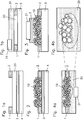
- Fig. 1 a) and b) are electronic components known in the art, each comprising a semiconductive or conductive metal oxide.
- a conductive metal oxide in the form of a thin oxide film 20 was deposited on a dielectric layer 3 acting as a gate and deposited on a conductive electrode 4 of highly doped silicon or metal.
- the electrodes 1, 2 for source and drain are applied directly to the oxide film 20 .
- the electrical conductivity of the oxide film 20 is varied.
- the dielectric layer 3 of Fig. 1a which acts as a gate, is replaced by a solid or liquid electrolyte 30 . Therefore, instead of the conductive electrode 4 (gate electrode), this component has a control electrode 31 which has to have a large surface area in order to be able to make charges available to the electrolyte 30 as quickly as possible.
- the electrodes 1, 2 for source and drain are directly connected to the oxide film 20 in connection.
- the component is located on an electrically non-conductive substrate 5.
- the Fig. 2 to 4 show three embodiments of electronic components according to the invention, the active layer each of a nanocrystalline oxide layer 10 of a semiconducting or conductive Metal oxide exists.
- Fig. 2 an electronic component according to the invention is shown.
- the electrodes 1, 2 for source and drain are in direct contact with the nanocrystalline oxide layer 10.
- the electrical conductivity of the nanocrystalline layer 10 is varied.
- Fig. 3 shows a further embodiment of an electronic component according to the invention.
- the electrically conductive nanocrystalline oxide layer 10 is located on an electrically non-conductive substrate 5 and in direct contact with the electrodes 1, 2 for the source and drain.
- the dielectric layer 3, which functions as the gate was applied as a dispersion to the surface of the nanocrystalline layer 10 , and therefore conforms conformably to the rough surface of the nanocrystalline layer 10 . This ensures that the underlying effect is maximized even on rough surfaces.
- the dielectric layer 3 is in direct contact with a gate electrode 31.
- Fig. 4a shows a particularly advantageous embodiment of a device according to the invention.
- an electrically conductive nanocrystalline oxide layer 10 is in direct contact with the electrodes 1, 2 for the source and drain and the dielectric layer 3 Fig. 2 Which functions as a gate, is replaced with a solid or liquid electrolyte 30th
- the electrolyte 30 is in direct contact with a control electrode 31.
- the control electrode 31 must have a high surface area.
- the change in the conductivity of the nanocrystalline oxide layer 10 is caused by a small voltage between the control electrode 31 and the nanocrystalline layer 10 between the electrodes 1, 2 for source and drain.
- positive charges are generated on the surfaces of the oxide particles. These charges are responsible for the change in the conductivity of the nanocrystalline oxide layer 10.
- the structure described by way of example can be produced by producing a nanoparticulate film 10 between the two electrodes 1, 2, which act as source and drain, by a printing process, in particular by screen printing or inkjet, then sintered to form the conductive bridges between the individual nanoparticles to produce, and is then infiltrated with a solid or liquid electrolyte 30th By applying a control voltage between the electrodes 1, 2 for the source and drain and the control electrode 31 , the element can then be switched.
- the nanoparticles are dispersed directly in an electrolyte, which is liquid at the time of dispersing and printing and later either hardens or remains liquid, and then applied to a substrate in one step by a printing process.
- an electrolyte which is liquid at the time of dispersing and printing and later either hardens or remains liquid
- conductive contacts are produced between the nanoparticles of the conductive oxide and the device according to the invention is functional immediately or after only moderate temperature treatment. This type of production is particularly suitable for use in printable electronics.
- Fig. 5 shows the electrical resistance of two different components according to the invention as a function of time with variation of the control voltage applied between the control electrode 31 and the electrically conductive nanocrystalline layer 10 as electrode between -0.3 V and + 0.8 V ( Fig. 5a )) or between -0.25 V and + 0.85 V ( Fig. 5b )), each at a speed of 0.5 mV / s (Scan) were varied. Both components had an embodiment according to Fig. 4 on.
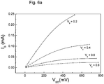
- Fig. 6a shows the current-voltage characteristic of a device according to the invention and proves that this can be operated as a transistor.
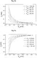
- Fig. 6b) and Fig. 6c show the source characteristic and the drain characteristic of a device according to the invention. The comparison of these two characteristics confirms that the in Fig. 5 shown effects do not go back to leakage currents between the electrodes 1, 2 .
Landscapes
- Engineering & Computer Science (AREA)
- Chemical & Material Sciences (AREA)
- Nanotechnology (AREA)
- Physics & Mathematics (AREA)
- Mathematical Physics (AREA)
- Theoretical Computer Science (AREA)
- Crystallography & Structural Chemistry (AREA)
- Thin Film Transistor (AREA)
Description
- Die Erfindung betrifft ein elektronisches Bauelement mit einer Schicht aus Nanopartikeln, ein Verfahren zu seiner Herstellung und seine Verwendung.
- Die Durchstimmbarkeit von strukturellen und funktionellen Eigenschaften wurde in den vergangenen Jahren für metallische Nanostrukturen in Form von dünnen Filmen und nanoporösen Strukturen, d.h. in Strukturen mit extrem großem Oberflächen-zu-Volumen-Verhältnis, nachgewiesen.
- Die grundlegende Idee der Durchstimmbarkeit der elektronischen Struktur und der Eigenschaften von nanokristallinen Materialien stammt von H. Gleiter, J. Weissmüller, O. Wollersheim und R. Würschum, die sie zuerst in Nanocrystalline Materials: A way to solids with tunable electronic structures and properties?, Acta Mater. 49 (2001), 737-745, veröffentlichten.
- Aus der
DE 199 52 447 C1 und aus J. Weissmüller, R. N. Viswanath, D. Kramer, P. Zimmer, R. Würschum und H. Gleiter, Charge-Induced Reversible Strain in a Metal, Science 300 (2003), 312-315, ist bekannt, dass reversible Längenänderungen von nanoporösem Gold durch das Aufbringen von elektrischen Ladungen an der Grenzfläche eines Elektrolyten zu den metallischen Nanostrukturen in einer Doppelschicht möglich werden. - C. Bansal, S. Sarkar, A.K. Mishra, T. Abraham, C. Lemier und H. Hahn zeigten in Electronically tunable conductivity of a nanoporous Au-Fe alloy, Scripta Materialia 56 (2007), 705-708, dass reversible Änderungen des elektrischen Widerstands von nanoporösem Gold bzw. von nanoporösen Au-Fe-Legierungen durch das Aufbringen von elektrischen Ladungen an der Grenzfläche eines Elektrolyten zu den metallischen Nanostrukturen in einer Doppelschicht möglich werden. Hierbei wurden Änderungen des elektrischen Widerstands im Bereich von einigen Prozent bei angelegten Ladungsdichten von etwa 50 µC/cm2 beobachtet.
- Derselbe Effekt in derselben Größenordnung wurde von M. Sagmeister, U. Brossmann, S. Landgraf, and R. Würschum, in Electrically Tunable Resistance of a Metal, Phys. Rev. Lett. 96 (2006), 156601 für nanoporöses Pt nachgewiesen.
-
US 2006/118853 A1 (TAKATA MASAAKI [JP] ET AL) 8. Juni 2006 beschreibt ein elektronisches Bauelement mit Nanopartikeln - Das Konzept der Durchstimmbarkeit der elektrischen Leitfähigkeit ist bei Halbleitern wie z.B. Si und Ge als so genanntes electric field gating seit Jahrzehnten etabliert und bildet die Basis ihrer Anwendung in der Elektronik. Die grundlegende Struktur besteht hierbei in einer Anordnung aus Source und Drain, die über das halbleitende Material miteinander verbunden sind, sowie einer Gate-Elektrode, die über ein geeignetes Gate-Oxid vom Halbleiter getrennt ist. Die Leitfähigkeit der halbleitenden Schicht wird mittels einer an das Gate angelegten Gate-Spannung über einen weiten Bereich variiert.
Bei Oxiden ist die durch Grenzflächenladungen zu beeinflussbare Zone, die Raumladungszone, sehr viel größer als bei den oben genannten Metallen, aber im Vergleich zu Halbleitern, deren Ladungsträgerdichte geringer ist als die der leitfähigen Oxide, ist die Raumladungszone kleiner. Dennoch gibt es bisher kaum Untersuchungen zur Nutzung von Oxiden als durchstimmbare Materialien.
Im Bereich der funktionellen Eigenschaften von leitenden Oxiden konnten R. Misra, M. McCarthy, und A. F. Hebard in Electric field gating with ionic liquids, Applied Physics Letters 90, (2007) 052905, die elektrische Leitfähigkeit einer dünnen Indiumoxid-Schicht in einer ionischen Flüssigkeit steuern und Änderungen der Sheet-Impedance von mehr als 4 Größenordnungen messen.
Ausgehend hiervon ist es die Aufgabe der vorliegenden Erfindung, ein elektronisches Bauelement, ein Verfahren zu seiner Herstellung und seine Verwendung vorzuschlagen, die die vorher genannten Nachteile und Einschränkungen nicht aufweisen. - Insbesondere soll ein elektronisches Bauelement bereitgestellt werden, das die reversible Durchstimmbarkeit des elektrischen Widerstands in einer Vielzahl von nanoporösen Strukturen mittels einer hieran angelegten Gate-Spannung über viele Größenordnungen ermöglicht.
Diese Aufgabe wird im Hinblick auf das Element durch die Merkmale des Anspruchs 1, im Hinblick auf das Verfahren durch die Verfahrensschritte des Anspruchs 6 oder 7 und im Hinblick auf die Verwendung durch den Anspruch 10 gelöst. Die Unteransprüche beschreiben jeweils vorteilhafte Ausgestaltungen der Erfindung.
Ein erfindungsgemäßes elektronisches Bauelement enthält zunächst zwei Elektroden, die als Source und Drain für das Bauelement fungieren. Zwischen diesen beiden Elektroden befindet sich eine Schicht aus Nanopartikeln, wobei die Nanopartikeln aus einer elektrisch leitenden oder halbleitenden Verbindung eines Metalls mit einem Element aus der VI. Hauptgruppe des Periodensystems der chemischen Elemente, bevorzugt einem Oxid, einem Sulfid oder einem Selenid bestehen.
Hierbei ist entscheidend, dass die Dimensionen der überwiegenden Anzahl der Nanopartikeln zwischen dem 0,1-fachen und dem 10-fachen der Abschirmlänge der elektrisch leitfähigen Verbindung liegen.
Ein erfindungsgemäßes elektronisches Bauelement enthält weiterhin ein Dielektrikum, das zumindest mit einem Teil der Nanopartikel aus der Schicht über mindestens eine gemeinsame Grenzfläche verfügt.
Die Nanopartikel innerhalb der Schicht weisen bevorzugt Partikelgrößen im Bereich von 5 nm bis zu 500 nm auf. Zwischen den Nanopartikeln innerhalb der Schicht befinden sich Poren, die bevorzugt eine Porengrößenverteilung im Bereich von 5 nm bis zu 500 nm aufweisen. - Die Nanopartikel bestehen vorzugsweise aus einem elektrisch leitfähigen Metalloxid, Metallsulfid oder Metallselenid. Besonders bevorzugt sind hierbei transparente leitende Oxide, insbesondere aus Indium-Zinn-Oxid (ITO), aus fluordotiertem Zinn(IV)oxid (SnO2: F; FTO), aus antimondotiertem Zinn(IV)oxid (SnO2:Sb, ATO) oder aus aluminiumdotiertem Zinkoxid (AZO). Insbesondere bei erhöhten Temperaturen eignen sich Nanopartikel aus Zinkoxid, Titandioxid, Zinksulfid oder Cadmiumsulfid.
- In einer besonderen Ausgestaltung liegen die Nanopartikel als gesinterte nanoporöse Volumenstrukturen vor, die bei moderaten Temperaturen gesintert wurden. Die Porenstruktur weist ausgeprägte Korngrenzen/Grenzflächen zwischen den Partikeln oder Körnern der anorganischen Phase auf.
- In einer weiteren Ausgestaltung liegen die Nanopartikel in Form von locker zusammenhängenden porösen Strukturen vor, die nur wenig ausgeprägte Grenzflächen zwischen sich berührenden Partikeln der anorganischen Phase besitzen.
- In einer bevorzugten Ausgestaltung enthält das erfindungsgemäße elektronische Bauelement eine Schicht aus Nanopartikeln, die in Form einer planaren Struktur auf das Dielektrikum aufgebracht ist. Das Dielektrikum selbst liegt in Form einer planaren dielektrischen Schicht vor, die ihrerseits auf einer planaren elektrisch leitfähigen Schicht aufgebracht ist. Zwischen der dünnen Schicht aus Nanopartikeln der leitenden oder halbleitenden Verbindung und einem geeigneten Elektrolyten bilden sich daher ebene Grenzflächen zwischen der Verbindung und dem Dielektrium aus.
- In einer weiteren Ausgestaltung enthält das erfindungsgemäße elektronische Bauelement eine Schicht aus Nanopartikeln, die auf ein elektrisch isolierendes Substrat aufgebracht ist. Das Dielektrikum befindet sich auf der Oberfläche der Schicht aus Nanopartikeln und steht in direktem Kontakt mit einer Steuerelektrode. Vorzugsweise wurde das Dielektrikum (Gate-Dielektrik-Schicht) als Dispersion aufgebracht und liegt daher konform an die raue Oberfläche der Funktionsschicht an. Damit ist sichergestellt, dass der erfindungsgemäße Effekt auch bei rauen Oberflächen maximal wird.
- In einer besonders bevorzugten Ausgestaltung enthält das erfindungsgemäße elektronische Bauelement ein bi-kontinuierliches, interpenetrierendes Komposit-Netzwerk, das aus halbleitenden oder leitenden Nanopartikeln und einem geeigneten Elektrolyten als Dielektrikum besteht und eine Anordnung aus komplex geformten zufälligen Grenzflächen zwischen dem Elektrolyten und den einzelnen Nanopartikeln ausbildet. Auch hier befindet sich das Dielektrikum in Kontakt mit einer Steuerelektrode. Der Elektrolyt selbst kann in einer flüssigen oder in einer festen Phase vorliegen.
- An der Grenzfläche zwischen Elektrolyt und den Nanopartikeln lassen sich elektrische Ladungen durch Anlegen eines Potentials aufbringen. Die elektrischen Ladungen werden durch Änderung des Potentials reversibel variiert, wodurch sich die elektrische Leitfähigkeit der Schicht aus Nanopartikeln reversibel verändern lässt. Alle Oberflächen der Nanopartikel befinden sich in direktem Kontakt zum Elektrolyten und können damit alle Oberflächen mit Ladungen belegen. Auf diese Weise wird ein besonders hoher Effekt erzielt, der eine Durchstimmbarkeit der Schicht über mehrere Größenordnungen ermöglicht. Die Strukturdimensionen der Nanopartikel müssen dabei in der Größenordnung der Abschirmlänge liegen, damit sich die elektrische Leitfähigkeit der Oxidphase merklich variieren lässt.
- Um die Kapazitäten des vorliegenden elektronischen Bauelements zu optimieren, sollten, wie auch in Bauelementen erforderlich, nur kleine Flächen verwendet werden. Auf diese Weise lassen sich die Schaltzeiten des Bauelements möglichst kurz halten.
- Zum Betrieb eines erfindungsgemäßen elektronischen Bauelements wird ein Potential zwischen der Schicht aus Nanopartikeln und einer Gegenelektrode angelegt. Diese Anordnung wurde bereits als funktionsfähige Einheit realisiert und die reversible Änderung der elektrischen Leitfähigkeit ließ sich über mehrere Größenordnungen nachweisen.
- Die Strukturen eines erfindungsgemäßen elektronischen Bauelements können durch konventionelle Schichtpräparationsverfahren synthetisiert werden und anschließend mit einem flüssigen oder festen Elektrolyten (Dielektrikum) belegt werden.
- Als Schichtpräparationsverfahren kommen insbesondere die folgenden Verfahren in Frage:
- (1) Sputtern oder Vakuum-Aufdampfverfahren;
- (2) Spin-Coating oder Druckverfahren, bevorzugt Siebdruckverfahren oder Ink-Jet-Drucken, von Dispersionen der anorganischen Nanopartikel mit anschließendem Sinterschritt;
- (3) Spin-Coating oder Druckverfahren, bevorzugt Siebdruckverfahren oder Ink-Jet-Drucken, von Dispersionen der anorganischen Nanopartikel mit Elektrolyt mit einem anschließenden Temperschritt.
- In den Verfahren (1) und (2) wird der flüssige oder feste Elektrolyt nach der Schichtherstellung und einem ggf. erforderlichen Sinter- oder Temperschritt als weitere Schicht auf die dünne Schicht der anorganischen Phase aufgebracht und anschließend mit einer Elektrode mit großer Oberfläche versehen.
- In Verfahren (3) werden die Nanopartikel der anorganischen Phase direkt in einem flüssigen Elektrolyten dispergiert und auf ein geeignetes Substrat durch Spin-Coating oder ein Druckverfahren, bevorzugt Siebdruckverfahren oder Ink-Jet-Drucken, aufgebracht. Ein Temperschritt, der mit den eingesetzten Substraten, dem gewählten Druckverfahren und dem Elektrolyten verträglich ist, kann zum Erzeugen einer optimalen elektrischen Leitfähigkeit über die Grenzflächen der anorganischen Phase angeschlossen werden.
- An Stelle eines flüssigen Elektrolyten kann auch ein Elektrolyt verwendet werden, der vor seiner Trocknung flüssig ist und durch Trocknung fest wird. Bei Einsatz eines derartigen Elektrolyten, der durch Trocknung fest wird, kann die Schrumpfung der Elektrolytphase dazu dienen, um die anorganischen Nanopartikel zusammenzuziehen und auf diese Weise eine höhere elektrische Leitfähigkeit zu erhalten.
- Erfindungsgemäße elektronische Bauelemente lassen sich insbesondere als Dioden, Transistoren, Spannungsinverter oder als Sensoren verwenden.
- Der Einsatz von nanokristallinen funktionellen Partikeln aus einer Verbindung eines Metalls mit einem Element aus der VI. Hauptgruppe des Periodensystems, d.h. insbesondere Oxide, Sulfide und Selenide, in Kombination mit der Nutzung der Durchstimmbarkeit von Materialeigenschaften durch reversible Aufladung in einem Elektrolyten führt zu neuen Möglichkeiten für funktionelle Bauelemente im Bereich der druckbaren Elektronik. Besonders vorteilhaft für die druckbare Elektronik ist der Einsatz eines druckfähigen Elektrolyt-Nanopartikel-Gemischs.
- Die Erfindung wird im Folgenden anhand von Ausführungsbeispielen und den Figuren näher erläutert. Hierbei zeigen
- Fig. 1
- Elektronische Bauelemente mit einem leitfähigen Oxid (Stand der Technik) a) ohne bzw. b) mit Elektrolyt.
- Fig. 2
- Erfindungsgemäßes elektronisches Bauelement mit einer Schicht aus Nanopartikeln in Form einer planaren Struktur auf einem Dielektrikum, das in Form einer planaren dielektrischen Schicht vorliegt.
- Fig. 3
- Erfindungsgemäßes elektronisches Bauelement, bei dem sich das Dielektrikum auf der Oberfläche der Schicht aus Nanopartikeln befindet.
- Fig. 4
- Erfindungsgemäßes elektronisches Bauelement, bei dem das Dielektrikum in Form eines Elektrolyten vorliegt, der mit den Nanopartikeln der Schicht ein interpenetrierendes Netzwerk ausbildet.
- Fig. 5
- Änderung des elektrischen Widerstands zweier erfindungsgemäßer elektronischer Bauelemente mit der Zeit bei Variation der Gate-Spannung.
- Fig. 6
- a) Strom-Spannungs-Charakteristik, b) Source-Charakteristik und c) Drain-Charakteristik eines erfindungsgemäßen elektronischen Bauelements.
- In
Fig. 1 a) und b) sind elektronische Bauelemente dargestellt, die aus dem Stand der Technik bekannt sind und die jeweils ein halbleitendes oder leitendes Metalloxid umfassen. - In dem in
Fig. 1a ) dargestellten elektronischen Bauelement wurde ein leitfähiges Metalloxid in Form eines dünnen Oxidfilms 20 auf einer dielektrischen Schicht 3, die als Gate fungiert und die auf einer leitfähigen Elektrode 4 aus hoch dotiertem Silizium oder Metall aufgebracht ist, abgeschieden. Die Elektroden 1, 2 für Source und Drain sind direkt auf dem Oxidfilm 20 aufgebracht. Durch Anlegen einer Gate-Spannung an die dielektrische Schicht 3 wird die elektrische Leitfähigkeit des Oxidfilms 20 variiert. - In dem in
Fig. 1b ) dargestellten elektronischen Bauelement ist die dielektrische Schicht 3 ausFig. 1a ), die als Gate fungiert, durch einen festen oder flüssigen Elektrolyten 30 ersetzt. Daher weist dieses Bauelement an Stelle der leitfähigen Elektrode 4 (Gate-Elektrode) eine Steuerelektrode 31 auf, die eine große Oberfläche besitzen muss, um dem Elektrolyten 30 möglichst schnell Ladungen zur Verfügung stellen zu können. Auch hier stehen die Elektroden 1, 2 für Source und Drain direkt mit dem Oxidfilm 20 in Verbindung. Das Bauelement befindet sich auf einem elektrisch nicht leitfähigen Substrat 5. - Die
Fig. 2 bis 4 zeigen drei Ausgestaltungen von erfindungsgemäßen elektronischen Bauelementen, deren aktive Schicht jeweils aus einer nanokristallinen Oxidschicht 10 aus einem halbleitenden oder leitenden Metalloxid besteht. - In
Fig. 2 ist ein erfindungsgemäßes elektronisches Bauelement dargestellt. Hierbei wurde eine elektrisch leitfähige nanokristalline Oxidschicht 10 auf einer dielektrischen Schicht 3, die als Gate fungiert und die sich auf einer leitfähigen Elektrode 4 aus hoch dotiertem Silizium oder Metall befindet, durch ein Druckverfahren mit oder ohne anschließenden Sinterschritt aufgebracht. Die Elektroden 1, 2 für Source und Drain stehen sich in direktem Kontakt mit der nanokristallinen Oxidschicht 10. Durch Anlegen einer Gate-Spannung an die dielektrische Schicht 3 wird die elektrische Leitfähigkeit der nanokristallinen Schicht 10 variiert. -
Fig. 3 zeigt eine weitere Ausgestaltung eines erfindungsgemäßen elektronischen Bauelements. Hierbei befindet sich die elektrisch leitfähige nanokristalline Oxidschicht 10 auf einem elektrisch nicht leitfähigen Substrat 5 sowie in direktem Kontakt mit den Elektroden 1, 2 für Source und Drain. Die dielektrische Schicht 3, die das Gate fungiert, wurde jedoch als Dispersion auf die Oberfläche der nanokristallinen Schicht 10 aufgebracht und liegt deshalb konform an der rauen Oberfläche der nanokristallinen Schicht 10 an. Damit ist sichergestellt, dass der zugrunde liegende Effekt auch bei rauen Oberflächen maximal wird. Die dielektrische Schicht 3 befindet sich im direkten Kontakt mit einer Gate-Elektrode 31. -
Fig. 4a ) zeigt eine besonders vorteilhafte Ausgestaltung eines erfindungsgemäßen Bauelements. Hierbei befindet sich eine elektrisch leitfähige nanokristalline Oxidschicht 10 im direkten Kontakt mit den Elektroden 1, 2 für Source und Drain und die dielektrische Schicht 3 ausFig. 2 , die als Gate fungiert, ist durch einen festen oder flüssigen Elektrolyten 30 ersetzt. Der Elektrolyt 30 steht in direktem Kontakt mit einer Steuerelektrode 31. Auch in dieser Ausgestaltung muss die Steuerelektrode 31 eine hohe Oberfläche besitzen. - Die Änderung der Leitfähigkeit der nanokristallinen Oxidschicht 10 wird durch eine kleine Spannung zwischen der Steuerelektrode 31 und der nanokristallinen Schicht 10 zwischen den Elektroden 1, 2 für Source und Drain bewirkt. Wie in der Vergrößerung in
Fig. 4b ) für ein Beispiel mit positiven Ladungen dargestellt, werden an den Oberflächen der Oxidpartikel positive Ladungen erzeugt. Diese Ladungen sind für die Veränderung der Leitfähigkeit der nanokristallinen Oxidschicht 10 verantwortlich. - Die in
Fig. 4 beispielhaft beschriebene Struktur kann hergestellt werden, indem zwischen den beiden Elektroden 1, 2, die als Source und Drain fungieren, ein nanopartikulärer Film 10 durch ein Druckverfahren, insbesondere mittels Siebdruck oder Inkjet, hergestellt, anschließend gesintert, um die leitfähigen Brücken zwischen den einzelnen Nanopartikeln zu erzeugen, und dann mit einem festen oder flüssigen Elektrolyten 30 infiltriert wird. Durch das Anlegen einer Steuerspannung zwischen den Elektroden 1, 2 für Source und Drain sowie der Steuerelektrode 31 lässt sich dann das Element schalten. - In einer alternativen Ausgestaltung werden die Nanopartikel direkt in einem Elektrolyten, der zum Zeitpunkt des Dispergierens und Druckens flüssig ist und später entweder aushärtet oder flüssig bleibt, dispergiert und anschließend in einem Schritt durch ein Druckverfahren auf ein Substrat aufgebracht. Während des Druck- und Trocknungsvorgangs werden leitfähige Kontakte zwischen den Nanopartikeln des leitfähigen Oxids erzeugt und das erfindungsgemäße Bauelement ist sofort oder nach nur moderater Temperaturbehandlung funktionsfähig. Diese Art der Herstellung eignet sich insbesondere für den Einsatz in der druckbaren Elektronik.
-
Fig. 5 zeigt den elektrischen Widerstand von zwei verschiedenen erfindungsgemäßen Bauelementen als Funktion der Zeit bei Variation der zwischen der Steuerelektrode 31 und der elektrisch leitfähigen nanokristallinen Schicht 10 als Elektrode angelegten Steuerspannung zwischen -0,3 V und + 0,8 V (Fig. 5a )) bzw. zwischen -0,25 V und + 0,85 V (Fig. 5b )), die jeweils mit einer Geschwindigkeit von 0,5 mV/s (Scan) variiert wurden. Beide Bauelemente wiesen eine Ausgestaltung gemäßFig. 4 auf. Diesen Messergebnissen ist zu entnehmen, dass sich der elektrische Widerstand der beiden Bauelemente durch einfache Variation der Steuerspannung um einen Faktor 350 (= 35 000%;Fig. 5a ) bzw. 100 (= 10 000%;Fig. 5b ) verändern lässt. Dieser Effekt liegt damit um mehrere Größenordnungen über den in C. Bansal et al., Scripta Materialia 56 (2007), 705 ff, beschriebenen reversiblen Änderungen des elektrischen Widerstands von nanoporösem Gold bzw. von nanoporösen Au-Fe-Legierungen. -
Fig. 6a ) zeigt die Strom-Spannungs-Charakteristik eines erfindungsgemäßen Bauelements und belegt, dass sich dieses als Transistor betreiben lässt. -
Fig. 6b) und Fig. 6c ) zeigen die Source-Charakteristik bzw. die Drain-Charakteristik eines erfindungsgemäßen Bauelements. Der Vergleich dieser beiden Charakteristiken bestätigt, dass die inFig. 5 gezeigten Effekte nicht auf Leckströme zwischen den Elektroden 1, 2 zurückgehen.
Claims (10)
- Elektronisches Bauelement, umfassend
zwei Elektroden (1,2), zwischen denen sich eine Schicht (10) aus Nanopartikeln, die aus einer elektrisch leitfähigen Verbindung eines Metalls mit einem Element aus der VI. Hauptgruppe des Periodensystems bestehen, befindet, wobei die Dimensionen der überwiegenden Anzahl der Nanopartikel zwischen dem 0,1-fachen und dem 10-fachen der Abschirmlänge der elektrisch leitfähigen Verbindung liegen, und ein Dielektrikum, das zumindest mit einem Teil der Nanopartikel aus der Schicht (10) mindestens eine gemeinsame Grenzfläche ausbildet, dadurch gekennzeichnet,
dass die Schicht (10) durch einen gedruckten nanopartikulären Film gebildet wird, das Dielektrikum in Form eines festen oder flüssigen Elektrolyten (30) vorliegt, der mit den Nanopartikeln der Schicht (10) ein interpenetrierendes Netzwerk ausbildet und in Kontakt mit einer Steuerelektrode (31) steht. - Elektronisches Bauelement mit einer Schicht (10) aus Nanopartikeln nach Anspruch 1, wobei die Nanopartikel Partikelgrößen von 5 nm bis zu 500 nm aufweisen und sich zwischen den Nanopartikeln in der Schicht (10) Poren befinden, die eine Porengrößenverteilung von 5 nm bis zu 500 nm aufweisen.
- Elektronisches Bauelement nach Anspruch 1 oder 2 mit Nanopartikeln aus einem elektrisch leitfähigen Metalloxid, Metallsulfid oder Metallselenid.
- Elektronisches Bauelement nach Anspruch 3 mit Nanopartikeln aus Indium-Zinnoxid, fluor- oder antimondotiertem Zinn(IV)-oxid oder aluminiumdotiertem Zinkoxid.
- Elektronisches Bauelement nach Anspruch 3 mit Nanopartikeln aus Zinkoxid, Titandioxid, Zinksulfid oder Cadmiumsulfid.
- Verfahren zur Herstellung eines elektronischen Bauelements nach einem der Ansprüche 1 bis 5, bei dem die Strukturen eines erfindungsgemäßen elektronischen Bauelements durch ein Druckverfahren mit einem anschließenden Sinterschritt oder Temperschritt hergestellt werden.
- Verfahren zur Herstellung eines elektronischen Bauelements nach einem der Ansprüche 1 bis 5, bei dem die Strukturen eines erfindungsgemäßen elektronischen Bauelements durch ein Druckverfahren mit einem anschließenden Sinterschritt oder Temperschritt hergestellt und hieran anschließend mit einem Elektrolyten belegt werden.
- Verfahren nach Anspruch 7, wobei die Nanopartikel direkt in einen flüssigen Elektrolyten dispergiert und hieran anschließend durch Spin-Coating oder mittels eines Druckverfahrens auf ein Substrat aufgebracht werden.
- Verfahren nach einem der Ansprüche 7 oder 8, wobei ein flüssiger Elektrolyt eingesetzt wird, der, nachdem er auf das Substrat aufgebracht wurde, fest wird.
- Verwendung eines elektronischen Bauelements nach einem der Ansprüche 1 bis 5 als Diode, Transistor, Spannungsinverter oder Sensor.
Applications Claiming Priority (2)
| Application Number | Priority Date | Filing Date | Title |
|---|---|---|---|
| DE102007043360A DE102007043360A1 (de) | 2007-09-12 | 2007-09-12 | Elektronisches Bauelement, Verfahren zu seiner Herstellung und seine Verwendung |
| PCT/EP2008/006818 WO2009036856A1 (de) | 2007-09-12 | 2008-08-20 | Elektronisches bauelement, verfahren zu seiner herstellung und seine verwendung |
Publications (2)
| Publication Number | Publication Date |
|---|---|
| EP2188841A1 EP2188841A1 (de) | 2010-05-26 |
| EP2188841B1 true EP2188841B1 (de) | 2018-10-10 |
Family
ID=39865672
Family Applications (1)
| Application Number | Title | Priority Date | Filing Date |
|---|---|---|---|
| EP08785631.6A Not-in-force EP2188841B1 (de) | 2007-09-12 | 2008-08-20 | Elektronisches bauelement, verfahren zu seiner herstellung und seine verwendung |
Country Status (5)
| Country | Link |
|---|---|
| US (1) | US8558214B2 (de) |
| EP (1) | EP2188841B1 (de) |
| JP (1) | JP5479344B2 (de) |
| DE (1) | DE102007043360A1 (de) |
| WO (1) | WO2009036856A1 (de) |
Families Citing this family (7)
| Publication number | Priority date | Publication date | Assignee | Title |
|---|---|---|---|---|
| EP2654074B1 (de) | 2010-03-31 | 2016-10-26 | EV Group E. Thallner GmbH | Verfahren zum permanenten Verbinden zweier Metalloberflächen |
| EP2423965A1 (de) | 2010-08-27 | 2012-02-29 | Karlsruher Institut für Technologie | Elektrochemischer Transistor und Verfahren zu dessen Herstellung |
| EP2629356B1 (de) | 2012-02-17 | 2016-02-17 | Karlsruher Institut für Technologie | Gedruckte Elektronik hergestellt durch Abscheiden eines festen Verbundpolymerelektrolyts und Verwendung eines festen Verbundpolymerelektrolyts zum Drucken von Elektronik |
| US8927967B2 (en) * | 2013-04-24 | 2015-01-06 | Karlsruhe Institute Of Technology | Electrochemically-gated field-effect transistor, methods for its manufacture and use thereof |
| US10167193B2 (en) | 2014-09-23 | 2019-01-01 | Vanderbilt University | Ferroelectric agglomerates and methods and uses related thereto |
| US9903016B2 (en) * | 2014-10-23 | 2018-02-27 | E/G Electro-Graph, Inc. | Device having preformed triple junctions to maintain electrode conductivity and a method for making and using the device |
| EP3261128A1 (de) * | 2016-06-23 | 2017-12-27 | Karlsruher Institut für Technologie | Vertikaler feldeffektransistor, verfahren zu seiner herstellung, seiner verwendung und elektronik mit dem feldeffekttransistor |
Family Cites Families (16)
| Publication number | Priority date | Publication date | Assignee | Title |
|---|---|---|---|---|
| US6294401B1 (en) * | 1998-08-19 | 2001-09-25 | Massachusetts Institute Of Technology | Nanoparticle-based electrical, chemical, and mechanical structures and methods of making same |
| DE19952447C1 (de) | 1999-10-30 | 2001-01-18 | Karlsruhe Forschzent | Vorrichtung mit einer Elektrode, einer schwammartigen perkolierenden Schicht, einem Elektrolyten und einem Mittel zum Anlegen einer Spannung |
| DE10059498A1 (de) * | 2000-11-30 | 2002-06-13 | Infineon Technologies Ag | Substrat mit einer halbleitenden Schicht, elektronisches Bauelement mit diesem Substrat, elektronische Schaltung mit mindestens einem solchen elektronischen Bauelement, druckbare Zusammensetzung sowie Verfahren zur Herstellung eines Substrats |
| EP2194026A1 (de) * | 2002-09-30 | 2010-06-09 | Nanosys, Inc. | Nano-bereite grossflächige makroelektronische Substraten und Verwendung davon |
| JP2006509260A (ja) * | 2002-12-09 | 2006-03-16 | ピクセリジェント・テクノロジーズ・エルエルシー | ナノサイズの半導体粒子をベースとするプログラム可能なフォトリソグラフィマスクおよび可逆性フォトブリーチング可能な材料、ならびにそれらの用途 |
| US20110294296A1 (en) * | 2003-05-21 | 2011-12-01 | Lucent Technologies Inc. | Using edges of self-assembled monolayers to form narrow features |
| WO2005036599A2 (en) * | 2003-10-06 | 2005-04-21 | Massachusetts Institute Of Technology | Non-volatile memory device |
| WO2005089165A2 (en) * | 2004-03-10 | 2005-09-29 | Nanosys, Inc. | Nano-enabled memory devices and anisotropic charge carrying arrays |
| US7742322B2 (en) * | 2005-01-07 | 2010-06-22 | Invisage Technologies, Inc. | Electronic and optoelectronic devices with quantum dot films |
| US7355238B2 (en) * | 2004-12-06 | 2008-04-08 | Asahi Glass Company, Limited | Nonvolatile semiconductor memory device having nanoparticles for charge retention |
| JP2006227254A (ja) * | 2005-02-17 | 2006-08-31 | Konica Minolta Holdings Inc | 電気化学トランジスタ、及びこれを用いた表示素子 |
| JP2006227488A (ja) * | 2005-02-21 | 2006-08-31 | Konica Minolta Holdings Inc | 表示素子 |
| US7691666B2 (en) * | 2005-06-16 | 2010-04-06 | Eastman Kodak Company | Methods of making thin film transistors comprising zinc-oxide-based semiconductor materials and transistors made thereby |
| US7507618B2 (en) * | 2005-06-27 | 2009-03-24 | 3M Innovative Properties Company | Method for making electronic devices using metal oxide nanoparticles |
| US7575978B2 (en) * | 2005-08-04 | 2009-08-18 | Micron Technology, Inc. | Method for making conductive nanoparticle charge storage element |
| JP2007073969A (ja) * | 2005-09-07 | 2007-03-22 | Samsung Electronics Co Ltd | 電荷トラップ型メモリ素子及びその製造方法 |
-
2007
- 2007-09-12 DE DE102007043360A patent/DE102007043360A1/de not_active Withdrawn
-
2008
- 2008-08-20 WO PCT/EP2008/006818 patent/WO2009036856A1/de not_active Ceased
- 2008-08-20 EP EP08785631.6A patent/EP2188841B1/de not_active Not-in-force
- 2008-08-20 JP JP2010524371A patent/JP5479344B2/ja not_active Expired - Fee Related
- 2008-08-20 US US12/677,848 patent/US8558214B2/en not_active Expired - Fee Related
Non-Patent Citations (1)
| Title |
|---|
| None * |
Also Published As
| Publication number | Publication date |
|---|---|
| US20100308299A1 (en) | 2010-12-09 |
| JP2010539688A (ja) | 2010-12-16 |
| WO2009036856A1 (de) | 2009-03-26 |
| DE102007043360A1 (de) | 2009-03-19 |
| EP2188841A1 (de) | 2010-05-26 |
| JP5479344B2 (ja) | 2014-04-23 |
| US8558214B2 (en) | 2013-10-15 |
Similar Documents
| Publication | Publication Date | Title |
|---|---|---|
| DE602004001508T2 (de) | Elektrochromische anzeigeeinrichtung | |
| DE69132469T2 (de) | Elektrische Anordnung mit einem dotierten amorphen Siliziumkanal | |
| DE69032893T2 (de) | Werkstoff für elektrische Leiter, Elektronikagerät welches diesen verwendet und Flüssig-Kristall-Anzeige | |
| EP2188841A1 (de) | Elektronisches bauelement, verfahren zu seiner herstellung und seine verwendung | |
| EP3391135B1 (de) | Elektrisch schaltbare verglasung umfassend flächenelektroden mit anisotroper leitfähigkeit | |
| DE3531443A1 (de) | Optische vorrichtung mit variabler durchlaessigkeit oder variabler durchlassung von strahlen | |
| DE102018213062B3 (de) | Integrierter elektronischer Schaltkreis mit einem ersten Transistor und einem ferroelektrischen Kondensator und Verfahren zu seiner Herstellung | |
| DE60000985T2 (de) | Elektronische anzeige | |
| EP1224676B1 (de) | Aktor mit einer elektrode, einer schwammartigen perkolierenden schicht, einem elektrolyten und einem mittel zum anlegen einer spannung | |
| EP1825516A2 (de) | Gatter aus organischen feldeffekttransistoren | |
| EP1656683B1 (de) | Organischer kondensator mit spannungsgesteuerter kapazität | |
| DE69212528T2 (de) | Verfahren zur Herstellung einer Nickeloxid-Elektrode mit eingelagerten Lithiumionen | |
| EP3414769B1 (de) | Mikroelektronische elektrodenanordnung | |
| CH641586A5 (en) | Liquid-crystal display panel in a matrix arrangement | |
| DE2326108A1 (de) | Festkoerper-speicherbauelement | |
| WO2012022312A2 (de) | Solarzellenmodul und herstellungsverfahren hierfür | |
| DE2637481A1 (de) | Duennschicht-transistoreinrichtung | |
| DE102014215492A1 (de) | Sensor zum Erfassen zumindest einer chemischen Spezies und Verfahren zu dessen Herstellung | |
| DE102018130131A1 (de) | Schaltbares Widerstands-Bauelement und Verfahren zu seiner Herstellung | |
| DE102010021344A1 (de) | Elektronisches Bauelement und seine Verwendung | |
| DE102019211970A1 (de) | Verfahren zum Herstellen eines gedruckten magnetischen Funktionselements und gedrucktes magnetisches Funktionselement | |
| DE102004057236B4 (de) | Nicht-flüchtiges resistives Speicherelement | |
| DE102022116981A1 (de) | Memristive struktur und memristive vorrichtung | |
| DE19546962A1 (de) | Metallisierungsstruktur und Flüssigkristallvorrichtung | |
| EP1911089A1 (de) | Elektronisches bauelement |
Legal Events
| Date | Code | Title | Description |
|---|---|---|---|
| PUAI | Public reference made under article 153(3) epc to a published international application that has entered the european phase |
Free format text: ORIGINAL CODE: 0009012 |
|
| 17P | Request for examination filed |
Effective date: 20100202 |
|
| AK | Designated contracting states |
Kind code of ref document: A1 Designated state(s): AT BE BG CH CY CZ DE DK EE ES FI FR GB GR HR HU IE IS IT LI LT LU LV MC MT NL NO PL PT RO SE SI SK TR |
|
| AX | Request for extension of the european patent |
Extension state: AL BA MK RS |
|
| DAX | Request for extension of the european patent (deleted) | ||
| 17Q | First examination report despatched |
Effective date: 20111028 |
|
| GRAP | Despatch of communication of intention to grant a patent |
Free format text: ORIGINAL CODE: EPIDOSNIGR1 |
|
| STAA | Information on the status of an ep patent application or granted ep patent |
Free format text: STATUS: GRANT OF PATENT IS INTENDED |
|
| INTG | Intention to grant announced |
Effective date: 20180504 |
|
| GRAS | Grant fee paid |
Free format text: ORIGINAL CODE: EPIDOSNIGR3 |
|
| GRAA | (expected) grant |
Free format text: ORIGINAL CODE: 0009210 |
|
| STAA | Information on the status of an ep patent application or granted ep patent |
Free format text: STATUS: THE PATENT HAS BEEN GRANTED |
|
| AK | Designated contracting states |
Kind code of ref document: B1 Designated state(s): AT BE BG CH CY CZ DE DK EE ES FI FR GB GR HR HU IE IS IT LI LT LU LV MC MT NL NO PL PT RO SE SI SK TR |
|
| REG | Reference to a national code |
Ref country code: GB Ref legal event code: FG4D Free format text: NOT ENGLISH |
|
| REG | Reference to a national code |
Ref country code: CH Ref legal event code: EP Ref country code: AT Ref legal event code: REF Ref document number: 1052238 Country of ref document: AT Kind code of ref document: T Effective date: 20181015 |
|
| REG | Reference to a national code |
Ref country code: IE Ref legal event code: FG4D Free format text: LANGUAGE OF EP DOCUMENT: GERMAN |
|
| REG | Reference to a national code |
Ref country code: DE Ref legal event code: R096 Ref document number: 502008016387 Country of ref document: DE |
|
| REG | Reference to a national code |
Ref country code: NL Ref legal event code: MP Effective date: 20181010 |
|
| REG | Reference to a national code |
Ref country code: LT Ref legal event code: MG4D |
|
| PG25 | Lapsed in a contracting state [announced via postgrant information from national office to epo] |
Ref country code: NL Free format text: LAPSE BECAUSE OF FAILURE TO SUBMIT A TRANSLATION OF THE DESCRIPTION OR TO PAY THE FEE WITHIN THE PRESCRIBED TIME-LIMIT Effective date: 20181010 |
|
| PG25 | Lapsed in a contracting state [announced via postgrant information from national office to epo] |
Ref country code: FI Free format text: LAPSE BECAUSE OF FAILURE TO SUBMIT A TRANSLATION OF THE DESCRIPTION OR TO PAY THE FEE WITHIN THE PRESCRIBED TIME-LIMIT Effective date: 20181010 Ref country code: IS Free format text: LAPSE BECAUSE OF FAILURE TO SUBMIT A TRANSLATION OF THE DESCRIPTION OR TO PAY THE FEE WITHIN THE PRESCRIBED TIME-LIMIT Effective date: 20190210 Ref country code: BG Free format text: LAPSE BECAUSE OF FAILURE TO SUBMIT A TRANSLATION OF THE DESCRIPTION OR TO PAY THE FEE WITHIN THE PRESCRIBED TIME-LIMIT Effective date: 20190110 Ref country code: LT Free format text: LAPSE BECAUSE OF FAILURE TO SUBMIT A TRANSLATION OF THE DESCRIPTION OR TO PAY THE FEE WITHIN THE PRESCRIBED TIME-LIMIT Effective date: 20181010 Ref country code: NO Free format text: LAPSE BECAUSE OF FAILURE TO SUBMIT A TRANSLATION OF THE DESCRIPTION OR TO PAY THE FEE WITHIN THE PRESCRIBED TIME-LIMIT Effective date: 20190110 Ref country code: ES Free format text: LAPSE BECAUSE OF FAILURE TO SUBMIT A TRANSLATION OF THE DESCRIPTION OR TO PAY THE FEE WITHIN THE PRESCRIBED TIME-LIMIT Effective date: 20181010 Ref country code: HR Free format text: LAPSE BECAUSE OF FAILURE TO SUBMIT A TRANSLATION OF THE DESCRIPTION OR TO PAY THE FEE WITHIN THE PRESCRIBED TIME-LIMIT Effective date: 20181010 Ref country code: PL Free format text: LAPSE BECAUSE OF FAILURE TO SUBMIT A TRANSLATION OF THE DESCRIPTION OR TO PAY THE FEE WITHIN THE PRESCRIBED TIME-LIMIT Effective date: 20181010 Ref country code: LV Free format text: LAPSE BECAUSE OF FAILURE TO SUBMIT A TRANSLATION OF THE DESCRIPTION OR TO PAY THE FEE WITHIN THE PRESCRIBED TIME-LIMIT Effective date: 20181010 |
|
| PG25 | Lapsed in a contracting state [announced via postgrant information from national office to epo] |
Ref country code: PT Free format text: LAPSE BECAUSE OF FAILURE TO SUBMIT A TRANSLATION OF THE DESCRIPTION OR TO PAY THE FEE WITHIN THE PRESCRIBED TIME-LIMIT Effective date: 20190210 Ref country code: SE Free format text: LAPSE BECAUSE OF FAILURE TO SUBMIT A TRANSLATION OF THE DESCRIPTION OR TO PAY THE FEE WITHIN THE PRESCRIBED TIME-LIMIT Effective date: 20181010 Ref country code: GR Free format text: LAPSE BECAUSE OF FAILURE TO SUBMIT A TRANSLATION OF THE DESCRIPTION OR TO PAY THE FEE WITHIN THE PRESCRIBED TIME-LIMIT Effective date: 20190111 |
|
| REG | Reference to a national code |
Ref country code: DE Ref legal event code: R097 Ref document number: 502008016387 Country of ref document: DE |
|
| PG25 | Lapsed in a contracting state [announced via postgrant information from national office to epo] |
Ref country code: IT Free format text: LAPSE BECAUSE OF FAILURE TO SUBMIT A TRANSLATION OF THE DESCRIPTION OR TO PAY THE FEE WITHIN THE PRESCRIBED TIME-LIMIT Effective date: 20181010 Ref country code: DK Free format text: LAPSE BECAUSE OF FAILURE TO SUBMIT A TRANSLATION OF THE DESCRIPTION OR TO PAY THE FEE WITHIN THE PRESCRIBED TIME-LIMIT Effective date: 20181010 Ref country code: CZ Free format text: LAPSE BECAUSE OF FAILURE TO SUBMIT A TRANSLATION OF THE DESCRIPTION OR TO PAY THE FEE WITHIN THE PRESCRIBED TIME-LIMIT Effective date: 20181010 |
|
| PLBE | No opposition filed within time limit |
Free format text: ORIGINAL CODE: 0009261 |
|
| STAA | Information on the status of an ep patent application or granted ep patent |
Free format text: STATUS: NO OPPOSITION FILED WITHIN TIME LIMIT |
|
| PG25 | Lapsed in a contracting state [announced via postgrant information from national office to epo] |
Ref country code: EE Free format text: LAPSE BECAUSE OF FAILURE TO SUBMIT A TRANSLATION OF THE DESCRIPTION OR TO PAY THE FEE WITHIN THE PRESCRIBED TIME-LIMIT Effective date: 20181010 Ref country code: RO Free format text: LAPSE BECAUSE OF FAILURE TO SUBMIT A TRANSLATION OF THE DESCRIPTION OR TO PAY THE FEE WITHIN THE PRESCRIBED TIME-LIMIT Effective date: 20181010 Ref country code: SK Free format text: LAPSE BECAUSE OF FAILURE TO SUBMIT A TRANSLATION OF THE DESCRIPTION OR TO PAY THE FEE WITHIN THE PRESCRIBED TIME-LIMIT Effective date: 20181010 |
|
| 26N | No opposition filed |
Effective date: 20190711 |
|
| PG25 | Lapsed in a contracting state [announced via postgrant information from national office to epo] |
Ref country code: SI Free format text: LAPSE BECAUSE OF FAILURE TO SUBMIT A TRANSLATION OF THE DESCRIPTION OR TO PAY THE FEE WITHIN THE PRESCRIBED TIME-LIMIT Effective date: 20181010 |
|
| PG25 | Lapsed in a contracting state [announced via postgrant information from national office to epo] |
Ref country code: TR Free format text: LAPSE BECAUSE OF FAILURE TO SUBMIT A TRANSLATION OF THE DESCRIPTION OR TO PAY THE FEE WITHIN THE PRESCRIBED TIME-LIMIT Effective date: 20181010 |
|
| PG25 | Lapsed in a contracting state [announced via postgrant information from national office to epo] |
Ref country code: LU Free format text: LAPSE BECAUSE OF NON-PAYMENT OF DUE FEES Effective date: 20190820 Ref country code: LI Free format text: LAPSE BECAUSE OF NON-PAYMENT OF DUE FEES Effective date: 20190831 Ref country code: CH Free format text: LAPSE BECAUSE OF NON-PAYMENT OF DUE FEES Effective date: 20190831 Ref country code: MC Free format text: LAPSE BECAUSE OF FAILURE TO SUBMIT A TRANSLATION OF THE DESCRIPTION OR TO PAY THE FEE WITHIN THE PRESCRIBED TIME-LIMIT Effective date: 20181010 |
|
| REG | Reference to a national code |
Ref country code: BE Ref legal event code: MM Effective date: 20190831 |
|
| PG25 | Lapsed in a contracting state [announced via postgrant information from national office to epo] |
Ref country code: IE Free format text: LAPSE BECAUSE OF NON-PAYMENT OF DUE FEES Effective date: 20190820 |
|
| PG25 | Lapsed in a contracting state [announced via postgrant information from national office to epo] |
Ref country code: BE Free format text: LAPSE BECAUSE OF NON-PAYMENT OF DUE FEES Effective date: 20190831 |
|
| REG | Reference to a national code |
Ref country code: AT Ref legal event code: MM01 Ref document number: 1052238 Country of ref document: AT Kind code of ref document: T Effective date: 20190820 |
|
| PG25 | Lapsed in a contracting state [announced via postgrant information from national office to epo] |
Ref country code: AT Free format text: LAPSE BECAUSE OF NON-PAYMENT OF DUE FEES Effective date: 20190820 |
|
| PG25 | Lapsed in a contracting state [announced via postgrant information from national office to epo] |
Ref country code: CY Free format text: LAPSE BECAUSE OF FAILURE TO SUBMIT A TRANSLATION OF THE DESCRIPTION OR TO PAY THE FEE WITHIN THE PRESCRIBED TIME-LIMIT Effective date: 20181010 |
|
| PG25 | Lapsed in a contracting state [announced via postgrant information from national office to epo] |
Ref country code: HU Free format text: LAPSE BECAUSE OF FAILURE TO SUBMIT A TRANSLATION OF THE DESCRIPTION OR TO PAY THE FEE WITHIN THE PRESCRIBED TIME-LIMIT; INVALID AB INITIO Effective date: 20080820 Ref country code: MT Free format text: LAPSE BECAUSE OF FAILURE TO SUBMIT A TRANSLATION OF THE DESCRIPTION OR TO PAY THE FEE WITHIN THE PRESCRIBED TIME-LIMIT Effective date: 20181010 |
|
| PGFP | Annual fee paid to national office [announced via postgrant information from national office to epo] |
Ref country code: GB Payment date: 20220824 Year of fee payment: 15 Ref country code: DE Payment date: 20220822 Year of fee payment: 15 |
|
| PGFP | Annual fee paid to national office [announced via postgrant information from national office to epo] |
Ref country code: FR Payment date: 20220822 Year of fee payment: 15 |
|
| REG | Reference to a national code |
Ref country code: DE Ref legal event code: R119 Ref document number: 502008016387 Country of ref document: DE |
|
| GBPC | Gb: european patent ceased through non-payment of renewal fee |
Effective date: 20230820 |
|
| PG25 | Lapsed in a contracting state [announced via postgrant information from national office to epo] |
Ref country code: GB Free format text: LAPSE BECAUSE OF NON-PAYMENT OF DUE FEES Effective date: 20230820 |
|
| PG25 | Lapsed in a contracting state [announced via postgrant information from national office to epo] |
Ref country code: GB Free format text: LAPSE BECAUSE OF NON-PAYMENT OF DUE FEES Effective date: 20230820 Ref country code: FR Free format text: LAPSE BECAUSE OF NON-PAYMENT OF DUE FEES Effective date: 20230831 Ref country code: DE Free format text: LAPSE BECAUSE OF NON-PAYMENT OF DUE FEES Effective date: 20240301 |