EP2187717A1 - Circuit board, circuit module and circuit board manufacturing method - Google Patents
Circuit board, circuit module and circuit board manufacturing method Download PDFInfo
- Publication number
- EP2187717A1 EP2187717A1 EP08829892A EP08829892A EP2187717A1 EP 2187717 A1 EP2187717 A1 EP 2187717A1 EP 08829892 A EP08829892 A EP 08829892A EP 08829892 A EP08829892 A EP 08829892A EP 2187717 A1 EP2187717 A1 EP 2187717A1
- Authority
- EP
- European Patent Office
- Prior art keywords
- substrate
- mask layer
- electronic component
- circuit substrate
- circuit
- Prior art date
- Legal status (The legal status is an assumption and is not a legal conclusion. Google has not performed a legal analysis and makes no representation as to the accuracy of the status listed.)
- Granted
Links
Images





Classifications
-
- H—ELECTRICITY
- H05—ELECTRIC TECHNIQUES NOT OTHERWISE PROVIDED FOR
- H05K—PRINTED CIRCUITS; CASINGS OR CONSTRUCTIONAL DETAILS OF ELECTRIC APPARATUS; MANUFACTURE OF ASSEMBLAGES OF ELECTRICAL COMPONENTS
- H05K1/00—Printed circuits
- H05K1/18—Printed circuits structurally associated with non-printed electric components
- H05K1/182—Printed circuits structurally associated with non-printed electric components associated with components mounted in printed circuit boards [PCB], e.g. insert-mounted components [IMC]
- H05K1/183—Printed circuits structurally associated with non-printed electric components associated with components mounted in printed circuit boards [PCB], e.g. insert-mounted components [IMC] associated with components mounted in and supported by recessed areas of the PCBs
-
- H—ELECTRICITY
- H05—ELECTRIC TECHNIQUES NOT OTHERWISE PROVIDED FOR
- H05K—PRINTED CIRCUITS; CASINGS OR CONSTRUCTIONAL DETAILS OF ELECTRIC APPARATUS; MANUFACTURE OF ASSEMBLAGES OF ELECTRICAL COMPONENTS
- H05K1/00—Printed circuits
- H05K1/02—Details
- H05K1/11—Printed elements for providing electric connections to or between printed circuits
- H05K1/111—Pads for surface mounting, e.g. lay-out
-
- H—ELECTRICITY
- H05—ELECTRIC TECHNIQUES NOT OTHERWISE PROVIDED FOR
- H05K—PRINTED CIRCUITS; CASINGS OR CONSTRUCTIONAL DETAILS OF ELECTRIC APPARATUS; MANUFACTURE OF ASSEMBLAGES OF ELECTRICAL COMPONENTS
- H05K3/00—Apparatus or processes for manufacturing printed circuits
- H05K3/0011—Working of insulating substrates or insulating layers
- H05K3/0014—Shaping of the substrate, e.g. by moulding
-
- H—ELECTRICITY
- H05—ELECTRIC TECHNIQUES NOT OTHERWISE PROVIDED FOR
- H05K—PRINTED CIRCUITS; CASINGS OR CONSTRUCTIONAL DETAILS OF ELECTRIC APPARATUS; MANUFACTURE OF ASSEMBLAGES OF ELECTRICAL COMPONENTS
- H05K3/00—Apparatus or processes for manufacturing printed circuits
- H05K3/40—Forming printed elements for providing electric connections to or between printed circuits
- H05K3/4007—Surface contacts, e.g. bumps
-
- H—ELECTRICITY
- H05—ELECTRIC TECHNIQUES NOT OTHERWISE PROVIDED FOR
- H05K—PRINTED CIRCUITS; CASINGS OR CONSTRUCTIONAL DETAILS OF ELECTRIC APPARATUS; MANUFACTURE OF ASSEMBLAGES OF ELECTRICAL COMPONENTS
- H05K3/00—Apparatus or processes for manufacturing printed circuits
- H05K3/46—Manufacturing multilayer circuits
- H05K3/4697—Manufacturing multilayer circuits having cavities, e.g. for mounting components
-
- H—ELECTRICITY
- H10—SEMICONDUCTOR DEVICES; ELECTRIC SOLID-STATE DEVICES NOT OTHERWISE PROVIDED FOR
- H10W—GENERIC PACKAGES, INTERCONNECTIONS, CONNECTORS OR OTHER CONSTRUCTIONAL DETAILS OF DEVICES COVERED BY CLASS H10
- H10W70/00—Package substrates; Interposers; Redistribution layers [RDL]
- H10W70/01—Manufacture or treatment
- H10W70/05—Manufacture or treatment of insulating or insulated package substrates, or of interposers, or of redistribution layers
- H10W70/093—Connecting or disconnecting other interconnections thereto or therefrom, e.g. connecting bond wires or bumps
-
- H—ELECTRICITY
- H10—SEMICONDUCTOR DEVICES; ELECTRIC SOLID-STATE DEVICES NOT OTHERWISE PROVIDED FOR
- H10W—GENERIC PACKAGES, INTERCONNECTIONS, CONNECTORS OR OTHER CONSTRUCTIONAL DETAILS OF DEVICES COVERED BY CLASS H10
- H10W70/00—Package substrates; Interposers; Redistribution layers [RDL]
- H10W70/60—Insulating or insulated package substrates; Interposers; Redistribution layers
- H10W70/67—Insulating or insulated package substrates; Interposers; Redistribution layers characterised by their insulating layers or insulating parts
- H10W70/68—Shapes or dispositions thereof
-
- H—ELECTRICITY
- H10—SEMICONDUCTOR DEVICES; ELECTRIC SOLID-STATE DEVICES NOT OTHERWISE PROVIDED FOR
- H10W—GENERIC PACKAGES, INTERCONNECTIONS, CONNECTORS OR OTHER CONSTRUCTIONAL DETAILS OF DEVICES COVERED BY CLASS H10
- H10W76/00—Containers; Fillings or auxiliary members therefor; Seals
- H10W76/40—Fillings or auxiliary members in containers, e.g. centering rings
-
- H—ELECTRICITY
- H10—SEMICONDUCTOR DEVICES; ELECTRIC SOLID-STATE DEVICES NOT OTHERWISE PROVIDED FOR
- H10W—GENERIC PACKAGES, INTERCONNECTIONS, CONNECTORS OR OTHER CONSTRUCTIONAL DETAILS OF DEVICES COVERED BY CLASS H10
- H10W90/00—Package configurations
- H10W90/701—Package configurations characterised by the relative positions of pads or connectors relative to package parts
-
- H—ELECTRICITY
- H10—SEMICONDUCTOR DEVICES; ELECTRIC SOLID-STATE DEVICES NOT OTHERWISE PROVIDED FOR
- H10W—GENERIC PACKAGES, INTERCONNECTIONS, CONNECTORS OR OTHER CONSTRUCTIONAL DETAILS OF DEVICES COVERED BY CLASS H10
- H10W99/00—Subject matter not provided for in other groups of this subclass
-
- H—ELECTRICITY
- H05—ELECTRIC TECHNIQUES NOT OTHERWISE PROVIDED FOR
- H05K—PRINTED CIRCUITS; CASINGS OR CONSTRUCTIONAL DETAILS OF ELECTRIC APPARATUS; MANUFACTURE OF ASSEMBLAGES OF ELECTRICAL COMPONENTS
- H05K1/00—Printed circuits
- H05K1/02—Details
- H05K1/03—Use of materials for the substrate
- H05K1/0306—Inorganic insulating substrates, e.g. ceramic, glass
-
- H—ELECTRICITY
- H05—ELECTRIC TECHNIQUES NOT OTHERWISE PROVIDED FOR
- H05K—PRINTED CIRCUITS; CASINGS OR CONSTRUCTIONAL DETAILS OF ELECTRIC APPARATUS; MANUFACTURE OF ASSEMBLAGES OF ELECTRICAL COMPONENTS
- H05K2201/00—Indexing scheme relating to printed circuits covered by H05K1/00
- H05K2201/03—Conductive materials
- H05K2201/0332—Structure of the conductor
- H05K2201/0364—Conductor shape
- H05K2201/0367—Metallic bump or raised conductor not used as solder bump
-
- H—ELECTRICITY
- H05—ELECTRIC TECHNIQUES NOT OTHERWISE PROVIDED FOR
- H05K—PRINTED CIRCUITS; CASINGS OR CONSTRUCTIONAL DETAILS OF ELECTRIC APPARATUS; MANUFACTURE OF ASSEMBLAGES OF ELECTRICAL COMPONENTS
- H05K2201/00—Indexing scheme relating to printed circuits covered by H05K1/00
- H05K2201/09—Shape and layout
- H05K2201/09009—Substrate related
- H05K2201/091—Locally and permanently deformed areas including dielectric material
-
- H—ELECTRICITY
- H05—ELECTRIC TECHNIQUES NOT OTHERWISE PROVIDED FOR
- H05K—PRINTED CIRCUITS; CASINGS OR CONSTRUCTIONAL DETAILS OF ELECTRIC APPARATUS; MANUFACTURE OF ASSEMBLAGES OF ELECTRICAL COMPONENTS
- H05K2203/00—Indexing scheme relating to apparatus or processes for manufacturing printed circuits covered by H05K3/00
- H05K2203/02—Details related to mechanical or acoustic processing, e.g. drilling, punching, cutting, using ultrasound
- H05K2203/0278—Flat pressure, e.g. for connecting terminals with anisotropic conductive adhesive
-
- H—ELECTRICITY
- H05—ELECTRIC TECHNIQUES NOT OTHERWISE PROVIDED FOR
- H05K—PRINTED CIRCUITS; CASINGS OR CONSTRUCTIONAL DETAILS OF ELECTRIC APPARATUS; MANUFACTURE OF ASSEMBLAGES OF ELECTRICAL COMPONENTS
- H05K2203/00—Indexing scheme relating to apparatus or processes for manufacturing printed circuits covered by H05K3/00
- H05K2203/30—Details of processes not otherwise provided for in H05K2203/01 - H05K2203/17
- H05K2203/308—Sacrificial means, e.g. for temporarily filling a space for making a via or a cavity or for making rigid-flexible PCBs
-
- H—ELECTRICITY
- H05—ELECTRIC TECHNIQUES NOT OTHERWISE PROVIDED FOR
- H05K—PRINTED CIRCUITS; CASINGS OR CONSTRUCTIONAL DETAILS OF ELECTRIC APPARATUS; MANUFACTURE OF ASSEMBLAGES OF ELECTRICAL COMPONENTS
- H05K3/00—Apparatus or processes for manufacturing printed circuits
- H05K3/22—Secondary treatment of printed circuits
- H05K3/24—Reinforcing of the conductive pattern
- H05K3/245—Reinforcing conductive patterns made by printing techniques or by other techniques for applying conductive pastes, inks or powders; Reinforcing other conductive patterns by such techniques
-
- H—ELECTRICITY
- H05—ELECTRIC TECHNIQUES NOT OTHERWISE PROVIDED FOR
- H05K—PRINTED CIRCUITS; CASINGS OR CONSTRUCTIONAL DETAILS OF ELECTRIC APPARATUS; MANUFACTURE OF ASSEMBLAGES OF ELECTRICAL COMPONENTS
- H05K3/00—Apparatus or processes for manufacturing printed circuits
- H05K3/30—Assembling printed circuits with electric components, e.g. with resistors
- H05K3/32—Assembling printed circuits with electric components, e.g. with resistors electrically connecting electric components or wires to printed circuits
- H05K3/34—Assembling printed circuits with electric components, e.g. with resistors electrically connecting electric components or wires to printed circuits by soldering
- H05K3/341—Surface mounted components
- H05K3/3431—Leadless components
- H05K3/3436—Leadless components having an array of bottom contacts, e.g. pad grid array or ball grid array components
-
- H—ELECTRICITY
- H05—ELECTRIC TECHNIQUES NOT OTHERWISE PROVIDED FOR
- H05K—PRINTED CIRCUITS; CASINGS OR CONSTRUCTIONAL DETAILS OF ELECTRIC APPARATUS; MANUFACTURE OF ASSEMBLAGES OF ELECTRICAL COMPONENTS
- H05K3/00—Apparatus or processes for manufacturing printed circuits
- H05K3/40—Forming printed elements for providing electric connections to or between printed circuits
- H05K3/4038—Through-connections; Vertical interconnect access [VIA] connections
- H05K3/4053—Through-connections; Vertical interconnect access [VIA] connections by thick-film techniques
- H05K3/4061—Through-connections; Vertical interconnect access [VIA] connections by thick-film techniques for via connections in inorganic insulating substrates
-
- H—ELECTRICITY
- H05—ELECTRIC TECHNIQUES NOT OTHERWISE PROVIDED FOR
- H05K—PRINTED CIRCUITS; CASINGS OR CONSTRUCTIONAL DETAILS OF ELECTRIC APPARATUS; MANUFACTURE OF ASSEMBLAGES OF ELECTRICAL COMPONENTS
- H05K3/00—Apparatus or processes for manufacturing printed circuits
- H05K3/46—Manufacturing multilayer circuits
- H05K3/4611—Manufacturing multilayer circuits by laminating two or more circuit boards
-
- H—ELECTRICITY
- H05—ELECTRIC TECHNIQUES NOT OTHERWISE PROVIDED FOR
- H05K—PRINTED CIRCUITS; CASINGS OR CONSTRUCTIONAL DETAILS OF ELECTRIC APPARATUS; MANUFACTURE OF ASSEMBLAGES OF ELECTRICAL COMPONENTS
- H05K3/00—Apparatus or processes for manufacturing printed circuits
- H05K3/46—Manufacturing multilayer circuits
- H05K3/4611—Manufacturing multilayer circuits by laminating two or more circuit boards
- H05K3/4626—Manufacturing multilayer circuits by laminating two or more circuit boards characterised by the insulating layers or materials
- H05K3/4629—Manufacturing multilayer circuits by laminating two or more circuit boards characterised by the insulating layers or materials laminating inorganic sheets comprising printed circuits, e.g. green ceramic sheets
-
- H—ELECTRICITY
- H10—SEMICONDUCTOR DEVICES; ELECTRIC SOLID-STATE DEVICES NOT OTHERWISE PROVIDED FOR
- H10W—GENERIC PACKAGES, INTERCONNECTIONS, CONNECTORS OR OTHER CONSTRUCTIONAL DETAILS OF DEVICES COVERED BY CLASS H10
- H10W70/00—Package substrates; Interposers; Redistribution layers [RDL]
- H10W70/60—Insulating or insulated package substrates; Interposers; Redistribution layers
- H10W70/62—Insulating or insulated package substrates; Interposers; Redistribution layers characterised by their interconnections
- H10W70/63—Vias, e.g. via plugs
- H10W70/635—Through-vias
-
- H—ELECTRICITY
- H10—SEMICONDUCTOR DEVICES; ELECTRIC SOLID-STATE DEVICES NOT OTHERWISE PROVIDED FOR
- H10W—GENERIC PACKAGES, INTERCONNECTIONS, CONNECTORS OR OTHER CONSTRUCTIONAL DETAILS OF DEVICES COVERED BY CLASS H10
- H10W70/00—Package substrates; Interposers; Redistribution layers [RDL]
- H10W70/60—Insulating or insulated package substrates; Interposers; Redistribution layers
- H10W70/67—Insulating or insulated package substrates; Interposers; Redistribution layers characterised by their insulating layers or insulating parts
- H10W70/68—Shapes or dispositions thereof
- H10W70/681—Shapes or dispositions thereof comprising holes not having chips therein, e.g. for outgassing, underfilling or bond wire passage
-
- H—ELECTRICITY
- H10—SEMICONDUCTOR DEVICES; ELECTRIC SOLID-STATE DEVICES NOT OTHERWISE PROVIDED FOR
- H10W—GENERIC PACKAGES, INTERCONNECTIONS, CONNECTORS OR OTHER CONSTRUCTIONAL DETAILS OF DEVICES COVERED BY CLASS H10
- H10W70/00—Package substrates; Interposers; Redistribution layers [RDL]
- H10W70/60—Insulating or insulated package substrates; Interposers; Redistribution layers
- H10W70/67—Insulating or insulated package substrates; Interposers; Redistribution layers characterised by their insulating layers or insulating parts
- H10W70/68—Shapes or dispositions thereof
- H10W70/682—Shapes or dispositions thereof comprising holes having chips therein
-
- H—ELECTRICITY
- H10—SEMICONDUCTOR DEVICES; ELECTRIC SOLID-STATE DEVICES NOT OTHERWISE PROVIDED FOR
- H10W—GENERIC PACKAGES, INTERCONNECTIONS, CONNECTORS OR OTHER CONSTRUCTIONAL DETAILS OF DEVICES COVERED BY CLASS H10
- H10W70/00—Package substrates; Interposers; Redistribution layers [RDL]
- H10W70/60—Insulating or insulated package substrates; Interposers; Redistribution layers
- H10W70/67—Insulating or insulated package substrates; Interposers; Redistribution layers characterised by their insulating layers or insulating parts
- H10W70/68—Shapes or dispositions thereof
- H10W70/685—Shapes or dispositions thereof comprising multiple insulating layers
-
- H—ELECTRICITY
- H10—SEMICONDUCTOR DEVICES; ELECTRIC SOLID-STATE DEVICES NOT OTHERWISE PROVIDED FOR
- H10W—GENERIC PACKAGES, INTERCONNECTIONS, CONNECTORS OR OTHER CONSTRUCTIONAL DETAILS OF DEVICES COVERED BY CLASS H10
- H10W72/00—Interconnections or connectors in packages
- H10W72/071—Connecting or disconnecting
- H10W72/072—Connecting or disconnecting of bump connectors
-
- H—ELECTRICITY
- H10—SEMICONDUCTOR DEVICES; ELECTRIC SOLID-STATE DEVICES NOT OTHERWISE PROVIDED FOR
- H10W—GENERIC PACKAGES, INTERCONNECTIONS, CONNECTORS OR OTHER CONSTRUCTIONAL DETAILS OF DEVICES COVERED BY CLASS H10
- H10W72/00—Interconnections or connectors in packages
- H10W72/071—Connecting or disconnecting
- H10W72/072—Connecting or disconnecting of bump connectors
- H10W72/07221—Aligning
- H10W72/07227—Aligning involving guiding structures, e.g. spacers or supporting members
-
- H—ELECTRICITY
- H10—SEMICONDUCTOR DEVICES; ELECTRIC SOLID-STATE DEVICES NOT OTHERWISE PROVIDED FOR
- H10W—GENERIC PACKAGES, INTERCONNECTIONS, CONNECTORS OR OTHER CONSTRUCTIONAL DETAILS OF DEVICES COVERED BY CLASS H10
- H10W72/00—Interconnections or connectors in packages
- H10W72/071—Connecting or disconnecting
- H10W72/072—Connecting or disconnecting of bump connectors
- H10W72/07231—Techniques
- H10W72/07236—Soldering or alloying
-
- H—ELECTRICITY
- H10—SEMICONDUCTOR DEVICES; ELECTRIC SOLID-STATE DEVICES NOT OTHERWISE PROVIDED FOR
- H10W—GENERIC PACKAGES, INTERCONNECTIONS, CONNECTORS OR OTHER CONSTRUCTIONAL DETAILS OF DEVICES COVERED BY CLASS H10
- H10W72/00—Interconnections or connectors in packages
- H10W72/20—Bump connectors, e.g. solder bumps or copper pillars; Dummy bumps; Thermal bumps
- H10W72/241—Dispositions, e.g. layouts
-
- H—ELECTRICITY
- H10—SEMICONDUCTOR DEVICES; ELECTRIC SOLID-STATE DEVICES NOT OTHERWISE PROVIDED FOR
- H10W—GENERIC PACKAGES, INTERCONNECTIONS, CONNECTORS OR OTHER CONSTRUCTIONAL DETAILS OF DEVICES COVERED BY CLASS H10
- H10W90/00—Package configurations
- H10W90/701—Package configurations characterised by the relative positions of pads or connectors relative to package parts
- H10W90/721—Package configurations characterised by the relative positions of pads or connectors relative to package parts of bump connectors
- H10W90/724—Package configurations characterised by the relative positions of pads or connectors relative to package parts of bump connectors between a chip and a stacked insulating package substrate, interposer or RDL
-
- Y—GENERAL TAGGING OF NEW TECHNOLOGICAL DEVELOPMENTS; GENERAL TAGGING OF CROSS-SECTIONAL TECHNOLOGIES SPANNING OVER SEVERAL SECTIONS OF THE IPC; TECHNICAL SUBJECTS COVERED BY FORMER USPC CROSS-REFERENCE ART COLLECTIONS [XRACs] AND DIGESTS
- Y02—TECHNOLOGIES OR APPLICATIONS FOR MITIGATION OR ADAPTATION AGAINST CLIMATE CHANGE
- Y02P—CLIMATE CHANGE MITIGATION TECHNOLOGIES IN THE PRODUCTION OR PROCESSING OF GOODS
- Y02P70/00—Climate change mitigation technologies in the production process for final industrial or consumer products
- Y02P70/50—Manufacturing or production processes characterised by the final manufactured product
-
- Y—GENERAL TAGGING OF NEW TECHNOLOGICAL DEVELOPMENTS; GENERAL TAGGING OF CROSS-SECTIONAL TECHNOLOGIES SPANNING OVER SEVERAL SECTIONS OF THE IPC; TECHNICAL SUBJECTS COVERED BY FORMER USPC CROSS-REFERENCE ART COLLECTIONS [XRACs] AND DIGESTS
- Y10—TECHNICAL SUBJECTS COVERED BY FORMER USPC
- Y10T—TECHNICAL SUBJECTS COVERED BY FORMER US CLASSIFICATION
- Y10T156/00—Adhesive bonding and miscellaneous chemical manufacture
- Y10T156/10—Methods of surface bonding and/or assembly therefor
-
- Y—GENERAL TAGGING OF NEW TECHNOLOGICAL DEVELOPMENTS; GENERAL TAGGING OF CROSS-SECTIONAL TECHNOLOGIES SPANNING OVER SEVERAL SECTIONS OF THE IPC; TECHNICAL SUBJECTS COVERED BY FORMER USPC CROSS-REFERENCE ART COLLECTIONS [XRACs] AND DIGESTS
- Y10—TECHNICAL SUBJECTS COVERED BY FORMER USPC
- Y10T—TECHNICAL SUBJECTS COVERED BY FORMER US CLASSIFICATION
- Y10T156/00—Adhesive bonding and miscellaneous chemical manufacture
- Y10T156/10—Methods of surface bonding and/or assembly therefor
- Y10T156/1052—Methods of surface bonding and/or assembly therefor with cutting, punching, tearing or severing
-
- Y—GENERAL TAGGING OF NEW TECHNOLOGICAL DEVELOPMENTS; GENERAL TAGGING OF CROSS-SECTIONAL TECHNOLOGIES SPANNING OVER SEVERAL SECTIONS OF THE IPC; TECHNICAL SUBJECTS COVERED BY FORMER USPC CROSS-REFERENCE ART COLLECTIONS [XRACs] AND DIGESTS
- Y10—TECHNICAL SUBJECTS COVERED BY FORMER USPC
- Y10T—TECHNICAL SUBJECTS COVERED BY FORMER US CLASSIFICATION
- Y10T29/00—Metal working
- Y10T29/49—Method of mechanical manufacture
- Y10T29/49002—Electrical device making
- Y10T29/49117—Conductor or circuit manufacturing
- Y10T29/49124—On flat or curved insulated base, e.g., printed circuit, etc.
- Y10T29/4913—Assembling to base an electrical component, e.g., capacitor, etc.
-
- Y—GENERAL TAGGING OF NEW TECHNOLOGICAL DEVELOPMENTS; GENERAL TAGGING OF CROSS-SECTIONAL TECHNOLOGIES SPANNING OVER SEVERAL SECTIONS OF THE IPC; TECHNICAL SUBJECTS COVERED BY FORMER USPC CROSS-REFERENCE ART COLLECTIONS [XRACs] AND DIGESTS
- Y10—TECHNICAL SUBJECTS COVERED BY FORMER USPC
- Y10T—TECHNICAL SUBJECTS COVERED BY FORMER US CLASSIFICATION
- Y10T29/00—Metal working
- Y10T29/49—Method of mechanical manufacture
- Y10T29/49002—Electrical device making
- Y10T29/49117—Conductor or circuit manufacturing
- Y10T29/49124—On flat or curved insulated base, e.g., printed circuit, etc.
- Y10T29/4913—Assembling to base an electrical component, e.g., capacitor, etc.
- Y10T29/49139—Assembling to base an electrical component, e.g., capacitor, etc. by inserting component lead or terminal into base aperture
-
- Y—GENERAL TAGGING OF NEW TECHNOLOGICAL DEVELOPMENTS; GENERAL TAGGING OF CROSS-SECTIONAL TECHNOLOGIES SPANNING OVER SEVERAL SECTIONS OF THE IPC; TECHNICAL SUBJECTS COVERED BY FORMER USPC CROSS-REFERENCE ART COLLECTIONS [XRACs] AND DIGESTS
- Y10—TECHNICAL SUBJECTS COVERED BY FORMER USPC
- Y10T—TECHNICAL SUBJECTS COVERED BY FORMER US CLASSIFICATION
- Y10T29/00—Metal working
- Y10T29/49—Method of mechanical manufacture
- Y10T29/49002—Electrical device making
- Y10T29/49117—Conductor or circuit manufacturing
- Y10T29/49124—On flat or curved insulated base, e.g., printed circuit, etc.
- Y10T29/49155—Manufacturing circuit on or in base
- Y10T29/49165—Manufacturing circuit on or in base by forming conductive walled aperture in base
Definitions
- the present invention relates to a circuit substrate, a circuit module and a method for manufacturing the circuit substrate, and more specifically to a circuit substrate on which electronic components are to be mounted, a circuit module and a method for manufacturing the circuit substrate.
- Flat electrode pads are arranged in an array manner on the main surface of a circuit substrate.
- solder bumps are formed in an array manner.
- the IC is placed on the circuit substrate in such a manner that the solder bumps are aligned with the respective electrode pads, and the solder bumps are reflowed. The solder bumps are melted to fix the electrode pads, and the IC is thus mounted on the circuit substrate.
- Patent Documents 1 and 2 disclose a semiconductor device substrate on which columnar bumps, but not flat electrode pads, are formed so as to protrude from the main surface thereof.
- the columnar bump has a larger height than the electrode pad and is accordingly elastic. Even if the circuit substrate is warped by heat, the columnar bump can absorb the warping. Thus, the semiconductor device substrates disclosed in Patent Documents 1 and 2 can prevent the occurrence of connection failure between the circuit substrate and the IC.
- Such a semiconductor device substrate however increases the height of the circuit substrate by the height of the columnar bumps.
- an object of the present invention is to provide a thin circuit substrate and circuit module that include protruding terminals, and a method for manufacturing the circuit substrate.
- a circuit substrate is provided on which a first electronic component having a bump is to be mounted.
- the circuit substrate includes a substrate having a mounting surface on which the first electronic component is to be disposed.
- the mounting surface has a recess formed by recessing part of the mounting surface.
- the circuit substrate also includes a terminal to be electrically connected to the bump of the first electronic component. The terminal protrudes from the mounting surface within the recess.
- the circuit substrate may further include an electrode to which a second electronic component is to be joined. The electrode is disposed on the mounting surface outside the recess.
- a circuit module which includes a first electronic component, and a circuit substrate on which the first electronic component is mounted.
- the first electronic component includes an electronic component body and a bump formed on the electronic component body.
- the circuit substrate includes a substrate having a mounting surface on which the first electronic component is disposed and having a recess formed by recessing the mounting surface, and a terminal electrically connected to the bump and protruding from the mounting surface within the recess.
- the recess is formed by recessing the mounting surface of the substrate. Consequently, the distance from the lower surface of the circuit substrate to the top of the terminal (that is, the height of the circuit substrate) can be smaller than the height of a semiconductor device substrate having a flat mounting surface. Thus, the thickness of a circuit substrate and a circuit module including the circuit substrate can be reduced.
- the electronic component body may be disposed within the recess when viewed in the direction of the normal to the substrate.
- the electronic component body may cover the recess beyond the edges of the recess when viewed in the direction of the normal to the substrate and be in contact with the substrate.
- the circuit module may further include a second electronic component.
- the circuit substrate further includes an electrode on the mounting surface outside the recess.
- the second electronic component is joined to the electrode with a solder layer therebetween.
- the present invention further provides a method for manufacturing a circuit substrate. More specifically, the method manufactures a circuit substrate on which a first electronic component having a bump is to be mounted.
- the circuit substrate includes a terminal to which the bump of the first electronic component is to be electrically connected.
- the method includes the steps of: forming a mask layer on part of a main surface of a first sheet; forming a through-hole in the mask layer, filling the through-hole with a conductive material; stacking a plurality of second sheets and the first sheet having the mask layer such that the mask layer acts as the uppermost layer, and compressing the stack to embed the mask layer in the first sheet; and removing the mask layer from the stack of the first sheet and the second sheets.
- the mask layer may be formed by applying a resin paste onto the first sheet in the step of forming the mask layer.
- the through-hole may be formed by irradiating the mask layer with a laser beam in the step of forming the through-hole.
- the first sheet and the second sheets may be ceramic green sheets, and the mask layer may be made of a resin.
- the step of removing the mask layer is performed by firing the first sheet and the second sheets together with the mask layer, thereby consuming the mask layer.
- the through-hole may be formed so as to pass through the first sheet and the mask layer in the step of forming the through-hole.
- the method may further include the steps of: forming an electrode in a region other than the mask layer, and printing a solder paste on the electrode through a mask pattern.
- the electrode is to be joined to a second electronic component.
- the recess is formed by recessing part of the mounting surface of the substrate, and a terminal is formed within the recess. Consequently, the height of the circuit substrate can be lower than the height of a semiconductor device substrate having a flat mounting surface. Thus, the thickness of a circuit substrate and a circuit module including the circuit substrate can be reduced.
- circuit substrate The circuit substrate, the circuit module and the method for manufacturing the circuit substrate according to the present invention will now be described.
- Fig. 1 is a sectional view of the structure in which a semiconductor integrated circuit (hereinafter referred to as IC) 50 is aligned on a circuit substrate 10.
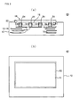
- Fig. 2(a) is a sectional view of the structure of a circuit module 60 including the IC 50 and the circuit substrate 10.
- Fig. 2(b) is a plan view of the circuit module 60.
- the plan view mentioned herein refers to a structure viewed in the direction of the normal to the circuit module 60.
- the circuit substrate 10 is a base on which an electronic component, or the IC 50, is to be surface-mounted, and includes a substrate 12, terminals 14 and internal conductive layers 16, as shown in Fig. 1 .
- the substrate 12 includes a stack of a plurality of insulating ceramic layers.
- the substrate 12 has a recess 15 formed by recessing part of the mounting surface thereof on which the IC 50 is to be mounted.
- the upper surface of the substrate 12 is referred to as the mounting surface
- the surface of the substrate 12 opposing the mounting surface is referred to as the lower surface.
- the mounting surface refers to the visible surface in plan view. More specifically, the mounting surface includes the face defined by the region outside the recess 15 and the face defined by the region within the recess 15. Recessing means that part of the circuit substrate 10 is deformed by compression.
- the internal conductive layers 16 are stacked with the ceramic layers to form the substrate 12.
- the internal conductive layers 16 are connected each other through via conductors (not shown) to form a circuit.
- the terminals 14 are formed in an array manner in the recess 15 so as to protrude from the mounting surface of the substrate 12, and serve to electrically connect the circuit including the internal conductive layers 16 with the IC 50. Hence, one ends of the terminals 14 are electrically connected to the internal conductive layers 16.
- the level of the terminal 14 is lower than the level of the mounting surface of the substrate 12 outside the recess 15.
- the IC 50 includes an IC body 52 and solder bumps 54.
- the IC body 52 includes a silicon substrate having a circuit (not shown).
- the solder bumps 54 are formed in an array manner on the lower surface of the IC body 52, and serve to electrically connect the circuit of the IC body 52 with the terminals 14.
- the upper surface of the IC body 52 is referred to as the upper surface
- the lower surface of the IC body 52 is referred to as the mounting surface.
- the circuit substrate 10 and the IC 50 are aligned such that the terminals 14 come in contact with the respective solder bumps 54, as shown in Fig. 1 , and are then reflowed.
- the solder bumps 54 are thus melted to cover the terminals 14, as shown in Fig. 2(a) . Consequently, the IC 50 is mounted on the circuit substrate 10.
- the area of the recess 15 in plan view is smaller than that of the IC body 52.
- the IC body 52 is mounted so as to cover the recess 15 beyond the edges of the recess 15 when the circuit module 60 is viewed from above, as shown in Fig. 2(b) .
- the mounting surface of the IC body 52 is in contact with the mounting surface of the substrate 12, as shown in Fig. 2(a) .
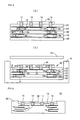
- FIGS. 3 to 6 are sectional views of the circuit substrate 10 in a manufacturing process.
- a binder, a plasticizer and a solvent are mixed to a ceramic material powder containing barium oxide, silicon oxide and alumina to prepare a slurry.
- the slurry is formed into a sheet on a carrier film to prepare a ceramic green sheet by a doctor blade method or any other sheet forming technique.
- the ceramic green sheet is cut into pieces having a predetermined size.
- a conductive paste mainly containing a conductive material, such as Cu or Ag is filled with via conductors 34, as shown in Fig. 3(b) .
- a conductive paste mainly containing a conductive material, such as Cu or Ag is printed on the main surface of the ceramic green sheet 20 to form an internal conductive layer 16 having a predetermined pattern.
- One of the layers constituting the substrate 12 is thus completed through the steps shown in Figs. 3(a) to 3(c) .
- the series of the steps shown in Figs. 3(a) to 3(c) is repeated until all the layers constituting the substrate are completed.
- the uppermost layer of the substrate 12 is formed using one of the ceramic green sheets. More specifically, a resin paste mainly containing polypropylene, butyral or acrylic resin is screen-printed on part of the main surface of the ceramic green sheet 20 to form a mask layer 30, as shown in Fig. 4(a) .
- the ceramic green sheet 20 and the mask layer 30 are subjected to stamping together to form through-holes 32 passing through the ceramic green sheet 20 and the mask layer 30, as shown in Fig. 4(b) .
- the through-holes 32 are filled with a conductive paste mainly containing a conductive material, such as Cu or Ag, to form terminals 14, as shown in Fig. 4(c) .
- the mask layer 30 and a plurality of ceramic green sheets 20 are stacked in such a manner that the mask layer 30 overlies the ceramic green sheets 20 so as to act as the uppermost layer.
- a carrier film 22 is removed from each ceramic green sheet 20 before stacking the layers.
- a multilayer green composite 40 is completed.
- the multilayer green composite 40 is placed in a base mold 42, and the multilayer green composite 40 is compressed by applying a pressure using a mold cover 44 from above to bind the ceramic green sheets 20 and the mask layer 30 together, as shown in Fig. 5(b) .
- the compression is performed under conditions of a mold cover 44 temperature of 70°C and a mold cover 44 pressure of 400 kg/cm 2 .
- the ceramic green sheets 20 under the mask layer 30 is compressed by the mask layer 30 in the thickness direction, so that the mask layer 30 is embedded in the uppermost ceramic green sheet 20, as shown in Fig. 6 .
- the recess 15 is formed.
- the internal conductive layers 16 are bent in such a manner that the portions of the internal conductive layers 16 under the mask layer 30 sink downwards, as shown in Fig. 6 .
- the boundaries between the ceramic green sheets 20, and the via conductors 34 are omitted.
- the multilayer green composite 40 including the ceramic green sheets 20 is fired.
- the mask layer 30 is consumed (burned down) due to high temperature, and the recess 15 appears.
- the firing is performed at 990°C for 1 hour.
- the circuit substrate 10 as shown in Fig. 1 is thus completed through the above-described process.
- the circuit substrate 10 has a recess 15 formed by recessing part of the mounting surface of the substrate 12, and terminals 14 are formed in the recess 15. Consequently, the distance from the lower surface of the circuit substrate 10 to the top of the terminal 14 (that is, the height of the circuit substrate) can be smaller than the height of a semiconductor device substrate having a flat mounting surface as disclosed in Patent Document 1. Thus, the thicknesses of the circuit substrate 10 and the circuit module 60 can be reduced. This will be described in detail below.
- the semiconductor device substrate disclosed in Patent Document 1 has columnar bumps protruding from the substrate, and a bump-forming sheet corresponding to the mask layer 30 is disposed as the uppermost layer over the entire surface of the substrate. Accordingly, a force is substantially evenly placed on the mounting surface of the substrate for compression, and a recess is not formed in the mounting surface of the substrate.
- the portions of the ceramic green sheets 20 under the mask layer 30 receive a higher pressure for compression than the other portions of the ceramic green sheets 20. Consequently, the compression in the stacking direction of the portions of the ceramic green sheets 20 under the mask layer 30 becomes larger by the thickness of the mask layer 30 than that of the other portions of the ceramic green sheets 20 and that of the substrate of Patent Document 1.
- the height of the circuit substrate 10 is more reduced by the thickness of the mask layer 30 than that of the semiconductor device substrate.
- the thicknesses of the circuit substrate 10 and the circuit module 60 including the circuit substrate 10 can be reduced.
- Fig. 7 is a sectional view of the structure of a circuit module 360 according to a reference embodiment. Let the distance between the mounting surface of the substrate 12 and the mounting surface of the IC body 52 be h1 in Fig. 2(a) . Also, in Fig. 7 , let the distance between the mounting surface of the substrate 312 and the mounting surface of the IC body 352 be h2.
- an IC 350 is mounted on a circuit substrate 310 whose mounting surface does not have a recess.
- the terminals 314 can be inserted in the solder bumps 354 to a larger depth than those of the circuit module 60 shown in Fig. 2 . Accordingly, the distance h2 between the mounting surface of the substrate 312 and the mounting surface of the IC body 352 is smaller than the distance h1 between the substrate 12 and the IC body 52.
- the volume of the terminal 14 embedded in the solder bump 54 in the circuit module 60 shown in Fig. 2 is smaller than that in the circuit module 360 shown in Fig. 7 . Accordingly, the form of the solder bump 54 of the circuit module 60 shown in Fig. 2 becomes smaller than that of the solder bump 354 of the circuit module 360 shown in Fig. 7 . Consequently, the distances between the solder bumps 54 in the circuit module 60 become larger than those in the circuit module 360, thus preventing short-circuiting.
- the through-holes 32 are formed in the ceramic green sheet 20 and the mask layer 30 at one time in the step shown in Fig. 4(b) . This can prevent the misalignment between the through-holes 32 formed in the ceramic green sheet 20 and the through-holes 32 formed in the mask layer 30. This will be further described below.
- the through-holes 32 of the mask layer 30 and the through-holes 32 of the ceramic green sheet 20 are formed in different steps.
- the through-holes 32 are formed in the ceramic green sheet 20 and the mask layer 30 separately, and then the mask layer 30 is disposed on the ceramic green sheet 20. Therefore, the through-holes 32 of the ceramic green sheet 20 and the through-holes 32 of the mask layer 30 can be misaligned unless the mask layer 30 is disposed on the ceramic green sheet 20 with precise alignment.
- the through-holes 32 are formed in the ceramic green sheet 20 and the mask layer 30 at one time, thus preventing misalignment of the through-holes 32.
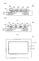
- Fig. 8(a) is a sectional view of the structure of a circuit module 160 including an IC 150 and a circuit substrate 110.
- Fig. 8(b) is a plan view of the circuit module 160. In the following description, differences of the circuit module 160 from the circuit module 60 of the first embodiment will be mainly described.
- the area of the recess 115 in plan view is larger than that of the IC body 152. Accordingly, the IC body 152 is disposed within the recess 115 when the circuit module 160 is viewed from above, as shown in Fig. 8(b) . In this state, the level of the mounting surface of the IC body 152 is lower than the level of the mounting surface of the substrate 112 outside the region of the recess 115, as shown in Fig. 8(a) .
- the distance from the lower surface of the substrate 112 to the upper surface of the IC body 152 (that is, the height of the circuit module 160) is shorter than the distance from the lower surface of the substrate 12 to the upper surface of the IC body 52 (that is, the height of the circuit module 60).
- the thickness of the circuit module 160 can be more reduced than that of the circuit module 60. It is preferable that the circuit module 160 be designed to have such a height as can maintain distances between the solder bumps 154 so as to prevent short-circuiting.
- Fig. 9 is a sectional view of the structure of a circuit module 260 including an IC 250 and a circuit substrate 210.
- differences of the circuit module 260 from the circuit module 60 of the first embodiment will be mainly described.
- the circuit substrate 210 includes a substrate 212 and a frame portion 217 rising from the mounting surface along the sides of the mounting surface.
- the frame portion 217 loops so as to surround the mounting surface of the substrate 212.
- the frame portion 217 is formed such that the level of the upper surface thereof is higher than that of the upper surface of the IC body 252. This structure allows the IC 250 to be sealed by filling the region surrounded by the frame portion 217 with a resin.
- the mounting surface of the substrate 212 refers to the region surrounded by the frame portion 217, not including the upper surface of the frame portion 217.
- the upper surface of the frame portion 217 lies at a level higher than the upper surface of the IC body 252.
- the structure of the circuit substrate 210 allows the distance from the lower surface of the substrate 212 to the upper surface of the IC body 252 to be reduced, as in the circuit substrate 10. Consequently, the level of the upper surface of the frame portion 217 can be lowered by the degree in which the level of the IC body 252 lowers.
- the distance from the lower surface of the substrate 212 to the upper surface of the frame portion 217 that is, the height of the circuit module 260
- the thicknesses of the circuit substrate 210 and the circuit module 260 can be reduced.
- the circuit substrate 210 can be manufacture by the following method. A method for manufacturing the circuit substrate 210 will now be described with reference to Figs. 10 and 11 .
- Fig. 10(a) is a sectional view of a ceramic green sheet 221.
- Fig. 10(b) is a plan view of the ceramic green sheet 221.
- Fig. 11 is a sectional view showing a step of the manufacturing process of the circuit substrate 210.
- the ceramic green sheet 221 defines the frame portion 217, and has such a shape as is formed by stamping the center of a rectangular sheet, as shown in Fig. 10(b) .
- a carrier film 222 is bonded to the rear surface of the ceramic green sheet 221.
- the ceramic green sheet 221 is disposed on the multilayer green composite 40 shown in Fig. 6 after the carrier has been removed therefrom, and then compression bonding is performed. The compression bonding is performed at a pressure of 200 kg/cm 2 .
- the resulting composite is referred to as a multilayer green composite 240.
- the multilayer green composite 240 includes two ceramic green sheets 221.
- the multilayer green composite 240 is fired in the same manner as in the method of the circuit substrate 10 according to the first embodiment.
- the mask layer 230 is burned down and removed due to high temperature and the recess 215 appears.
- the circuit substrate 210 as shown in Fig. 9 is thus completed through the above-described process.
- Figs. 12 and 13 are sectional views showing steps of a manufacturing process of the circuit substrate 210 according to a reference embodiment.
- a mask layer 430 is formed of a resin sheet, but not a resin paste. This process will be described in detail below.
- the mask layer is formed so as to cover the entire surface of the uppermost ceramic green sheet 220, as shown in Fig. 12 .
- additional ceramic green sheets 221 intended for the frame portion 217 are disposed on the mask layer 430.
- the ceramic green sheets 220, the ceramic green sheets 221 and the mask layer 430 are compressed together, thereby forming a multilayer green composite.
- the multilayer green composite is fired.
- the mask layer 430 is burned down and removed due to high temperature.
- the ceramic green sheets 221 disposed on the mask layer 430 as shown in Fig. 12 is separated from the substrate 212, as shown in Fig. 13 , by removing the mask layer 430.
- the circuit substrate manufacturing method using the resin sheet cannot produce the circuit substrate 210.
- the mask layer 230 is formed of a resin paste on part of the upper surface of the ceramic green sheet 220.
- the mask layer 230 is not present between the ceramic green sheet 220 and the ceramic green sheets 221. Consequently, the frame portion 217 is not separated from the substrate 212 by firming.
- Fig. 14 is a sectional view of the structure of a circuit module 460 including an IC 450 and a circuit substrate 410. In the following description, differences of the circuit module 460 from the circuit module 60 of the second embodiment will be mainly described.
- circuit module 60 has a circuit substrate 410 including an IC 450 and an electronic component 470 while the circuit module 60 has a circuit substrate 10 including only the IC 50. More specifically, the substrate 412 has land electrodes 418 used for mounting an electronic component 470 on the mounting surface outside the recess 415. The electronic component 470 is disposed on the land electrodes 418 with a solder layer 472 therebetween.
- FIG. 15 to 17 are sectional views of the circuit module 460 in steps of the manufacturing process.
- land electrodes 418 are formed on the mounting surface outside the recess 415, as shown in Fig. 15 .
- the land electrodes 418 are formed by, for example, applying an electroconductive paste mainly containing Cu, followed by firing. The firing of the land electrodes 418 may be performed simultaneously with the firing of the multilayer composite.
- a metal mask 480 having openings corresponding to the terminals 414 and the land electrodes 418 is aligned on the circuit substrate 410. Then, a squeegee 482 is moved on the metal mask 480 in the arrow direction to print a solder paste 484 through the metal mask 480. Thus, solder layers 472 and 474 are printed on the terminals 414 and the land electrode 418, as shown in Fig. 17 . Subsequently, an electronic component 470 and an IC 450 are mounted to complete the circuit module 460 shown in Fig. 14 .
- Fig. 18 is a sectional view of the structure of a circuit substrate 510 according to a reference embodiment.
- the circuit substrate 510 shown in Fig. 18 is different from the circuit substrate 410 shown in Fig. 14 in that the recess 415 is not formed.
- the metal mask 580 is disposed on the circuit substrate 510, and a solder paste 584 is printed using a squeegee 582.
- the metal mask 580 In order to prevent the solder layers from being displaced when the solder paste 584 is printed, the metal mask 580 should be disposed close to the mounting surface of the substrate 510. However, the circuit substrate 510 shown in Fig. 18 has terminals 514 protruding upward from the mounting surface of the substrate 512. If the metal mask 580 is disposed excessively close to the circuit substrate 510 to prevent the solder layers from being displaced or undesirably spreading, the squeegee 582 may come in contact with the terminals 514 to break the terminals 514.
- the metal mask 580 is disposed excessively distant from the mounting surface of the circuit substrate 510 to prevent the terminals 514 from being broken, the printed solder layers are displaced or undesirably spread because of the large distance between the metal mask 580 and the terminals 514 and land electrodes 518.
- the terminals 414 are formed within the recess 415. Consequently, the possibility that the squeegee 582 comes into contact with the land electrodes 418 is low even though the metal mask 480 is disposed close to the land electrodes 418.
- the distance between the land electrodes 418 and the metal mask 480 in the circuit substrate 410 can be more reduced than that in the circuit substrate 510, as shown in Figs. 16 and 18 . Accordingly, the displacement and undesired spread of the printed solder layer 472 can be prevented particularly on the land electrodes 418.
- circuit substrate 410 and the circuit module 460 according to the fourth embodiment may be produced by the following manufacturing method.
- Figs. 19 to 22 are sectional views of the circuit module 460 in steps of the manufacturing process.
- land electrodes 418 are formed on the mounting surface outside the recess 415, as shown in Fig. 15 .
- the land electrodes 418 are formed by, for example, applying an electroconductive paste mainly containing Cu, followed by firing. The firing of the land electrodes 418 may be performed simultaneously with the firing of the multilayer composite.
- a metal mask 480 having openings corresponding to the land electrodes 418 is aligned on the circuit substrate 410.
- This metal mask 480 does not have openings corresponding to the terminals 414.
- a squeegee 482 is moved on the metal mask 480 in the arrow direction to print a solder paste 484 through the metal mask 480.
- solder layers 472 are printed on the land electrodes 418, as shown in Fig. 20 .
- an electronic component 470 is mounted on the land electrodes 418 with the solder layers 472 therebetween, as shown in Fig. 21 .
- an IC 450 having solder bumps 454 coated with a flux 456 is disposed on the terminals 414, as shown in Fig. 22 .
- the reflowing temperature for mounting the electronic component 470 and the IC 450 is, for example, 260°C.
- the circuit module 460 is thus completed through the above-described process.
- Fig. 23 is a sectional view of the structure of a circuit substrate 610 according to a reference embodiment.
- the circuit substrate 610 shown in Fig. 23 is different from the circuit substrate 410 shown in Fig. 14 in that the recess 415 is not formed.
- the metal mask 680 is disposed on the circuit substrate 610, and a solder paste 684 is printed using a squeegee 682.
- the metal mask 680 In order to prevent the solder layers from being displaced when the solder paste 684 is printed, the metal mask 680 should be disposed close to the mounting surface of the substrate 610. However, the circuit substrate 610 shown in Fig. 23 has terminals 612 protruding upward from the mounting surface of the substrate 614. If the metal mask 680 is disposed excessively close to the circuit substrate 610 to prevent the solder layers from being displaced or undesirably spreading, the metal mask 680 may be pressed on the terminals 614 to crush the top ends of the terminals 614.
- the solder layers are displaced or undesirably spread because of the large distance between the metal mask 680 and the terminals 614 and land electrodes 618.
- the terminals 414 are formed within the recess 415. Consequently, the possibility that the metal mask 480 comes into contact with the land electrodes 418 is low even though the metal mask 480 is disposed close to the land electrodes 418.
- the distance between the land electrodes 418 and the metal mask 480 in the circuit substrate 410 can be more educed than that in the circuit substrate 610, as shown in Figs. 19 and 23 . Accordingly, the displacement and undesired spread of the printed solder layer 472 can be prevented particularly on the land electrodes 418.
- solder bumps 454 may be coated with a solder paste instead of the flux 456.
- the through-holes 24 and 32 in the circuit substrate 10 are formed by stamping, other techniques may be applied to form the through-holes 24 and 32.
- the through-holes 24 and 32 may be formed by laser beam machining. If the through-holes 32 are formed by laser beam machining, it is preferable that laser beam be irradiated from the mask layer 30 side. Since the energy of laser beam is consumed to reduce the diameter of the beam while forming the through-holes 32 in the ceramic green sheet 20, the diameter of the through-hole 32 is increased upward.
- the present invention is useful to circuit substrates, circuit modules and methods for manufacturing circuit substrates, and is particularly superior in that it can reduce the thicknesses of circuit substrates and circuit modules including circuit substrates.
Landscapes
- Engineering & Computer Science (AREA)
- Microelectronics & Electronic Packaging (AREA)
- Manufacturing & Machinery (AREA)
- Production Of Multi-Layered Print Wiring Board (AREA)
- Structures For Mounting Electric Components On Printed Circuit Boards (AREA)
- Wire Bonding (AREA)
Abstract
A circuit module (60) includes an IC (50) mounted on a circuit substrate (10). IC (50) includes an IC body (52) and an solder bump (54) formed on a mounting surface of the IC body (52). The circuit substrate (10) includes a substrate (12) having a recess (15) formed by recessing part of a mounting surface of the substrate on which the IC (50) is to be mounted, and a terminal (14) protruding from the mounting surface of the substrate (12). The terminal (14) is to be electrically connected to the solder bump (54).
Description
- The present invention relates to a circuit substrate, a circuit module and a method for manufacturing the circuit substrate, and more specifically to a circuit substrate on which electronic components are to be mounted, a circuit module and a method for manufacturing the circuit substrate.
- For mounting an electronic component, such as an IC, on a circuit substrate, the following technique is generally applied. Flat electrode pads are arranged in an array manner on the main surface of a circuit substrate. On the main surface of an IC, solder bumps are formed in an array manner. The IC is placed on the circuit substrate in such a manner that the solder bumps are aligned with the respective electrode pads, and the solder bumps are reflowed. The solder bumps are melted to fix the electrode pads, and the IC is thus mounted on the circuit substrate.
- However, the circuit substrate and the IC have different thermal expansion coefficients. Consequently, for example, the circuit substrate may be warped by heat, and, thus, this mounting technique may result in connection failure between the circuit substrate and the IC.
Accordingly,Patent Documents - The columnar bump has a larger height than the electrode pad and is accordingly elastic. Even if the circuit substrate is warped by heat, the columnar bump can absorb the warping. Thus, the semiconductor device substrates disclosed in
Patent Documents - Such a semiconductor device substrate however increases the height of the circuit substrate by the height of the columnar bumps.
- Patent Document 1: Japanese Patent No.
3203731 - Patent Document 2: Japanese Unexamined Patent Application Publication No.
2005-45143 - Accordingly, an object of the present invention is to provide a thin circuit substrate and circuit module that include protruding terminals, and a method for manufacturing the circuit substrate.
- A circuit substrate is provided on which a first electronic component having a bump is to be mounted. The circuit substrate includes a substrate having a mounting surface on which the first electronic component is to be disposed. The mounting surface has a recess formed by recessing part of the mounting surface. The circuit substrate also includes a terminal to be electrically connected to the bump of the first electronic component.
The terminal protrudes from the mounting surface within the recess. The circuit substrate may further include an electrode to which a second electronic component is to be joined. The electrode is disposed on the mounting surface outside the recess. - A circuit module is provided which includes a first electronic component, and a circuit substrate on which the first electronic component is mounted. The first electronic component includes an electronic component body and a bump formed on the electronic component body. The circuit substrate includes a substrate having a mounting surface on which the first electronic component is disposed and having a recess formed by recessing the mounting surface, and a terminal electrically connected to the bump and protruding from the mounting surface within the recess.
- According to the present invention, the recess is formed by recessing the mounting surface of the substrate. Consequently, the distance from the lower surface of the circuit substrate to the top of the terminal (that is, the height of the circuit substrate) can be smaller than the height of a semiconductor device substrate having a flat mounting surface. Thus, the thickness of a circuit substrate and a circuit module including the circuit substrate can be reduced.
- The electronic component body may be disposed within the recess when viewed in the direction of the normal to the substrate.
- Alternatively, the electronic component body may cover the recess beyond the edges of the recess when viewed in the direction of the normal to the substrate and be in contact with the substrate.
- The circuit module may further include a second electronic component. In this instance, the circuit substrate further includes an electrode on the mounting surface outside the recess. The second electronic component is joined to the electrode with a solder layer therebetween.
- The present invention further provides a method for manufacturing a circuit substrate. More specifically, the method manufactures a circuit substrate on which a first electronic component having a bump is to be mounted. The circuit substrate includes a terminal to which the bump of the first electronic component is to be electrically connected. The method includes the steps of: forming a mask layer on part of a main surface of a first sheet; forming a through-hole in the mask layer, filling the through-hole with a conductive material; stacking a plurality of second sheets and the first sheet having the mask layer such that the mask layer acts as the uppermost layer, and compressing the stack to embed the mask layer in the first sheet; and removing the mask layer from the stack of the first sheet and the second sheets.
- The mask layer may be formed by applying a resin paste onto the first sheet in the step of forming the mask layer.
- The through-hole may be formed by irradiating the mask layer with a laser beam in the step of forming the through-hole.
- In the method, the first sheet and the second sheets may be ceramic green sheets, and the mask layer may be made of a resin. In this instance, the step of removing the mask layer is performed by firing the first sheet and the second sheets together with the mask layer, thereby consuming the mask layer.
- The through-hole may be formed so as to pass through the first sheet and the mask layer in the step of forming the through-hole.
- The method may further include the steps of: forming an electrode in a region other than the mask layer, and printing a solder paste on the electrode through a mask pattern. The electrode is to be joined to a second electronic component.
- According to the present invention, the recess is formed by recessing part of the mounting surface of the substrate, and a terminal is formed within the recess. Consequently, the height of the circuit substrate can be lower than the height of a semiconductor device substrate having a flat mounting surface. Thus, the thickness of a circuit substrate and a circuit module including the circuit substrate can be reduced.
-
- [
Fig. 1] Fig. 1 is a sectional view of a structure in which an IC is aligned on a circuit substrate according to a first embodiment. - [
Fig. 2] Fig. 2(a) is a sectional view of the structure of a circuit module including an IC and a circuit substrate.Fig. 2(b) is a plan view of the circuit module. - [
Fig. 3] Fig. 3 is a representation including sectional views showing a manufacturing process of a circuit substrate. - [
Fig. 4] Fig. 4 is a representation including sectional views showing the manufacturing process of a circuit substrate. - [
Fig. 5] Fig. 5 is a representation including sectional views showing the manufacturing process of a circuit substrate. - [
Fig. 6] Fig. 6 is a representation of a sectional views showing the manufacturing process of a circuit substrate. - [
Fig. 7] Fig. 7 is a section view of the structure of a circuit module according to a reference embodiment. - [
Fig. 8] Fig. 8(a) is a sectional view of the structure of a circuit module including an IC and a circuit substrate according to a second embodiment.Fig. 8(b) is a plan view of the circuit module. - [
Fig. 9] Fig. 9 is a sectional view of the structure of a circuit module including an IC and a circuit substrate according to a third embodiment. - [
Fig. 10] Fig. 10(a) is a sectional view of the structure of a ceramic green sheet.Fig. 10(b) is a plan view of the ceramic green sheet. - [
Fig. 11] Fig. 11 is a sectional view showing a manufacturing process of a circuit substrate. - [
Fig. 12] Fig. 12 is a sectional view showing a manufacturing process of a circuit substrate according to a reference embodiment. - [
Fig. 13] Fig. 13 is a sectional view showing a manufacturing process of a circuit substrate according to a reference embodiment. - [
Fig. 14] Fig. 14 is a sectional view of the structure of a circuit module including an IC and a circuit substrate according to a fourth embodiment. - [
Fig. 15] Fig. 15 is a sectional view of a circuit module in a manufacturing process. - [
Fig. 16] Fig. 16 is a sectional view of a circuit module in a manufacturing process. - [
Fig. 17] Fig. 17 is a sectional view of a circuit module in a manufacturing process. - [
Fig. 18] Fig. 18 is a section view of the structure of a circuit substrate according to a reference embodiment. - [
Fig. 19] Fig. 19 is a sectional view of a circuit module in a manufacturing process. - [
Fig. 20] Fig. 20 is a sectional view of a circuit module in a manufacturing process. - [
Fig. 21] Fig. 21 is a sectional view of a circuit module in a manufacturing process. - [
Fig. 22] Fig. 22 is a sectional view of a circuit module in a manufacturing process. - [
Fig. 23] Fig. 23 is a section view of the structure of a circuit substrate according to a reference embodiment. - The circuit substrate, the circuit module and the method for manufacturing the circuit substrate according to the present invention will now be described.
- The structures of a circuit substrate and a circuit module according to a first embodiment will now be described with reference to related drawings.
Fig. 1 is a sectional view of the structure in which a semiconductor integrated circuit (hereinafter referred to as IC) 50 is aligned on acircuit substrate 10.Fig. 2(a) is a sectional view of the structure of acircuit module 60 including theIC 50 and thecircuit substrate 10.Fig. 2(b) is a plan view of thecircuit module 60. The plan view mentioned herein refers to a structure viewed in the direction of the normal to thecircuit module 60. - The
circuit substrate 10 is a base on which an electronic component, or theIC 50, is to be surface-mounted, and includes asubstrate 12,terminals 14 and internalconductive layers 16, as shown inFig. 1 . Thesubstrate 12 includes a stack of a plurality of insulating ceramic layers. Thesubstrate 12 has arecess 15 formed by recessing part of the mounting surface thereof on which theIC 50 is to be mounted. In the description hereinafter, the upper surface of thesubstrate 12 is referred to as the mounting surface, and the surface of thesubstrate 12 opposing the mounting surface is referred to as the lower surface. In the present embodiment, the mounting surface refers to the visible surface in plan view. More specifically, the mounting surface includes the face defined by the region outside therecess 15 and the face defined by the region within therecess 15. Recessing means that part of thecircuit substrate 10 is deformed by compression. - The internal
conductive layers 16 are stacked with the ceramic layers to form thesubstrate 12. The internalconductive layers 16 are connected each other through via conductors (not shown) to form a circuit. - The
terminals 14 are formed in an array manner in therecess 15 so as to protrude from the mounting surface of thesubstrate 12, and serve to electrically connect the circuit including the internalconductive layers 16 with theIC 50. Hence, one ends of theterminals 14 are electrically connected to the internalconductive layers 16. The level of the terminal 14 is lower than the level of the mounting surface of thesubstrate 12 outside therecess 15. - The
IC 50 includes anIC body 52 and solder bumps 54.
TheIC body 52 includes a silicon substrate having a circuit (not shown). The solder bumps 54 are formed in an array manner on the lower surface of theIC body 52, and serve to electrically connect the circuit of theIC body 52 with theterminals 14. In the description hereinafter, the upper surface of theIC body 52 is referred to as the upper surface, and the lower surface of theIC body 52 is referred to as the mounting surface. - The
circuit substrate 10 and theIC 50 are aligned such that theterminals 14 come in contact with the respective solder bumps 54, as shown inFig. 1 , and are then reflowed. The solder bumps 54 are thus melted to cover theterminals 14, as shown inFig. 2(a) . Consequently, theIC 50 is mounted on thecircuit substrate 10. - The area of the
recess 15 in plan view is smaller than that of theIC body 52. Hence, theIC body 52 is mounted so as to cover therecess 15 beyond the edges of therecess 15 when thecircuit module 60 is viewed from above, as shown inFig. 2(b) . In this instance, the mounting surface of theIC body 52 is in contact with the mounting surface of thesubstrate 12, as shown inFig. 2(a) . - A method for manufacturing the
circuit substrate 10 will now be described with reference to related drawings.
Figs. 3 to 6 are sectional views of thecircuit substrate 10 in a manufacturing process. - First, a binder, a plasticizer and a solvent are mixed to a ceramic material powder containing barium oxide, silicon oxide and alumina to prepare a slurry. Subsequently, the slurry is formed into a sheet on a carrier film to prepare a ceramic green sheet by a doctor blade method or any other sheet forming technique. The ceramic green sheet is cut into pieces having a predetermined size.
- After the completion of the ceramic green sheets, layers constituting the
substrate 12 are formed. As shown inFig. 3(a) , first, through-holes 24 are formed in one of the ceramicgreen sheets 20 by stamping. Then, the through-holes 24 are filled with a conductive paste mainly containing a conductive material, such as Cu or Ag, to form viaconductors 34, as shown inFig. 3(b) . - Subsequently, a conductive paste mainly containing a conductive material, such as Cu or Ag, is printed on the main surface of the ceramic
green sheet 20 to form an internalconductive layer 16 having a predetermined pattern. One of the layers constituting thesubstrate 12 is thus completed through the steps shown inFigs. 3(a) to 3(c) .
The series of the steps shown inFigs. 3(a) to 3(c) is repeated until all the layers constituting the substrate are completed. - Then, the uppermost layer of the
substrate 12 is formed using one of the ceramic green sheets. More specifically, a resin paste mainly containing polypropylene, butyral or acrylic resin is screen-printed on part of the main surface of the ceramicgreen sheet 20 to form amask layer 30, as shown inFig. 4(a) . - After the formation of the
mask layer 30, the ceramicgreen sheet 20 and themask layer 30 are subjected to stamping together to form through-holes 32 passing through the ceramicgreen sheet 20 and themask layer 30, as shown inFig. 4(b) . Then, the through-holes 32 are filled with a conductive paste mainly containing a conductive material, such as Cu or Ag, to formterminals 14, as shown inFig. 4(c) . - Turning now to
Fig. 5(a) , themask layer 30 and a plurality of ceramicgreen sheets 20 are stacked in such a manner that themask layer 30 overlies the ceramicgreen sheets 20 so as to act as the uppermost layer. In practice, acarrier film 22 is removed from each ceramicgreen sheet 20 before stacking the layers. Thus, a multilayergreen composite 40 is completed. - Subsequently, the multilayer
green composite 40 is placed in abase mold 42, and the multilayergreen composite 40 is compressed by applying a pressure using amold cover 44 from above to bind the ceramicgreen sheets 20 and themask layer 30 together, as shown inFig. 5(b) . The compression is performed under conditions of amold cover 44 temperature of 70°C and amold cover 44 pressure of 400 kg/cm2. Thus, the ceramicgreen sheets 20 under themask layer 30 is compressed by themask layer 30 in the thickness direction, so that themask layer 30 is embedded in the uppermost ceramicgreen sheet 20, as shown inFig. 6 . Thus, therecess 15 is formed. At this time, the internalconductive layers 16 are bent in such a manner that the portions of the internalconductive layers 16 under themask layer 30 sink downwards, as shown inFig. 6 . InFig. 6 , the boundaries between the ceramicgreen sheets 20, and the viaconductors 34 are omitted. - Finally, the multilayer
green composite 40 including the ceramicgreen sheets 20 is fired. At this time, themask layer 30 is consumed (burned down) due to high temperature, and therecess 15 appears. The firing is performed at 990°C for 1 hour. Thecircuit substrate 10 as shown inFig. 1 is thus completed through the above-described process. - The
circuit substrate 10 has arecess 15 formed by recessing part of the mounting surface of thesubstrate 12, andterminals 14 are formed in therecess 15. Consequently, the distance from the lower surface of thecircuit substrate 10 to the top of the terminal 14 (that is, the height of the circuit substrate) can be smaller than the height of a semiconductor device substrate having a flat mounting surface as disclosed inPatent Document 1. Thus, the thicknesses of thecircuit substrate 10 and thecircuit module 60 can be reduced. This will be described in detail below. - The semiconductor device substrate disclosed in
Patent Document 1 has columnar bumps protruding from the substrate, and a bump-forming sheet corresponding to themask layer 30 is disposed as the uppermost layer over the entire surface of the substrate. Accordingly, a force is substantially evenly placed on the mounting surface of the substrate for compression, and a recess is not formed in the mounting surface of the substrate. - On the other hand, for forming the
circuit substrate 10, the portions of the ceramicgreen sheets 20 under themask layer 30 receive a higher pressure for compression than the other portions of the ceramicgreen sheets 20. Consequently, the compression in the stacking direction of the portions of the ceramicgreen sheets 20 under themask layer 30 becomes larger by the thickness of themask layer 30 than that of the other portions of the ceramicgreen sheets 20 and that of the substrate ofPatent Document 1. Thus, the height of thecircuit substrate 10 is more reduced by the thickness of themask layer 30 than that of the semiconductor device substrate. Hence, the thicknesses of thecircuit substrate 10 and thecircuit module 60 including thecircuit substrate 10 can be reduced. - Since the
recess 15 is smaller than theIC body 52 when viewed from above, as shown inFig. 2(b) , the mounting surface of theIC body 52 comes in contact with the mounting surface of thesubstrate 12 when theIC 50 is mounted on thecircuit substrate 10. Consequently, thesubstrate 12 and theIC body 52 can maintain a distance to some extent therebetween so as to prevent the solder bumps 54 from being excessively compressed to cause a short circuit between adjacent solder bumps 54. The reason will be described below with reference toFigs. 2 and7. Fig. 7 is a sectional view of the structure of acircuit module 360 according to a reference embodiment. Let the distance between the mounting surface of thesubstrate 12 and the mounting surface of theIC body 52 be h1 inFig. 2(a) . Also, inFig. 7 , let the distance between the mounting surface of the substrate 312 and the mounting surface of theIC body 352 be h2. - In the
circuit module 360 shown inFig. 7 , anIC 350 is mounted on acircuit substrate 310 whose mounting surface does not have a recess. In this instance, since the mounting surface of theIC body 352 does not come in contact with the mounting surface of the substrate 312, theterminals 314 can be inserted in the solder bumps 354 to a larger depth than those of thecircuit module 60 shown inFig. 2 . Accordingly, the distance h2 between the mounting surface of the substrate 312 and the mounting surface of theIC body 352 is smaller than the distance h1 between thesubstrate 12 and theIC body 52. - If the
solder bump 54 and thesolder bump 354 have the same volume before mounting, the volume of the terminal 14 embedded in thesolder bump 54 in thecircuit module 60 shown inFig. 2 is smaller than that in thecircuit module 360 shown inFig. 7 . Accordingly, the form of thesolder bump 54 of thecircuit module 60 shown inFig. 2 becomes smaller than that of thesolder bump 354 of thecircuit module 360 shown inFig. 7 . Consequently, the distances between the solder bumps 54 in thecircuit module 60 become larger than those in thecircuit module 360, thus preventing short-circuiting. - For the
circuit module 60, the through-holes 32 are formed in the ceramicgreen sheet 20 and themask layer 30 at one time in the step shown inFig. 4(b) . This can prevent the misalignment between the through-holes 32 formed in the ceramicgreen sheet 20 and the through-holes 32 formed in themask layer 30. This will be further described below. - If the
mask layer 30 is formed of, for example, a resin sheet, but not of a resin paste, the through-holes 32 of themask layer 30 and the through-holes 32 of the ceramicgreen sheet 20 are formed in different steps. In this instance, the through-holes 32 are formed in the ceramicgreen sheet 20 and themask layer 30 separately, and then themask layer 30 is disposed on the ceramicgreen sheet 20. Therefore, the through-holes 32 of the ceramicgreen sheet 20 and the through-holes 32 of themask layer 30 can be misaligned unless themask layer 30 is disposed on the ceramicgreen sheet 20 with precise alignment. For thecircuit module 60, on the other hand, the through-holes 32 are formed in the ceramicgreen sheet 20 and themask layer 30 at one time, thus preventing misalignment of the through-holes 32. - The structures of a circuit substrate and a circuit module according to a second embodiment will now be described with reference to related drawings.
Fig. 8(a) is a sectional view of the structure of acircuit module 160 including anIC 150 and acircuit substrate 110.Fig. 8(b) is a plan view of thecircuit module 160. In the following description, differences of thecircuit module 160 from thecircuit module 60 of the first embodiment will be mainly described. - In the
circuit module 160, the area of therecess 115 in plan view is larger than that of theIC body 152. Accordingly, theIC body 152 is disposed within therecess 115 when thecircuit module 160 is viewed from above, as shown inFig. 8(b) . In this state, the level of the mounting surface of theIC body 152 is lower than the level of the mounting surface of thesubstrate 112 outside the region of therecess 115, as shown inFig. 8(a) . Thus, the distance from the lower surface of thesubstrate 112 to the upper surface of the IC body 152 (that is, the height of the circuit module 160) is shorter than the distance from the lower surface of thesubstrate 12 to the upper surface of the IC body 52 (that is, the height of the circuit module 60). Hence, the thickness of thecircuit module 160 can be more reduced than that of thecircuit module 60. It is preferable that thecircuit module 160 be designed to have such a height as can maintain distances between the solder bumps 154 so as to prevent short-circuiting. - The structures of a circuit substrate and a circuit module according to a third embodiment will now be described with reference to related drawings.
Fig. 9 is a sectional view of the structure of acircuit module 260 including anIC 250 and acircuit substrate 210. In the following description, differences of thecircuit module 260 from thecircuit module 60 of the first embodiment will be mainly described. - The
circuit substrate 210 includes asubstrate 212 and aframe portion 217 rising from the mounting surface along the sides of the mounting surface. Theframe portion 217 loops so as to surround the mounting surface of thesubstrate 212. Also, theframe portion 217 is formed such that the level of the upper surface thereof is higher than that of the upper surface of theIC body 252. This structure allows theIC 250 to be sealed by filling the region surrounded by theframe portion 217 with a resin. In the present embodiment, the mounting surface of thesubstrate 212 refers to the region surrounded by theframe portion 217, not including the upper surface of theframe portion 217. - The upper surface of the
frame portion 217 lies at a level higher than the upper surface of theIC body 252. The structure of thecircuit substrate 210 allows the distance from the lower surface of thesubstrate 212 to the upper surface of theIC body 252 to be reduced, as in thecircuit substrate 10. Consequently, the level of the upper surface of theframe portion 217 can be lowered by the degree in which the level of theIC body 252 lowers. In thecircuit module 260, the distance from the lower surface of thesubstrate 212 to the upper surface of the frame portion 217 (that is, the height of the circuit module 260) can thus be reduced. Hence, the thicknesses of thecircuit substrate 210 and thecircuit module 260 can be reduced. - The
circuit substrate 210 can be manufacture by the following method. A method for manufacturing thecircuit substrate 210 will now be described with reference toFigs. 10 and11 .Fig. 10(a) is a sectional view of a ceramicgreen sheet 221.Fig. 10(b) is a plan view of the ceramicgreen sheet 221.Fig. 11 is a sectional view showing a step of the manufacturing process of thecircuit substrate 210. - The ceramic
green sheet 221 defines theframe portion 217, and has such a shape as is formed by stamping the center of a rectangular sheet, as shown inFig. 10(b) . Acarrier film 222 is bonded to the rear surface of the ceramicgreen sheet 221. The ceramicgreen sheet 221 is disposed on the multilayergreen composite 40 shown inFig. 6 after the carrier has been removed therefrom, and then compression bonding is performed. The compression bonding is performed at a pressure of 200 kg/cm2. The resulting composite is referred to as a multilayergreen composite 240. The multilayergreen composite 240 includes two ceramicgreen sheets 221. - Subsequently, the multilayer
green composite 240 is fired in the same manner as in the method of thecircuit substrate 10 according to the first embodiment. In this step, themask layer 230 is burned down and removed due to high temperature and therecess 215 appears. Thecircuit substrate 210 as shown inFig. 9 is thus completed through the above-described process. - The above-describe method of the present embodiment can provide a
circuit substrate 210 having theframe portion 217. The detail will be described below with reference toFigs. 12 and 13. Figs. 12 and 13 are sectional views showing steps of a manufacturing process of thecircuit substrate 210 according to a reference embodiment. In the process according to the reference embodiment, amask layer 430 is formed of a resin sheet, but not a resin paste. This process will be described in detail below. - In the method according to the reference embodiment, the mask layer is formed so as to cover the entire surface of the uppermost ceramic
green sheet 220, as shown inFig. 12 . Then, additional ceramicgreen sheets 221 intended for theframe portion 217 are disposed on themask layer 430.
The ceramicgreen sheets 220, the ceramicgreen sheets 221 and themask layer 430 are compressed together, thereby forming a multilayer green composite. The multilayer green composite is fired. In this step, themask layer 430 is burned down and removed due to high temperature. The ceramicgreen sheets 221 disposed on themask layer 430 as shown inFig. 12 is separated from thesubstrate 212, as shown inFig. 13 , by removing themask layer 430. Hence, the circuit substrate manufacturing method using the resin sheet cannot produce thecircuit substrate 210. - In the circuit substrate manufacturing method according to the third embodiment, on the other hand, the
mask layer 230 is formed of a resin paste on part of the upper surface of the ceramicgreen sheet 220. Thus, themask layer 230 is not present between the ceramicgreen sheet 220 and the ceramicgreen sheets 221. Consequently, theframe portion 217 is not separated from thesubstrate 212 by firming. - The structures of a circuit substrate and a circuit module according to a fourth embodiment will now be described with reference to related drawings.
Fig. 14 is a sectional view of the structure of acircuit module 460 including anIC 450 and acircuit substrate 410. In the following description, differences of thecircuit module 460 from thecircuit module 60 of the second embodiment will be mainly described. - The difference between the
circuit module 60 and thecircuit module 460 is that thecircuit module 460 has acircuit substrate 410 including anIC 450 and anelectronic component 470 while thecircuit module 60 has acircuit substrate 10 including only theIC 50. More specifically, thesubstrate 412 hasland electrodes 418 used for mounting anelectronic component 470 on the mounting surface outside therecess 415. Theelectronic component 470 is disposed on theland electrodes 418 with asolder layer 472 therebetween. - A method for manufacturing the
circuit module 460 will now be described with reference to related drawings.Figs. 15 to 17 are sectional views of thecircuit module 460 in steps of the manufacturing process. - First, the steps shown in
Figs. 3 to 6 are performed in the same manner as in the manufacturing process of thecircuit substrate 10 according to the first embodiment, and the same description will be omitted. Subsequently,land electrodes 418 are formed on the mounting surface outside therecess 415, as shown inFig. 15 . Theland electrodes 418 are formed by, for example, applying an electroconductive paste mainly containing Cu, followed by firing. The firing of theland electrodes 418 may be performed simultaneously with the firing of the multilayer composite. - Turning now to
Fig. 16 , ametal mask 480 having openings corresponding to theterminals 414 and theland electrodes 418 is aligned on thecircuit substrate 410.
Then, asqueegee 482 is moved on themetal mask 480 in the arrow direction to print asolder paste 484 through themetal mask 480. Thus, solder layers 472 and 474 are printed on theterminals 414 and theland electrode 418, as shown inFig. 17 . Subsequently, anelectronic component 470 and anIC 450 are mounted to complete thecircuit module 460 shown inFig. 14 . - The
circuit substrate 410 of the present embodiment can prevent theterminals 414 from breaking, and prevent the solder layers 472 from being displaced and undesirably spreading, as described below with reference to related drawings.Fig. 18 is a sectional view of the structure of acircuit substrate 510 according to a reference embodiment. - The
circuit substrate 510 shown inFig. 18 is different from thecircuit substrate 410 shown inFig. 14 in that therecess 415 is not formed. In order to print solder layers on theterminals 514 and theland electrodes 518 of such acircuit substrate 510, themetal mask 580 is disposed on thecircuit substrate 510, and asolder paste 584 is printed using asqueegee 582. - In order to prevent the solder layers from being displaced when the
solder paste 584 is printed, themetal mask 580 should be disposed close to the mounting surface of thesubstrate 510. However, thecircuit substrate 510 shown inFig. 18 hasterminals 514 protruding upward from the mounting surface of thesubstrate 512. If themetal mask 580 is disposed excessively close to thecircuit substrate 510 to prevent the solder layers from being displaced or undesirably spreading, thesqueegee 582 may come in contact with theterminals 514 to break theterminals 514. On the other hand, if themetal mask 580 is disposed excessively distant from the mounting surface of thecircuit substrate 510 to prevent theterminals 514 from being broken, the printed solder layers are displaced or undesirably spread because of the large distance between themetal mask 580 and theterminals 514 andland electrodes 518. - On the other hand, in the
circuit substrate 410 having therecess 415, theterminals 414 are formed within therecess 415. Consequently, the possibility that thesqueegee 582 comes into contact with theland electrodes 418 is low even though themetal mask 480 is disposed close to theland electrodes 418. In addition, the distance between theland electrodes 418 and themetal mask 480 in thecircuit substrate 410 can be more reduced than that in thecircuit substrate 510, as shown inFigs. 16 and 18 . Accordingly, the displacement and undesired spread of the printedsolder layer 472 can be prevented particularly on theland electrodes 418. - The
circuit substrate 410 and thecircuit module 460 according to the fourth embodiment may be produced by the following manufacturing method.Figs. 19 to 22 are sectional views of thecircuit module 460 in steps of the manufacturing process. - First, the steps shown in
Figs. 3 to 6 are performed in the same manner as in the manufacturing process of thecircuit substrate 10 of the first embodiment, and the same description will be omitted. Subsequently,land electrodes 418 are formed on the mounting surface outside therecess 415, as shown inFig. 15 . Theland electrodes 418 are formed by, for example, applying an electroconductive paste mainly containing Cu, followed by firing. The firing of theland electrodes 418 may be performed simultaneously with the firing of the multilayer composite. - Turning now to
Fig. 19 , ametal mask 480 having openings corresponding to theland electrodes 418 is aligned on thecircuit substrate 410. Thismetal mask 480 does not have openings corresponding to theterminals 414. Then, asqueegee 482 is moved on themetal mask 480 in the arrow direction to print asolder paste 484 through themetal mask 480. Thus, solder layers 472 are printed on theland electrodes 418, as shown inFig. 20 . - Subsequently, an
electronic component 470 is mounted on theland electrodes 418 with thesolder layers 472 therebetween, as shown inFig. 21 . Then, anIC 450 havingsolder bumps 454 coated with aflux 456 is disposed on theterminals 414, as shown inFig. 22 . The reflowing temperature for mounting theelectronic component 470 and theIC 450 is, for example, 260°C. Thecircuit module 460 is thus completed through the above-described process. - The
circuit substrate 410 of the present embodiment can prevent the top ends of theterminals 414 from being crushed, and prevent the solder layers 472 from being displaced and undesirably spreading, as described below with reference to related drawing.Fig. 23 is a sectional view of the structure of acircuit substrate 610 according to a reference embodiment. - The
circuit substrate 610 shown inFig. 23 is different from thecircuit substrate 410 shown inFig. 14 in that therecess 415 is not formed. In order to print solder layers on theterminals 614 and theland electrodes 618 of such acircuit substrate 610, themetal mask 680 is disposed on thecircuit substrate 610, and asolder paste 684 is printed using asqueegee 682. - In order to prevent the solder layers from being displaced when the
solder paste 684 is printed, themetal mask 680 should be disposed close to the mounting surface of thesubstrate 610. However, thecircuit substrate 610 shown inFig. 23 hasterminals 612 protruding upward from the mounting surface of thesubstrate 614. If themetal mask 680 is disposed excessively close to thecircuit substrate 610 to prevent the solder layers from being displaced or undesirably spreading, themetal mask 680 may be pressed on theterminals 614 to crush the top ends of theterminals 614. On the other hand, if themetal mask 680 is disposed excessively distant from the mounting surface of thecircuit substrate 610 to prevent theterminals 614 from being crushed, the solder layers are displaced or undesirably spread because of the large distance between themetal mask 680 and theterminals 614 andland electrodes 618. - On the other hand, in the
circuit substrate 410 having therecess 415, theterminals 414 are formed within therecess 415. Consequently, the possibility that themetal mask 480 comes into contact with theland electrodes 418 is low even though themetal mask 480 is disposed close to theland electrodes 418. In addition, the distance between theland electrodes 418 and themetal mask 480 in thecircuit substrate 410 can be more educed than that in thecircuit substrate 610, as shown inFigs. 19 and23 . Accordingly, the displacement and undesired spread of the printedsolder layer 472 can be prevented particularly on theland electrodes 418. - The solder bumps 454 may be coated with a solder paste instead of the
flux 456. - Although the through-
holes circuit substrate 10 are formed by stamping, other techniques may be applied to form the through-holes holes holes 32 are formed by laser beam machining, it is preferable that laser beam be irradiated from themask layer 30 side. Since the energy of laser beam is consumed to reduce the diameter of the beam while forming the through-holes 32 in the ceramicgreen sheet 20, the diameter of the through-hole 32 is increased upward. - As described above, the present invention is useful to circuit substrates, circuit modules and methods for manufacturing circuit substrates, and is particularly superior in that it can reduce the thicknesses of circuit substrates and circuit modules including circuit substrates.
Claims (12)
- A circuit substrate on which a first electronic component having a bump is to be mounted, the circuit substrate comprising: a substrate having a mounting surface on which the first electronic component is to be disposed, the mounting surface having a recess formed by recessing part of the mounting surface; and a terminal to be electrically connected to the bump of the first electronic component, the terminal protruding from the mounting surface within the recess.
- The circuit substrate according to Claim 1, further comprising an electrode on the mounting surface outside the recess, the electrode being to be joined to a second electronic component.
- A circuit module comprising a first electronic component; and a circuit substrate on which the first electronic component is mounted, wherein the first electronic component includes an electronic component body and a bump formed on the electronic component body, and the circuit substrate includes a substrate having a mounting surface on which the first electronic component is disposed and having a recess formed by recessing part of the mounting surface, and a terminal protruding from the mounting surface within the recess and electrically connected to the bump.
- The circuit module according to Claim 3, wherein the electronic component body is disposed within the recess when viewed in the direction of the normal to the substrate.
- The circuit module according to Claim 3, wherein the electronic component body covers the recess beyond the edges of the recess when viewed in the direction of the normal to the substrate and is in contact with the substrate.
- The circuit module according to Claim 3 or 4, further comprising a second electronic component, wherein the circuit substrate further includes an electrode on the mounting surface outside the recess, and the second electronic component is joined to the electrode with a solder layer therebetween.
- A method for manufacturing a circuit substrate on which a first electronic component having a bump is to be mounted, the circuit substrate including a terminal to which the bump of the first electronic component is to be electrically connected, the method comprising the steps of: forming a mask layer on part of a main surface of a first sheet; forming a through-hole in the mask layer; filling the through-hole with a conductive material; stacking a plurality of second sheets and the first sheet having the mask layer such that the mask layer acts as the uppermost layer, and compressing the stack to embed the mask layer in the first sheet; and removing the mask layer from the stack of the first sheet and the second sheets.
- The method according to Claim 7, wherein the mask layer is formed by applying a resin paste onto the first sheet in the step of forming the mask layer.
- The method according to Claim 7 or 8, wherein the through-hole is formed by irradiating the mask layer with a laser beam in the step of forming the through-hole.
- The method according to any one of Claims 7 to 9, wherein the first sheet and the second sheets are ceramic green sheets, and the mask layer is made of a resin, and wherein the step of removing the mask layer is performed by firing the first sheet and the second sheets together with the mask layer, thereby consuming the mask layer.
- The method according to any one of Claims 7 to 10, wherein the through-hole is formed so as to pass through the first sheet and the mask layer in the step of forming the through-hole.
- The method according to any one of Claims 7 to 11, further comprising the steps of: forming an electrode to which a second electronic component is to be joined, in a region other than the mask layer; and printing a solder paste on the electrode through a mask pattern.
Applications Claiming Priority (3)
| Application Number | Priority Date | Filing Date | Title |
|---|---|---|---|
| JP2007231314 | 2007-09-06 | ||
| JP2008092195 | 2008-03-31 | ||
| PCT/JP2008/065897 WO2009031588A1 (en) | 2007-09-06 | 2008-09-03 | Circuit board, circuit module and circuit board manufacturing method |
Publications (3)
| Publication Number | Publication Date |
|---|---|
| EP2187717A1 true EP2187717A1 (en) | 2010-05-19 |
| EP2187717A4 EP2187717A4 (en) | 2011-04-13 |
| EP2187717B1 EP2187717B1 (en) | 2012-06-20 |
Family
ID=40428902
Family Applications (1)
| Application Number | Title | Priority Date | Filing Date |
|---|---|---|---|
| EP08829892A Not-in-force EP2187717B1 (en) | 2007-09-06 | 2008-09-03 | Circuit board manufacturing method |
Country Status (4)
| Country | Link |
|---|---|
| US (2) | US20100147573A1 (en) |
| EP (1) | EP2187717B1 (en) |
| JP (2) | JP4337950B2 (en) |
| WO (1) | WO2009031588A1 (en) |
Cited By (2)
| Publication number | Priority date | Publication date | Assignee | Title |
|---|---|---|---|---|
| CN107424973A (en) * | 2016-05-23 | 2017-12-01 | 恒劲科技股份有限公司 | Package substrate and method for fabricating the same |
| EP3799539A1 (en) * | 2019-09-27 | 2021-03-31 | Siemens Aktiengesellschaft | Circuit carrier, package and method for its production |
Families Citing this family (10)
| Publication number | Priority date | Publication date | Assignee | Title |
|---|---|---|---|---|
| JP5113114B2 (en) * | 2009-04-06 | 2013-01-09 | 新光電気工業株式会社 | Wiring board manufacturing method and wiring board |
| JP5553234B2 (en) * | 2010-09-29 | 2014-07-16 | 澁谷工業株式会社 | Conductive ball mounting device |
| TWI446590B (en) * | 2010-09-30 | 2014-07-21 | 億光電子工業股份有限公司 | Light-emitting diode package structure and manufacturing method thereof |
| US20140074571A1 (en) * | 2012-09-10 | 2014-03-13 | Super Transcon Ip, Llc | Commerce System and Method of Controlling the Commerce System by Layering Contextual Advertisements Over a Graphical Interface |
| JP2014072372A (en) * | 2012-09-28 | 2014-04-21 | Ibiden Co Ltd | Printed wiring board manufacturing method and printed wiring board |
| CN104253884A (en) * | 2013-06-28 | 2014-12-31 | 深圳富泰宏精密工业有限公司 | Shell and method for manufacturing same |
| US9349614B2 (en) * | 2014-08-06 | 2016-05-24 | Invensas Corporation | Device and method for localized underfill |
| JP6955864B2 (en) * | 2016-12-26 | 2021-10-27 | ラピスセミコンダクタ株式会社 | Semiconductor devices and methods for manufacturing semiconductor devices |
| EP3848988B1 (en) * | 2020-01-09 | 2025-12-31 | Murata Manufacturing Co., Ltd. | METHOD FOR PRODUCING A SEMICONDUCTOR STRUCTURE WITH IMPROVED DIVISION PROPERTIES |
| WO2021192739A1 (en) * | 2020-03-27 | 2021-09-30 | 株式会社村田製作所 | Module and method for manufacturing same |
Family Cites Families (19)
| Publication number | Priority date | Publication date | Assignee | Title |
|---|---|---|---|---|
| US4896464A (en) * | 1988-06-15 | 1990-01-30 | International Business Machines Corporation | Formation of metallic interconnects by grit blasting |
| JP3203731B2 (en) | 1992-02-05 | 2001-08-27 | 松下電器産業株式会社 | Semiconductor element substrate and mounting method, substrate with columnar terminals and method of manufacturing the same |
| KR0179404B1 (en) * | 1993-02-02 | 1999-05-15 | 모리시타 요이찌 | Ceramic substrate and manufacturing method thereof |
| US5629835A (en) * | 1994-07-19 | 1997-05-13 | Olin Corporation | Metal ball grid array package with improved thermal conductivity |
| JP2000077467A (en) * | 1998-08-31 | 2000-03-14 | Matsushita Electric Works Ltd | Semiconductor device |
| JP2001223295A (en) * | 2000-02-08 | 2001-08-17 | Hitachi Chem Co Ltd | Semiconductor element support substrate, method of manufacturing the same, and semiconductor device using the same |
| US6507119B2 (en) * | 2000-11-30 | 2003-01-14 | Siliconware Precision Industries Co., Ltd. | Direct-downset flip-chip package assembly and method of fabricating the same |
| KR100891269B1 (en) * | 2001-01-31 | 2009-04-06 | 소니 가부시끼 가이샤 | Semiconductor device and manufacturing method thereof |
| JP2004056115A (en) * | 2002-05-31 | 2004-02-19 | Ngk Spark Plug Co Ltd | Multilayer wiring board |
| JP2004311795A (en) * | 2003-04-09 | 2004-11-04 | Sumitomo Metal Electronics Devices Inc | Package for storing semiconductor elements |
| JP4016340B2 (en) * | 2003-06-13 | 2007-12-05 | ソニー株式会社 | Semiconductor device, mounting structure thereof, and manufacturing method thereof |
| JP2005045143A (en) | 2003-07-25 | 2005-02-17 | Murata Mfg Co Ltd | Method for manufacturing ceramic substrate with projection electrode |
| TWI228809B (en) * | 2003-08-07 | 2005-03-01 | Advanced Semiconductor Eng | Flip chip package structure and substrate structure thereof |
| JP4128945B2 (en) * | 2003-12-04 | 2008-07-30 | 松下電器産業株式会社 | Semiconductor device |
| JP2005311225A (en) * | 2004-04-26 | 2005-11-04 | Tdk Corp | Method for manufacturing laminated electronic component |
| JP4581643B2 (en) * | 2004-11-19 | 2010-11-17 | 株式会社村田製作所 | Manufacturing method of multilayer ceramic substrate |
| JP4852991B2 (en) * | 2005-11-18 | 2012-01-11 | 株式会社村田製作所 | Electronic components |
| US8188375B2 (en) * | 2005-11-29 | 2012-05-29 | Tok Corporation | Multilayer circuit board and method for manufacturing the same |
| US20080186690A1 (en) * | 2007-02-07 | 2008-08-07 | Nokia Corporation | Electronics Package And Manufacturing Method Thereof |
-
2008
- 2008-09-03 WO PCT/JP2008/065897 patent/WO2009031588A1/en not_active Ceased
- 2008-09-03 JP JP2008558128A patent/JP4337950B2/en not_active Expired - Fee Related
- 2008-09-03 EP EP08829892A patent/EP2187717B1/en not_active Not-in-force
-
2009
- 2009-05-01 JP JP2009111745A patent/JP5278149B2/en not_active Expired - Fee Related
-
2010
- 2010-03-04 US US12/717,171 patent/US20100147573A1/en not_active Abandoned
-
2012
- 2012-09-14 US US13/616,102 patent/US9185805B2/en not_active Expired - Fee Related
Cited By (5)
| Publication number | Priority date | Publication date | Assignee | Title |
|---|---|---|---|---|
| CN107424973A (en) * | 2016-05-23 | 2017-12-01 | 恒劲科技股份有限公司 | Package substrate and method for fabricating the same |
| CN107424973B (en) * | 2016-05-23 | 2020-01-21 | 凤凰先驱股份有限公司 | Package substrate and its manufacturing method |
| EP3799539A1 (en) * | 2019-09-27 | 2021-03-31 | Siemens Aktiengesellschaft | Circuit carrier, package and method for its production |
| US11153977B2 (en) | 2019-09-27 | 2021-10-19 | Siemens Aktiengesellschaft | Circuit carrier, package, and method for manufacturing a package |
| US11723155B2 (en) | 2019-09-27 | 2023-08-08 | Siemens Aktiengesellschaft | Circuit carrier, package, and method for manufacturing a package |
Also Published As
| Publication number | Publication date |
|---|---|
| JP4337950B2 (en) | 2009-09-30 |
| EP2187717B1 (en) | 2012-06-20 |
| US20100147573A1 (en) | 2010-06-17 |
| JP5278149B2 (en) | 2013-09-04 |
| WO2009031588A1 (en) | 2009-03-12 |
| JPWO2009031588A1 (en) | 2010-12-16 |
| US9185805B2 (en) | 2015-11-10 |
| US20130008586A1 (en) | 2013-01-10 |
| JP2009267421A (en) | 2009-11-12 |
| EP2187717A4 (en) | 2011-04-13 |
Similar Documents
| Publication | Publication Date | Title |
|---|---|---|
| EP2187717B1 (en) | Circuit board manufacturing method | |
| TWI407870B (en) | Wiring substrate manufacturing method | |
| EP2141972B1 (en) | Component-incorporating module and its manufacturing method | |
| US6509531B2 (en) | Monolithic ceramic electronic component, method for manufacturing the same, and electronic device | |
| EP3349244B1 (en) | Electronic component housing package, multi-piece wiring substrate, electronic device, and electronic module | |
| JP4337949B2 (en) | Circuit board and circuit board manufacturing method | |
| JP5803345B2 (en) | Semiconductor chip manufacturing method, circuit package and manufacturing method thereof | |
| KR20090051627A (en) | Multilayer Ceramic Substrate and Manufacturing Method Thereof | |
| US7302757B2 (en) | Micro-bumps to enhance LGA interconnections | |
| JP2005268672A (en) | substrate | |
| JPH11163054A (en) | Semiconductor device structure and method of manufacturing the same | |
| US20050151303A1 (en) | Method for producing ceramic substrate and electronic component module using ceramic substrate | |
| CN103181246A (en) | Composite substrate, module, and method of producing composite substrate | |
| JP2000340715A (en) | Wiring board for mounting semiconductor element and semiconductor device using the same | |
| JP2004128134A (en) | Ceramic laminated substrate and method of manufacturing the same | |
| JP4038610B2 (en) | Manufacturing method of ceramic substrate | |
| JP2004356527A (en) | Circuit board, electronic device using the same, and method of manufacturing the same | |
| JP2005136235A (en) | Wiring board | |
| JP2004247393A (en) | Method for manufacturing semiconductor device | |
| JP2010219181A (en) | Electronic component module, and method of mounting electronic component | |
| JP2012146950A (en) | Wiring substrate, wiring substrate with solder bump, electronic device, and method of manufacturing wiring substrate with solder bump | |
| JP2003142633A (en) | Wiring board manufacturing method | |
| KR20110117779A (en) | Method for manufacturing circuit board | |
| JP2003163241A (en) | Component connection structure for electronic circuits | |
| JP2006173158A (en) | Electronic component mounting method |
Legal Events
| Date | Code | Title | Description |
|---|---|---|---|
| PUAI | Public reference made under article 153(3) epc to a published international application that has entered the european phase |
Free format text: ORIGINAL CODE: 0009012 |
|
| 17P | Request for examination filed |
Effective date: 20100202 |
|
| AK | Designated contracting states |
Kind code of ref document: A1 Designated state(s): AT BE BG CH CY CZ DE DK EE ES FI FR GB GR HR HU IE IS IT LI LT LU LV MC MT NL NO PL PT RO SE SI SK TR |
|
| AX | Request for extension of the european patent |
Extension state: AL BA MK RS |
|
| DAX | Request for extension of the european patent (deleted) | ||
| A4 | Supplementary search report drawn up and despatched |
Effective date: 20110310 |
|
| GRAP | Despatch of communication of intention to grant a patent |
Free format text: ORIGINAL CODE: EPIDOSNIGR1 |
|
| RIC1 | Information provided on ipc code assigned before grant |
Ipc: H05K 1/11 20060101ALI20111201BHEP Ipc: H01L 23/16 20060101ALI20111201BHEP Ipc: H01L 23/498 20060101ALI20111201BHEP Ipc: H01L 21/60 20060101ALI20111201BHEP Ipc: H05K 3/46 20060101ALI20111201BHEP Ipc: H05K 1/18 20060101AFI20111201BHEP Ipc: H01L 23/13 20060101ALI20111201BHEP Ipc: H05K 3/40 20060101ALI20111201BHEP Ipc: H01L 21/48 20060101ALI20111201BHEP |
|
| RTI1 | Title (correction) |
Free format text: CIRCUIT BOARD MANUFACTURING METHOD |
|
| GRAS | Grant fee paid |
Free format text: ORIGINAL CODE: EPIDOSNIGR3 |
|
| GRAA | (expected) grant |
Free format text: ORIGINAL CODE: 0009210 |
|
| AK | Designated contracting states |
Kind code of ref document: B1 Designated state(s): AT BE BG CH CY CZ DE DK EE ES FI FR GB GR HR HU IE IS IT LI LT LU LV MC MT NL NO PL PT RO SE SI SK TR |
|
| REG | Reference to a national code |
Ref country code: GB Ref legal event code: FG4D |
|
| REG | Reference to a national code |
Ref country code: CH Ref legal event code: EP |
|
| REG | Reference to a national code |
Ref country code: AT Ref legal event code: REF Ref document number: 563625 Country of ref document: AT Kind code of ref document: T Effective date: 20120715 |
|
| REG | Reference to a national code |
Ref country code: IE Ref legal event code: FG4D |
|
| REG | Reference to a national code |
Ref country code: DE Ref legal event code: R096 Ref document number: 602008016563 Country of ref document: DE Effective date: 20120823 |
|
| PG25 | Lapsed in a contracting state [announced via postgrant information from national office to epo] |
Ref country code: LT Free format text: LAPSE BECAUSE OF FAILURE TO SUBMIT A TRANSLATION OF THE DESCRIPTION OR TO PAY THE FEE WITHIN THE PRESCRIBED TIME-LIMIT Effective date: 20120620 Ref country code: FI Free format text: LAPSE BECAUSE OF FAILURE TO SUBMIT A TRANSLATION OF THE DESCRIPTION OR TO PAY THE FEE WITHIN THE PRESCRIBED TIME-LIMIT Effective date: 20120620 Ref country code: NO Free format text: LAPSE BECAUSE OF FAILURE TO SUBMIT A TRANSLATION OF THE DESCRIPTION OR TO PAY THE FEE WITHIN THE PRESCRIBED TIME-LIMIT Effective date: 20120920 Ref country code: SE Free format text: LAPSE BECAUSE OF FAILURE TO SUBMIT A TRANSLATION OF THE DESCRIPTION OR TO PAY THE FEE WITHIN THE PRESCRIBED TIME-LIMIT Effective date: 20120620 |
|
| REG | Reference to a national code |
Ref country code: NL Ref legal event code: VDEP Effective date: 20120620 |
|
| REG | Reference to a national code |
Ref country code: AT Ref legal event code: MK05 Ref document number: 563625 Country of ref document: AT Kind code of ref document: T Effective date: 20120620 |
|
| REG | Reference to a national code |
Ref country code: LT Ref legal event code: MG4D Effective date: 20120620 |
|
| PG25 | Lapsed in a contracting state [announced via postgrant information from national office to epo] |
Ref country code: GR Free format text: LAPSE BECAUSE OF FAILURE TO SUBMIT A TRANSLATION OF THE DESCRIPTION OR TO PAY THE FEE WITHIN THE PRESCRIBED TIME-LIMIT Effective date: 20120921 Ref country code: HR Free format text: LAPSE BECAUSE OF FAILURE TO SUBMIT A TRANSLATION OF THE DESCRIPTION OR TO PAY THE FEE WITHIN THE PRESCRIBED TIME-LIMIT Effective date: 20120620 Ref country code: SI Free format text: LAPSE BECAUSE OF FAILURE TO SUBMIT A TRANSLATION OF THE DESCRIPTION OR TO PAY THE FEE WITHIN THE PRESCRIBED TIME-LIMIT Effective date: 20120620 Ref country code: LV Free format text: LAPSE BECAUSE OF FAILURE TO SUBMIT A TRANSLATION OF THE DESCRIPTION OR TO PAY THE FEE WITHIN THE PRESCRIBED TIME-LIMIT Effective date: 20120620 |
|
| PG25 | Lapsed in a contracting state [announced via postgrant information from national office to epo] |
Ref country code: CZ Free format text: LAPSE BECAUSE OF FAILURE TO SUBMIT A TRANSLATION OF THE DESCRIPTION OR TO PAY THE FEE WITHIN THE PRESCRIBED TIME-LIMIT Effective date: 20120620 Ref country code: AT Free format text: LAPSE BECAUSE OF FAILURE TO SUBMIT A TRANSLATION OF THE DESCRIPTION OR TO PAY THE FEE WITHIN THE PRESCRIBED TIME-LIMIT Effective date: 20120620 Ref country code: RO Free format text: LAPSE BECAUSE OF FAILURE TO SUBMIT A TRANSLATION OF THE DESCRIPTION OR TO PAY THE FEE WITHIN THE PRESCRIBED TIME-LIMIT Effective date: 20120620 Ref country code: IS Free format text: LAPSE BECAUSE OF FAILURE TO SUBMIT A TRANSLATION OF THE DESCRIPTION OR TO PAY THE FEE WITHIN THE PRESCRIBED TIME-LIMIT Effective date: 20121020 Ref country code: CY Free format text: LAPSE BECAUSE OF FAILURE TO SUBMIT A TRANSLATION OF THE DESCRIPTION OR TO PAY THE FEE WITHIN THE PRESCRIBED TIME-LIMIT Effective date: 20120620 Ref country code: EE Free format text: LAPSE BECAUSE OF FAILURE TO SUBMIT A TRANSLATION OF THE DESCRIPTION OR TO PAY THE FEE WITHIN THE PRESCRIBED TIME-LIMIT Effective date: 20120620 Ref country code: SK Free format text: LAPSE BECAUSE OF FAILURE TO SUBMIT A TRANSLATION OF THE DESCRIPTION OR TO PAY THE FEE WITHIN THE PRESCRIBED TIME-LIMIT Effective date: 20120620 Ref country code: BE Free format text: LAPSE BECAUSE OF FAILURE TO SUBMIT A TRANSLATION OF THE DESCRIPTION OR TO PAY THE FEE WITHIN THE PRESCRIBED TIME-LIMIT Effective date: 20120620 |
|
| PG25 | Lapsed in a contracting state [announced via postgrant information from national office to epo] |
Ref country code: IT Free format text: LAPSE BECAUSE OF FAILURE TO SUBMIT A TRANSLATION OF THE DESCRIPTION OR TO PAY THE FEE WITHIN THE PRESCRIBED TIME-LIMIT Effective date: 20120620 Ref country code: PT Free format text: LAPSE BECAUSE OF FAILURE TO SUBMIT A TRANSLATION OF THE DESCRIPTION OR TO PAY THE FEE WITHIN THE PRESCRIBED TIME-LIMIT Effective date: 20121022 Ref country code: PL Free format text: LAPSE BECAUSE OF FAILURE TO SUBMIT A TRANSLATION OF THE DESCRIPTION OR TO PAY THE FEE WITHIN THE PRESCRIBED TIME-LIMIT Effective date: 20120620 |
|
| PG25 | Lapsed in a contracting state [announced via postgrant information from national office to epo] |
Ref country code: NL Free format text: LAPSE BECAUSE OF FAILURE TO SUBMIT A TRANSLATION OF THE DESCRIPTION OR TO PAY THE FEE WITHIN THE PRESCRIBED TIME-LIMIT Effective date: 20120620 |
|
| PLBE | No opposition filed within time limit |
Free format text: ORIGINAL CODE: 0009261 |
|
| STAA | Information on the status of an ep patent application or granted ep patent |
Free format text: STATUS: NO OPPOSITION FILED WITHIN TIME LIMIT |
|
| PG25 | Lapsed in a contracting state [announced via postgrant information from national office to epo] |
Ref country code: MC Free format text: LAPSE BECAUSE OF NON-PAYMENT OF DUE FEES Effective date: 20120930 Ref country code: ES Free format text: LAPSE BECAUSE OF FAILURE TO SUBMIT A TRANSLATION OF THE DESCRIPTION OR TO PAY THE FEE WITHIN THE PRESCRIBED TIME-LIMIT Effective date: 20121001 Ref country code: DK Free format text: LAPSE BECAUSE OF FAILURE TO SUBMIT A TRANSLATION OF THE DESCRIPTION OR TO PAY THE FEE WITHIN THE PRESCRIBED TIME-LIMIT Effective date: 20120620 |
|
| REG | Reference to a national code |
Ref country code: CH Ref legal event code: PL |
|
| 26N | No opposition filed |
Effective date: 20130321 |
|
| GBPC | Gb: european patent ceased through non-payment of renewal fee |
Effective date: 20120920 |
|
| REG | Reference to a national code |
Ref country code: IE Ref legal event code: MM4A |
|
| REG | Reference to a national code |
Ref country code: FR Ref legal event code: ST Effective date: 20130531 |
|
| REG | Reference to a national code |
Ref country code: DE Ref legal event code: R097 Ref document number: 602008016563 Country of ref document: DE Effective date: 20130321 |
|
| PG25 | Lapsed in a contracting state [announced via postgrant information from national office to epo] |
Ref country code: IE Free format text: LAPSE BECAUSE OF NON-PAYMENT OF DUE FEES Effective date: 20120903 Ref country code: GB Free format text: LAPSE BECAUSE OF NON-PAYMENT OF DUE FEES Effective date: 20120920 Ref country code: BG Free format text: LAPSE BECAUSE OF FAILURE TO SUBMIT A TRANSLATION OF THE DESCRIPTION OR TO PAY THE FEE WITHIN THE PRESCRIBED TIME-LIMIT Effective date: 20120920 Ref country code: LI Free format text: LAPSE BECAUSE OF NON-PAYMENT OF DUE FEES Effective date: 20120930 Ref country code: CH Free format text: LAPSE BECAUSE OF NON-PAYMENT OF DUE FEES Effective date: 20120930 |
|
| PG25 | Lapsed in a contracting state [announced via postgrant information from national office to epo] |
Ref country code: FR Free format text: LAPSE BECAUSE OF NON-PAYMENT OF DUE FEES Effective date: 20121001 |
|
| PG25 | Lapsed in a contracting state [announced via postgrant information from national office to epo] |
Ref country code: MT Free format text: LAPSE BECAUSE OF FAILURE TO SUBMIT A TRANSLATION OF THE DESCRIPTION OR TO PAY THE FEE WITHIN THE PRESCRIBED TIME-LIMIT Effective date: 20120620 |
|
| PG25 | Lapsed in a contracting state [announced via postgrant information from national office to epo] |
Ref country code: TR Free format text: LAPSE BECAUSE OF FAILURE TO SUBMIT A TRANSLATION OF THE DESCRIPTION OR TO PAY THE FEE WITHIN THE PRESCRIBED TIME-LIMIT Effective date: 20120620 |
|
| PG25 | Lapsed in a contracting state [announced via postgrant information from national office to epo] |
Ref country code: LU Free format text: LAPSE BECAUSE OF NON-PAYMENT OF DUE FEES Effective date: 20120903 |
|
| PG25 | Lapsed in a contracting state [announced via postgrant information from national office to epo] |
Ref country code: HU Free format text: LAPSE BECAUSE OF FAILURE TO SUBMIT A TRANSLATION OF THE DESCRIPTION OR TO PAY THE FEE WITHIN THE PRESCRIBED TIME-LIMIT Effective date: 20080903 |
|
| PGFP | Annual fee paid to national office [announced via postgrant information from national office to epo] |
Ref country code: DE Payment date: 20200925 Year of fee payment: 13 |
|
| REG | Reference to a national code |
Ref country code: DE Ref legal event code: R119 Ref document number: 602008016563 Country of ref document: DE |
|
| PG25 | Lapsed in a contracting state [announced via postgrant information from national office to epo] |
Ref country code: DE Free format text: LAPSE BECAUSE OF NON-PAYMENT OF DUE FEES Effective date: 20220401 |