EP2184810B1 - Connecteur de carte - Google Patents
Connecteur de carte Download PDFInfo
- Publication number
- EP2184810B1 EP2184810B1 EP08827586.2A EP08827586A EP2184810B1 EP 2184810 B1 EP2184810 B1 EP 2184810B1 EP 08827586 A EP08827586 A EP 08827586A EP 2184810 B1 EP2184810 B1 EP 2184810B1
- Authority
- EP
- European Patent Office
- Prior art keywords
- terminals
- portions
- circuit board
- vertical
- vertical portions
- Prior art date
- Legal status (The legal status is an assumption and is not a legal conclusion. Google has not performed a legal analysis and makes no representation as to the accuracy of the status listed.)
- Not-in-force
Links
Images


Classifications
-
- H—ELECTRICITY
- H01—ELECTRIC ELEMENTS
- H01R—ELECTRICALLY-CONDUCTIVE CONNECTIONS; STRUCTURAL ASSOCIATIONS OF A PLURALITY OF MUTUALLY-INSULATED ELECTRICAL CONNECTING ELEMENTS; COUPLING DEVICES; CURRENT COLLECTORS
- H01R13/00—Details of coupling devices of the kinds covered by groups H01R12/70 or H01R24/00 - H01R33/00
- H01R13/648—Protective earth or shield arrangements on coupling devices, e.g. anti-static shielding
- H01R13/658—High frequency shielding arrangements, e.g. against EMI [Electro-Magnetic Interference] or EMP [Electro-Magnetic Pulse]
-
- H—ELECTRICITY
- H01—ELECTRIC ELEMENTS
- H01R—ELECTRICALLY-CONDUCTIVE CONNECTIONS; STRUCTURAL ASSOCIATIONS OF A PLURALITY OF MUTUALLY-INSULATED ELECTRICAL CONNECTING ELEMENTS; COUPLING DEVICES; CURRENT COLLECTORS
- H01R13/00—Details of coupling devices of the kinds covered by groups H01R12/70 or H01R24/00 - H01R33/00
- H01R13/646—Details of coupling devices of the kinds covered by groups H01R12/70 or H01R24/00 - H01R33/00 specially adapted for high-frequency, e.g. structures providing an impedance match or phase match
- H01R13/6461—Means for preventing cross-talk
-
- H—ELECTRICITY
- H01—ELECTRIC ELEMENTS
- H01R—ELECTRICALLY-CONDUCTIVE CONNECTIONS; STRUCTURAL ASSOCIATIONS OF A PLURALITY OF MUTUALLY-INSULATED ELECTRICAL CONNECTING ELEMENTS; COUPLING DEVICES; CURRENT COLLECTORS
- H01R13/00—Details of coupling devices of the kinds covered by groups H01R12/70 or H01R24/00 - H01R33/00
- H01R13/646—Details of coupling devices of the kinds covered by groups H01R12/70 or H01R24/00 - H01R33/00 specially adapted for high-frequency, e.g. structures providing an impedance match or phase match
- H01R13/6473—Impedance matching
- H01R13/6474—Impedance matching by variation of conductive properties, e.g. by dimension variations
-
- H—ELECTRICITY
- H01—ELECTRIC ELEMENTS
- H01R—ELECTRICALLY-CONDUCTIVE CONNECTIONS; STRUCTURAL ASSOCIATIONS OF A PLURALITY OF MUTUALLY-INSULATED ELECTRICAL CONNECTING ELEMENTS; COUPLING DEVICES; CURRENT COLLECTORS
- H01R13/00—Details of coupling devices of the kinds covered by groups H01R12/70 or H01R24/00 - H01R33/00
- H01R13/648—Protective earth or shield arrangements on coupling devices, e.g. anti-static shielding
- H01R13/658—High frequency shielding arrangements, e.g. against EMI [Electro-Magnetic Interference] or EMP [Electro-Magnetic Pulse]
- H01R13/6591—Specific features or arrangements of connection of shield to conductive members
- H01R13/6594—Specific features or arrangements of connection of shield to conductive members the shield being mounted on a PCB and connected to conductive members
-
- H—ELECTRICITY
- H01—ELECTRIC ELEMENTS
- H01R—ELECTRICALLY-CONDUCTIVE CONNECTIONS; STRUCTURAL ASSOCIATIONS OF A PLURALITY OF MUTUALLY-INSULATED ELECTRICAL CONNECTING ELEMENTS; COUPLING DEVICES; CURRENT COLLECTORS
- H01R12/00—Structural associations of a plurality of mutually-insulated electrical connecting elements, specially adapted for printed circuits, e.g. printed circuit boards [PCB], flat or ribbon cables, or like generally planar structures, e.g. terminal strips, terminal blocks; Coupling devices specially adapted for printed circuits, flat or ribbon cables, or like generally planar structures; Terminals specially adapted for contact with, or insertion into, printed circuits, flat or ribbon cables, or like generally planar structures
- H01R12/70—Coupling devices
- H01R12/71—Coupling devices for rigid printing circuits or like structures
- H01R12/72—Coupling devices for rigid printing circuits or like structures coupling with the edge of the rigid printed circuits or like structures
- H01R12/722—Coupling devices for rigid printing circuits or like structures coupling with the edge of the rigid printed circuits or like structures coupling devices mounted on the edge of the printed circuits
- H01R12/727—Coupling devices presenting arrays of contacts
-
- H—ELECTRICITY
- H01—ELECTRIC ELEMENTS
- H01R—ELECTRICALLY-CONDUCTIVE CONNECTIONS; STRUCTURAL ASSOCIATIONS OF A PLURALITY OF MUTUALLY-INSULATED ELECTRICAL CONNECTING ELEMENTS; COUPLING DEVICES; CURRENT COLLECTORS
- H01R13/00—Details of coupling devices of the kinds covered by groups H01R12/70 or H01R24/00 - H01R33/00
- H01R13/40—Securing contact members in or to a base or case; Insulating of contact members
- H01R13/405—Securing in non-demountable manner, e.g. moulding, riveting
- H01R13/41—Securing in non-demountable manner, e.g. moulding, riveting by frictional grip in grommet, panel or base
Definitions
- the present invention relates to a circuit board connector, and specifically relates to a circuit board connector to be attached to a printed circuit board on which printed wiring is provided in order to send and receive signals to and from the printed circuit board and supply electric power to the printed circuit board.
- an electrical/electronic appliance to be installed on a car such as an automobile is provided with a number of printed circuit boards on which electronic components, ICs (integrated circuits), and other components are mounted.
- ICs integrated circuits
- To the printed circuit boards electric wires arranged to send and receive signals to and from other devices and other printed circuit boards and supply electric power to the printed circuit boards are connected.
- circuit board connectors are used.
- a circuit board connector is generally configured such that a terminal arranged to send and receive signals is housed in a housing.
- a conventional circuit board connector 70 is configured such that a terminal 72 arranged to send and receive signals is housed in a dielectric 74, the dielectric 74 is sheathed with a shielding shell 76, and the shielding shell 76 is housed in a housing 78.
- the terminal 72 has a horizontal portion 72a to be connected to an end of an electric wire and a vertical portion 72b that extends downward from one end of the horizontal portion 72a in a vertical direction, which makes the terminal 72 have a substantially L shape.
- the plurality of terminals are often arranged in a plurality of layers in a height direction because of space limitations and other reasons.
- the path length of the upper terminal is made different from the path length of the lower terminal.
- JP 6-079085 A discloses a circuit board connector 80 in which terminals 82 are arranged in a plurality of layers in a height direction, as shown in Fig. 10 .
- an uppermost terminal 82a in a housing 84 is connected to a conductive region on a circuit board 86 that is closest to the housing 84
- a lowermost terminal 82b in the housing 84 is connected to a conductive region on the circuit board 86 that is farthest from the housing 84.
- lengths of the terminals 82 are substantially equal.
- the circuit board connector 80 of JP 6-079085 A is large in the depth direction because the lowermost terminal 82b in the housing 84 is made longer in the depth direction of the housing 84 in order to make the length of the lowermost terminal 82b in the housing 84 substantially equal to the length of the uppermost terminal 82a in the housing 84.
- the lowermost terminal 82b is connected to the conductive region on the circuit board 86 which is farther from the housing 84 than the conductive region on the circuit board 86 to which the uppermost terminal 82a is connected. Accordingly, the lowermost terminal 82b and the uppermost terminal 82a intersect with each other, and thus a delay (skew) of signals easily occurs.
- This known connector is suitable as a circuit board connector and comprises a plurality of terminals having horizontal portions arranged to be connected to ends of electric wires, and vertical portions extending downward from one end of the horizontal portions and arranged to be connected to a signal pattern of a printed circuit board.
- the horizontal portions of the plurality of terminals are arranged in a plurality of layers in a height direction, the vertical portions of the terminals having the horizontal portions in the upper layer are located on a back side in a depth direction with respect to the vertical portions of the terminals having the horizontal portions in the lower layer, and the vertical portions of the terminals in the lower layer are bent in the width direction.
- An object of the present invention still is to overcome the problems described above mainly with respect to JP 6-079085 A and to provide a circuit board connector which allows for preventing occurrence of a delay (skew) of signals without making the circuit board connector large in the depth direction and allows for preventing a crosstalk of signals.
- the vertical portions of the terminals in the lower layer are bent in the width direction so as to make a path length of the terminals in the upper layer and a path length of the terminals in the lower layer equal; and the plurality of terminals are housed in a housing comprising a plurality of insert holes into which the horizontal portions of the plurality of terminals are inserted and a plurality of receiving grooves arranged to receive the vertical portions of the plurality of terminals, and tip portions of the bent vertical portions of the terminals are received by the receiving grooves receiving base portions of the vertical portions of the adjacent terminals to said terminals.
- the plurality of terminals are preferably arranged substantially parallel to each other when viewed from the width direction.
- tip portions of the bent vertical portions of the terminals are received by the receiving grooves receiving the base portions of the vertical portions of the first adjacent terminals to said terminals.
- the upper terminals and the lower terminals do not intersect. Accordingly, a crosstalk of signals can be prevented.
- the path length of the upper terminals and the path length of the lower terminals are made equal by bending, occurrence of a delay (skew) of signals is prevented without making the circuit board connector large in the depth direction.
- the circuit board connector is made smaller in the depth direction.
- the receiving grooves are shared, which makes the connector smaller also in the width direction.
- a circuit board connector In a circuit board connector according to a preferred embodiment of the present invention, the side of the circuit board connector to be connected to an end of an electric wire is referred to as the front side, and the opposite side is referred to as the back side (the back side in the depth direction).
- An upper direction of a printed circuit board onto which the circuit board connector is attached is referred to as a height direction, and a direction that is perpendicular to both of the height direction and the depth direction is referred to as a width direction of the circuit board connector.
- a circuit board connector 10 is configured such that a plurality of terminals 12 arranged to electrically connect ends of electric wires and printed wiring of a printed circuit board are housed in an inner housing 14, the inner housing 14 is sheathed with a shielding shell 16 arranged to electromagnetically shield the plurality of terminals 12 and a shell cover 18 arranged to cover the shielding shell 16, and the shielding shell 16 is housed in an outer housing 20.
- the plurality of terminals 12 are preferably prepared by punching and bending a conductive plate material such as a metal plate material.
- the plurality of terminals 12 each include a horizontal portion 22 having a tab shape and arranged to be connected to a connecting terminal that is attached to the end of the electric wire, and a vertical portion 24 having a tab shape, extending downward from one end of the horizontal portion 22, and arranged to be connected to a signal pattern of the printed circuit board. Electrical connection of the vertical portion 24 to the signal pattern of the printed circuit board is performed by inserting the tip portion of the vertical portion 24 into a conductive through hole that is electrically connected to the signal pattern and then soldering the tip portion to the signal pattern.
- the plurality of terminals 12 are to be arranged in two layers in the height direction and in three rows in the width direction.
- each of upper terminals 12a in the upper layer in the height direction has a horizontal portion 22a that extends substantially linearly and a vertical portion 24a that extends downward substantially linearly from the horizontal portion 22a at a substantially right angle with respect to the horizontal portion 22a, and accordingly, the upper terminal 12a have a substantially L shape as a whole.
- Figs. 2A and 2B each of upper terminals 12a in the upper layer in the height direction has a horizontal portion 22a that extends substantially linearly and a vertical portion 24a that extends downward substantially linearly from the horizontal portion 22a at a substantially right angle with respect to the horizontal portion 22a, and accordingly, the upper terminal 12a have a substantially L shape as a whole.
- a lower terminal 12b in the lower layer in the height direction has a horizontal portion 22b that extends substantially linearly and a vertical portion 24b that first extends downward substantially linearly from the horizontal portion 22a at a substantially right angle with respect to the horizontal portions 22a, is then bent to extend obliquely downward in the width direction, and is additionally bent to extend downward in the vertical direction.
- the lower terminal 12b is configured such that the horizontal portion 22b forms a substantially right angle with the vertical portion 24b and that the vertical portion 24b has a substantially S shape.
- the inner housing 14 arranged to house the plurality of terminals 12 is made from an insulating resin material having a given dielectric constant and is located between the plurality of terminals 12 and the shielding shell 16 in order to insulate them.
- the inner housing 14 has a substantially box shape and includes a plurality of insert holes 26 into which the horizontal portions 22 of the plurality of terminals 12 are to be inserted.
- a plurality of receiving grooves 28 extending in the vertical direction perpendicular to the opening direction of the insert holes 26 and arranged to receive the vertical portions 24 of the plurality of terminals 12 are provided.
- Division walls 30 arranged to divide the receiving grooves 28 are provided at midpoint positions with cut portions 30a that extend obliquely downward. Each of the cut portions 30a connects one receiving groove 28 and the adjacent receiving groove 28, which allows for receiving the oblique portion of the vertical portion 24b of the lower terminal 12b.
- the receiving groove 28 has such a depth that both of the upper terminal 12a and the lower terminal 12b are received by the receiving groove 28 while being stacked.
- the plurality of terminals 12 are housed in the inner housing 14. As shown in Fig. 5A , the lower terminals 12b of the plurality of terminals 12 are first housed in the inner housing 14. The horizontal portions 22b of the lower terminals 12b are inserted into the insert holes 26 that are disposed in the lower layer in the inner housing 14, and the vertical portions 24b of the lower terminals 12b are received by the receiving grooves 28. Because the vertical portions 24 of the lower terminals 12b are bent in the width direction, housing the oblique portions of the vertical portions 24 in the cut portions 30a of the division walls 30 dividing the receiving grooves 28 positions the tip portions of the vertical portions 24 at the adjacent receiving grooves 28, and accordingly, the tip portions of the vertical portions 24 are received by the adjacent receiving grooves 28. In other words, the tip portions of the vertical portions 24b of the lower terminals 12 are received by the adjacent receiving grooves 28 to the receiving grooves 28 receiving the base portions of the vertical portions 24b.
- the upper terminals 12a are housed in the inner housing 14.
- the horizontal portions 22a of the upper terminals 12a are inserted into the insert holes 26 that are disposed in the upper layer in the inner housing 14, and the vertical portions 24a of the upper terminals 12a are received by the receiving grooves 28. Because the vertical portions 24a of the upper terminals 12a extend substantially linear, one vertical portion 24a of one upper terminal 12a is received by one receiving groove 28.
- the vertical portions 24a of the upper terminals 12a are received by the receiving grooves 28 receiving the vertical portions 24b of the lower terminals 12b in the state of being stacked but not being in contact with the lower terminals 12b, and are located on the back side in the depth direction with respect to the vertical portions 24b of the lower terminals 12b.
- the plurality of terminals 12 are arranged such that the horizontal portions 22 are arranged in a plurality of layers in the height direction and the vertical portions 24a of the upper terminals 12a are located on the back side in the depth direction with respect to the vertical portions 24b of the lower terminals 12b.
- the lower terminals 12b are located inside the upper terminals 12a, and the upper terminals 12a and the lower terminals 12b do not intersect with each other.
- the influence of signals transmitted through the upper terminals 12a (the lower terminals 12b) on signals transmitted through the lower terminals 12b (the upper terminals 12a) is made small, and a crosstalk of signals can be prevented in contrast to a connector in which upper terminals and lower terminals intersect with each other.
- the path length of the lower terminals 12b and the path length of the upper terminals 12a are made equal by bending the vertical portions 24b of the lower terminals 12b in the width direction and making the vertical portions 24b be long.
- a phase difference does not occur when signals are transmitted through the upper terminals 12a and the lower terminals 12b, and accordingly, a delay (a skew) of signals is prevented.
- an increase in the size of the connector in the depth direction is prevented, which brings about a great structural advantage.
- the tip portions of the vertical portions 24b of the lower terminals 12b are received by the adjacent receiving grooves 28 to the receiving grooves 28 receiving the base portions of the vertical portions 24b, and share the adjacent receiving grooves 28 with the base portions of the vertical portions 24b of the adjacent lower terminals 12b, which also makes the circuit board connector smaller in the width direction. In addition, it is not necessary to prepare separate receiving grooves 28 for receiving the tip portions of the vertical portions 24b, which makes the structure of the inner housing 14 more simplified.
- the path length of the lower terminals 12b is made longer by bending the vertical portions 24b in the width direction.
- the path length is preferably made longer by positioning the tip portion of the vertical portion 24b at a farther position, by enlarging the bend angle (the angle ⁇ in Fig. 3B ) of the vertical portion 24b, or by increasing the number of bendings of the vertical portion 24b.
- the path length of the lower terminals 12b is made equal to the path length of the upper terminals 12a.
- Examples of positioning the tip portion at a farther position include receiving the tip portion of the vertical portion 24b of the lower terminal 12b by the second or third adjacent receiving groove 28 to the receiving groove 28 receiving the base portion of the vertical portion 24b.
- the present invention is not limited to receiving the tip portion by the first adjacent receiving groove 28.
- the number of bendings may be three as shown in Fig. 6 , for example.
- the vertical portion 24b of the lower terminal 12b first extends downward substantially linearly at a substantially right angle with respect to the horizontal portion 22b, is then bent to extend obliquely downward in the width direction, is then bent to extend obliquely downward oppositely in the width direction, and is then bent to extend downward in the vertical direction.
- the tip portion of the vertical portion 24b of the lower terminal 12b is received by the receiving groove 28 receiving the base portion of the vertical portion 24b.
- the number of bendings of the lower terminal 12b in Fig. 6 is higher than the number of bendings of the lower terminal 12b in Fig. 5 , and the path length of the lower terminal 12b in Fig. 6 is longer than the path length of the lower terminal 12b in Fig. 5 .
- the arrangement of the plurality of terminals 12 is not limited to two layers in the height direction, and the plurality of terminals 12 may be arranged in three or more layers in the height direction. In addition, the arrangement of the plurality of terminals 12 is not limited to three rows in the width direction, and the plurality of terminals 12 may be arranged in one, two, or four or more rows.
- the upper terminals are located on the back side of the middle terminals in the depth direction
- the middle terminals are located on the back side of the lower terminals in the depth direction
- the order of path lengths from the longest to the shortest is the upper terminals, the middle terminals, and the lower terminals.
- the path length of the middle terminals and the path length of the lower terminals can be made equal to the path length of the upper terminals without intersecting with each other, and the connector is prevented from becoming larger in the depth direction.
- the lower terminals are required to be made much longer by using a different bending manner from the bending manner of the middle terminals because the path length of the lower terminals is shorter than the path length of the middle terminals.
- the vertical portion may be bent in the width direction such that the tip portion of the middle terminal is received by the first adjacent receiving groove, and the tip portion of the lower terminal is received by the second adjacent receiving groove.
- the bending angle of the lower terminal may be made greater than the bending angle of the middle terminal.
- the path length of the lower terminal may be made much longer by increasing the number of bendings of the lower terminal.
- the inner housing 14 housing the plurality of terminals 12 is housed in the shielding shell 16.
- the inner housing 14 has on the side walls engaging concave portions 32 arranged to be engaged and held in the shielding shell 16.
- the shielding shell 16 covering the inner housing 14 electromagnetically shields the plurality of terminals 12 housed in the inner housing 14.
- the shielding shell 16 is prepared by punching and bending a conductive plate material such as a metal plate material into a hollow body, and the inner housing 14 is housed in the hollow portion of the shielding shell 16.
- the shielding shell 16 has a substantially L shape in the same orientation as the upper terminals 12a when viewed from the width direction, and is provided with an engaging portion 34 having a rectangular tube shape extending in the horizontal direction and arranged to cover the horizontal portions 22 of the plurality of terminals 12, and a circuit board connecting portion 36 extending in the horizontal direction from the back side of the engaging portion 34 and arranged to connect the shielding shell 16 to the printed circuit board.
- the engaging portion 34 has on the side walls tongue-shaped spring portions 38 that are bent slightly inward, and the spring portions 38 are brought into elastic contact with engaging portions of an outer conductor terminal (a shielding shell) of a counterpart connector.
- the circuit board connecting portion 36 has on the side walls two pairs of tab-shaped leg portions 40 that are to be inserted into conductive through holes of the printed circuit board and extend downward in the vertical direction. By inserting and soldering the leg portions 40 into the through holes, the circuit board connecting portion 36 is electrically connected to the printed circuit board.
- a control projection portion 42 is disposed between each of the pairs of leg portions 40. The control projection portions 42 extend outward in the width direction from the side wall of the circuit board connecting portion 36 and are arranged to control the housing position of the shielding shell 16 by the outer housing 20.
- the shielding shell 16 opens on the back side, which allows the shielding shell 16 to house the inner housing 14 from the back side.
- the shielding shell 16 has engaging projection portions 44 on the side walls that project inward at positions corresponding to the engaging concave portions 32 of the inner housing 14.
- the engaging projection portions 44 of the shielding shell 16 are embedded in the engaging concave portions 32 of the inner housing 14 so as to engage and hold the inner housing 14 in the shielding shell 16.
- the shielding shell 36 On the back side of side walls 46 and a top wall 48, the shielding shell 36 has a plurality of engaging projection portions 50 that are arranged to engage and hold the shell cover 18 and project outward.
- the opening on the back side of the shielding shell 16 housing the inner housing 14 is covered with the shell cover 18.
- the shell cover 18 is prepared by punching a conductive plate material such as a metal plate material.
- the shell cover 18 has side walls 54 and a top wall 56 that extend from a main body wall 52 and are formed at right angles with the main body wall 52.
- the shell cover 18 has engaging holes 58 arranged to engage with the engaging projection portions 50 provided to the back side of the side walls 46 and the top wall 48 of the shielding shell 16.
- the engaging projection portions 50 of the shielding shell 16 engage with the engaging holes 58 of the shell cover 18, so that the shell cover 18 engages and holds the back side of the shielding shell 16.
- the shell cover 18 On the side walls 54 and the top wall 56, the shell cover 18 has control projection portions 60 that project outward and are arranged to control the housing position when the shielding shell 16 attached with the shell cover 18 is housed in the outer housing 20 from the back side.
- the outer housing 20 arranged to house the shielding shell 16 is prepared from an insulating resin material and has a substantially box shape.
- the outer housing 20 has on the front side a hood portion 62 arranged to house a counterpart connector to be mated with the hood portion 62 and in the top wall an engaging hole 64 arranged to engage with an engaging projection portion of a connector housing of a counterpart connector.
- the outer housing 20 has on the back side a housing portion 66 arranged to house the shielding shell 16 and extending from the hood portion 62.
- the housing portion 66 opens on the back side and on the lower side, which allows the housing portion 66 to house the shielding shell 16 from the back side.
- the housing portion 66 has on the inner walls guiding grooves 68 arranged to guide the control projection portions 42 and the control projection portions 60 that are arranged to control the housing position of the shielding shell 16 and extend from the back side to the front side.
- the shielding shell 16 is guided into the housing portion 66 of the outer housing 20 so as to be housed and held by the outer housing 20.
- the housing portion 66 opens on the front side and on the back side, and the front side communicates with the hood portion 62. When the shielding shell 16 is housed in the housing portion 66, the engaging portion 34 protrudes into the hood portion 62 and engages with a shielding shell of a counterpart connector.
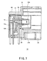
- a description of assembly of the circuit board connector 10 having the configuration described above is provided below referring to a lateral cross-sectional view (see Fig. 7 ) .
- the horizontal portions 22 of the plurality of terminals 12 are inserted into the insert holes 26 of the inner housing 14, and the plurality of terminals 12 are altogether housed in the inner housing 14.
- the inner housing 14 housing the plurality of terminals 12 is inserted into the shielding shell 16, and the back side of the inner housing 14 is covered with the shell cover 18.
- the shielding shell 16 housing the inner housing 14 is inserted into the housing portion 66 of the outer housing 20 from the back side, and accordingly, assembly is completed.
- the upper terminals 12a are located on the back side in the depth direction with respect to the lower terminals 12b when viewed from the width direction.
- the upper terminals 12a and the lower terminals 12b are arranged substantially parallel to each other, which prevents the circuit board connector 10 from becoming larger in the depth direction.
- the ends of the horizontal portions of the plurality of terminals 12 are arranged in two layers and three rows in the hood portion 62, and the tip portions of the vertical portions 24 protrude outside at positions directly below the rows and at a position slightly apart from the rows.
- the leg portions 40 of the shielding shell 16 protrude outside at side positions in the width direction of the vertical portions 24.
- the vertical portions 24 of the plurality of terminals 12 and the leg portions 40 of the shielding shell 16 that protrude from the lower end of the outer housing 20 are inserted into and soldered to the through holes connected to the printed wiring of the printed circuit board, by which the circuit board connector 10 is electrically connected to the printed wiring of the printed circuit board.
- the circuit board connector 10 is provided with the shielding shell 16 according to the preferred embodiments of the present invention, the circuit board connector 10 may not be provided with the shielding shell 16.
- the plurality of terminals 12 arranged in the width direction may not be arranged substantially parallel to each other and may be bent in the opposite directions, for example.
- the upper terminals 12a and the lower terminals 12b may not be arranged substantially parallel to each other when viewed from the width direction, if they do not intersect with each other.
Landscapes
- Coupling Device And Connection With Printed Circuit (AREA)
- Details Of Connecting Devices For Male And Female Coupling (AREA)
Claims (3)
- Connecteur (10) de carte de circuit imprimé comprenant :plusieurs bornes (12) comportant :des parties horizontales (22) conçues pour être connectées à des premières extrémités de fils électriques ; etdes parties verticales (24) s'étendant vers le bas depuis des premières extrémités des parties horizontales (22) et conçues pour être connectées à un motif de signal d'une carte de circuit imprimé,dans lequel les parties horizontales (22) des multiples bornes (12) sont agencées en une pluralité de couches dans une direction de hauteur, les parties verticales (24a) des bornes (12a) ayant les parties horizontales (22a) dans la couche supérieure sont situées sur un côté arrière dans une direction de profondeur par rapport aux parties verticales (24b) des bornes (12b) ayant les parties horizontales (22b) dans la couche inférieure, et les parties verticales (24b) des bornes (12b) dans la couche inférieure sont pliées dans le sens de la largeur,caractérisé en ce quelesdites parties verticales (24b) des bornes (12b) dans la couche inférieure sont pliées dans le sens de la largeur de manière à ce que la longueur de chemin des bornes (12a) dans la couche supérieure et une longueur de chemin des bornes (12b) dans la couche inférieure soient égales, etdans lequel les multiples bornes (12) sont logées dans un boîtier (14) comprenant plusieurs trous d'introduction (26) dans lesquels sont introduites les parties horizontales (22) des multiples bornes (12) etplusieurs rainures de réception (28) conçues pour recevoir les parties verticales (24) des multiples bornes (12), et les parties pointes des parties verticales pliées (24b) des bornes (12b) sont reçues par les rainures de réception (28) recevant les parties bases des parties verticales (24) des bornes adjacentes auxdites bornes (12b).
- Connecteur (10) de carte de circuit imprimé selon la revendication 1, dans lequel les multiples bornes (12) sont agencées de manière sensiblement parallèle les unes aux autres lorsqu'on les observe depuis le sens de la largeur.
- Connecteur (10) de carte de circuit imprimé selon l'une quelconque des revendications 1 et 2,
dans lequel les parties pointes des parties verticales pliées (24b) des bornes (12b) sont reçues par les rainures de réception (28) recevant les parties bases des parties verticales (24) des premières bornes adjacentes auxdites bornes (12).
Applications Claiming Priority (2)
| Application Number | Priority Date | Filing Date | Title |
|---|---|---|---|
| JP2007215538A JP5038818B2 (ja) | 2007-08-22 | 2007-08-22 | 基板用コネクタ |
| PCT/JP2008/064777 WO2009025276A1 (fr) | 2007-08-22 | 2008-08-20 | Connecteur de carte |
Publications (3)
| Publication Number | Publication Date |
|---|---|
| EP2184810A1 EP2184810A1 (fr) | 2010-05-12 |
| EP2184810A4 EP2184810A4 (fr) | 2012-04-18 |
| EP2184810B1 true EP2184810B1 (fr) | 2013-05-22 |
Family
ID=40378177
Family Applications (1)
| Application Number | Title | Priority Date | Filing Date |
|---|---|---|---|
| EP08827586.2A Not-in-force EP2184810B1 (fr) | 2007-08-22 | 2008-08-20 | Connecteur de carte |
Country Status (4)
| Country | Link |
|---|---|
| US (1) | US8083530B2 (fr) |
| EP (1) | EP2184810B1 (fr) |
| JP (1) | JP5038818B2 (fr) |
| WO (1) | WO2009025276A1 (fr) |
Families Citing this family (16)
| Publication number | Priority date | Publication date | Assignee | Title |
|---|---|---|---|---|
| JP5590991B2 (ja) * | 2010-06-30 | 2014-09-17 | 京セラコネクタプロダクツ株式会社 | コネクタ |
| JP2012142152A (ja) * | 2010-12-28 | 2012-07-26 | Tyco Electronics Japan Kk | 回路基板組立体、基板装置、回路基板組立体の組み立て方法 |
| US10081943B2 (en) * | 2012-07-31 | 2018-09-25 | Sumitomo (Sei) Steel Wire Corp. | Pregrouted PC steel material and method for hardening pregrout layer thereof |
| JP6054539B2 (ja) * | 2012-10-15 | 2016-12-27 | デルフィ・インターナショナル・オペレーションズ・ルクセンブルク・エス・アー・エール・エル | 電気コネクタ |
| JP6480719B2 (ja) * | 2013-12-25 | 2019-03-13 | 住友電工スチールワイヤー株式会社 | プレグラウトpc鋼材及びそのプレグラウト層の硬化方法 |
| WO2015164538A1 (fr) | 2014-04-23 | 2015-10-29 | Tyco Electronics Corporation | Connecteur électrique à capuchon de protection et à bornes protégées |
| US9525246B2 (en) * | 2014-05-05 | 2016-12-20 | Tyco Electronics Corporation | Printed circuit board connector assembly having contact shield with integral securing members |
| US9899780B2 (en) * | 2015-07-15 | 2018-02-20 | Alan L. Pocrass | RJ and USB connectors with grooved contact pins |
| JP6534917B2 (ja) * | 2015-11-26 | 2019-06-26 | 日本圧着端子製造株式会社 | シールドコネクタ |
| JP2017224472A (ja) * | 2016-06-15 | 2017-12-21 | 株式会社オートネットワーク技術研究所 | 基板用コネクタ |
| US10939546B2 (en) * | 2019-01-28 | 2021-03-02 | Eagle Technology, Llc | Interconnect device |
| JP6879648B2 (ja) * | 2019-02-27 | 2021-06-02 | 住友電装株式会社 | 外導体端子及びシールドコネクタ |
| JP2020173988A (ja) * | 2019-04-11 | 2020-10-22 | 矢崎総業株式会社 | イーサネット用端子 |
| CN110829083A (zh) * | 2019-11-05 | 2020-02-21 | 富加宜连接器(东莞)有限公司 | 一种防串扰的高速连接器 |
| DE102020119282B4 (de) | 2020-07-22 | 2022-06-09 | Md Elektronik Gmbh | Kontaktvorrichtung |
| DE102021107810A1 (de) * | 2021-03-29 | 2022-09-29 | Md Elektronik Gmbh | Platinenstecker |
Family Cites Families (20)
| Publication number | Priority date | Publication date | Assignee | Title |
|---|---|---|---|---|
| US4802860A (en) * | 1987-03-04 | 1989-02-07 | Hirose Electric Co., Ltd. | Surface mount type electrical connector |
| JP2711910B2 (ja) | 1989-08-31 | 1998-02-10 | マルマス機械株式会社 | 粒状物の色彩選別装置 |
| JP3070165B2 (ja) | 1991-08-09 | 2000-07-24 | 松下電器産業株式会社 | 洗濯機の布量検知装置 |
| US5273460A (en) | 1991-09-17 | 1993-12-28 | Hosiden Corporation | Electrical parts for surface mounting |
| JP2549998Y2 (ja) * | 1991-10-07 | 1997-10-08 | モレックス インコーポレーテッド | 電気コネクタ |
| JPH069068A (ja) | 1992-06-24 | 1994-01-18 | Canon Inc | 画像形成装置 |
| JP2769965B2 (ja) * | 1993-07-19 | 1998-06-25 | 日本圧着端子製造株式会社 | 表面実装コネクタ |
| JP2848762B2 (ja) | 1993-07-26 | 1999-01-20 | 三菱電機株式会社 | データ授受システムおよびその方法 |
| US5453016A (en) * | 1993-11-15 | 1995-09-26 | Berg Technology, Inc. | Right angle electrical connector and insertion tool therefor |
| JP2598650Y2 (ja) | 1993-12-14 | 1999-08-16 | モレックス インコーポレーテッド | プリント回路基板接続用電気コネクタ |
| JP2000012130A (ja) * | 1998-06-26 | 2000-01-14 | Nec Corp | コネクタ構造 |
| JP2000068006A (ja) | 1998-08-20 | 2000-03-03 | Fujitsu Takamisawa Component Ltd | ライトアングル型コネクタ |
| TW543962U (en) | 2002-08-30 | 2003-07-21 | Molex Inc | Electrical connector |
| TW572416U (en) * | 2002-11-15 | 2004-01-11 | Hon Hai Prec Ind Co Ltd | Stacked electrical connector |
| JP4212956B2 (ja) * | 2003-05-27 | 2009-01-21 | 富士通コンポーネント株式会社 | 平衡伝送用コネクタ |
| JP4212955B2 (ja) * | 2003-05-27 | 2009-01-21 | 富士通コンポーネント株式会社 | 平衡伝送用プラグコネクタ |
| US7500871B2 (en) * | 2006-08-21 | 2009-03-10 | Fci Americas Technology, Inc. | Electrical connector system with jogged contact tails |
| US7841894B2 (en) * | 2008-04-28 | 2010-11-30 | Hon Hai Precision Ind. Co., Ltd. | Stacked electronical connector |
| JP4647675B2 (ja) * | 2008-07-22 | 2011-03-09 | ホシデン株式会社 | コネクタ |
| US7972151B2 (en) * | 2009-01-05 | 2011-07-05 | Hon Hai Precision Ind. Co., Ltd. | Electrical connector with improved arrangement of ground and signal contacts |
-
2007
- 2007-08-22 JP JP2007215538A patent/JP5038818B2/ja not_active Expired - Fee Related
-
2008
- 2008-08-20 US US12/674,321 patent/US8083530B2/en not_active Expired - Fee Related
- 2008-08-20 EP EP08827586.2A patent/EP2184810B1/fr not_active Not-in-force
- 2008-08-20 WO PCT/JP2008/064777 patent/WO2009025276A1/fr active Application Filing
Also Published As
| Publication number | Publication date |
|---|---|
| US20110151722A1 (en) | 2011-06-23 |
| EP2184810A1 (fr) | 2010-05-12 |
| WO2009025276A1 (fr) | 2009-02-26 |
| US8083530B2 (en) | 2011-12-27 |
| JP5038818B2 (ja) | 2012-10-03 |
| EP2184810A4 (fr) | 2012-04-18 |
| JP2009048919A (ja) | 2009-03-05 |
Similar Documents
| Publication | Publication Date | Title |
|---|---|---|
| EP2184810B1 (fr) | Connecteur de carte | |
| US11011874B2 (en) | Connector and connector assembly | |
| US10320126B2 (en) | Electrical connector and electrical connector assembly | |
| CN101350480B (zh) | 电连接器 | |
| JP5197742B2 (ja) | 電気コネクタ | |
| US6705902B1 (en) | Connector assembly having contacts with uniform electrical property of resistance | |
| CA2550486C (fr) | Connecteur de carte imprimee pour transmission de signaux differentiels | |
| US9257797B2 (en) | Cable assembly having an improved circuit board | |
| JP2005079093A (ja) | 電気コネクタ | |
| US20080261462A1 (en) | Board-to-Board Connector | |
| JP3134262U (ja) | 表面実装型コネクタ | |
| US11444414B2 (en) | Connector and connector device | |
| CN101557055B (zh) | 屏蔽壳及基板组件 | |
| US11664628B2 (en) | Electrical connector with shielding between low and high frequency terminals and electrical connector device using the same | |
| US20090227138A1 (en) | Electrical connector adapter for connecting with two rows of cables | |
| US6739915B1 (en) | Electrical connector with rear retention mechanism of outer shell | |
| CN110086018B (zh) | 电连接器 | |
| CN103078209B (zh) | 连接器 | |
| US9685741B2 (en) | Cable connector assembly with improved metal shell | |
| TWI689137B (zh) | 用於高速信號傳輸的連接器 | |
| JP5549072B2 (ja) | 回路基板内蔵コネクタ | |
| CN117813732A (zh) | 包括插座连接器和插头连接器的连接器组件及插头连接器 | |
| JP5473638B2 (ja) | 電気コネクタ | |
| US20060228942A1 (en) | Fine wire coaxial connector | |
| JP2009004117A (ja) | 多極コネクタ |
Legal Events
| Date | Code | Title | Description |
|---|---|---|---|
| PUAI | Public reference made under article 153(3) epc to a published international application that has entered the european phase |
Free format text: ORIGINAL CODE: 0009012 |
|
| 17P | Request for examination filed |
Effective date: 20100226 |
|
| AK | Designated contracting states |
Kind code of ref document: A1 Designated state(s): AT BE BG CH CY CZ DE DK EE ES FI FR GB GR HR HU IE IS IT LI LT LU LV MC MT NL NO PL PT RO SE SI SK TR |
|
| AX | Request for extension of the european patent |
Extension state: AL BA MK RS |
|
| DAX | Request for extension of the european patent (deleted) | ||
| REG | Reference to a national code |
Ref country code: DE Ref legal event code: R079 Ref document number: 602008024857 Country of ref document: DE Free format text: PREVIOUS MAIN CLASS: H01R0012160000 Ipc: H01R0013658000 |
|
| A4 | Supplementary search report drawn up and despatched |
Effective date: 20120316 |
|
| RIC1 | Information provided on ipc code assigned before grant |
Ipc: H01R 24/00 20110101ALI20120316BHEP Ipc: H01R 13/658 20110101AFI20120316BHEP |
|
| GRAP | Despatch of communication of intention to grant a patent |
Free format text: ORIGINAL CODE: EPIDOSNIGR1 |
|
| GRAS | Grant fee paid |
Free format text: ORIGINAL CODE: EPIDOSNIGR3 |
|
| GRAA | (expected) grant |
Free format text: ORIGINAL CODE: 0009210 |
|
| AK | Designated contracting states |
Kind code of ref document: B1 Designated state(s): AT BE BG CH CY CZ DE DK EE ES FI FR GB GR HR HU IE IS IT LI LT LU LV MC MT NL NO PL PT RO SE SI SK TR |
|
| REG | Reference to a national code |
Ref country code: GB Ref legal event code: FG4D |
|
| REG | Reference to a national code |
Ref country code: CH Ref legal event code: EP |
|
| REG | Reference to a national code |
Ref country code: AT Ref legal event code: REF Ref document number: 613653 Country of ref document: AT Kind code of ref document: T Effective date: 20130615 |
|
| REG | Reference to a national code |
Ref country code: IE Ref legal event code: FG4D |
|
| REG | Reference to a national code |
Ref country code: DE Ref legal event code: R096 Ref document number: 602008024857 Country of ref document: DE Effective date: 20130718 |
|
| REG | Reference to a national code |
Ref country code: AT Ref legal event code: MK05 Ref document number: 613653 Country of ref document: AT Kind code of ref document: T Effective date: 20130522 |
|
| REG | Reference to a national code |
Ref country code: LT Ref legal event code: MG4D |
|
| PG25 | Lapsed in a contracting state [announced via postgrant information from national office to epo] |
Ref country code: SI Free format text: LAPSE BECAUSE OF FAILURE TO SUBMIT A TRANSLATION OF THE DESCRIPTION OR TO PAY THE FEE WITHIN THE PRESCRIBED TIME-LIMIT Effective date: 20130522 Ref country code: FI Free format text: LAPSE BECAUSE OF FAILURE TO SUBMIT A TRANSLATION OF THE DESCRIPTION OR TO PAY THE FEE WITHIN THE PRESCRIBED TIME-LIMIT Effective date: 20130522 Ref country code: AT Free format text: LAPSE BECAUSE OF FAILURE TO SUBMIT A TRANSLATION OF THE DESCRIPTION OR TO PAY THE FEE WITHIN THE PRESCRIBED TIME-LIMIT Effective date: 20130522 Ref country code: IS Free format text: LAPSE BECAUSE OF FAILURE TO SUBMIT A TRANSLATION OF THE DESCRIPTION OR TO PAY THE FEE WITHIN THE PRESCRIBED TIME-LIMIT Effective date: 20130922 Ref country code: PT Free format text: LAPSE BECAUSE OF FAILURE TO SUBMIT A TRANSLATION OF THE DESCRIPTION OR TO PAY THE FEE WITHIN THE PRESCRIBED TIME-LIMIT Effective date: 20130923 Ref country code: ES Free format text: LAPSE BECAUSE OF FAILURE TO SUBMIT A TRANSLATION OF THE DESCRIPTION OR TO PAY THE FEE WITHIN THE PRESCRIBED TIME-LIMIT Effective date: 20130902 Ref country code: GR Free format text: LAPSE BECAUSE OF FAILURE TO SUBMIT A TRANSLATION OF THE DESCRIPTION OR TO PAY THE FEE WITHIN THE PRESCRIBED TIME-LIMIT Effective date: 20130823 Ref country code: SE Free format text: LAPSE BECAUSE OF FAILURE TO SUBMIT A TRANSLATION OF THE DESCRIPTION OR TO PAY THE FEE WITHIN THE PRESCRIBED TIME-LIMIT Effective date: 20130522 Ref country code: NO Free format text: LAPSE BECAUSE OF FAILURE TO SUBMIT A TRANSLATION OF THE DESCRIPTION OR TO PAY THE FEE WITHIN THE PRESCRIBED TIME-LIMIT Effective date: 20130822 Ref country code: LT Free format text: LAPSE BECAUSE OF FAILURE TO SUBMIT A TRANSLATION OF THE DESCRIPTION OR TO PAY THE FEE WITHIN THE PRESCRIBED TIME-LIMIT Effective date: 20130522 |
|
| REG | Reference to a national code |
Ref country code: NL Ref legal event code: VDEP Effective date: 20130522 |
|
| PG25 | Lapsed in a contracting state [announced via postgrant information from national office to epo] |
Ref country code: HR Free format text: LAPSE BECAUSE OF FAILURE TO SUBMIT A TRANSLATION OF THE DESCRIPTION OR TO PAY THE FEE WITHIN THE PRESCRIBED TIME-LIMIT Effective date: 20130522 Ref country code: BG Free format text: LAPSE BECAUSE OF FAILURE TO SUBMIT A TRANSLATION OF THE DESCRIPTION OR TO PAY THE FEE WITHIN THE PRESCRIBED TIME-LIMIT Effective date: 20130822 Ref country code: PL Free format text: LAPSE BECAUSE OF FAILURE TO SUBMIT A TRANSLATION OF THE DESCRIPTION OR TO PAY THE FEE WITHIN THE PRESCRIBED TIME-LIMIT Effective date: 20130522 |
|
| PG25 | Lapsed in a contracting state [announced via postgrant information from national office to epo] |
Ref country code: LV Free format text: LAPSE BECAUSE OF FAILURE TO SUBMIT A TRANSLATION OF THE DESCRIPTION OR TO PAY THE FEE WITHIN THE PRESCRIBED TIME-LIMIT Effective date: 20130522 |
|
| PG25 | Lapsed in a contracting state [announced via postgrant information from national office to epo] |
Ref country code: BE Free format text: LAPSE BECAUSE OF FAILURE TO SUBMIT A TRANSLATION OF THE DESCRIPTION OR TO PAY THE FEE WITHIN THE PRESCRIBED TIME-LIMIT Effective date: 20130522 Ref country code: CZ Free format text: LAPSE BECAUSE OF FAILURE TO SUBMIT A TRANSLATION OF THE DESCRIPTION OR TO PAY THE FEE WITHIN THE PRESCRIBED TIME-LIMIT Effective date: 20130522 Ref country code: DK Free format text: LAPSE BECAUSE OF FAILURE TO SUBMIT A TRANSLATION OF THE DESCRIPTION OR TO PAY THE FEE WITHIN THE PRESCRIBED TIME-LIMIT Effective date: 20130522 Ref country code: SK Free format text: LAPSE BECAUSE OF FAILURE TO SUBMIT A TRANSLATION OF THE DESCRIPTION OR TO PAY THE FEE WITHIN THE PRESCRIBED TIME-LIMIT Effective date: 20130522 Ref country code: EE Free format text: LAPSE BECAUSE OF FAILURE TO SUBMIT A TRANSLATION OF THE DESCRIPTION OR TO PAY THE FEE WITHIN THE PRESCRIBED TIME-LIMIT Effective date: 20130522 |
|
| PG25 | Lapsed in a contracting state [announced via postgrant information from national office to epo] |
Ref country code: NL Free format text: LAPSE BECAUSE OF FAILURE TO SUBMIT A TRANSLATION OF THE DESCRIPTION OR TO PAY THE FEE WITHIN THE PRESCRIBED TIME-LIMIT Effective date: 20130522 Ref country code: RO Free format text: LAPSE BECAUSE OF FAILURE TO SUBMIT A TRANSLATION OF THE DESCRIPTION OR TO PAY THE FEE WITHIN THE PRESCRIBED TIME-LIMIT Effective date: 20130522 Ref country code: IT Free format text: LAPSE BECAUSE OF FAILURE TO SUBMIT A TRANSLATION OF THE DESCRIPTION OR TO PAY THE FEE WITHIN THE PRESCRIBED TIME-LIMIT Effective date: 20130522 |
|
| PLBE | No opposition filed within time limit |
Free format text: ORIGINAL CODE: 0009261 |
|
| STAA | Information on the status of an ep patent application or granted ep patent |
Free format text: STATUS: NO OPPOSITION FILED WITHIN TIME LIMIT |
|
| REG | Reference to a national code |
Ref country code: CH Ref legal event code: PL |
|
| GBPC | Gb: european patent ceased through non-payment of renewal fee |
Effective date: 20130822 |
|
| 26N | No opposition filed |
Effective date: 20140225 |
|
| PG25 | Lapsed in a contracting state [announced via postgrant information from national office to epo] |
Ref country code: DE Free format text: LAPSE BECAUSE OF NON-PAYMENT OF DUE FEES Effective date: 20140301 Ref country code: LI Free format text: LAPSE BECAUSE OF NON-PAYMENT OF DUE FEES Effective date: 20130831 Ref country code: CH Free format text: LAPSE BECAUSE OF NON-PAYMENT OF DUE FEES Effective date: 20130831 Ref country code: MC Free format text: LAPSE BECAUSE OF FAILURE TO SUBMIT A TRANSLATION OF THE DESCRIPTION OR TO PAY THE FEE WITHIN THE PRESCRIBED TIME-LIMIT Effective date: 20130522 |
|
| REG | Reference to a national code |
Ref country code: IE Ref legal event code: MM4A |
|
| REG | Reference to a national code |
Ref country code: DE Ref legal event code: R119 Ref document number: 602008024857 Country of ref document: DE Effective date: 20140301 |
|
| REG | Reference to a national code |
Ref country code: FR Ref legal event code: ST Effective date: 20140430 |
|
| REG | Reference to a national code |
Ref country code: DE Ref legal event code: R097 Ref document number: 602008024857 Country of ref document: DE Effective date: 20140225 |
|
| PG25 | Lapsed in a contracting state [announced via postgrant information from national office to epo] |
Ref country code: IE Free format text: LAPSE BECAUSE OF NON-PAYMENT OF DUE FEES Effective date: 20130820 Ref country code: GB Free format text: LAPSE BECAUSE OF NON-PAYMENT OF DUE FEES Effective date: 20130822 |
|
| PG25 | Lapsed in a contracting state [announced via postgrant information from national office to epo] |
Ref country code: FR Free format text: LAPSE BECAUSE OF NON-PAYMENT OF DUE FEES Effective date: 20130902 |
|
| PG25 | Lapsed in a contracting state [announced via postgrant information from national office to epo] |
Ref country code: MT Free format text: LAPSE BECAUSE OF FAILURE TO SUBMIT A TRANSLATION OF THE DESCRIPTION OR TO PAY THE FEE WITHIN THE PRESCRIBED TIME-LIMIT Effective date: 20130522 Ref country code: TR Free format text: LAPSE BECAUSE OF FAILURE TO SUBMIT A TRANSLATION OF THE DESCRIPTION OR TO PAY THE FEE WITHIN THE PRESCRIBED TIME-LIMIT Effective date: 20130522 Ref country code: CY Free format text: LAPSE BECAUSE OF FAILURE TO SUBMIT A TRANSLATION OF THE DESCRIPTION OR TO PAY THE FEE WITHIN THE PRESCRIBED TIME-LIMIT Effective date: 20130522 |
|
| PG25 | Lapsed in a contracting state [announced via postgrant information from national office to epo] |
Ref country code: HU Free format text: LAPSE BECAUSE OF FAILURE TO SUBMIT A TRANSLATION OF THE DESCRIPTION OR TO PAY THE FEE WITHIN THE PRESCRIBED TIME-LIMIT; INVALID AB INITIO Effective date: 20080820 Ref country code: LU Free format text: LAPSE BECAUSE OF NON-PAYMENT OF DUE FEES Effective date: 20130820 |