EP2178894B1 - Metallorganische vorstufen zur verwendung bei abscheidungsverfahren in der chemischen phase - Google Patents
Metallorganische vorstufen zur verwendung bei abscheidungsverfahren in der chemischen phase Download PDFInfo
- Publication number
- EP2178894B1 EP2178894B1 EP08782322.5A EP08782322A EP2178894B1 EP 2178894 B1 EP2178894 B1 EP 2178894B1 EP 08782322 A EP08782322 A EP 08782322A EP 2178894 B1 EP2178894 B1 EP 2178894B1
- Authority
- EP
- European Patent Office
- Prior art keywords
- propyl
- dicarbonyl
- ruthenium
- ethyl
- methyl
- Prior art date
- Legal status (The legal status is an assumption and is not a legal conclusion. Google has not performed a legal analysis and makes no representation as to the accuracy of the status listed.)
- Not-in-force
Links
- 125000002524 organometallic group Chemical group 0.000 title claims description 26
- 239000002243 precursor Substances 0.000 title description 77
- 239000000126 substance Substances 0.000 title description 10
- 238000005137 deposition process Methods 0.000 title description 8
- 125000002496 methyl group Chemical group [H]C([H])([H])* 0.000 claims description 135
- -1 methylcyclopentadienyl Chemical group 0.000 claims description 81
- 229910052707 ruthenium Inorganic materials 0.000 claims description 78
- KJTLSVCANCCWHF-UHFFFAOYSA-N Ruthenium Chemical compound [Ru] KJTLSVCANCCWHF-UHFFFAOYSA-N 0.000 claims description 70
- 125000004989 dicarbonyl group Chemical group 0.000 claims description 68
- 125000001495 ethyl group Chemical group [H]C([H])([H])C([H])([H])* 0.000 claims description 65
- 125000001436 propyl group Chemical group [H]C([*])([H])C([H])([H])C([H])([H])[H] 0.000 claims description 48
- 125000000484 butyl group Chemical group [H]C([*])([H])C([H])([H])C([H])([H])C([H])([H])[H] 0.000 claims description 36
- 229910052762 osmium Inorganic materials 0.000 claims description 35
- SYQBFIAQOQZEGI-UHFFFAOYSA-N osmium atom Chemical compound [Os] SYQBFIAQOQZEGI-UHFFFAOYSA-N 0.000 claims description 28
- 125000000008 (C1-C10) alkyl group Chemical group 0.000 claims description 12
- 125000000959 isobutyl group Chemical group [H]C([H])([H])C([H])(C([H])([H])[H])C([H])([H])* 0.000 claims description 3
- 125000001449 isopropyl group Chemical group [H]C([H])([H])C([H])(*)C([H])([H])[H] 0.000 claims description 3
- 125000004108 n-butyl group Chemical group [H]C([H])([H])C([H])([H])C([H])([H])C([H])([H])* 0.000 claims description 3
- 125000004123 n-propyl group Chemical group [H]C([H])([H])C([H])([H])C([H])([H])* 0.000 claims description 3
- 125000002914 sec-butyl group Chemical group [H]C([H])([H])C([H])([H])C([H])(*)C([H])([H])[H] 0.000 claims description 3
- 125000000999 tert-butyl group Chemical group [H]C([H])([H])C(*)(C([H])([H])[H])C([H])([H])[H] 0.000 claims description 3
- 238000000231 atomic layer deposition Methods 0.000 description 59
- 239000010408 film Substances 0.000 description 28
- 238000000034 method Methods 0.000 description 28
- 229910052751 metal Inorganic materials 0.000 description 25
- 239000000758 substrate Substances 0.000 description 25
- 238000005229 chemical vapour deposition Methods 0.000 description 23
- ZSWFCLXCOIISFI-UHFFFAOYSA-N cyclopentadiene Chemical class C1C=CC=C1 ZSWFCLXCOIISFI-UHFFFAOYSA-N 0.000 description 23
- 239000002184 metal Substances 0.000 description 23
- 238000002347 injection Methods 0.000 description 21
- 239000007924 injection Substances 0.000 description 21
- VLKZOEOYAKHREP-UHFFFAOYSA-N n-Hexane Chemical compound CCCCCC VLKZOEOYAKHREP-UHFFFAOYSA-N 0.000 description 21
- 125000000058 cyclopentadienyl group Chemical group C1(=CC=CC1)* 0.000 description 19
- XKRFYHLGVUSROY-UHFFFAOYSA-N Argon Chemical compound [Ar] XKRFYHLGVUSROY-UHFFFAOYSA-N 0.000 description 18
- IJGRMHOSHXDMSA-UHFFFAOYSA-N Atomic nitrogen Chemical compound N#N IJGRMHOSHXDMSA-UHFFFAOYSA-N 0.000 description 18
- 239000010409 thin film Substances 0.000 description 16
- YXFVVABEGXRONW-UHFFFAOYSA-N Toluene Chemical compound CC1=CC=CC=C1 YXFVVABEGXRONW-UHFFFAOYSA-N 0.000 description 15
- 239000000243 solution Substances 0.000 description 14
- 239000003708 ampul Substances 0.000 description 12
- 238000006243 chemical reaction Methods 0.000 description 11
- 238000000151 deposition Methods 0.000 description 11
- 230000008021 deposition Effects 0.000 description 11
- 238000010926 purge Methods 0.000 description 11
- 239000002904 solvent Substances 0.000 description 11
- 238000002411 thermogravimetry Methods 0.000 description 10
- 125000000217 alkyl group Chemical group 0.000 description 9
- 229910052786 argon Inorganic materials 0.000 description 9
- 230000015572 biosynthetic process Effects 0.000 description 9
- 229910052757 nitrogen Inorganic materials 0.000 description 9
- 239000007788 liquid Substances 0.000 description 8
- 238000003786 synthesis reaction Methods 0.000 description 8
- OKTJSMMVPCPJKN-UHFFFAOYSA-N Carbon Chemical compound [C] OKTJSMMVPCPJKN-UHFFFAOYSA-N 0.000 description 7
- IMNFDUFMRHMDMM-UHFFFAOYSA-N N-Heptane Chemical compound CCCCCCC IMNFDUFMRHMDMM-UHFFFAOYSA-N 0.000 description 6
- 229910052799 carbon Inorganic materials 0.000 description 6
- NQZFAUXPNWSLBI-UHFFFAOYSA-N carbon monoxide;ruthenium Chemical compound [Ru].[Ru].[Ru].[O+]#[C-].[O+]#[C-].[O+]#[C-].[O+]#[C-].[O+]#[C-].[O+]#[C-].[O+]#[C-].[O+]#[C-].[O+]#[C-].[O+]#[C-].[O+]#[C-].[O+]#[C-] NQZFAUXPNWSLBI-UHFFFAOYSA-N 0.000 description 6
- 239000001257 hydrogen Substances 0.000 description 6
- 229910052739 hydrogen Inorganic materials 0.000 description 6
- UFHFLCQGNIYNRP-UHFFFAOYSA-N Hydrogen Chemical compound [H][H] UFHFLCQGNIYNRP-UHFFFAOYSA-N 0.000 description 5
- QVGXLLKOCUKJST-UHFFFAOYSA-N atomic oxygen Chemical compound [O] QVGXLLKOCUKJST-UHFFFAOYSA-N 0.000 description 5
- 239000001301 oxygen Substances 0.000 description 5
- 229910052760 oxygen Inorganic materials 0.000 description 5
- 238000004833 X-ray photoelectron spectroscopy Methods 0.000 description 4
- 239000003446 ligand Substances 0.000 description 4
- AMXOYNBUYSYVKV-UHFFFAOYSA-M lithium bromide Chemical compound [Li+].[Br-] AMXOYNBUYSYVKV-UHFFFAOYSA-M 0.000 description 4
- 229910044991 metal oxide Inorganic materials 0.000 description 4
- 150000004706 metal oxides Chemical class 0.000 description 4
- 239000003921 oil Substances 0.000 description 4
- 238000001878 scanning electron micrograph Methods 0.000 description 4
- 239000004065 semiconductor Substances 0.000 description 4
- 229910001220 stainless steel Inorganic materials 0.000 description 4
- 239000010935 stainless steel Substances 0.000 description 4
- UHOVQNZJYSORNB-UHFFFAOYSA-N Benzene Chemical compound C1=CC=CC=C1 UHOVQNZJYSORNB-UHFFFAOYSA-N 0.000 description 3
- MZRVEZGGRBJDDB-UHFFFAOYSA-N N-Butyllithium Chemical compound [Li]CCCC MZRVEZGGRBJDDB-UHFFFAOYSA-N 0.000 description 3
- VYPSYNLAJGMNEJ-UHFFFAOYSA-N Silicium dioxide Chemical compound O=[Si]=O VYPSYNLAJGMNEJ-UHFFFAOYSA-N 0.000 description 3
- XUIMIQQOPSSXEZ-UHFFFAOYSA-N Silicon Chemical compound [Si] XUIMIQQOPSSXEZ-UHFFFAOYSA-N 0.000 description 3
- 150000001875 compounds Chemical class 0.000 description 3
- 239000010949 copper Substances 0.000 description 3
- 230000000694 effects Effects 0.000 description 3
- 150000002430 hydrocarbons Chemical class 0.000 description 3
- 229910052742 iron Inorganic materials 0.000 description 3
- 239000000203 mixture Substances 0.000 description 3
- 229910052710 silicon Inorganic materials 0.000 description 3
- 239000010703 silicon Substances 0.000 description 3
- 239000007787 solid Substances 0.000 description 3
- MZLGASXMSKOWSE-UHFFFAOYSA-N tantalum nitride Chemical compound [Ta]#N MZLGASXMSKOWSE-UHFFFAOYSA-N 0.000 description 3
- XLYOFNOQVPJJNP-UHFFFAOYSA-N water Substances O XLYOFNOQVPJJNP-UHFFFAOYSA-N 0.000 description 3
- QGZKDVFQNNGYKY-UHFFFAOYSA-N Ammonia Chemical compound N QGZKDVFQNNGYKY-UHFFFAOYSA-N 0.000 description 2
- 239000004215 Carbon black (E152) Substances 0.000 description 2
- YMWUJEATGCHHMB-UHFFFAOYSA-N Dichloromethane Chemical compound ClCCl YMWUJEATGCHHMB-UHFFFAOYSA-N 0.000 description 2
- OAKJQQAXSVQMHS-UHFFFAOYSA-N Hydrazine Chemical compound NN OAKJQQAXSVQMHS-UHFFFAOYSA-N 0.000 description 2
- CBENFWSGALASAD-UHFFFAOYSA-N Ozone Chemical compound [O-][O+]=O CBENFWSGALASAD-UHFFFAOYSA-N 0.000 description 2
- OFBQJSOFQDEBGM-UHFFFAOYSA-N Pentane Chemical compound CCCCC OFBQJSOFQDEBGM-UHFFFAOYSA-N 0.000 description 2
- HEDRZPFGACZZDS-MICDWDOJSA-N Trichloro(2H)methane Chemical compound [2H]C(Cl)(Cl)Cl HEDRZPFGACZZDS-MICDWDOJSA-N 0.000 description 2
- FCIBCALVQNVXGB-UHFFFAOYSA-N [Ru].[CH]1C=CC=C1 Chemical compound [Ru].[CH]1C=CC=C1 FCIBCALVQNVXGB-UHFFFAOYSA-N 0.000 description 2
- 239000000853 adhesive Substances 0.000 description 2
- 230000001070 adhesive effect Effects 0.000 description 2
- 150000001412 amines Chemical class 0.000 description 2
- 230000004888 barrier function Effects 0.000 description 2
- UHOVQNZJYSORNB-MZWXYZOWSA-N benzene-d6 Chemical compound [2H]C1=C([2H])C([2H])=C([2H])C([2H])=C1[2H] UHOVQNZJYSORNB-MZWXYZOWSA-N 0.000 description 2
- AXYSDZQJEIAXBL-UHFFFAOYSA-N bis(oxomethylidene)iron Chemical compound O=C=[Fe]=C=O AXYSDZQJEIAXBL-UHFFFAOYSA-N 0.000 description 2
- UORVGPXVDQYIDP-UHFFFAOYSA-N borane Chemical compound B UORVGPXVDQYIDP-UHFFFAOYSA-N 0.000 description 2
- 239000003990 capacitor Substances 0.000 description 2
- 125000004432 carbon atom Chemical group C* 0.000 description 2
- UUZRATKFAUQBJJ-UHFFFAOYSA-N carbon monoxide;iron Chemical compound [Fe].[O+]#[C-].[O+]#[C-].[O+]#[C-] UUZRATKFAUQBJJ-UHFFFAOYSA-N 0.000 description 2
- 239000003054 catalyst Substances 0.000 description 2
- 238000012512 characterization method Methods 0.000 description 2
- 238000001311 chemical methods and process Methods 0.000 description 2
- 238000003776 cleavage reaction Methods 0.000 description 2
- 229910052802 copper Inorganic materials 0.000 description 2
- 239000002178 crystalline material Substances 0.000 description 2
- 238000009792 diffusion process Methods 0.000 description 2
- ZMMJGEGLRURXTF-UHFFFAOYSA-N ethidium bromide Chemical compound [Br-].C12=CC(N)=CC=C2C2=CC=C(N)C=C2[N+](CC)=C1C1=CC=CC=C1 ZMMJGEGLRURXTF-UHFFFAOYSA-N 0.000 description 2
- 238000001704 evaporation Methods 0.000 description 2
- 230000008020 evaporation Effects 0.000 description 2
- 239000007789 gas Substances 0.000 description 2
- 229930195733 hydrocarbon Natural products 0.000 description 2
- 238000011835 investigation Methods 0.000 description 2
- 239000010410 layer Substances 0.000 description 2
- BKIMMITUMNQMOS-UHFFFAOYSA-N nonane Chemical compound CCCCCCCCC BKIMMITUMNQMOS-UHFFFAOYSA-N 0.000 description 2
- 239000000376 reactant Substances 0.000 description 2
- 239000002356 single layer Substances 0.000 description 2
- 125000001424 substituent group Chemical group 0.000 description 2
- 230000003746 surface roughness Effects 0.000 description 2
- 229910052723 transition metal Inorganic materials 0.000 description 2
- 150000003624 transition metals Chemical class 0.000 description 2
- RIOQSEWOXXDEQQ-UHFFFAOYSA-N triphenylphosphine Chemical compound C1=CC=CC=C1P(C=1C=CC=CC=1)C1=CC=CC=C1 RIOQSEWOXXDEQQ-UHFFFAOYSA-N 0.000 description 2
- 238000004009 13C{1H}-NMR spectroscopy Methods 0.000 description 1
- 238000005160 1H NMR spectroscopy Methods 0.000 description 1
- CPELXLSAUQHCOX-UHFFFAOYSA-M Bromide Chemical compound [Br-] CPELXLSAUQHCOX-UHFFFAOYSA-M 0.000 description 1
- 229920000049 Carbon (fiber) Polymers 0.000 description 1
- RYGMFSIKBFXOCR-UHFFFAOYSA-N Copper Chemical compound [Cu] RYGMFSIKBFXOCR-UHFFFAOYSA-N 0.000 description 1
- 238000005481 NMR spectroscopy Methods 0.000 description 1
- CTQNGGLPUBDAKN-UHFFFAOYSA-N O-Xylene Chemical compound CC1=CC=CC=C1C CTQNGGLPUBDAKN-UHFFFAOYSA-N 0.000 description 1
- ZLMJMSJWJFRBEC-UHFFFAOYSA-N Potassium Chemical class [K] ZLMJMSJWJFRBEC-UHFFFAOYSA-N 0.000 description 1
- 239000012327 Ruthenium complex Substances 0.000 description 1
- 229910052581 Si3N4 Inorganic materials 0.000 description 1
- BLRPTPMANUNPDV-UHFFFAOYSA-N Silane Chemical compound [SiH4] BLRPTPMANUNPDV-UHFFFAOYSA-N 0.000 description 1
- OCBFFGCSTGGPSQ-UHFFFAOYSA-N [CH2]CC Chemical group [CH2]CC OCBFFGCSTGGPSQ-UHFFFAOYSA-N 0.000 description 1
- YNRYSMYFGAZUAU-UHFFFAOYSA-N [C].[Os] Chemical compound [C].[Os] YNRYSMYFGAZUAU-UHFFFAOYSA-N 0.000 description 1
- QVYYOKWPCQYKEY-UHFFFAOYSA-N [Fe].[Co] Chemical compound [Fe].[Co] QVYYOKWPCQYKEY-UHFFFAOYSA-N 0.000 description 1
- 239000003570 air Substances 0.000 description 1
- 125000001931 aliphatic group Chemical group 0.000 description 1
- 150000001338 aliphatic hydrocarbons Chemical class 0.000 description 1
- 229910021529 ammonia Inorganic materials 0.000 description 1
- 150000004945 aromatic hydrocarbons Chemical class 0.000 description 1
- 238000003877 atomic layer epitaxy Methods 0.000 description 1
- 238000009835 boiling Methods 0.000 description 1
- 229910000085 borane Inorganic materials 0.000 description 1
- RDHPKYGYEGBMSE-UHFFFAOYSA-N bromoethane Chemical compound CCBr RDHPKYGYEGBMSE-UHFFFAOYSA-N 0.000 description 1
- 239000006227 byproduct Substances 0.000 description 1
- 238000004364 calculation method Methods 0.000 description 1
- 239000004917 carbon fiber Substances 0.000 description 1
- 239000011203 carbon fibre reinforced carbon Substances 0.000 description 1
- 239000002041 carbon nanotube Substances 0.000 description 1
- 229910021393 carbon nanotube Inorganic materials 0.000 description 1
- 238000005234 chemical deposition Methods 0.000 description 1
- 239000003638 chemical reducing agent Substances 0.000 description 1
- 229910052681 coesite Inorganic materials 0.000 description 1
- 230000000295 complement effect Effects 0.000 description 1
- 238000001816 cooling Methods 0.000 description 1
- 229910052906 cristobalite Inorganic materials 0.000 description 1
- 239000013078 crystal Substances 0.000 description 1
- 150000004292 cyclic ethers Chemical class 0.000 description 1
- SBZXBUIDTXKZTM-UHFFFAOYSA-N diglyme Chemical compound COCCOCCOC SBZXBUIDTXKZTM-UHFFFAOYSA-N 0.000 description 1
- 239000000539 dimer Substances 0.000 description 1
- HASCQPSFPAKVEK-UHFFFAOYSA-N dimethyl(phenyl)phosphine Chemical compound CP(C)C1=CC=CC=C1 HASCQPSFPAKVEK-UHFFFAOYSA-N 0.000 description 1
- 238000004821 distillation Methods 0.000 description 1
- 238000001914 filtration Methods 0.000 description 1
- 229910052737 gold Inorganic materials 0.000 description 1
- 229910052735 hafnium Inorganic materials 0.000 description 1
- 125000001145 hydrido group Chemical class *[H] 0.000 description 1
- 150000002431 hydrogen Chemical class 0.000 description 1
- 238000010348 incorporation Methods 0.000 description 1
- 239000011261 inert gas Substances 0.000 description 1
- 239000000543 intermediate Substances 0.000 description 1
- 229910052746 lanthanum Inorganic materials 0.000 description 1
- 239000012705 liquid precursor Substances 0.000 description 1
- 238000004519 manufacturing process Methods 0.000 description 1
- 239000000463 material Substances 0.000 description 1
- 238000004776 molecular orbital Methods 0.000 description 1
- 239000002048 multi walled nanotube Substances 0.000 description 1
- YWFWDNVOPHGWMX-UHFFFAOYSA-N n,n-dimethyldodecan-1-amine Chemical compound CCCCCCCCCCCCN(C)C YWFWDNVOPHGWMX-UHFFFAOYSA-N 0.000 description 1
- 125000000740 n-pentyl group Chemical group [H]C([H])([H])C([H])([H])C([H])([H])C([H])([H])C([H])([H])* 0.000 description 1
- 229910052759 nickel Inorganic materials 0.000 description 1
- 229910052758 niobium Inorganic materials 0.000 description 1
- 150000002825 nitriles Chemical class 0.000 description 1
- 238000001208 nuclear magnetic resonance pulse sequence Methods 0.000 description 1
- IOQPZZOEVPZRBK-UHFFFAOYSA-N octan-1-amine Chemical compound CCCCCCCCN IOQPZZOEVPZRBK-UHFFFAOYSA-N 0.000 description 1
- 238000006464 oxidative addition reaction Methods 0.000 description 1
- 229910052763 palladium Inorganic materials 0.000 description 1
- 229910052697 platinum Inorganic materials 0.000 description 1
- 230000000607 poisoning effect Effects 0.000 description 1
- 239000002244 precipitate Substances 0.000 description 1
- 239000000047 product Substances 0.000 description 1
- ZTILHLWDFSMCLZ-UHFFFAOYSA-N prop-2-enylhydrazine Chemical compound NNCC=C ZTILHLWDFSMCLZ-UHFFFAOYSA-N 0.000 description 1
- 229910052702 rhenium Inorganic materials 0.000 description 1
- 229910052703 rhodium Inorganic materials 0.000 description 1
- 229930195734 saturated hydrocarbon Natural products 0.000 description 1
- 238000013341 scale-up Methods 0.000 description 1
- 229910052706 scandium Inorganic materials 0.000 description 1
- 230000007017 scission Effects 0.000 description 1
- 229910000077 silane Inorganic materials 0.000 description 1
- 239000000377 silicon dioxide Substances 0.000 description 1
- HQVNEWCFYHHQES-UHFFFAOYSA-N silicon nitride Chemical compound N12[Si]34N5[Si]62N3[Si]51N64 HQVNEWCFYHHQES-UHFFFAOYSA-N 0.000 description 1
- 229910052814 silicon oxide Inorganic materials 0.000 description 1
- 229910052709 silver Inorganic materials 0.000 description 1
- 239000012279 sodium borohydride Substances 0.000 description 1
- 229910000033 sodium borohydride Inorganic materials 0.000 description 1
- 238000004611 spectroscopical analysis Methods 0.000 description 1
- 229910052682 stishovite Inorganic materials 0.000 description 1
- 238000006467 substitution reaction Methods 0.000 description 1
- 238000006557 surface reaction Methods 0.000 description 1
- 239000000725 suspension Substances 0.000 description 1
- 229910052715 tantalum Inorganic materials 0.000 description 1
- GUVRBAGPIYLISA-UHFFFAOYSA-N tantalum atom Chemical compound [Ta] GUVRBAGPIYLISA-UHFFFAOYSA-N 0.000 description 1
- ZUHZGEOKBKGPSW-UHFFFAOYSA-N tetraglyme Chemical compound COCCOCCOCCOCCOC ZUHZGEOKBKGPSW-UHFFFAOYSA-N 0.000 description 1
- 238000000427 thin-film deposition Methods 0.000 description 1
- 229910052719 titanium Inorganic materials 0.000 description 1
- 229910052905 tridymite Inorganic materials 0.000 description 1
- YFNKIDBQEZZDLK-UHFFFAOYSA-N triglyme Chemical compound COCCOCCOCCOC YFNKIDBQEZZDLK-UHFFFAOYSA-N 0.000 description 1
- 239000008096 xylene Substances 0.000 description 1
- 229910052727 yttrium Inorganic materials 0.000 description 1
- 238000010507 β-hydride elimination reaction Methods 0.000 description 1
Images






Classifications
-
- C—CHEMISTRY; METALLURGY
- C23—COATING METALLIC MATERIAL; COATING MATERIAL WITH METALLIC MATERIAL; CHEMICAL SURFACE TREATMENT; DIFFUSION TREATMENT OF METALLIC MATERIAL; COATING BY VACUUM EVAPORATION, BY SPUTTERING, BY ION IMPLANTATION OR BY CHEMICAL VAPOUR DEPOSITION, IN GENERAL; INHIBITING CORROSION OF METALLIC MATERIAL OR INCRUSTATION IN GENERAL
- C23C—COATING METALLIC MATERIAL; COATING MATERIAL WITH METALLIC MATERIAL; SURFACE TREATMENT OF METALLIC MATERIAL BY DIFFUSION INTO THE SURFACE, BY CHEMICAL CONVERSION OR SUBSTITUTION; COATING BY VACUUM EVAPORATION, BY SPUTTERING, BY ION IMPLANTATION OR BY CHEMICAL VAPOUR DEPOSITION, IN GENERAL
- C23C16/00—Chemical coating by decomposition of gaseous compounds, without leaving reaction products of surface material in the coating, i.e. chemical vapour deposition [CVD] processes
- C23C16/44—Chemical coating by decomposition of gaseous compounds, without leaving reaction products of surface material in the coating, i.e. chemical vapour deposition [CVD] processes characterised by the method of coating
- C23C16/455—Chemical coating by decomposition of gaseous compounds, without leaving reaction products of surface material in the coating, i.e. chemical vapour deposition [CVD] processes characterised by the method of coating characterised by the method used for introducing gases into reaction chamber or for modifying gas flows in reaction chamber
- C23C16/45523—Pulsed gas flow or change of composition over time
- C23C16/45525—Atomic layer deposition [ALD]
-
- C—CHEMISTRY; METALLURGY
- C07—ORGANIC CHEMISTRY
- C07F—ACYCLIC, CARBOCYCLIC OR HETEROCYCLIC COMPOUNDS CONTAINING ELEMENTS OTHER THAN CARBON, HYDROGEN, HALOGEN, OXYGEN, NITROGEN, SULFUR, SELENIUM OR TELLURIUM
- C07F17/00—Metallocenes
- C07F17/02—Metallocenes of metals of Groups 8, 9 or 10 of the Periodic Table
-
- C—CHEMISTRY; METALLURGY
- C23—COATING METALLIC MATERIAL; COATING MATERIAL WITH METALLIC MATERIAL; CHEMICAL SURFACE TREATMENT; DIFFUSION TREATMENT OF METALLIC MATERIAL; COATING BY VACUUM EVAPORATION, BY SPUTTERING, BY ION IMPLANTATION OR BY CHEMICAL VAPOUR DEPOSITION, IN GENERAL; INHIBITING CORROSION OF METALLIC MATERIAL OR INCRUSTATION IN GENERAL
- C23C—COATING METALLIC MATERIAL; COATING MATERIAL WITH METALLIC MATERIAL; SURFACE TREATMENT OF METALLIC MATERIAL BY DIFFUSION INTO THE SURFACE, BY CHEMICAL CONVERSION OR SUBSTITUTION; COATING BY VACUUM EVAPORATION, BY SPUTTERING, BY ION IMPLANTATION OR BY CHEMICAL VAPOUR DEPOSITION, IN GENERAL
- C23C16/00—Chemical coating by decomposition of gaseous compounds, without leaving reaction products of surface material in the coating, i.e. chemical vapour deposition [CVD] processes
- C23C16/06—Chemical coating by decomposition of gaseous compounds, without leaving reaction products of surface material in the coating, i.e. chemical vapour deposition [CVD] processes characterised by the deposition of metallic material
- C23C16/16—Chemical coating by decomposition of gaseous compounds, without leaving reaction products of surface material in the coating, i.e. chemical vapour deposition [CVD] processes characterised by the deposition of metallic material from metal carbonyl compounds
-
- C—CHEMISTRY; METALLURGY
- C23—COATING METALLIC MATERIAL; COATING MATERIAL WITH METALLIC MATERIAL; CHEMICAL SURFACE TREATMENT; DIFFUSION TREATMENT OF METALLIC MATERIAL; COATING BY VACUUM EVAPORATION, BY SPUTTERING, BY ION IMPLANTATION OR BY CHEMICAL VAPOUR DEPOSITION, IN GENERAL; INHIBITING CORROSION OF METALLIC MATERIAL OR INCRUSTATION IN GENERAL
- C23C—COATING METALLIC MATERIAL; COATING MATERIAL WITH METALLIC MATERIAL; SURFACE TREATMENT OF METALLIC MATERIAL BY DIFFUSION INTO THE SURFACE, BY CHEMICAL CONVERSION OR SUBSTITUTION; COATING BY VACUUM EVAPORATION, BY SPUTTERING, BY ION IMPLANTATION OR BY CHEMICAL VAPOUR DEPOSITION, IN GENERAL
- C23C16/00—Chemical coating by decomposition of gaseous compounds, without leaving reaction products of surface material in the coating, i.e. chemical vapour deposition [CVD] processes
- C23C16/06—Chemical coating by decomposition of gaseous compounds, without leaving reaction products of surface material in the coating, i.e. chemical vapour deposition [CVD] processes characterised by the deposition of metallic material
- C23C16/18—Chemical coating by decomposition of gaseous compounds, without leaving reaction products of surface material in the coating, i.e. chemical vapour deposition [CVD] processes characterised by the deposition of metallic material from metallo-organic compounds
Definitions
- the present invention relates to organometallic precursors for use in chemical phase deposition processes such as chemical vapor deposition (CVD) or atomic layer deposition (ALD).
- chemical phase deposition processes such as chemical vapor deposition (CVD) or atomic layer deposition (ALD).
- organometallic precursors are used to form high- ⁇ dielectric thin metal films for use in the semiconductor industry.
- Various deposition processes are used to form metal-containing films, such as chemical vapor deposition ("CVD") or atomic layer deposition (“ALD”), also known at atomic layer epitaxy.
- Metal-containing films such as chemical vapor deposition (“CVD") or atomic layer deposition (“ALD”), also known at atomic layer epitaxy.
- Organometallic precursors deposited by such chemical phase deposition processes have applications in nanotechnology and fabrication of semiconductor devices such as capacitor electrodes, gate electrodes, adhesive diffusion barriers and integrated circuits.
- CVD is a chemical process whereby precursors are deposited on a substrate to form a solid thin film.
- the precursors are passed over a substrate (wafer) within a low pressure or ambient pressure reaction chamber.
- the precursors react and/or decompose on the substrate surface creating a thin film of the desired material.
- Volatile byproducts are removed by gas flow through the reaction chamber.
- the deposition film thickness can be difficult to control because it depends on coordination of many parameters such as temperature, pressure, gas flow volumes and uniformity, chemical depletion effects and time.
- ALD is a chemical process similar to CVD, except the ALD process separates the precursors during the reaction.
- the first precursor is passed over the substrate producing a monolayer on the substrate. Any excess unreacted precursor is pumped out of the reaction chamber.
- a second precursor is then passed over the substrate and reacts with the first precursor, forming a monolayer of film on the substrate surface. This cycle is repeated to create a film of desired thickness.
- ALD film growth is self-limited and based on surface reactions, creating uniform depositions that can be controlled at the nanometer scale.
- Luithardt et al. "Metal incorporation into diamond-like carbon films from single source metalorganic precursors", Solid State Ionics, (1997-11), vol. 101-103, ISSN 0167-2738, page 91 - 96 , describes a method to deposit metal-containing diamond-like carbon films in a plasma activated process using different iron- and cobalt-containing volatile precursors.
- organometallic precursors are provided which are useful in chemical phase deposition processes, particularly CVD and ALD, to form thin metal-containing films, such as metal or metal oxide films.
- a dielectric thin film as used herein refers to a thin film having a high permittivity.
- precursor refers to an organometallic molecule, complex and/or compound which is delivered to a substrate for deposition to form a thin film by a chemical deposition process, such as chemical vapor deposition or atomic layer deposition.
- the precursor may be dissolved in an appropriate hydrocarbon or amine solvent.
- hydrocarbon solvents include, but are not limited to aliphatic hydrocarbons, such as hexane, heptane and nonane; aromatic hydrocarbons, such as toluene and xylene; aliphatic and cyclic ethers, such as diglyme, triglyme and tetraglyme.
- appropriate amine solvents include, without limitation, octylamine and N,N-dimethyldodecylamine.
- the precursor may be dissolved in toluene to yield a 0.05 to 1M solution.
- Cp refers to a cyclopentadienyl (C 5 H 5 ) ligand which is bound to a transitional metal. As used herein, all five carbon atoms of the Cp ligand are bound to the metal center in ⁇ 5 -coordination by ⁇ bonding, therefore the precursors of the invention are ⁇ complexes.
- alkyl refers to a saturated hydrocarbon chain of 1 to 10 carbon atoms in length, such as, but not limited to, methyl, ethyl, propyl and butyl.
- the alkyl group may be straight-chain or branched-chain.
- propyl encompasses both n -propyl and iso -propyl; butyl encompasses n -butyl, sec -butyl, iso- butyl and tert -butyl.
- Me refers to methyl
- Et refers to ethyl.
- the organometallic precursors of the invention have at least one metallic center comprising a transition metal ("M").
- transition metals include, but are not limited to Sc, Y, La, Ti, Hf, Nb, Ta, Mn, Re, Fe, Ru, Os, Co, Rh, Ni, Pd, Pt, Cu, Ag and Au.
- M is Ru or Os.
- M is Ru.
- an organometallic precursor which corresponds in structure to Formula I: Cp(R) n M(CO) 2 (X) (Formula I) wherein:
- the precursor corresponds in structure to Formula I wherein:
- the precursor corresponds in structure to Formula I wherein:
- the precursor corresponds in structure to Formula I, wherein:
- the precursor corresponds in structure to Formula I, wherein:
- the precursor corresponds in structure to Formula I, wherein:
- the precursor corresponding in structure to Formula I is selected from the group consisting of:
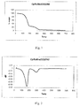
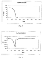
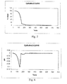
- substitution of the Cp ring and tailoring of the alkyl group bonded to the metal has shown useful properties for chemical phase deposition processes such as CVD or ALD, or a hybrid of CVD and ALD. Examples of such useful properties include higher vapor pressure (as demonstrated in Figure 14 ) and greater thermal stability (as demonstrated in Figures 1-9 ). Further, is has been discovered that addition of the alkyl groups provides better adhesion to the substrate, and carbon free layers under ALD conditions. Though substituted-Cp precursors have shown useful properties, it is possible to use both the substituted and unsubstituted Cp precursors of the present invention in chemical phase deposition processes.
- a method of forming a metal-containing thin film by ALD comprises delivering at least one precursor to a substrate, wherein the precursor corresponds in structure to Formula II: Cp(R) n M(CO) 2 (X) (Formula II) wherein:
- a method of forming a metal-containing thin film by CVD comprises delivering at least one precursor to a substrate, wherein the precursor corresponds in structure to Formula II above.
- the precursor corresponds in structure to Formula II wherein:
- the precursor corresponds in structure to Formula II wherein:
- the precursor corresponds in structure to Formula II wherein:
- the precursor corresponds in structure to Formula II wherein:
- the precursor according to Formula II is selected from the group consisting of:
- the precursor according to Formula II is selected from the group consisting of:
- the precursor corresponding in structure to Formula II is (cyclopentadienyl)ruthenium(ethyl)(dicarbonyl).
- the precursor corresponds in structure to Formula I and/or II, wherein butyl is selected from the group consisting of n -butyl, sec- butyl, iso -butyl and tert -butyl.
- the precursor corresponds in structure to Formula I and/or II, wherein propyl is selected from the group consisting of n -propyl and iso -propyl.
- the chemical phase deposition processes described herein can be used to form various metal-containing thin films, such as metal or metal oxide films, on substrates using at least one of the organometallic precursors according to Formula II.
- the film can be formed by the organometallic precursor independently or in combination with a co-reactant (can be referred to as co-precursor).
- co-reactants include, but are not limited to hydrogen, hydrogen plasma, oxygen, air, water, ammonia, hydrazine, allylhydrazine, borane, silane, ozone or any combination thereof.
- the at least one precursor is delivered to the substrate in pulses alternating with pulses of an oxygen source to create a metal oxide film.
- oxygen sources include, without limitation, H 2 O, O 2 or ozone.
- substrates can be used in the methods described herein.
- the precursors according to Formula I and/or II may be delivered for deposition on substrates such as, but not limited to, silicon, silicon oxide, silicon nitride, tantalum, tantalum nitride, or copper.
- the ALD and CVD methods described herein encompass various types of ALD and CVD processes such as, but not limited to, conventional processes, liquid injection processes and photo-assisted processes.
- conventional CVD is used to form a metal-containing thin film using at least one precursor according to Formula I and/or II.
- CVD processes see for example Smith, Donald (1995). Thin-Film Deposition: Principles and Practice. McGraw-Hill .
- liquid injection CVD is used to form a metal-containing thin film using at least one precursor according to Formula I and/or II.
- liquid injection CVD growth conditions include, but are not limited to:
- photo-assisted CVD is used to form a metal-containing thin film using at least one precursor according to Formula I and/or II.
- conventional ALD is used to form a metal-containing thin film using at least one precursor according to Formula I and/or II.
- ALD pulsed injection ALD process
- liquid injection ALD is used form a metal-containing thin film using at least one precursor according to Formula I and/or II, wherein at least one liquid precursor is delivered to the reaction chamber by direct liquid injection as opposed to vapor draw by a bubbler.
- liquid injection ALD process see, for example, Potter R. J., et. al. Chem. Vap. Deposition. 2005. 11(3):159 .
- liquid injection ALD growth conditions include, but are not limited to:
- photo-assisted ALD is used to form a metal-containing thin film using at least one precursor according to Formula I and/or II.
- photo-assisted ALD processes see, for example, U.S. Patent No. 4,581,249 .
- organometallic precursors, according to Formula I or II, utilized in these methods may be liquid, solid, or gaseous.
- Ruthenium precursors of Formula I and/or II can be made by the following method:
- ruthenium precursors of Formula I and/or II can be made by the following method:
- the precursors and methods disclosed herein are useful in semiconductor devices and are useful for computer memory and logic applications, such as dynamic random access memory (DRAM) and complementary metal oxide semi-conductor (CMOS) circuitry. They are useful in many applications such as capacitor electrodes, gate electrodes and as adhesive diffusion barrier metal.
- DRAM dynamic random access memory
- CMOS complementary metal oxide semi-conductor
- Precursors contemplated by the invention include, but are not limited to those listed below. It will be noted that when n is zero, there is no R substituent and the cyclopentadienyl ligand is therefore unsubstituted. Further, the R substituent is ⁇ -bonded and its depiction below represents that the cyclopentadienyl ligand may be substituted zero to five times. Precursor No.
- Ru 3 (CO) 12 (15.0g, 23.5 mmols) was reacted with CpMeH in the normal manner except that solution was heated for 1.5 hours instead of 1.0 hour and reaction with oxygenated heptane for 2.5 hours rather than 2.0 hours. After cooling overnight, orange crystalline material (12.1g, 73%) was obtained. The solution is reduced to 100 ml and a further (1.9g, 11%) darker, crystalline material was obtained after standing overnight. Total yield 84%. IR (hexane) 2007m, 1968m, 1960s, 1940m, 1788s cm -1 ; (CH 2 Cl 2 ) 1997s, 1953s, 1767s cm -1 .
- Solvent was removed on rotavap ( ⁇ 70 mm Hg) to give an oil which was dissolved in hexane ( ⁇ 150 ml). Following filtration, solvent was removed on the rotavap, the oil was transferred to a small flask and the residual hexane was removed at 0.5 mm Hg to give 22g of a dark red oil. Distillation was performed twice at 58-60°C (0.5mm Hg) to give a pale yellow mobile oil (17.1g, 79) of ( ⁇ 5 -CpMe)Ru(Me)(CO) 2 depicted below.
- CpRu(Et)(CO) 2 also referred to herein as (cyclopentadienyl)ruthenium(ethyl)(dicarbonyl) and depicted below] is demonstrated below.
- CpRu(Et)(CO) 2 A further synthesis scheme and a method to prepare CpRu(Et)(CO) 2 is demonstrated below.
- CpRuMe(CO) 2 also referred to herein as (cyclopentadienyl)ruthenium(methyl)(dicarbonyl)
- Ruthenium thin films were deposited in a custom-built ALD reactor. Cyclopentadienyl ruthenium (methyl)dicarbonyl (CpRuMe(CO) 2 ) and air were used as precursors. The ruthenium films were deposited on silicon wafer substrates. Prior to deposition, the wafer substrates were dipped in a 10% HF:water mixture for 30 seconds. The growth temperature was 300°C. The growth pressure is 250 millitorr. The reactor is continuously purged with 30 sccm of dry nitrogen. All the computer controlled valves in the reactor were the air operated ALD VCR valves from Cajon.
- the amount of injected air was the volume trapped between the VCR gasket (a blank gasket with a 30 micron pin hole in it) and the ALD valve stem. For air at atmospheric pressure and temperature, this means that approximately 29 ⁇ moles of air is pulsed into the reactor during the air injection cycle.
- the pulse length of the air precursor is approximately 1 second followed by a 2-5 second purge. No ruthenium was deposited when the air inject line was plugged.
- the ruthenium was stored in a stainless steel ampoule. Attached directly to the ampoule was an air operated ALD valve. The output of this ALD valve was Tee'd with another ALD valve used for nitrogen injection. The Tee outlet leg was connected to a 500 cm 3 stainless steel reservoir. The outlet of the reservoir was attached to a third ALD valve, called the inject valve, whose outlet goes directly to the reactor. Nitrogen injection was used to build up the total pressure behind the ruthenium inject valve so that the pressure was higher than the reactor growth pressure. The injected nitrogen was accomplished using a 30 micron pin hole VCR gasket as described above for air injection. All of the valves and ampoule were placed into an oven-like enclosure that allowed the ampoule, valves, and tubing to be heated uniformly to 50°C to 120°C.
- the valves were sequenced in the following manner. Immediately after an air injection, the ruthenium ampoule ALD valve and the nitrogen inject ALD valve were both opened. The nitrogen inject valve was closed after 0.2 seconds. The ruthenium vapors and injected nitrogen were allowed to equilibrate in the 500 cm 3 reservoir during the air purge time (typically 2-5 seconds). After the air purge time had elapsed, the ruthenium ampoule ALD valve was closed, and after a 0.2 second wait time, the ruthenium inject valve was opened for 0.2 seconds. The ruthenium was allowed to purge from the reactor for typically 5 seconds. The air was then injected to start the ALD cycle all over again.
- the effect of the dose of ruthenium precursor was investigated by varying the precursor temperature from 85°C to 110°C.
- the growth at 85°C is non-uniform.
- the growth with precursor temperature between 90°C to 110°C is uniform. Normal growth temperature is usually 90°C.
- the films produce a featureless scanning electron micrograph as shown in Figure 15 .
- the resistivity of the films is 22-25 micro ohm cm.
- AFM spectroscopy at various cycles (50-300 cycles) shows the growth process via island formation. See Figure 10 .
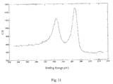
- XPS of the ALD grown ruthenium films demonstrate the absence of carbon in the films. See Figures 11 and 12 .
- ALD growth using CpRuMe(CO) 2 was also performed as in Example 4, except using an argon purge, as opposed to nitrogen, a ruthenium pulse length of 1 second, an air pulse length of 1 second.
- CpRuEt(CO) 2 also referred to herein as (cyclopentadienyl)ruthenium(ethyl)(dicarbonyl)] and depicted below is demonstrated by the following example.
- Ruthenium thin films were deposited in a custom-built ALD reactor. Cyclopentadienyl ruthenium (ethyl)dicarbonyl (CpRuEt(CO) 2 ) and air was used as precursors. The ruthenium films were deposited on silicon wafer substrates. Prior to deposition, the wafer substrates were dipped in a 10% HF:water mixture for 30 seconds. The growth temperature was 265°C. The growth pressure was 100 milliTorr. The reactor was continuously purged with 10 sccm of argon. All the computer controlled valves in the reactor are the air operated ALD VCR valves from Cajon.
- the amount of injected air was the volume trapped between the VCR gasket (a blank gasket with a 30 micron pin hole in it) and the ALD valve stem. For air at atmospheric pressure and temperature, this means that approximately 29 ⁇ moles of air is pulsed into the reactor during the air injection cycle.
- the pulse length of the air precursor is approximately 2 seconds followed by a 2-5 second purge. No ruthenium was deposited when the air inject line was plugged.
- the ruthenium was stored in a stainless steel ampoule. Attached directly to the ampoule was an air operated ALD valve. The output of this ALD valve was Tee'd with another ALD valve used for argon injection. The Tee outlet leg was connected to a 500 cm 3 stainless steel reservoir. The outlet of the reservoir was attached to a third ALD valve, called the inject valve, whose outlet goes directly to the reactor. Argon injection was used to build up the total pressure behind the ruthenium inject valve so that the pressure is higher than the reactor growth pressure. The injected argon was accomplished using a 30 micron pin hole VCR gasket as described above for air injection. All of the valves and ampoule were placed into an oven-like enclosure that allowed the ampoule, valves, and tubing to be heated uniformly to 50°C to 120°C.
- the valves were sequenced in the following manner. Immediately after an air injection, the ruthenium ampoule ALD valve and the argon inject ALD valve were both opened. The argon inject valve was closed after 0.2 seconds. The ruthenium vapors and injected argon were allowed to equilibrate in the 500 cm 3 reservoir during the air purge time (typically 2-5 seconds). After the air purge time had elapsed, the ruthenium ampoule ALD valve was closed, and after a 0.2 second wait time, the ruthenium inject valve was opened for 2 seconds. The ruthenium was allowed to purge from the reactor for typically 5 seconds. The air was then injected to start the ALD cycle all over again.
- the effect of the dose of ruthenium precursor was investigated by varying the precursor temperature from 85°C to 110°C.
- the growth at 85°C is non-uniform.
- the growth with precursor temperature between 90°C to 110°C is uniform. Normal growth temperature is usually 90°C.
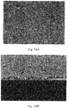
- Figures 16A, 16B and 16C display three scanning electron micrographs of ruthenium films grown using CpRuEt(CO) 2 . Continuous films with resistances less than 100 mega ohm/square were grown with RMS surface roughness of 2.1 nm.
- Example 6 was repeated using the various substrates and cycles listed in the table below. Good growth was seen on metal substrates throughout an 800 cycle run. Substrate/cycles 200 400 600 800 Si (H-terminated) No growth Good growth, poor coverage Growth, rough surface Growth, very rough surface SiO 2 (native oxide) Some growth, poor coverage Good growth good coverage Growth, rough surface Growth, very rough surface Ta/Cu Metal Good growth Good growth Good growth Good growth Good growth Good growth Good growth Good growth
- Figure 17 is a graphical representation of ALD growth rate of ruthenium films on Ta substrate using CpRuEt(CO) 2 . A growth rate of 0.95 Angstroms/cycle was achieved. Growth was measured by XRF and calibrated with a thick sample measured by SEM.
Landscapes
- Chemical & Material Sciences (AREA)
- Organic Chemistry (AREA)
- General Chemical & Material Sciences (AREA)
- Chemical Kinetics & Catalysis (AREA)
- Engineering & Computer Science (AREA)
- Materials Engineering (AREA)
- Mechanical Engineering (AREA)
- Metallurgy (AREA)
- Chemical Vapour Deposition (AREA)
- Electrodes Of Semiconductors (AREA)
- Organic Low-Molecular-Weight Compounds And Preparation Thereof (AREA)
Claims (9)
- Metallorganischer Komplex, dargestellt durch die Formel I:
Cp(R)nM(CO)2(X) (Formel I)
worinM Ru oder Os ist;R C1-C10-Alkyl ist;X C1-C10-Alkyl ist; undn 1, 2, 3 oder 4 ist. - Metallorganischer Komplex gemäß Anspruch 1, worin
M Ru ist;
R ausgewählt ist aus der Gruppe Methyl, Ethyl, Propyl und Butyl;
X ausgewählt ist aus der Gruppe Methyl, Ethyl, Propyl und Butyl; und
n 1, 2, 3 oder 4 ist. - Metallorganischer Komplex gemäß Anspruch 1, worin
M Os ist;
R ausgewählt ist aus der Gruppe Methyl, Ethyl Propyl und Butyl;
X ausgewählt ist aus der Gruppe Methyl, Ethyl, Propyl und Butyl; und
n 1, 2, 3 oder 4 ist. - Metallorganischer Komplex gemäß Anspruch 1, worin
X ausgewählt ist aus der Gruppe Methyl, Ethyl und Propyl;
R ausgewählt ist aus der Gruppe Methyl, Ethyl und Propyl; und
n 2, 3 oder 4 ist. - Metallorganischer Komplex gemäß Anspruch 1, worin
M Ru ist;
X Methyl oder Ethyl ist;
R Methyl oder Ethyl ist; und
n 1 ist. - Metallorganischer Komplex gemäß Anspruch 1, worin
M Os ist;
X Methyl oder Ethyl ist;
R Methyl oder Ethyl ist; und
n 1 ist. - Metallorganischer Komplex gemäß Anspruch 1, worin Butyl ausgewählt ist aus der Gruppe n-Butyl, sec-Butyl, iso-Butyl und tert-Butyl.
- Metallorganischer Komplex gemäß Anspruch 1, worin Propyl ausgewählt ist aus der Gruppe n-Propyl und iso-Propyl.
- Metallorganischer Komplex gemäß Anspruch 1, worin der Komplex ausgewählt ist aus der Gruppe(Methylcyclopentadienyl)ruthenium(methyl)(dicarbonyl);(Ethylcyclopentadienyl)ruthenium(methyl)(dicarbonyl);(Propylcyclopentadienyl)ruthenium(methyl)(dicarbonyl);(Butylcyclopentadienyl)ruthenium(methyl)(dicarbonyl);(Methylcyclopentadienyl)ruthenium(ethyl)(dicarbonyl);(Ethylcyclopentadienyl)ruthenium(ethyl)(dicarbonyl);(Propylcyclopentadienyl)ruthenium(ethyl)(dicarbonyl);(Butylcyclopentadienyl)ruthenium(ethyl)(dicarbonyl);(Methylcyclopentadienyl)osmium(methyl)(dicarbonyl);(Ethylcyclopentadienyl)osmium(methyl)(dicarbonyl);(Propylcyclopentadienyl)osmium(methyl)(dicarbonyl);(Butylcyclopentadienyl)osmium(methyl)(dicarbonyl);(Methylcyclopentadienyl)osmium(ethyl)(dicarbonyl);(Ethylcyclopentadienyl)osmium(ethyl)(dicarbonyl);(Propylcyclopentadienyl)osmium(ethyl)(dicarbonyl); und(Butylcyclopentadienyl)osmium(ethyl)(dicarbonyl).
Applications Claiming Priority (2)
| Application Number | Priority Date | Filing Date | Title |
|---|---|---|---|
| US95160107P | 2007-07-24 | 2007-07-24 | |
| PCT/US2008/071014 WO2009015270A1 (en) | 2007-07-24 | 2008-07-24 | Organometallic precursors for use in chemical phase deposition processes |
Publications (2)
| Publication Number | Publication Date |
|---|---|
| EP2178894A1 EP2178894A1 (de) | 2010-04-28 |
| EP2178894B1 true EP2178894B1 (de) | 2016-10-19 |
Family
ID=39828988
Family Applications (1)
| Application Number | Title | Priority Date | Filing Date |
|---|---|---|---|
| EP08782322.5A Not-in-force EP2178894B1 (de) | 2007-07-24 | 2008-07-24 | Metallorganische vorstufen zur verwendung bei abscheidungsverfahren in der chemischen phase |
Country Status (7)
| Country | Link |
|---|---|
| US (1) | US8476467B2 (de) |
| EP (1) | EP2178894B1 (de) |
| JP (1) | JP5528338B2 (de) |
| KR (1) | KR101577676B1 (de) |
| CN (1) | CN101801988B (de) |
| TW (1) | TWI382987B (de) |
| WO (1) | WO2009015270A1 (de) |
Families Citing this family (13)
| Publication number | Priority date | Publication date | Assignee | Title |
|---|---|---|---|---|
| GB2432363B (en) * | 2005-11-16 | 2010-06-23 | Epichem Ltd | Hafnocene and zirconocene precursors, and use thereof in atomic layer deposition |
| TWI425110B (zh) | 2007-07-24 | 2014-02-01 | 辛格瑪艾瑞契公司 | 以化學相沉積法製造含金屬薄膜之方法 |
| TWI382987B (zh) | 2007-07-24 | 2013-01-21 | Sigma Aldrich Co | 應用於化學相沉積製程的有機金屬前驅物 |
| KR101560755B1 (ko) | 2007-09-14 | 2015-10-15 | 시그마 알드리치 컴퍼니 엘엘씨 | 모노시클로펜타디에닐 티타늄계 전구체를 이용한 원자층 증착에 의한 티타늄 함유 박막의 제조 방법 |
| US20090205538A1 (en) * | 2008-01-24 | 2009-08-20 | Thompson David M | Organometallic compounds, processes for the preparation thereof and methods of use thereof |
| TWI467045B (zh) * | 2008-05-23 | 2015-01-01 | Sigma Aldrich Co | 高介電常數電介質薄膜與使用鈰基前驅物製造高介電常數電介質薄膜之方法 |
| TW200949939A (en) * | 2008-05-23 | 2009-12-01 | Sigma Aldrich Co | High-k dielectric films and methods of producing using titanium-based β -diketonate precursors |
| CN102574884B (zh) | 2009-08-07 | 2016-02-10 | 西格玛-奥吉奇有限责任公司 | 高分子量烷基-烯丙基三羰基钴配合物及其用于制备介电薄膜的用途 |
| SG187920A1 (en) | 2010-08-27 | 2013-03-28 | Sigma Aldrich Co Llc | Molybdenum (iv) amide precursors and use thereof in atomic layer deposition |
| US8927748B2 (en) | 2011-08-12 | 2015-01-06 | Sigma-Aldrich Co. Llc | Alkyl-substituted allyl carbonyl metal complexes and use thereof for preparing dielectric thin films |
| WO2013112383A1 (en) | 2012-01-26 | 2013-08-01 | Sigma-Aldrich Co. Llc | Molybdenum allyl complexes and use thereof in thin film deposition |
| CN111655899A (zh) | 2018-02-12 | 2020-09-11 | 默克专利有限公司 | 使用无氧共反应物气相沉积钌的方法 |
| EP4702031A1 (de) | 2023-04-25 | 2026-03-04 | Heraeus Precious Metals GmbH & Co. KG | Neue halbsandwichkomplexe des rutheniums |
Family Cites Families (39)
| Publication number | Priority date | Publication date | Assignee | Title |
|---|---|---|---|---|
| US3253946A (en) | 1960-08-11 | 1966-05-31 | Ethyl Corp | Vapor plating with manganese, chromium, molybdenum or tungsten employing cyclopentadienyl metal carbonyl |
| JPH07107190B2 (ja) | 1984-03-30 | 1995-11-15 | キヤノン株式会社 | 光化学気相成長方法 |
| GB9929279D0 (en) | 1999-12-11 | 2000-02-02 | Epichem Ltd | An improved method of and apparatus for the delivery of precursors in the vapour phase to a plurality of epitaxial reactor sites |
| GB0017968D0 (en) | 2000-07-22 | 2000-09-13 | Epichem Ltd | An improved process and apparatus for the isolation of pure,or substantially pure,organometallic compounds |
| JP3830785B2 (ja) * | 2001-08-10 | 2006-10-11 | 田中貴金属工業株式会社 | Cvd用の有機ルテニウム化合物の製造方法及びcvd用の有機ルテニウム化合物 |
| US6420583B1 (en) | 2001-09-27 | 2002-07-16 | Praxair Technology, Inc | Methods of synthesizing ruthenium and osmium compounds |
| ATE340800T1 (de) | 2001-10-26 | 2006-10-15 | Epichem Ltd | Vorlaeuferverbindungen für chemische dampfphasenabscheidung |
| DE602004014258D1 (de) | 2003-03-17 | 2008-07-17 | Sigma Aldrich Co | Alkoholate der seltenerdmetalle als vorstufen für metalloxidschichten und -filme |
| JP4154729B2 (ja) | 2003-11-12 | 2008-09-24 | Jsr株式会社 | 導電性積層膜およびその導電性積層膜形成方法 |
| JP4386177B2 (ja) | 2004-01-26 | 2009-12-16 | Jsr株式会社 | 導電性積層膜およびその形成方法 |
| US7244858B2 (en) | 2004-03-25 | 2007-07-17 | Praxair Technology, Inc. | Organometallic precursor compounds |
| GB0412790D0 (en) | 2004-06-08 | 2004-07-14 | Epichem Ltd | Precursors for deposition of silicon nitride,silicon oxynitride and metal silicon oxynitrides |
| WO2006023501A2 (en) | 2004-08-16 | 2006-03-02 | Aviza Technology, Inc. | Direct liquid injection system and method for forming multi-component dielectric films |
| US7476618B2 (en) | 2004-10-26 | 2009-01-13 | Asm Japan K.K. | Selective formation of metal layers in an integrated circuit |
| JP5053543B2 (ja) | 2005-02-02 | 2012-10-17 | 東ソー株式会社 | タンタル化合物、その製造方法、タンタル含有薄膜、及びその形成方法 |
| GB2432363B (en) | 2005-11-16 | 2010-06-23 | Epichem Ltd | Hafnocene and zirconocene precursors, and use thereof in atomic layer deposition |
| GB2432371B (en) | 2005-11-17 | 2011-06-15 | Epichem Ltd | Improved bubbler for the transportation of substances by a carrier gas |
| US8153831B2 (en) | 2006-09-28 | 2012-04-10 | Praxair Technology, Inc. | Organometallic compounds, processes for the preparation thereof and methods of use thereof |
| US20080248648A1 (en) | 2007-04-06 | 2008-10-09 | Thompson David M | Deposition precursors for semiconductor applications |
| TWI425110B (zh) | 2007-07-24 | 2014-02-01 | 辛格瑪艾瑞契公司 | 以化學相沉積法製造含金屬薄膜之方法 |
| TWI382987B (zh) | 2007-07-24 | 2013-01-21 | Sigma Aldrich Co | 應用於化學相沉積製程的有機金屬前驅物 |
| KR101560755B1 (ko) | 2007-09-14 | 2015-10-15 | 시그마 알드리치 컴퍼니 엘엘씨 | 모노시클로펜타디에닐 티타늄계 전구체를 이용한 원자층 증착에 의한 티타늄 함유 박막의 제조 방법 |
| KR20100072021A (ko) | 2007-09-14 | 2010-06-29 | 시그마-알드리치컴퍼니 | 하프늄과 지르코늄계 전구체를 이용한 원자층 증착에 의한 박막의 제조 방법 |
| WO2009086263A1 (en) | 2007-12-28 | 2009-07-09 | Sigma-Aldrich Co. | Methods for preparing thin films using substituted pyrrolyl-metal precursors |
| TW200944535A (en) | 2008-03-20 | 2009-11-01 | Sigma Aldrich Co | Purification and preparation of phosphorus-containing compounds |
| TWI467045B (zh) | 2008-05-23 | 2015-01-01 | Sigma Aldrich Co | 高介電常數電介質薄膜與使用鈰基前驅物製造高介電常數電介質薄膜之方法 |
| TW200949006A (en) | 2008-05-23 | 2009-12-01 | Sigma Aldrich Co | High-k dielectric films and methods of producing using titanium-based precursors |
| TW200949939A (en) | 2008-05-23 | 2009-12-01 | Sigma Aldrich Co | High-k dielectric films and methods of producing using titanium-based β -diketonate precursors |
| WO2009143452A1 (en) | 2008-05-23 | 2009-11-26 | Sigma-Aldrich Co. | High-k dielectric films and methods of producing using cerium-based precursors |
| TW200951241A (en) | 2008-05-30 | 2009-12-16 | Sigma Aldrich Co | Methods of forming ruthenium-containing films by atomic layer deposition |
| TW201014924A (en) | 2008-06-20 | 2010-04-16 | Sigma Aldrich Co | Hafnium and zirconium pyrrolyl-based organometallic precursors and use thereof for preparing dielectric thin films |
| WO2010021891A1 (en) | 2008-08-18 | 2010-02-25 | Sigma-Aldrich Co. | Valve assemblies |
| WO2011011299A1 (en) | 2009-07-21 | 2011-01-27 | Sigma-Aldrich Co. | Compositions and methods of use for forming titanium- containing thin films |
| CN102574884B (zh) | 2009-08-07 | 2016-02-10 | 西格玛-奥吉奇有限责任公司 | 高分子量烷基-烯丙基三羰基钴配合物及其用于制备介电薄膜的用途 |
| EP2496733B1 (de) | 2009-11-02 | 2021-08-04 | Sigma-Aldrich Co. LLC | Methode zum verdampfen |
| WO2011097100A1 (en) | 2010-02-02 | 2011-08-11 | Sigma-Aldrich Co. | Vapor product delivery assemblies and related methods |
| WO2011112413A1 (en) | 2010-03-10 | 2011-09-15 | Sigma-Aldrich Co. | Delivery assemblies and related methods |
| US20130052368A1 (en) | 2010-03-19 | 2013-02-28 | Sigma-Aldrich Co. Llc | Methods for preparing thin films by atomic layer deposition using hydrazines |
| SG187920A1 (en) | 2010-08-27 | 2013-03-28 | Sigma Aldrich Co Llc | Molybdenum (iv) amide precursors and use thereof in atomic layer deposition |
-
2008
- 2008-07-23 TW TW097127957A patent/TWI382987B/zh active
- 2008-07-24 EP EP08782322.5A patent/EP2178894B1/de not_active Not-in-force
- 2008-07-24 CN CN200880106411.1A patent/CN101801988B/zh active Active
- 2008-07-24 US US12/670,022 patent/US8476467B2/en active Active
- 2008-07-24 WO PCT/US2008/071014 patent/WO2009015270A1/en not_active Ceased
- 2008-07-24 JP JP2010518382A patent/JP5528338B2/ja active Active
- 2008-07-24 KR KR1020107003167A patent/KR101577676B1/ko active Active
Non-Patent Citations (1)
| Title |
|---|
| None * |
Also Published As
| Publication number | Publication date |
|---|---|
| JP2010534678A (ja) | 2010-11-11 |
| WO2009015270A4 (en) | 2009-04-02 |
| US20100256406A1 (en) | 2010-10-07 |
| CN101801988A (zh) | 2010-08-11 |
| KR20100046193A (ko) | 2010-05-06 |
| KR101577676B1 (ko) | 2015-12-15 |
| WO2009015270A1 (en) | 2009-01-29 |
| JP5528338B2 (ja) | 2014-06-25 |
| US8476467B2 (en) | 2013-07-02 |
| EP2178894A1 (de) | 2010-04-28 |
| CN101801988B (zh) | 2013-03-06 |
| TW200918543A (en) | 2009-05-01 |
| TWI382987B (zh) | 2013-01-21 |
Similar Documents
| Publication | Publication Date | Title |
|---|---|---|
| US8481121B2 (en) | Methods of forming thin metal-containing films by chemical phase deposition | |
| US8476467B2 (en) | Organometallic precursors for use in chemical phase deposition processes | |
| US10914001B2 (en) | Volatile dihydropyrazinly and dihydropyrazine metal complexes | |
| EP2191034B1 (de) | Verfahren zur herstellung von dünnen filmen durch atomlagenabscheidung unter verwendung von monocyclopentadnieyltriaminozirconium-vorläufern | |
| EP2609102B1 (de) | Molybdän (iv)-amidvorläufer und ihre verwendung in der atomlagenabscheidung | |
| TWI397532B (zh) | Method for producing film and film for film formation | |
| JP7773735B2 (ja) | 金属含有膜の生成方法 | |
| CN101516900A (zh) | 有机金属前体化合物 | |
| WO2009094262A1 (en) | Organometallic compounds, processes and methods of use | |
| WO2009094263A1 (en) | Organometallic compounds, processes and methods of use | |
| KR102815650B1 (ko) | 4족 전이금속 함유 박막 형성용 전구체 및 이를 이용한 4족 전이금속 함유 박막 형성 방법. |
Legal Events
| Date | Code | Title | Description |
|---|---|---|---|
| PUAI | Public reference made under article 153(3) epc to a published international application that has entered the european phase |
Free format text: ORIGINAL CODE: 0009012 |
|
| 17P | Request for examination filed |
Effective date: 20100217 |
|
| AK | Designated contracting states |
Kind code of ref document: A1 Designated state(s): AT BE BG CH CY CZ DE DK EE ES FI FR GB GR HR HU IE IS IT LI LT LU LV MC MT NL NO PL PT RO SE SI SK TR |
|
| AX | Request for extension of the european patent |
Extension state: AL BA MK RS |
|
| DAX | Request for extension of the european patent (deleted) | ||
| 17Q | First examination report despatched |
Effective date: 20121008 |
|
| RAP1 | Party data changed (applicant data changed or rights of an application transferred) |
Owner name: SIGMA-ALDRICH CO. LLC |
|
| GRAP | Despatch of communication of intention to grant a patent |
Free format text: ORIGINAL CODE: EPIDOSNIGR1 |
|
| RIC1 | Information provided on ipc code assigned before grant |
Ipc: C07F 15/02 20060101ALI20160307BHEP Ipc: C23C 16/16 20060101ALI20160307BHEP Ipc: C07F 15/00 20060101AFI20160307BHEP Ipc: C23C 16/455 20060101ALI20160307BHEP Ipc: C23C 16/18 20060101ALI20160307BHEP Ipc: C07F 17/02 20060101ALI20160307BHEP |
|
| INTG | Intention to grant announced |
Effective date: 20160404 |
|
| GRAS | Grant fee paid |
Free format text: ORIGINAL CODE: EPIDOSNIGR3 |
|
| GRAJ | Information related to disapproval of communication of intention to grant by the applicant or resumption of examination proceedings by the epo deleted |
Free format text: ORIGINAL CODE: EPIDOSDIGR1 |
|
| GRAL | Information related to payment of fee for publishing/printing deleted |
Free format text: ORIGINAL CODE: EPIDOSDIGR3 |
|
| GRAR | Information related to intention to grant a patent recorded |
Free format text: ORIGINAL CODE: EPIDOSNIGR71 |
|
| GRAA | (expected) grant |
Free format text: ORIGINAL CODE: 0009210 |
|
| RIN1 | Information on inventor provided before grant (corrected) |
Inventor name: ODEDRA, RAJ Inventor name: BOAG, NEIL Inventor name: KANJOLIA, RAVI |
|
| INTC | Intention to grant announced (deleted) | ||
| AK | Designated contracting states |
Kind code of ref document: B1 Designated state(s): AT BE BG CH CY CZ DE DK EE ES FI FR GB GR HR HU IE IS IT LI LT LU LV MC MT NL NO PL PT RO SE SI SK TR |
|
| INTG | Intention to grant announced |
Effective date: 20160912 |
|
| REG | Reference to a national code |
Ref country code: GB Ref legal event code: FG4D |
|
| REG | Reference to a national code |
Ref country code: CH Ref legal event code: EP |
|
| REG | Reference to a national code |
Ref country code: AT Ref legal event code: REF Ref document number: 838233 Country of ref document: AT Kind code of ref document: T Effective date: 20161115 |
|
| REG | Reference to a national code |
Ref country code: IE Ref legal event code: FG4D |
|
| REG | Reference to a national code |
Ref country code: DE Ref legal event code: R096 Ref document number: 602008046936 Country of ref document: DE |
|
| REG | Reference to a national code |
Ref country code: NL Ref legal event code: MP Effective date: 20161019 |
|
| REG | Reference to a national code |
Ref country code: LT Ref legal event code: MG4D |
|
| PG25 | Lapsed in a contracting state [announced via postgrant information from national office to epo] |
Ref country code: LV Free format text: LAPSE BECAUSE OF FAILURE TO SUBMIT A TRANSLATION OF THE DESCRIPTION OR TO PAY THE FEE WITHIN THE PRESCRIBED TIME-LIMIT Effective date: 20161019 |
|
| REG | Reference to a national code |
Ref country code: AT Ref legal event code: MK05 Ref document number: 838233 Country of ref document: AT Kind code of ref document: T Effective date: 20161019 |
|
| PG25 | Lapsed in a contracting state [announced via postgrant information from national office to epo] |
Ref country code: NO Free format text: LAPSE BECAUSE OF FAILURE TO SUBMIT A TRANSLATION OF THE DESCRIPTION OR TO PAY THE FEE WITHIN THE PRESCRIBED TIME-LIMIT Effective date: 20170119 Ref country code: LT Free format text: LAPSE BECAUSE OF FAILURE TO SUBMIT A TRANSLATION OF THE DESCRIPTION OR TO PAY THE FEE WITHIN THE PRESCRIBED TIME-LIMIT Effective date: 20161019 Ref country code: SE Free format text: LAPSE BECAUSE OF FAILURE TO SUBMIT A TRANSLATION OF THE DESCRIPTION OR TO PAY THE FEE WITHIN THE PRESCRIBED TIME-LIMIT Effective date: 20161019 Ref country code: GR Free format text: LAPSE BECAUSE OF FAILURE TO SUBMIT A TRANSLATION OF THE DESCRIPTION OR TO PAY THE FEE WITHIN THE PRESCRIBED TIME-LIMIT Effective date: 20170120 |
|
| PG25 | Lapsed in a contracting state [announced via postgrant information from national office to epo] |
Ref country code: HR Free format text: LAPSE BECAUSE OF FAILURE TO SUBMIT A TRANSLATION OF THE DESCRIPTION OR TO PAY THE FEE WITHIN THE PRESCRIBED TIME-LIMIT Effective date: 20161019 Ref country code: FI Free format text: LAPSE BECAUSE OF FAILURE TO SUBMIT A TRANSLATION OF THE DESCRIPTION OR TO PAY THE FEE WITHIN THE PRESCRIBED TIME-LIMIT Effective date: 20161019 Ref country code: PT Free format text: LAPSE BECAUSE OF FAILURE TO SUBMIT A TRANSLATION OF THE DESCRIPTION OR TO PAY THE FEE WITHIN THE PRESCRIBED TIME-LIMIT Effective date: 20170220 Ref country code: NL Free format text: LAPSE BECAUSE OF FAILURE TO SUBMIT A TRANSLATION OF THE DESCRIPTION OR TO PAY THE FEE WITHIN THE PRESCRIBED TIME-LIMIT Effective date: 20161019 Ref country code: ES Free format text: LAPSE BECAUSE OF FAILURE TO SUBMIT A TRANSLATION OF THE DESCRIPTION OR TO PAY THE FEE WITHIN THE PRESCRIBED TIME-LIMIT Effective date: 20161019 Ref country code: IS Free format text: LAPSE BECAUSE OF FAILURE TO SUBMIT A TRANSLATION OF THE DESCRIPTION OR TO PAY THE FEE WITHIN THE PRESCRIBED TIME-LIMIT Effective date: 20170219 Ref country code: AT Free format text: LAPSE BECAUSE OF FAILURE TO SUBMIT A TRANSLATION OF THE DESCRIPTION OR TO PAY THE FEE WITHIN THE PRESCRIBED TIME-LIMIT Effective date: 20161019 Ref country code: PL Free format text: LAPSE BECAUSE OF FAILURE TO SUBMIT A TRANSLATION OF THE DESCRIPTION OR TO PAY THE FEE WITHIN THE PRESCRIBED TIME-LIMIT Effective date: 20161019 |
|
| REG | Reference to a national code |
Ref country code: FR Ref legal event code: PLFP Year of fee payment: 10 |
|
| REG | Reference to a national code |
Ref country code: DE Ref legal event code: R097 Ref document number: 602008046936 Country of ref document: DE |
|
| PG25 | Lapsed in a contracting state [announced via postgrant information from national office to epo] |
Ref country code: EE Free format text: LAPSE BECAUSE OF FAILURE TO SUBMIT A TRANSLATION OF THE DESCRIPTION OR TO PAY THE FEE WITHIN THE PRESCRIBED TIME-LIMIT Effective date: 20161019 Ref country code: DK Free format text: LAPSE BECAUSE OF FAILURE TO SUBMIT A TRANSLATION OF THE DESCRIPTION OR TO PAY THE FEE WITHIN THE PRESCRIBED TIME-LIMIT Effective date: 20161019 Ref country code: SK Free format text: LAPSE BECAUSE OF FAILURE TO SUBMIT A TRANSLATION OF THE DESCRIPTION OR TO PAY THE FEE WITHIN THE PRESCRIBED TIME-LIMIT Effective date: 20161019 Ref country code: CZ Free format text: LAPSE BECAUSE OF FAILURE TO SUBMIT A TRANSLATION OF THE DESCRIPTION OR TO PAY THE FEE WITHIN THE PRESCRIBED TIME-LIMIT Effective date: 20161019 Ref country code: RO Free format text: LAPSE BECAUSE OF FAILURE TO SUBMIT A TRANSLATION OF THE DESCRIPTION OR TO PAY THE FEE WITHIN THE PRESCRIBED TIME-LIMIT Effective date: 20161019 |
|
| PLBE | No opposition filed within time limit |
Free format text: ORIGINAL CODE: 0009261 |
|
| STAA | Information on the status of an ep patent application or granted ep patent |
Free format text: STATUS: NO OPPOSITION FILED WITHIN TIME LIMIT |
|
| PG25 | Lapsed in a contracting state [announced via postgrant information from national office to epo] |
Ref country code: BG Free format text: LAPSE BECAUSE OF FAILURE TO SUBMIT A TRANSLATION OF THE DESCRIPTION OR TO PAY THE FEE WITHIN THE PRESCRIBED TIME-LIMIT Effective date: 20170119 |
|
| 26N | No opposition filed |
Effective date: 20170720 |
|
| PG25 | Lapsed in a contracting state [announced via postgrant information from national office to epo] |
Ref country code: SI Free format text: LAPSE BECAUSE OF FAILURE TO SUBMIT A TRANSLATION OF THE DESCRIPTION OR TO PAY THE FEE WITHIN THE PRESCRIBED TIME-LIMIT Effective date: 20161019 |
|
| REG | Reference to a national code |
Ref country code: CH Ref legal event code: PL |
|
| PG25 | Lapsed in a contracting state [announced via postgrant information from national office to epo] |
Ref country code: CH Free format text: LAPSE BECAUSE OF NON-PAYMENT OF DUE FEES Effective date: 20170731 Ref country code: LI Free format text: LAPSE BECAUSE OF NON-PAYMENT OF DUE FEES Effective date: 20170731 |
|
| REG | Reference to a national code |
Ref country code: FR Ref legal event code: PLFP Year of fee payment: 11 |
|
| PG25 | Lapsed in a contracting state [announced via postgrant information from national office to epo] |
Ref country code: LU Free format text: LAPSE BECAUSE OF NON-PAYMENT OF DUE FEES Effective date: 20170724 |
|
| PGFP | Annual fee paid to national office [announced via postgrant information from national office to epo] |
Ref country code: FR Payment date: 20180612 Year of fee payment: 11 Ref country code: BE Payment date: 20180614 Year of fee payment: 11 |
|
| PG25 | Lapsed in a contracting state [announced via postgrant information from national office to epo] |
Ref country code: MT Free format text: LAPSE BECAUSE OF NON-PAYMENT OF DUE FEES Effective date: 20170724 |
|
| PGFP | Annual fee paid to national office [announced via postgrant information from national office to epo] |
Ref country code: IT Payment date: 20180713 Year of fee payment: 11 |
|
| PG25 | Lapsed in a contracting state [announced via postgrant information from national office to epo] |
Ref country code: MC Free format text: LAPSE BECAUSE OF FAILURE TO SUBMIT A TRANSLATION OF THE DESCRIPTION OR TO PAY THE FEE WITHIN THE PRESCRIBED TIME-LIMIT Effective date: 20161019 Ref country code: HU Free format text: LAPSE BECAUSE OF FAILURE TO SUBMIT A TRANSLATION OF THE DESCRIPTION OR TO PAY THE FEE WITHIN THE PRESCRIBED TIME-LIMIT; INVALID AB INITIO Effective date: 20080724 |
|
| PG25 | Lapsed in a contracting state [announced via postgrant information from national office to epo] |
Ref country code: CY Free format text: LAPSE BECAUSE OF NON-PAYMENT OF DUE FEES Effective date: 20161019 |
|
| PG25 | Lapsed in a contracting state [announced via postgrant information from national office to epo] |
Ref country code: TR Free format text: LAPSE BECAUSE OF FAILURE TO SUBMIT A TRANSLATION OF THE DESCRIPTION OR TO PAY THE FEE WITHIN THE PRESCRIBED TIME-LIMIT Effective date: 20161019 |
|
| REG | Reference to a national code |
Ref country code: BE Ref legal event code: MM Effective date: 20190731 |
|
| PG25 | Lapsed in a contracting state [announced via postgrant information from national office to epo] |
Ref country code: BE Free format text: LAPSE BECAUSE OF NON-PAYMENT OF DUE FEES Effective date: 20190731 |
|
| PG25 | Lapsed in a contracting state [announced via postgrant information from national office to epo] |
Ref country code: FR Free format text: LAPSE BECAUSE OF NON-PAYMENT OF DUE FEES Effective date: 20190731 |
|
| PG25 | Lapsed in a contracting state [announced via postgrant information from national office to epo] |
Ref country code: IT Free format text: LAPSE BECAUSE OF NON-PAYMENT OF DUE FEES Effective date: 20190724 |
|
| REG | Reference to a national code |
Ref country code: DE Ref legal event code: R082 Ref document number: 602008046936 Country of ref document: DE Representative=s name: HL KEMPNER PATENTANWALT, RECHTSANWALT, SOLICIT, DE |
|
| PGFP | Annual fee paid to national office [announced via postgrant information from national office to epo] |
Ref country code: GB Payment date: 20210630 Year of fee payment: 14 |
|
| PGFP | Annual fee paid to national office [announced via postgrant information from national office to epo] |
Ref country code: IE Payment date: 20210712 Year of fee payment: 14 |
|
| PGFP | Annual fee paid to national office [announced via postgrant information from national office to epo] |
Ref country code: DE Payment date: 20210629 Year of fee payment: 14 |
|
| REG | Reference to a national code |
Ref country code: DE Ref legal event code: R119 Ref document number: 602008046936 Country of ref document: DE |
|
| GBPC | Gb: european patent ceased through non-payment of renewal fee |
Effective date: 20220724 |
|
| PG25 | Lapsed in a contracting state [announced via postgrant information from national office to epo] |
Ref country code: GB Free format text: LAPSE BECAUSE OF NON-PAYMENT OF DUE FEES Effective date: 20220724 Ref country code: DE Free format text: LAPSE BECAUSE OF NON-PAYMENT OF DUE FEES Effective date: 20230201 |
|
| PG25 | Lapsed in a contracting state [announced via postgrant information from national office to epo] |
Ref country code: IE Free format text: LAPSE BECAUSE OF NON-PAYMENT OF DUE FEES Effective date: 20220724 |