EP2169718A1 - Power module - Google Patents
Power module Download PDFInfo
- Publication number
- EP2169718A1 EP2169718A1 EP08777357A EP08777357A EP2169718A1 EP 2169718 A1 EP2169718 A1 EP 2169718A1 EP 08777357 A EP08777357 A EP 08777357A EP 08777357 A EP08777357 A EP 08777357A EP 2169718 A1 EP2169718 A1 EP 2169718A1
- Authority
- EP
- European Patent Office
- Prior art keywords
- bus bar
- pole bus
- resin housing
- welding
- snubber capacitor
- Prior art date
- Legal status (The legal status is an assumption and is not a legal conclusion. Google has not performed a legal analysis and makes no representation as to the accuracy of the status listed.)
- Granted
Links
Images

Classifications
-
- H—ELECTRICITY
- H10—SEMICONDUCTOR DEVICES; ELECTRIC SOLID-STATE DEVICES NOT OTHERWISE PROVIDED FOR
- H10W—GENERIC PACKAGES, INTERCONNECTIONS, CONNECTORS OR OTHER CONSTRUCTIONAL DETAILS OF DEVICES COVERED BY CLASS H10
- H10W76/00—Containers; Fillings or auxiliary members therefor; Seals
- H10W76/10—Containers or parts thereof
- H10W76/12—Containers or parts thereof characterised by their shape
-
- H—ELECTRICITY
- H10—SEMICONDUCTOR DEVICES; ELECTRIC SOLID-STATE DEVICES NOT OTHERWISE PROVIDED FOR
- H10W—GENERIC PACKAGES, INTERCONNECTIONS, CONNECTORS OR OTHER CONSTRUCTIONAL DETAILS OF DEVICES COVERED BY CLASS H10
- H10W90/00—Package configurations
-
- H—ELECTRICITY
- H10—SEMICONDUCTOR DEVICES; ELECTRIC SOLID-STATE DEVICES NOT OTHERWISE PROVIDED FOR
- H10W—GENERIC PACKAGES, INTERCONNECTIONS, CONNECTORS OR OTHER CONSTRUCTIONAL DETAILS OF DEVICES COVERED BY CLASS H10
- H10W40/00—Arrangements for thermal protection or thermal control
- H10W40/40—Arrangements for thermal protection or thermal control involving heat exchange by flowing fluids
- H10W40/47—Arrangements for thermal protection or thermal control involving heat exchange by flowing fluids by flowing liquids, e.g. forced water cooling
-
- H—ELECTRICITY
- H10—SEMICONDUCTOR DEVICES; ELECTRIC SOLID-STATE DEVICES NOT OTHERWISE PROVIDED FOR
- H10W—GENERIC PACKAGES, INTERCONNECTIONS, CONNECTORS OR OTHER CONSTRUCTIONAL DETAILS OF DEVICES COVERED BY CLASS H10
- H10W72/00—Interconnections or connectors in packages
- H10W72/50—Bond wires
- H10W72/531—Shapes of wire connectors
- H10W72/536—Shapes of wire connectors the connected ends being ball-shaped
-
- H—ELECTRICITY
- H10—SEMICONDUCTOR DEVICES; ELECTRIC SOLID-STATE DEVICES NOT OTHERWISE PROVIDED FOR
- H10W—GENERIC PACKAGES, INTERCONNECTIONS, CONNECTORS OR OTHER CONSTRUCTIONAL DETAILS OF DEVICES COVERED BY CLASS H10
- H10W72/00—Interconnections or connectors in packages
- H10W72/50—Bond wires
- H10W72/541—Dispositions of bond wires
- H10W72/5449—Dispositions of bond wires not being orthogonal to a side surface of the chip, e.g. fan-out arrangements
-
- H—ELECTRICITY
- H10—SEMICONDUCTOR DEVICES; ELECTRIC SOLID-STATE DEVICES NOT OTHERWISE PROVIDED FOR
- H10W—GENERIC PACKAGES, INTERCONNECTIONS, CONNECTORS OR OTHER CONSTRUCTIONAL DETAILS OF DEVICES COVERED BY CLASS H10
- H10W74/00—Encapsulations, e.g. protective coatings
- H10W74/10—Encapsulations, e.g. protective coatings characterised by their shape or disposition
-
- H—ELECTRICITY
- H10—SEMICONDUCTOR DEVICES; ELECTRIC SOLID-STATE DEVICES NOT OTHERWISE PROVIDED FOR
- H10W—GENERIC PACKAGES, INTERCONNECTIONS, CONNECTORS OR OTHER CONSTRUCTIONAL DETAILS OF DEVICES COVERED BY CLASS H10
- H10W90/00—Package configurations
- H10W90/701—Package configurations characterised by the relative positions of pads or connectors relative to package parts
- H10W90/751—Package configurations characterised by the relative positions of pads or connectors relative to package parts of bond wires
- H10W90/755—Package configurations characterised by the relative positions of pads or connectors relative to package parts of bond wires between a chip and a laterally-adjacent insulating package substrate, interpose or RDL
Definitions
- the present invention relates to a power module including a configuration in which a bus bar for connecting a switching element to a power source is inserted into a resin housing.
- a power module with a switching element which handles a large amount of power such as an IGBT (Insulated Gate Bipolar Transistor) normally includes a configuration in which a bus bar for connecting a switching element to a power source is inserted into a resin housing so as to secure insulation of the power module.
- IGBT Insulated Gate Bipolar Transistor
- Such a power module is connected to a snubber capacitor (smoothing capacitor) for suppressing surge voltage of the switching element (e.g., see Japanese Unexamined Patent Application Publication No. 2006-086438 ).
- a snubber capacitor smoothing capacitor
- Japanese Unexamined Patent Application Publication No. 2006-086438 discloses the configuration in which the snubber capacitor (smoothing capacitor) is connected at the exterior of the power module.
- the snubber capacitor is connected at the exterior of the power module in the related art disclosed in Patent Document 1, the distance between the snubber capacitor and the switching element inside the power module is increased. As a result, the snubber capacitor is likely to insufficiently fulfill the function of suppressing the surge voltage of the switching element.
- an object of the invention is to provide a power module capable of welding a snubber capacitor without causing melting damage to a resin housing by welding heat.
- the power module according to the invention is a power module characterized in that a bus bar for connecting a switching element to a power source is inserted into a resin housing, and a lead of the snubber capacitor for suppressing surge voltage of the switching element is welded to an upper surface of a specific portion of the bus bar, wherein at least the resin housing is provided with an opening, through which a lower surface of the specific portion of the bus bar is exposed.
- the welding heat generated at the specific portion of the bus bar is radiated from the opening through which the lower surface of the specific portion of the bus bar is exposed.
- a separate cooling member can be inserted into the opening to forcibly cool the lower surface of the specific portion of the bus bar.
- Fig. 1 is a longitudinal cross-sectional view schematically showing the configuration of a power module according to an embodiment of the invention.
- the power module includes a plurality of switching elements 1 constituting a bridge circuit, a P-pole bus bar 2 and an N-pole bus bar 3 for connecting the respective switching elements 1 to a power source, and an output bus bar 4 and an output bus bar 5 for extracting an output from the respective switching elements 1.
- Each of the switching elements 1 is constituted by an IGBT (Insulated Gate Bipolar Transistor) handling a large amount of power, in which an emitter E is stacked on a collector C. In this instance, a gate is not shown in the drawings.
- the switching elements 1 are respectively installed on a heat radiation plate 6 made of a thick plate in the vicinity of both right and left ends of the heat radiation plate.
- the heat radiation plate 6 is overmolded with a resin housing 7, except for an installed portion of the respective switching elements 1.
- the P-pole bus bar 2, the N-pole bus bar 3, the output bus bar 4 and the output bus bar 5 are respectively inserted into the resin housing 7 in one piece.
- the P-pole bus bar 2 and the N-pole bus bar 3 are made of, for example, a thick copper plate, and are arranged in a bilateral symmetry in the vicinity of a central portion of the resin housing 7 in a horizontal direction.
- the output bus bar 4 and the output bus bar 5 are made of, for example, a copper rod of an angular shape, and are installed in the vicinity of both ends of the resin housing 7 in a horizontal direction thereof.
- the collector C is electrically connected to the P-pole bus bar 2 via a bonding wire 8
- the emitter E is electrically connected to the output bus bar 4 via a bonding wire 9.
- the emitter E is electrically connected to the N-pole bus bar 3 via a bonding wire 10
- the collector C is electrically connected to the output bus bar 5 via a bonding wire 11.
- the snubber capacitor 12 constituted by a ceramic capacitor having heat resistance is connected between the P-pole bus bar 2 and the N-pole bus bar 3. That is, one lead 12A of the snubber capacitor 12 is later appended to an upper surface of a specific portion of the P-pole bus bar 2 by welding. In a similar fashion, the other lead 12B of the snubber capacitor 12 is later appended to an upper surface of a specific portion of the N-pole bus bar 3 by welding.
- one opening 13 is formed to extend over the heat radiation plate 6 and the resin housing 7 to expose the lower surface of the specific portion of the P-pole bus bar 2 and thus radiate the heat.
- the other opening 14 is formed to extend over the heat radiation plate 6 and the resin housing 7 to expose the lower surface of the specific portion of the N-pole bus bar 3 and thus radiate the heat.
- the one opening 13 and the other opening 14 are respectively formed in the shape of a circular cross section, but the cross section is not limited to the circular shape.
- the cross section may assume other shape such as an oval or a rectangle.
- one lead 12A of the snubber capacitor 12 is welded to the upper surface of the P-pole bus bar 2, and the other lead 12B is welded to the upper surface of the specific portion of the N-pole bus bar 3.
- the cooling head 15 shown in Fig. 2 has an external appearance formed in the shape of a rod having a small diameter, in which a circulation passage 15A for cooling water which is sent under pressure from a cooling device (not shown) is formed.
- An upper end surface of the cooling head is formed with a flat surface.
- the cooling head 15 shown in Fig. 2 may be changed into a cooling head (cooling member) 16 shown in Fig. 3 .
- the cooling head 16 has an external appearance formed in the shape of a rod having a small diameter, in which a circulation passage 16A for cooling water which is sent under pressure from a cooling device (not shown) is formed, similar to the cooling head 15 shown in Fig. 2 , but the outer diameter of the cooling head is formed to have a large diameter slightly smaller than, for example, a diameter of the one opening 13.
- the cooling head 16 is provided with a circular recessed portion 16B on a flat upper surface of the cooling head 16, and a ring-shaped cooling protrusion 16c is formed around the circular recessed portion.
- the circular recessed portion 16B faces the lower surface of the specific portion of the P-pole bus bar 2 to which the one lead 12A of the snubber capacitor 12 is welded, and the cooling protrusion 16C around the recessed portion forcibly cools the lower surface in the vicinity of the specific portion of the P-pole bus bar 2.
- the one lead 12A and the other lead 12B of the snubber capacitor 12 can be reliably welded to the upper surface of the specific portions of the P-pole bus bar 2 and the N-pole bus bar 3, respectively.
- the snubber capacitor when the lead of the snubber capacitor is welded to the upper surface of the specific portion of the bus bar, since the welding heat generated at the specific portion of the bus bar is radiated from the opening through which the lower surface of the specific portion of the bus bar is exposed, the snubber capacitor can be later appended to the bus bar by welding without causing the melting damage to the resin housing by the welding heat. Since the lower surface of the specific portion of the bus bar is forcibly cooled by the separate cooling member inserted into the opening during welding, it is possible to reliably avoid the melting damage to the resin housing.
Landscapes
- Inverter Devices (AREA)
- Fixed Capacitors And Capacitor Manufacturing Machines (AREA)
Abstract
Description
- The present invention relates to a power module including a configuration in which a bus bar for connecting a switching element to a power source is inserted into a resin housing.
- In general, a power module with a switching element which handles a large amount of power, such as an IGBT (Insulated Gate Bipolar Transistor), normally includes a configuration in which a bus bar for connecting a switching element to a power source is inserted into a resin housing so as to secure insulation of the power module.
- Such a power module is connected to a snubber capacitor (smoothing capacitor) for suppressing surge voltage of the switching element (e.g., see Japanese Unexamined Patent Application Publication No.
2006-086438 2006-086438 - Accordingly, since the snubber capacitor is connected at the exterior of the power module in the related art disclosed in
Patent Document 1, the distance between the snubber capacitor and the switching element inside the power module is increased. As a result, the snubber capacitor is likely to insufficiently fulfill the function of suppressing the surge voltage of the switching element. - Indeed, such a concern is solved by connecting the snubber capacitor to a bus bar in the inside of the power module. However, there is a problem that since the bus bar in the inside of the power module is generally inserted into the resin housing, the resin housing near the bus bar is molten and damaged due to welding heat when the snubber capacitor is connected to the bus bar by welding.
- Therefore, an object of the invention is to provide a power module capable of welding a snubber capacitor without causing melting damage to a resin housing by welding heat.
- The power module according to the invention is a power module characterized in that a bus bar for connecting a switching element to a power source is inserted into a resin housing, and a lead of the snubber capacitor for suppressing surge voltage of the switching element is welded to an upper surface of a specific portion of the bus bar, wherein at least the resin housing is provided with an opening, through which a lower surface of the specific portion of the bus bar is exposed.
- With the power module according to the invention, when the lead of the snubber capacitor is welded to the upper surface of the specific portion of the bus bar, the welding heat generated at the specific portion of the bus bar is radiated from the opening through which the lower surface of the specific portion of the bus bar is exposed. During welding, a separate cooling member can be inserted into the opening to forcibly cool the lower surface of the specific portion of the bus bar.
-
-
Fig. 1 is a longitudinal cross-sectional view schematically showing the configuration of a power module according to an embodiment of the invention. -
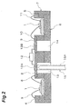
Fig. 2 is a longitudinal cross-sectional view similar toFig. 1 to show the state where a cooling head for forcibly cooling the P-pole bus bar and the N-pole bus bar shown inFig. 1 is inserted into one opening of the P-pole bus bar side. -
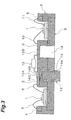
Fig. 3 is a longitudinal cross-sectional view similar toFig. 2 to show a modification of the cooling head shown inFig. 2 . - A preferable embodiment of a power module according to the invention will now be described with reference to the drawings. In the reference drawings,
Fig. 1 is a longitudinal cross-sectional view schematically showing the configuration of a power module according to an embodiment of the invention. - As shown in
Fig. 1 , the power module according to one embodiment of the invention includes a plurality ofswitching elements 1 constituting a bridge circuit, a P-pole bus bar 2 and an N-pole bus bar 3 for connecting therespective switching elements 1 to a power source, and anoutput bus bar 4 and anoutput bus bar 5 for extracting an output from therespective switching elements 1. - Each of the
switching elements 1 is constituted by an IGBT (Insulated Gate Bipolar Transistor) handling a large amount of power, in which an emitter E is stacked on a collector C. In this instance, a gate is not shown in the drawings. Theswitching elements 1 are respectively installed on aheat radiation plate 6 made of a thick plate in the vicinity of both right and left ends of the heat radiation plate. - The
heat radiation plate 6 is overmolded with aresin housing 7, except for an installed portion of therespective switching elements 1. The P-pole bus bar 2, the N-pole bus bar 3, theoutput bus bar 4 and theoutput bus bar 5 are respectively inserted into theresin housing 7 in one piece. - The P-
pole bus bar 2 and the N-pole bus bar 3 are made of, for example, a thick copper plate, and are arranged in a bilateral symmetry in the vicinity of a central portion of theresin housing 7 in a horizontal direction. Meanwhile, theoutput bus bar 4 and theoutput bus bar 5 are made of, for example, a copper rod of an angular shape, and are installed in the vicinity of both ends of theresin housing 7 in a horizontal direction thereof. - In the
switching element 1 disposed in the vicinity of the left end of theheat radiation plate 6, the collector C is electrically connected to the P-pole bus bar 2 via abonding wire 8, and the emitter E is electrically connected to theoutput bus bar 4 via abonding wire 9. - Meanwhile, in the switching
element 1 disposed in the vicinity of the right end of theheat radiation plate 6, the emitter E is electrically connected to the N-pole bus bar 3 via abonding wire 10, and the collector C is electrically connected to theoutput bus bar 5 via abonding wire 11. - Here, in order to suppress the surge voltage applied to the
respective switching elements 1, thesnubber capacitor 12 constituted by a ceramic capacitor having heat resistance is connected between the P-pole bus bar 2 and the N-pole bus bar 3. That is, onelead 12A of thesnubber capacitor 12 is later appended to an upper surface of a specific portion of the P-pole bus bar 2 by welding. In a similar fashion, theother lead 12B of thesnubber capacitor 12 is later appended to an upper surface of a specific portion of the N-pole bus bar 3 by welding. - As the configuration for this purpose, one
opening 13 is formed to extend over theheat radiation plate 6 and theresin housing 7 to expose the lower surface of the specific portion of the P-pole bus bar 2 and thus radiate the heat. In a similar fashion, theother opening 14 is formed to extend over theheat radiation plate 6 and theresin housing 7 to expose the lower surface of the specific portion of the N-pole bus bar 3 and thus radiate the heat. - Here, the one opening 13 and the
other opening 14 are respectively formed in the shape of a circular cross section, but the cross section is not limited to the circular shape. The cross section may assume other shape such as an oval or a rectangle. - In the power module including the above-described configuration according to the embodiment, for example, by electron beam welding, one
lead 12A of thesnubber capacitor 12 is welded to the upper surface of the P-pole bus bar 2, and theother lead 12B is welded to the upper surface of the specific portion of the N-pole bus bar 3. - In this instance, since the welding heat generated at the specific portion of the P-
pole bus bar 2 is radiated from the one opening 13 through which the lower surface of the specific portion of the P-pole bus bar 2 is exposed, theresin housing 7 in the vicinity of the P-pole bus bar 2 is not molten and damaged due to the welding heat. In a similar fashion, since the welding heat generated at the specific portion of the N-pole bus bar 3 is radiated from theother opening 14 through which the lower surface of the specific portion of the N-pole bus bar 3 is exposed, theresin housing 7 in the vicinity of the N-pole bus bar 3 is not molten and damaged due to the welding heat. - Therefore, with the power module according to the embodiment, it is possible to later append the
snubber capacitor 12 by welding without causing melting damage to theresin housing 7 by the welding heat. - Here, when the one lead 12A of the
snubber capacitor 12 is welded to the upper surface of the specific portion of the P-pole bus bar 2, if the lower surface of the specific portion of the P-pole bus bar 2 is forcibly cooled by a cooling head (cooling member) 15 shown inFig. 2 inserted into the one opening 13, it is possible to reliably avoid the melting damage to theresin housing 7 in the vicinity of the P-pole bus bar 2. - In a similar fashion, when the
other lead 12B of thesnubber capacitor 12 is welded to the upper surface of the specific portion of the N-pole bus bar 3, if the lower surface of the specific portion of the N-pole bus bar 3 is forcibly cooled by thecooling head 15 inserted into theother opening 14, it is possible to reliably avoid the melting damage to theresin housing 7 in the vicinity of the N-pole bus bar 3. - Here, the
cooling head 15 shown inFig. 2 has an external appearance formed in the shape of a rod having a small diameter, in which acirculation passage 15A for cooling water which is sent under pressure from a cooling device (not shown) is formed. An upper end surface of the cooling head is formed with a flat surface. - In this instance, the
cooling head 15 shown inFig. 2 may be changed into a cooling head (cooling member) 16 shown inFig. 3 . Thecooling head 16 has an external appearance formed in the shape of a rod having a small diameter, in which acirculation passage 16A for cooling water which is sent under pressure from a cooling device (not shown) is formed, similar to thecooling head 15 shown inFig. 2 , but the outer diameter of the cooling head is formed to have a large diameter slightly smaller than, for example, a diameter of the one opening 13. Thecooling head 16 is provided with a circular recessedportion 16B on a flat upper surface of thecooling head 16, and a ring-shaped cooling protrusion 16c is formed around the circular recessed portion. - Here, for example, with the
cooling head 16 inserted into the one opening 13 of the P-pole bus bar 2 side, the circular recessedportion 16B faces the lower surface of the specific portion of the P-pole bus bar 2 to which the one lead 12A of thesnubber capacitor 12 is welded, and thecooling protrusion 16C around the recessed portion forcibly cools the lower surface in the vicinity of the specific portion of the P-pole bus bar 2. - Accordingly, if the
cooling head 16 is used, the one lead 12A and theother lead 12B of thesnubber capacitor 12 can be reliably welded to the upper surface of the specific portions of the P-pole bus bar 2 and the N-pole bus bar 3, respectively. In addition, it is possible to reliably prevent theresin housing 7 in the vicinity of the P-pole bus bar 2 and the N-pole bus bar 3 from being molten and damaged. - According to the invention, when the lead of the snubber capacitor is welded to the upper surface of the specific portion of the bus bar, since the welding heat generated at the specific portion of the bus bar is radiated from the opening through which the lower surface of the specific portion of the bus bar is exposed, the snubber capacitor can be later appended to the bus bar by welding without causing the melting damage to the resin housing by the welding heat. Since the lower surface of the specific portion of the bus bar is forcibly cooled by the separate cooling member inserted into the opening during welding, it is possible to reliably avoid the melting damage to the resin housing.
Claims (1)
- A power module comprising:a bus bar that is inserted into a resin housing to connect a switching element to a power source; anda snubber capacitor that suppresses surge voltage of the switching element and has a lead welded to an upper surface of a specific portion of the bus bar,wherein at least the resin housing is provided with an opening, through which a lower surface of the specific portion of the bus bar is exposed.
Applications Claiming Priority (2)
| Application Number | Priority Date | Filing Date | Title |
|---|---|---|---|
| JP2007159243A JP4661830B2 (en) | 2007-06-15 | 2007-06-15 | Power module |
| PCT/JP2008/061181 WO2008153206A1 (en) | 2007-06-15 | 2008-06-12 | Power module |
Publications (3)
| Publication Number | Publication Date |
|---|---|
| EP2169718A1 true EP2169718A1 (en) | 2010-03-31 |
| EP2169718A4 EP2169718A4 (en) | 2011-01-05 |
| EP2169718B1 EP2169718B1 (en) | 2016-07-20 |
Family
ID=40129802
Family Applications (1)
| Application Number | Title | Priority Date | Filing Date |
|---|---|---|---|
| EP08777357.8A Not-in-force EP2169718B1 (en) | 2007-06-15 | 2008-06-12 | Power module |
Country Status (5)
| Country | Link |
|---|---|
| US (1) | US8254133B2 (en) |
| EP (1) | EP2169718B1 (en) |
| JP (1) | JP4661830B2 (en) |
| CN (1) | CN101681906B (en) |
| WO (1) | WO2008153206A1 (en) |
Families Citing this family (7)
| Publication number | Priority date | Publication date | Assignee | Title |
|---|---|---|---|---|
| US8897023B2 (en) * | 2009-05-15 | 2014-11-25 | Hamilton Sundstrand Corporation | Motor controller assembly with capacitor thermal isolation |
| US8547684B2 (en) * | 2009-12-17 | 2013-10-01 | Schneider Electric USA, Inc. | Panelboard having a parallel feeder bars distribution |
| JP5824672B2 (en) * | 2011-02-24 | 2015-11-25 | パナソニックIpマネジメント株式会社 | Power module |
| KR101204564B1 (en) * | 2011-09-30 | 2012-11-23 | 삼성전기주식회사 | Power Module Package And Method of Manufacturing The Same |
| CN107552909B (en) * | 2017-09-30 | 2020-07-17 | 无锡奥特维科技股份有限公司 | Bus bar welding method |
| JP6939542B2 (en) * | 2017-12-28 | 2021-09-22 | 株式会社オートネットワーク技術研究所 | Electrical connection device |
| JP7001960B2 (en) * | 2018-03-23 | 2022-01-20 | 株式会社オートネットワーク技術研究所 | Circuit configuration |
Family Cites Families (16)
| Publication number | Priority date | Publication date | Assignee | Title |
|---|---|---|---|---|
| WO1997001263A1 (en) * | 1995-06-20 | 1997-01-09 | Matsushita Electric Industrial Co., Ltd. | Part holder, substrate having same, and method of manufacturing same |
| US5943216A (en) * | 1997-06-03 | 1999-08-24 | Photo Opto Electronic Technologies | Apparatus for providing a two-sided, cavity, inverted-mounted component circuit board |
| CN2328048Y (en) * | 1997-10-30 | 1999-07-07 | 周立杰 | Special time delay socket for audio computer |
| JP2000058372A (en) * | 1998-08-04 | 2000-02-25 | Toshiba Corp | Ceramic capacitor mounting structure |
| JP3484122B2 (en) * | 2000-01-13 | 2004-01-06 | 三菱電機株式会社 | Power converter |
| JP4044265B2 (en) * | 2000-05-16 | 2008-02-06 | 三菱電機株式会社 | Power module |
| JP3698033B2 (en) * | 2000-08-22 | 2005-09-21 | 住友電装株式会社 | Junction box |
| JP2002134875A (en) * | 2000-10-26 | 2002-05-10 | Murata Mfg Co Ltd | Module component, packaging structure of it, and electronic device |
| JP2004096974A (en) * | 2002-09-04 | 2004-03-25 | Yaskawa Electric Corp | Snubber module and power converter |
| JP2004221256A (en) * | 2003-01-14 | 2004-08-05 | Auto Network Gijutsu Kenkyusho:Kk | Circuit structure and method of manufacturing the same |
| JP2005094882A (en) * | 2003-09-16 | 2005-04-07 | Toyota Motor Corp | Power module |
| JP4424042B2 (en) * | 2004-04-06 | 2010-03-03 | 住友電装株式会社 | Automotive relays and electrical junction boxes |
| JP4590961B2 (en) * | 2004-07-20 | 2010-12-01 | 株式会社デンソー | Electronic equipment |
| JP4430497B2 (en) | 2004-09-17 | 2010-03-10 | ニチコン株式会社 | Semiconductor module |
| JP4680816B2 (en) * | 2006-03-31 | 2011-05-11 | 三菱電機株式会社 | Semiconductor device |
| JP4635963B2 (en) * | 2006-06-02 | 2011-02-23 | 株式会社デンソー | Electrical circuit device |
-
2007
- 2007-06-15 JP JP2007159243A patent/JP4661830B2/en not_active Expired - Fee Related
-
2008
- 2008-06-12 CN CN2008800194495A patent/CN101681906B/en not_active Expired - Fee Related
- 2008-06-12 WO PCT/JP2008/061181 patent/WO2008153206A1/en not_active Ceased
- 2008-06-12 US US12/663,813 patent/US8254133B2/en not_active Expired - Fee Related
- 2008-06-12 EP EP08777357.8A patent/EP2169718B1/en not_active Not-in-force
Also Published As
| Publication number | Publication date |
|---|---|
| CN101681906A (en) | 2010-03-24 |
| JP2008311522A (en) | 2008-12-25 |
| CN101681906B (en) | 2011-03-30 |
| EP2169718A4 (en) | 2011-01-05 |
| US20100172117A1 (en) | 2010-07-08 |
| EP2169718B1 (en) | 2016-07-20 |
| WO2008153206A1 (en) | 2008-12-18 |
| US8254133B2 (en) | 2012-08-28 |
| JP4661830B2 (en) | 2011-03-30 |
Similar Documents
| Publication | Publication Date | Title |
|---|---|---|
| EP2169718B1 (en) | Power module | |
| CN109698179B (en) | Semiconductor device and method for manufacturing semiconductor device | |
| JP2007035670A (en) | Semiconductor device | |
| JP6610101B2 (en) | Semiconductor module | |
| CN110771027B (en) | Power semiconductor device and power conversion device using the same | |
| JP6343249B2 (en) | Controller and controller manufacturing method | |
| JP6354283B2 (en) | Semiconductor module and semiconductor device | |
| JP6165689B2 (en) | Power semiconductor module | |
| JP2009027778A (en) | Bus bar | |
| US12074097B2 (en) | Power module | |
| EP2077579A1 (en) | Twin chip-mounted diode | |
| JP6365322B2 (en) | Semiconductor device | |
| JP6192809B2 (en) | Semiconductor module and drive device mounted with semiconductor module | |
| JP5781185B1 (en) | Resin-sealed semiconductor device | |
| JP2018081980A (en) | Semiconductor device | |
| JP5217015B2 (en) | Power converter and manufacturing method thereof | |
| JP6580015B2 (en) | Molded resin encapsulated power semiconductor device | |
| CN108496247A (en) | Semiconductor device | |
| US20170170150A1 (en) | Semiconductor module and semiconductor device | |
| CN114823636A (en) | Semiconductor module | |
| WO2019163941A1 (en) | Substrate for power modules, and power module | |
| JP4349364B2 (en) | Semiconductor device | |
| JP2015149363A (en) | Semiconductor module | |
| JP2021061263A (en) | Semiconductor unit and semiconductor device | |
| JP2019021831A (en) | Semiconductor device and submodule for semiconductor device |
Legal Events
| Date | Code | Title | Description |
|---|---|---|---|
| PUAI | Public reference made under article 153(3) epc to a published international application that has entered the european phase |
Free format text: ORIGINAL CODE: 0009012 |
|
| 17P | Request for examination filed |
Effective date: 20100105 |
|
| AK | Designated contracting states |
Kind code of ref document: A1 Designated state(s): AT BE BG CH CY CZ DE DK EE ES FI FR GB GR HR HU IE IS IT LI LT LU LV MC MT NL NO PL PT RO SE SI SK TR |
|
| AX | Request for extension of the european patent |
Extension state: AL BA MK RS |
|
| DAX | Request for extension of the european patent (deleted) | ||
| A4 | Supplementary search report drawn up and despatched |
Effective date: 20101206 |
|
| RIC1 | Information provided on ipc code assigned before grant |
Ipc: H01L 25/16 20060101ALI20101130BHEP Ipc: H01L 25/07 20060101AFI20090108BHEP Ipc: H01L 25/18 20060101ALI20101130BHEP |
|
| RAP1 | Party data changed (applicant data changed or rights of an application transferred) |
Owner name: TOYOTA JIDOSHA KABUSHIKI KAISHA |
|
| 17Q | First examination report despatched |
Effective date: 20140211 |
|
| REG | Reference to a national code |
Ref country code: DE Ref legal event code: R079 Ref document number: 602008045209 Country of ref document: DE Free format text: PREVIOUS MAIN CLASS: H01L0025070000 Ipc: H01L0023040000 |
|
| RIC1 | Information provided on ipc code assigned before grant |
Ipc: H01L 25/07 20060101ALN20151218BHEP Ipc: H01L 23/473 20060101ALI20151218BHEP Ipc: H01L 23/04 20060101AFI20151218BHEP |
|
| GRAP | Despatch of communication of intention to grant a patent |
Free format text: ORIGINAL CODE: EPIDOSNIGR1 |
|
| INTG | Intention to grant announced |
Effective date: 20160202 |
|
| GRAS | Grant fee paid |
Free format text: ORIGINAL CODE: EPIDOSNIGR3 |
|
| GRAA | (expected) grant |
Free format text: ORIGINAL CODE: 0009210 |
|
| AK | Designated contracting states |
Kind code of ref document: B1 Designated state(s): AT BE BG CH CY CZ DE DK EE ES FI FR GB GR HR HU IE IS IT LI LT LU LV MC MT NL NO PL PT RO SE SI SK TR |
|
| REG | Reference to a national code |
Ref country code: GB Ref legal event code: FG4D |
|
| REG | Reference to a national code |
Ref country code: CH Ref legal event code: EP |
|
| REG | Reference to a national code |
Ref country code: IE Ref legal event code: FG4D |
|
| REG | Reference to a national code |
Ref country code: AT Ref legal event code: REF Ref document number: 814684 Country of ref document: AT Kind code of ref document: T Effective date: 20160815 |
|
| REG | Reference to a national code |
Ref country code: DE Ref legal event code: R096 Ref document number: 602008045209 Country of ref document: DE |
|
| REG | Reference to a national code |
Ref country code: LT Ref legal event code: MG4D |
|
| REG | Reference to a national code |
Ref country code: NL Ref legal event code: MP Effective date: 20160720 |
|
| REG | Reference to a national code |
Ref country code: AT Ref legal event code: MK05 Ref document number: 814684 Country of ref document: AT Kind code of ref document: T Effective date: 20160720 |
|
| PG25 | Lapsed in a contracting state [announced via postgrant information from national office to epo] |
Ref country code: IT Free format text: LAPSE BECAUSE OF FAILURE TO SUBMIT A TRANSLATION OF THE DESCRIPTION OR TO PAY THE FEE WITHIN THE PRESCRIBED TIME-LIMIT Effective date: 20160720 Ref country code: LT Free format text: LAPSE BECAUSE OF FAILURE TO SUBMIT A TRANSLATION OF THE DESCRIPTION OR TO PAY THE FEE WITHIN THE PRESCRIBED TIME-LIMIT Effective date: 20160720 Ref country code: FI Free format text: LAPSE BECAUSE OF FAILURE TO SUBMIT A TRANSLATION OF THE DESCRIPTION OR TO PAY THE FEE WITHIN THE PRESCRIBED TIME-LIMIT Effective date: 20160720 Ref country code: HR Free format text: LAPSE BECAUSE OF FAILURE TO SUBMIT A TRANSLATION OF THE DESCRIPTION OR TO PAY THE FEE WITHIN THE PRESCRIBED TIME-LIMIT Effective date: 20160720 Ref country code: IS Free format text: LAPSE BECAUSE OF FAILURE TO SUBMIT A TRANSLATION OF THE DESCRIPTION OR TO PAY THE FEE WITHIN THE PRESCRIBED TIME-LIMIT Effective date: 20161120 Ref country code: NL Free format text: LAPSE BECAUSE OF FAILURE TO SUBMIT A TRANSLATION OF THE DESCRIPTION OR TO PAY THE FEE WITHIN THE PRESCRIBED TIME-LIMIT Effective date: 20160720 Ref country code: NO Free format text: LAPSE BECAUSE OF FAILURE TO SUBMIT A TRANSLATION OF THE DESCRIPTION OR TO PAY THE FEE WITHIN THE PRESCRIBED TIME-LIMIT Effective date: 20161020 |
|
| PG25 | Lapsed in a contracting state [announced via postgrant information from national office to epo] |
Ref country code: PL Free format text: LAPSE BECAUSE OF FAILURE TO SUBMIT A TRANSLATION OF THE DESCRIPTION OR TO PAY THE FEE WITHIN THE PRESCRIBED TIME-LIMIT Effective date: 20160720 Ref country code: ES Free format text: LAPSE BECAUSE OF FAILURE TO SUBMIT A TRANSLATION OF THE DESCRIPTION OR TO PAY THE FEE WITHIN THE PRESCRIBED TIME-LIMIT Effective date: 20160720 Ref country code: BE Free format text: LAPSE BECAUSE OF FAILURE TO SUBMIT A TRANSLATION OF THE DESCRIPTION OR TO PAY THE FEE WITHIN THE PRESCRIBED TIME-LIMIT Effective date: 20160720 Ref country code: AT Free format text: LAPSE BECAUSE OF FAILURE TO SUBMIT A TRANSLATION OF THE DESCRIPTION OR TO PAY THE FEE WITHIN THE PRESCRIBED TIME-LIMIT Effective date: 20160720 Ref country code: SE Free format text: LAPSE BECAUSE OF FAILURE TO SUBMIT A TRANSLATION OF THE DESCRIPTION OR TO PAY THE FEE WITHIN THE PRESCRIBED TIME-LIMIT Effective date: 20160720 Ref country code: GR Free format text: LAPSE BECAUSE OF FAILURE TO SUBMIT A TRANSLATION OF THE DESCRIPTION OR TO PAY THE FEE WITHIN THE PRESCRIBED TIME-LIMIT Effective date: 20161021 Ref country code: PT Free format text: LAPSE BECAUSE OF FAILURE TO SUBMIT A TRANSLATION OF THE DESCRIPTION OR TO PAY THE FEE WITHIN THE PRESCRIBED TIME-LIMIT Effective date: 20161121 Ref country code: LV Free format text: LAPSE BECAUSE OF FAILURE TO SUBMIT A TRANSLATION OF THE DESCRIPTION OR TO PAY THE FEE WITHIN THE PRESCRIBED TIME-LIMIT Effective date: 20160720 |
|
| REG | Reference to a national code |
Ref country code: DE Ref legal event code: R084 Ref document number: 602008045209 Country of ref document: DE |
|
| REG | Reference to a national code |
Ref country code: DE Ref legal event code: R097 Ref document number: 602008045209 Country of ref document: DE |
|
| PG25 | Lapsed in a contracting state [announced via postgrant information from national office to epo] |
Ref country code: RO Free format text: LAPSE BECAUSE OF FAILURE TO SUBMIT A TRANSLATION OF THE DESCRIPTION OR TO PAY THE FEE WITHIN THE PRESCRIBED TIME-LIMIT Effective date: 20160720 Ref country code: EE Free format text: LAPSE BECAUSE OF FAILURE TO SUBMIT A TRANSLATION OF THE DESCRIPTION OR TO PAY THE FEE WITHIN THE PRESCRIBED TIME-LIMIT Effective date: 20160720 |
|
| PLBE | No opposition filed within time limit |
Free format text: ORIGINAL CODE: 0009261 |
|
| STAA | Information on the status of an ep patent application or granted ep patent |
Free format text: STATUS: NO OPPOSITION FILED WITHIN TIME LIMIT |
|
| PG25 | Lapsed in a contracting state [announced via postgrant information from national office to epo] |
Ref country code: DK Free format text: LAPSE BECAUSE OF FAILURE TO SUBMIT A TRANSLATION OF THE DESCRIPTION OR TO PAY THE FEE WITHIN THE PRESCRIBED TIME-LIMIT Effective date: 20160720 Ref country code: BG Free format text: LAPSE BECAUSE OF FAILURE TO SUBMIT A TRANSLATION OF THE DESCRIPTION OR TO PAY THE FEE WITHIN THE PRESCRIBED TIME-LIMIT Effective date: 20161020 Ref country code: CZ Free format text: LAPSE BECAUSE OF FAILURE TO SUBMIT A TRANSLATION OF THE DESCRIPTION OR TO PAY THE FEE WITHIN THE PRESCRIBED TIME-LIMIT Effective date: 20160720 Ref country code: SK Free format text: LAPSE BECAUSE OF FAILURE TO SUBMIT A TRANSLATION OF THE DESCRIPTION OR TO PAY THE FEE WITHIN THE PRESCRIBED TIME-LIMIT Effective date: 20160720 |
|
| 26N | No opposition filed |
Effective date: 20170421 |
|
| PG25 | Lapsed in a contracting state [announced via postgrant information from national office to epo] |
Ref country code: SI Free format text: LAPSE BECAUSE OF FAILURE TO SUBMIT A TRANSLATION OF THE DESCRIPTION OR TO PAY THE FEE WITHIN THE PRESCRIBED TIME-LIMIT Effective date: 20160720 |
|
| PG25 | Lapsed in a contracting state [announced via postgrant information from national office to epo] |
Ref country code: MC Free format text: LAPSE BECAUSE OF FAILURE TO SUBMIT A TRANSLATION OF THE DESCRIPTION OR TO PAY THE FEE WITHIN THE PRESCRIBED TIME-LIMIT Effective date: 20160720 |
|
| REG | Reference to a national code |
Ref country code: CH Ref legal event code: PL |
|
| GBPC | Gb: european patent ceased through non-payment of renewal fee |
Effective date: 20170612 |
|
| REG | Reference to a national code |
Ref country code: IE Ref legal event code: MM4A |
|
| REG | Reference to a national code |
Ref country code: FR Ref legal event code: ST Effective date: 20180228 |
|
| PG25 | Lapsed in a contracting state [announced via postgrant information from national office to epo] |
Ref country code: IE Free format text: LAPSE BECAUSE OF NON-PAYMENT OF DUE FEES Effective date: 20170612 Ref country code: LI Free format text: LAPSE BECAUSE OF NON-PAYMENT OF DUE FEES Effective date: 20170630 Ref country code: LU Free format text: LAPSE BECAUSE OF NON-PAYMENT OF DUE FEES Effective date: 20170612 Ref country code: CH Free format text: LAPSE BECAUSE OF NON-PAYMENT OF DUE FEES Effective date: 20170630 Ref country code: GB Free format text: LAPSE BECAUSE OF NON-PAYMENT OF DUE FEES Effective date: 20170612 |
|
| PG25 | Lapsed in a contracting state [announced via postgrant information from national office to epo] |
Ref country code: FR Free format text: LAPSE BECAUSE OF NON-PAYMENT OF DUE FEES Effective date: 20170630 |
|
| PG25 | Lapsed in a contracting state [announced via postgrant information from national office to epo] |
Ref country code: MT Free format text: LAPSE BECAUSE OF NON-PAYMENT OF DUE FEES Effective date: 20170612 |
|
| PG25 | Lapsed in a contracting state [announced via postgrant information from national office to epo] |
Ref country code: HU Free format text: LAPSE BECAUSE OF FAILURE TO SUBMIT A TRANSLATION OF THE DESCRIPTION OR TO PAY THE FEE WITHIN THE PRESCRIBED TIME-LIMIT; INVALID AB INITIO Effective date: 20080612 |
|
| PG25 | Lapsed in a contracting state [announced via postgrant information from national office to epo] |
Ref country code: CY Free format text: LAPSE BECAUSE OF NON-PAYMENT OF DUE FEES Effective date: 20160720 |
|
| PG25 | Lapsed in a contracting state [announced via postgrant information from national office to epo] |
Ref country code: TR Free format text: LAPSE BECAUSE OF FAILURE TO SUBMIT A TRANSLATION OF THE DESCRIPTION OR TO PAY THE FEE WITHIN THE PRESCRIBED TIME-LIMIT Effective date: 20160720 |
|
| PGFP | Annual fee paid to national office [announced via postgrant information from national office to epo] |
Ref country code: DE Payment date: 20200602 Year of fee payment: 13 |
|
| REG | Reference to a national code |
Ref country code: DE Ref legal event code: R119 Ref document number: 602008045209 Country of ref document: DE |
|
| PG25 | Lapsed in a contracting state [announced via postgrant information from national office to epo] |
Ref country code: DE Free format text: LAPSE BECAUSE OF NON-PAYMENT OF DUE FEES Effective date: 20220101 |