EP2165241B1 - Method of adapting the stray light of a projection objective for microlithography - Google Patents
Method of adapting the stray light of a projection objective for microlithography Download PDFInfo
- Publication number
- EP2165241B1 EP2165241B1 EP08784500A EP08784500A EP2165241B1 EP 2165241 B1 EP2165241 B1 EP 2165241B1 EP 08784500 A EP08784500 A EP 08784500A EP 08784500 A EP08784500 A EP 08784500A EP 2165241 B1 EP2165241 B1 EP 2165241B1
- Authority
- EP
- European Patent Office
- Prior art keywords
- stray light
- field
- light component
- projection objective
- plane
- Prior art date
- Legal status (The legal status is an assumption and is not a legal conclusion. Google has not performed a legal analysis and makes no representation as to the accuracy of the status listed.)
- Not-in-force
Links
Images


Classifications
-
- G—PHYSICS
- G03—PHOTOGRAPHY; CINEMATOGRAPHY; ANALOGOUS TECHNIQUES USING WAVES OTHER THAN OPTICAL WAVES; ELECTROGRAPHY; HOLOGRAPHY
- G03F—PHOTOMECHANICAL PRODUCTION OF TEXTURED OR PATTERNED SURFACES, e.g. FOR PRINTING, FOR PROCESSING OF SEMICONDUCTOR DEVICES; MATERIALS THEREFOR; ORIGINALS THEREFOR; APPARATUS SPECIALLY ADAPTED THEREFOR
- G03F7/00—Photomechanical, e.g. photolithographic, production of textured or patterned surfaces, e.g. printing surfaces; Materials therefor, e.g. comprising photoresists; Apparatus specially adapted therefor
- G03F7/70—Microphotolithographic exposure; Apparatus therefor
- G03F7/708—Construction of apparatus, e.g. environment aspects, hygiene aspects or materials
- G03F7/7095—Materials, e.g. materials for housing, stage or other support having particular properties, e.g. weight, strength, conductivity, thermal expansion coefficient
- G03F7/70958—Optical materials or coatings, e.g. with particular transmittance, reflectance or anti-reflection properties
-
- G—PHYSICS
- G03—PHOTOGRAPHY; CINEMATOGRAPHY; ANALOGOUS TECHNIQUES USING WAVES OTHER THAN OPTICAL WAVES; ELECTROGRAPHY; HOLOGRAPHY
- G03F—PHOTOMECHANICAL PRODUCTION OF TEXTURED OR PATTERNED SURFACES, e.g. FOR PRINTING, FOR PROCESSING OF SEMICONDUCTOR DEVICES; MATERIALS THEREFOR; ORIGINALS THEREFOR; APPARATUS SPECIALLY ADAPTED THEREFOR
- G03F7/00—Photomechanical, e.g. photolithographic, production of textured or patterned surfaces, e.g. printing surfaces; Materials therefor, e.g. comprising photoresists; Apparatus specially adapted therefor
- G03F7/70—Microphotolithographic exposure; Apparatus therefor
- G03F7/70216—Mask projection systems
- G03F7/70308—Optical correction elements, filters or phase plates for manipulating imaging light, e.g. intensity, wavelength, polarisation, phase or image shift
-
- G—PHYSICS
- G03—PHOTOGRAPHY; CINEMATOGRAPHY; ANALOGOUS TECHNIQUES USING WAVES OTHER THAN OPTICAL WAVES; ELECTROGRAPHY; HOLOGRAPHY
- G03F—PHOTOMECHANICAL PRODUCTION OF TEXTURED OR PATTERNED SURFACES, e.g. FOR PRINTING, FOR PROCESSING OF SEMICONDUCTOR DEVICES; MATERIALS THEREFOR; ORIGINALS THEREFOR; APPARATUS SPECIALLY ADAPTED THEREFOR
- G03F7/00—Photomechanical, e.g. photolithographic, production of textured or patterned surfaces, e.g. printing surfaces; Materials therefor, e.g. comprising photoresists; Apparatus specially adapted therefor
- G03F7/70—Microphotolithographic exposure; Apparatus therefor
- G03F7/70216—Mask projection systems
- G03F7/70275—Multiple projection paths, e.g. array of projection systems, microlens projection systems or tandem projection systems
-
- G—PHYSICS
- G03—PHOTOGRAPHY; CINEMATOGRAPHY; ANALOGOUS TECHNIQUES USING WAVES OTHER THAN OPTICAL WAVES; ELECTROGRAPHY; HOLOGRAPHY
- G03F—PHOTOMECHANICAL PRODUCTION OF TEXTURED OR PATTERNED SURFACES, e.g. FOR PRINTING, FOR PROCESSING OF SEMICONDUCTOR DEVICES; MATERIALS THEREFOR; ORIGINALS THEREFOR; APPARATUS SPECIALLY ADAPTED THEREFOR
- G03F7/00—Photomechanical, e.g. photolithographic, production of textured or patterned surfaces, e.g. printing surfaces; Materials therefor, e.g. comprising photoresists; Apparatus specially adapted therefor
- G03F7/70—Microphotolithographic exposure; Apparatus therefor
- G03F7/70216—Mask projection systems
- G03F7/70341—Details of immersion lithography aspects, e.g. exposure media or control of immersion liquid supply
-
- G—PHYSICS
- G03—PHOTOGRAPHY; CINEMATOGRAPHY; ANALOGOUS TECHNIQUES USING WAVES OTHER THAN OPTICAL WAVES; ELECTROGRAPHY; HOLOGRAPHY
- G03F—PHOTOMECHANICAL PRODUCTION OF TEXTURED OR PATTERNED SURFACES, e.g. FOR PRINTING, FOR PROCESSING OF SEMICONDUCTOR DEVICES; MATERIALS THEREFOR; ORIGINALS THEREFOR; APPARATUS SPECIALLY ADAPTED THEREFOR
- G03F7/00—Photomechanical, e.g. photolithographic, production of textured or patterned surfaces, e.g. printing surfaces; Materials therefor, e.g. comprising photoresists; Apparatus specially adapted therefor
- G03F7/70—Microphotolithographic exposure; Apparatus therefor
- G03F7/70483—Information management; Active and passive control; Testing; Wafer monitoring, e.g. pattern monitoring
- G03F7/70591—Testing optical components
-
- G—PHYSICS
- G03—PHOTOGRAPHY; CINEMATOGRAPHY; ANALOGOUS TECHNIQUES USING WAVES OTHER THAN OPTICAL WAVES; ELECTROGRAPHY; HOLOGRAPHY
- G03F—PHOTOMECHANICAL PRODUCTION OF TEXTURED OR PATTERNED SURFACES, e.g. FOR PRINTING, FOR PROCESSING OF SEMICONDUCTOR DEVICES; MATERIALS THEREFOR; ORIGINALS THEREFOR; APPARATUS SPECIALLY ADAPTED THEREFOR
- G03F7/00—Photomechanical, e.g. photolithographic, production of textured or patterned surfaces, e.g. printing surfaces; Materials therefor, e.g. comprising photoresists; Apparatus specially adapted therefor
- G03F7/70—Microphotolithographic exposure; Apparatus therefor
- G03F7/708—Construction of apparatus, e.g. environment aspects, hygiene aspects or materials
- G03F7/70908—Hygiene, e.g. preventing apparatus pollution, mitigating effect of pollution or removing pollutants from apparatus
- G03F7/70941—Stray fields and charges, e.g. stray light, scattered light, flare, transmission loss
Definitions
- the stray light component of an objective has different reasons, which are described in: Heinz Haferkorn, "Optik; Physikalisch-technische Kunststoffn und füren” (Optics, Physical and Technical Theory and Applications), Fourth Revised and Expanded Edition; Verlag WileY-VCH, Weinheim; pages 690-694 .
- Optik Optik
- Physikalisch-technische Kunststoffn und füren Optics, Physical and Technical Theory and Applications
- Verlag WileY-VCH, Weinheim pages 690-694 .
- the kind of stray light which is caused by the scattering of light at inhomogeneities within a transparent optical material
- the kind of stray light which is caused by the scattering of light at irregularities of the surfaces of the optical elements.
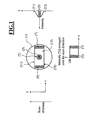
- the illumination system is capable of changing the angular distribution of the incident light rays 107 falling homogeneously on the mask 101, without thereby changing the intensity distribution over the mask. This makes it possible to have different so-called settings available for the semiconductor manufacturer, which can be described in terms of the theory of partially coherent images and which have the purpose that certain structures on the mask 101 can be projected into the smallest possible image size.
- the principal rays 139, 149 of the field points thus have no height, or distance from the optical axis, in the pupil.
- the aperture rays 141, 143 define the border of the pupil and thus have the maximum height, or maximum distance from the optical axis, of all possible rays in the pupil.
- the height, or distance from the optical axis, of the rays thus represents a suitable criterion as to whether an optical element in an objective can be referred to as being near a pupil (pupil-proximate) or near a field (field-proximate).
- the angle between the image-forming ray 139, 141, 143, 149 and the optical axis in the field corresponds to the height, or distance from the optical axis 131, of the image-forming ray 139, 141, 143, 149 in the field.
- the path of the principal ray 149 of the outermost field point that can be projected has its maximum height, or greatest distance from the optical axis 131, in the image plane of the mask 121, with an angle of zero relative to the optical axis 131.
- the same ray path 149 crosses the optical axis 131 at the center of the pupil plane 133 with the maximum angle of intersection, i.e.
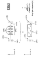
- Figure 12 represents a sketch to illustrate principal concepts regarding the scattering at inhomogeneities 407 in the polycrystalline material of a last lens 400 and regarding the concept of adapting the surface roughness 403 of a last lens, as well as the resultant stray light distributions 411, 413 over the field.
- a last lens 400 of a projection objective is located before the field plane 405 which extends perpendicular to the optical axis 401 immediately after the last lens 400.
- the inhomogeneities of the glass material are symbolically indicated in the lens 400 as scatter lobes 407 which represent the angular distribution of the stray light.
- the stray light component 411 of the lens 400 due to the inhomogeneities of the glass material (volume scatter), averaged over the scan direction and expressed as a percentage relative to the useful light is shown in the midportion of Figure 12 as a profile graph over the field along the X-direction.
- the invention is suited insofar not only for the correction of projection objectives with a last lens of polycrystalline material, but also for the improvement of current projection objectives so that they will have a constant stray light component with less than 0.2% variation over the exposure field.
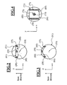
- the mask plane 2101 is projected by the first refractive objective group 2110 onto an extended intermediate image plane 2103.
- the first refractive group has a pupil- or aperture plane A.
- the mirror group 2120 with the mirrors 2121 and 2122 projects the extended intermediate image plane 2103 into a further extended intermediate image plane 2104.
- the second refractive objective group 2130 projects the extended intermediate image plane 2104 into the field plane 2102.
- the last lens before the field plane 2102 in the direction of the light rays from the mask plane 2101 to the field plane 2102 carries the reference symbol 2150.
- Figure 18 shows as a detail of the design 800 of Figure 17 the last lens element LOE before the field plane IP in the direction of the light rays from the mask plane OP to the image plane IP.
- This lens element consists of quartz glass for the partial lens LOE1 and sapphire for the partial lens LOE2, wherein the crystallographic axis in the latter is oriented in the direction CA parallel to the optical axis AX. Between the two partial lenses LOE1 and LOE2 there is an immersion liquid.
- crystalline materials with a high index of refraction are also mentioned in WO 2005/133801 A1 for the second partial lens LOE2, such as for example spinel (MgAl 2 O 4 ), YAG [yttrium aluminum garnet (Y 3 Al 5 O 12 )], magnesium oxide (MgO), beryllium oxide (BeO), aluminum oxide (Al 2 O 3 ), yttrium oxide (Y 2 O 3 ) or lanthanum fluoride (LaF 3 ).
- spinel MgAl 2 O 4
- YAG yttrium aluminum garnet (Y 3 Al 5 O 12 )
- magnesium oxide MgO
- BeO beryllium oxide
- Al 2 O 3 aluminum oxide
- Y 2 O 3 yttrium oxide
- LaF 3 lanthanum fluoride
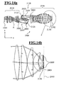
- Figure 21 schematically illustrates the different methods whereby it is possible to provide a projection objective for applications in the field of microlithography with an additional stray light component, averaged over the scan direction, whose profile over the exposure field is such that the stray light component of the projection objective, averaged in the scan direction, has a reduced variation over the exposure field or, more specifically, that a stray light component of a projection objective, averaged in the scan direction, is obtained which is constant in the sense of this patent application.
- the stray light component of the projection objective is either simulated or determined from data of the components or data of the respective blanks.
- the success of the measures taken in the second step is verified in a third step by a measurement which is taken as part of a qualifying examination of the projection objective.
- the projection objective is either accepted as having a sufficiently good correction, or the process loops back to the second step, wherein the surface roughness of the surface of the field-proximate element or of the surfaces of the field-proximate elements is changed from its previous value.
Landscapes
- Physics & Mathematics (AREA)
- General Physics & Mathematics (AREA)
- Epidemiology (AREA)
- Health & Medical Sciences (AREA)
- Public Health (AREA)
- Environmental & Geological Engineering (AREA)
- Engineering & Computer Science (AREA)
- Life Sciences & Earth Sciences (AREA)
- Atmospheric Sciences (AREA)
- Exposure And Positioning Against Photoresist Photosensitive Materials (AREA)
- Lenses (AREA)
- Exposure Of Semiconductors, Excluding Electron Or Ion Beam Exposure (AREA)
- Diffracting Gratings Or Hologram Optical Elements (AREA)
- Holo Graphy (AREA)
- Polarising Elements (AREA)
Applications Claiming Priority (3)
| Application Number | Priority Date | Filing Date | Title |
|---|---|---|---|
| US94011707P | 2007-05-25 | 2007-05-25 | |
| DE102007024685 | 2007-05-25 | ||
| PCT/EP2008/004084 WO2008145296A1 (en) | 2007-05-25 | 2008-05-21 | Projection objective for microlithography, microlithography projection exposure apparatus with said projection objective, microlithographic manufacturing method for components, as well as a component manufactured with said method |
Publications (2)
| Publication Number | Publication Date |
|---|---|
| EP2165241A1 EP2165241A1 (en) | 2010-03-24 |
| EP2165241B1 true EP2165241B1 (en) | 2013-02-27 |
Family
ID=39877324
Family Applications (1)
| Application Number | Title | Priority Date | Filing Date |
|---|---|---|---|
| EP08784500A Not-in-force EP2165241B1 (en) | 2007-05-25 | 2008-05-21 | Method of adapting the stray light of a projection objective for microlithography |
Country Status (8)
| Country | Link |
|---|---|
| US (2) | US9063439B2 (enExample) |
| EP (1) | EP2165241B1 (enExample) |
| JP (2) | JP4968558B2 (enExample) |
| KR (1) | KR101544224B1 (enExample) |
| CN (1) | CN101689027B (enExample) |
| DE (1) | DE102008001800A1 (enExample) |
| TW (1) | TWI483081B (enExample) |
| WO (2) | WO2008145296A1 (enExample) |
Families Citing this family (19)
| Publication number | Priority date | Publication date | Assignee | Title |
|---|---|---|---|---|
| US9188874B1 (en) | 2011-05-09 | 2015-11-17 | Kenneth C. Johnson | Spot-array imaging system for maskless lithography and parallel confocal microscopy |
| US8994920B1 (en) | 2010-05-07 | 2015-03-31 | Kenneth C. Johnson | Optical systems and methods for absorbance modulation |
| WO2015012982A1 (en) * | 2013-07-22 | 2015-01-29 | Johnson Kenneth C | Scanned-spot-array duv lithography system |
| US9097983B2 (en) | 2011-05-09 | 2015-08-04 | Kenneth C. Johnson | Scanned-spot-array EUV lithography system |
| DE102008001800A1 (de) * | 2007-05-25 | 2008-11-27 | Carl Zeiss Smt Ag | Projektionsobjektiv für die Mikrolithographie, Mikrolithographie-Projektionsbelichtungsanlage mit einem derartigen Projektionsobjektiv, mikrolithographisches Herstellungsverfahren für Bauelemente sowie mit diesem Verfahren hergestelltes Bauelement |
| CN101849210B (zh) * | 2007-11-08 | 2012-11-14 | Asml荷兰有限公司 | 光刻投影设备和补偿扰动因素的方法 |
| DE102008043324B4 (de) * | 2008-10-30 | 2010-11-11 | Carl Zeiss Smt Ag | Optische Anordnung zur dreidimensionalen Strukturierung einer Materialschicht |
| EP2219077A1 (en) | 2009-02-12 | 2010-08-18 | Carl Zeiss SMT AG | Projection exposure method, projection exposure system and projection objective |
| US20110094123A1 (en) * | 2009-10-28 | 2011-04-28 | Richard Vaughn | Fabric-covered fluid-filled therapeutic foot orthotic with thong-cut device systems |
| US8443308B2 (en) * | 2011-05-02 | 2013-05-14 | Synopsys Inc. | EUV lithography flare calculation and compensation |
| DE102012112773B4 (de) * | 2012-12-20 | 2020-04-30 | Jenoptik Optical Systems Gmbh | Verfahren zur Herstellung einer wellenfrontkorrigierten optischen Anordnung aus mindestens zwei optischen Elementen und Verwendung des Verfahrens |
| US9857570B1 (en) * | 2014-07-24 | 2018-01-02 | Hoyos Integrity Corporation | Full flat mirror guiding reflections to aperture of panoramic optical device |
| CN104317168B (zh) * | 2014-10-28 | 2016-03-02 | 中国科学院长春光学精密机械与物理研究所 | 极紫外光刻系统中与杂散光有关的镜面加工误差分析方法 |
| US10098529B2 (en) * | 2015-10-28 | 2018-10-16 | Ricoh Company, Ltd. | Optical design of a light field otoscope |
| US20170119237A1 (en) * | 2015-10-28 | 2017-05-04 | Ricoh Company, Ltd. | Optical Design of a Light Field Otoscope |
| US10417533B2 (en) * | 2016-08-09 | 2019-09-17 | Cognex Corporation | Selection of balanced-probe sites for 3-D alignment algorithms |
| CN106773555B (zh) * | 2017-03-21 | 2019-03-26 | 上海华力微电子有限公司 | 补偿由光刻镜头散射光导致曝光误差的方法 |
| CN112034605B (zh) * | 2020-09-09 | 2025-01-24 | 苏州大学 | 一种折反式Golay3稀疏孔径光学系统 |
| CN119270401A (zh) * | 2023-07-07 | 2025-01-07 | 玉晶光电(厦门)有限公司 | 一种使杂散光多次反射的光学元件 |
Family Cites Families (20)
| Publication number | Priority date | Publication date | Assignee | Title |
|---|---|---|---|---|
| US6985210B2 (en) | 1999-02-15 | 2006-01-10 | Carl Zeiss Smt Ag | Projection system for EUV lithography |
| JP2001264626A (ja) | 2000-03-15 | 2001-09-26 | Canon Inc | 回折光学素子を有する光学系 |
| JP2002353094A (ja) * | 2001-05-22 | 2002-12-06 | Nikon Corp | 照明光学装置および露光装置 |
| JP3679736B2 (ja) * | 2001-07-04 | 2005-08-03 | キヤノン株式会社 | 露光装置、露光方法、デバイス製造方法、並びに、デバイス |
| JP2004004601A (ja) * | 2002-04-04 | 2004-01-08 | Sony Corp | 光スイッチング素子、光スイッチング素子アレイ、及び画像表示装置 |
| JP2003318095A (ja) * | 2002-04-24 | 2003-11-07 | Nikon Corp | フレア計測方法及びフレア計測装置、露光方法及び露光装置、露光装置の調整方法 |
| JP2005536775A (ja) | 2002-08-23 | 2005-12-02 | 株式会社ニコン | 投影光学系、フォトリソグラフィ方法および露光装置、並びに露光装置を用いた方法 |
| US7348575B2 (en) | 2003-05-06 | 2008-03-25 | Nikon Corporation | Projection optical system, exposure apparatus, and exposure method |
| AU2003267402A1 (en) | 2003-08-04 | 2005-02-25 | Carl Zeiss Smt Ag | Illumination mask for range-resolved detection of scattered light |
| JP2005134666A (ja) * | 2003-10-30 | 2005-05-26 | Hoya Corp | フォトマスク及び映像デバイスの製造方法 |
| US7466489B2 (en) | 2003-12-15 | 2008-12-16 | Susanne Beder | Projection objective having a high aperture and a planar end surface |
| KR101407204B1 (ko) | 2004-01-14 | 2014-06-13 | 칼 짜이스 에스엠티 게엠베하 | 투영 대물렌즈 |
| JP2006120899A (ja) * | 2004-10-22 | 2006-05-11 | Nikon Corp | 投影光学系、投影光学系の調整方法、投影露光装置、投影露光方法、および投影露光装置の調整方法 |
| EP1820050A1 (en) | 2004-12-09 | 2007-08-22 | Carl Zeiss SMT AG | Transmitting optical element and objective for a microlithographic projection exposure apparatus |
| EP1669196B1 (en) | 2004-12-10 | 2008-05-21 | ESSILOR INTERNATIONAL (Compagnie Générale d'Optique) | Stamp for patterning, method for manufacturing such stamp and method for manufacturing an object using the stamp. |
| US7125178B2 (en) | 2004-12-22 | 2006-10-24 | Eastman Kodak Company | Photographic processing arrangement and a processing solution supply cartridge for the processing arrangement |
| JP2006222222A (ja) * | 2005-02-09 | 2006-08-24 | Canon Inc | 投影光学系及びそれを有する露光装置 |
| KR101483791B1 (ko) | 2005-06-02 | 2015-01-16 | 칼 짜이스 에스엠티 게엠베하 | 마이크로리소그래피 투영 대물 렌즈 |
| WO2007017473A1 (de) | 2005-08-10 | 2007-02-15 | Carl Zeiss Smt Ag | Abbildungssystem, insbesondere projektionsobjektiv einer mikrolithographischen projektionsbelichtungsanlage |
| DE102008001800A1 (de) * | 2007-05-25 | 2008-11-27 | Carl Zeiss Smt Ag | Projektionsobjektiv für die Mikrolithographie, Mikrolithographie-Projektionsbelichtungsanlage mit einem derartigen Projektionsobjektiv, mikrolithographisches Herstellungsverfahren für Bauelemente sowie mit diesem Verfahren hergestelltes Bauelement |
-
2008
- 2008-05-15 DE DE102008001800A patent/DE102008001800A1/de not_active Withdrawn
- 2008-05-21 CN CN200880017510.2A patent/CN101689027B/zh not_active Expired - Fee Related
- 2008-05-21 WO PCT/EP2008/004084 patent/WO2008145296A1/en not_active Ceased
- 2008-05-21 KR KR1020097024610A patent/KR101544224B1/ko not_active Expired - Fee Related
- 2008-05-21 TW TW097118807A patent/TWI483081B/zh not_active IP Right Cessation
- 2008-05-21 WO PCT/EP2008/004081 patent/WO2008145295A1/en not_active Ceased
- 2008-05-21 EP EP08784500A patent/EP2165241B1/en not_active Not-in-force
- 2008-05-21 JP JP2010508737A patent/JP4968558B2/ja active Active
-
2009
- 2009-11-24 US US12/624,993 patent/US9063439B2/en active Active
- 2009-11-24 US US12/624,755 patent/US20100079741A1/en not_active Abandoned
-
2011
- 2011-12-01 JP JP2011263850A patent/JP5436523B2/ja not_active Expired - Fee Related
Also Published As
| Publication number | Publication date |
|---|---|
| US20100079739A1 (en) | 2010-04-01 |
| JP2012060155A (ja) | 2012-03-22 |
| KR101544224B1 (ko) | 2015-08-21 |
| US9063439B2 (en) | 2015-06-23 |
| CN101689027A (zh) | 2010-03-31 |
| CN101689027B (zh) | 2013-09-25 |
| EP2165241A1 (en) | 2010-03-24 |
| TW200905414A (en) | 2009-02-01 |
| WO2008145296A1 (en) | 2008-12-04 |
| DE102008001800A1 (de) | 2008-11-27 |
| JP5436523B2 (ja) | 2014-03-05 |
| US20100079741A1 (en) | 2010-04-01 |
| JP4968558B2 (ja) | 2012-07-04 |
| JP2010528463A (ja) | 2010-08-19 |
| WO2008145295A1 (en) | 2008-12-04 |
| KR20100023823A (ko) | 2010-03-04 |
| WO2008145296A9 (en) | 2010-01-14 |
| WO2008145295A9 (en) | 2010-01-14 |
| TWI483081B (zh) | 2015-05-01 |
Similar Documents
| Publication | Publication Date | Title |
|---|---|---|
| EP2165241B1 (en) | Method of adapting the stray light of a projection objective for microlithography | |
| TWI542938B (zh) | 成像光學系統與包含此類型成像光學系統之用於微影的投影曝光裝置 | |
| KR101149267B1 (ko) | 마이크로리소그라피 투영 광학 시스템, 디바이스 제작 방법 및 광학 표면을 설계하기 위한 방법 | |
| EP2198344B1 (en) | Microlithographic projection exposure apparatus | |
| US8325426B2 (en) | Projection objective of a microlithographic projection exposure apparatus | |
| US9146475B2 (en) | Projection exposure system and projection exposure method | |
| CN102870030B (zh) | 成像光学系统和具有这种成像光学系统的用于微光刻的投射曝光设备 | |
| WO2015041335A1 (ja) | 投影光学系、投影光学系の調整方法、露光装置、露光方法、およびデバイス製造方法 | |
| CN110914760A (zh) | 用于euv曝光工具的具有弯曲一维图案化掩模的照明系统 | |
| JP7535667B2 (ja) | 特にマイクロリソグラフィ用の光学系を調整する方法 | |
| WO2018194975A2 (en) | Figoptical objective for operation in euv spectral region | |
| US20130278910A1 (en) | Projection optical assembly, projection optical assembly adjustment method, exposure device, exposure method, and device manufacturing method | |
| CN110892328B (zh) | 反射系统、极紫外线曝光工具、光刻曝光工具及光学系统 | |
| KR20140123556A (ko) | 반사 결상 광학계, 노광 장치, 및 디바이스 제조 방법 |
Legal Events
| Date | Code | Title | Description |
|---|---|---|---|
| PUAI | Public reference made under article 153(3) epc to a published international application that has entered the european phase |
Free format text: ORIGINAL CODE: 0009012 |
|
| 17P | Request for examination filed |
Effective date: 20091216 |
|
| AK | Designated contracting states |
Kind code of ref document: A1 Designated state(s): AT BE BG CH CY CZ DE DK EE ES FI FR GB GR HR HU IE IS IT LI LT LU LV MC MT NL NO PL PT RO SE SI SK TR |
|
| AX | Request for extension of the european patent |
Extension state: AL BA MK RS |
|
| DAX | Request for extension of the european patent (deleted) | ||
| RAP1 | Party data changed (applicant data changed or rights of an application transferred) |
Owner name: CARL ZEISS SMT GMBH |
|
| 17Q | First examination report despatched |
Effective date: 20120508 |
|
| GRAP | Despatch of communication of intention to grant a patent |
Free format text: ORIGINAL CODE: EPIDOSNIGR1 |
|
| GRAS | Grant fee paid |
Free format text: ORIGINAL CODE: EPIDOSNIGR3 |
|
| GRAA | (expected) grant |
Free format text: ORIGINAL CODE: 0009210 |
|
| AK | Designated contracting states |
Kind code of ref document: B1 Designated state(s): AT BE BG CH CY CZ DE DK EE ES FI FR GB GR HR HU IE IS IT LI LT LU LV MC MT NL NO PL PT RO SE SI SK TR |
|
| REG | Reference to a national code |
Ref country code: GB Ref legal event code: FG4D |
|
| REG | Reference to a national code |
Ref country code: CH Ref legal event code: EP |
|
| REG | Reference to a national code |
Ref country code: AT Ref legal event code: REF Ref document number: 598795 Country of ref document: AT Kind code of ref document: T Effective date: 20130315 |
|
| REG | Reference to a national code |
Ref country code: IE Ref legal event code: FG4D |
|
| REG | Reference to a national code |
Ref country code: DE Ref legal event code: R096 Ref document number: 602008022548 Country of ref document: DE Effective date: 20130425 |
|
| REG | Reference to a national code |
Ref country code: NL Ref legal event code: T3 |
|
| REG | Reference to a national code |
Ref country code: AT Ref legal event code: MK05 Ref document number: 598795 Country of ref document: AT Kind code of ref document: T Effective date: 20130227 |
|
| REG | Reference to a national code |
Ref country code: LT Ref legal event code: MG4D |
|
| PG25 | Lapsed in a contracting state [announced via postgrant information from national office to epo] |
Ref country code: AT Free format text: LAPSE BECAUSE OF FAILURE TO SUBMIT A TRANSLATION OF THE DESCRIPTION OR TO PAY THE FEE WITHIN THE PRESCRIBED TIME-LIMIT Effective date: 20130227 Ref country code: NO Free format text: LAPSE BECAUSE OF FAILURE TO SUBMIT A TRANSLATION OF THE DESCRIPTION OR TO PAY THE FEE WITHIN THE PRESCRIBED TIME-LIMIT Effective date: 20130527 Ref country code: ES Free format text: LAPSE BECAUSE OF FAILURE TO SUBMIT A TRANSLATION OF THE DESCRIPTION OR TO PAY THE FEE WITHIN THE PRESCRIBED TIME-LIMIT Effective date: 20130607 Ref country code: LT Free format text: LAPSE BECAUSE OF FAILURE TO SUBMIT A TRANSLATION OF THE DESCRIPTION OR TO PAY THE FEE WITHIN THE PRESCRIBED TIME-LIMIT Effective date: 20130227 Ref country code: BG Free format text: LAPSE BECAUSE OF FAILURE TO SUBMIT A TRANSLATION OF THE DESCRIPTION OR TO PAY THE FEE WITHIN THE PRESCRIBED TIME-LIMIT Effective date: 20130527 Ref country code: IS Free format text: LAPSE BECAUSE OF FAILURE TO SUBMIT A TRANSLATION OF THE DESCRIPTION OR TO PAY THE FEE WITHIN THE PRESCRIBED TIME-LIMIT Effective date: 20130627 Ref country code: SE Free format text: LAPSE BECAUSE OF FAILURE TO SUBMIT A TRANSLATION OF THE DESCRIPTION OR TO PAY THE FEE WITHIN THE PRESCRIBED TIME-LIMIT Effective date: 20130227 |
|
| PG25 | Lapsed in a contracting state [announced via postgrant information from national office to epo] |
Ref country code: BE Free format text: LAPSE BECAUSE OF FAILURE TO SUBMIT A TRANSLATION OF THE DESCRIPTION OR TO PAY THE FEE WITHIN THE PRESCRIBED TIME-LIMIT Effective date: 20130227 Ref country code: FI Free format text: LAPSE BECAUSE OF FAILURE TO SUBMIT A TRANSLATION OF THE DESCRIPTION OR TO PAY THE FEE WITHIN THE PRESCRIBED TIME-LIMIT Effective date: 20130227 Ref country code: SI Free format text: LAPSE BECAUSE OF FAILURE TO SUBMIT A TRANSLATION OF THE DESCRIPTION OR TO PAY THE FEE WITHIN THE PRESCRIBED TIME-LIMIT Effective date: 20130227 Ref country code: PT Free format text: LAPSE BECAUSE OF FAILURE TO SUBMIT A TRANSLATION OF THE DESCRIPTION OR TO PAY THE FEE WITHIN THE PRESCRIBED TIME-LIMIT Effective date: 20130627 Ref country code: GR Free format text: LAPSE BECAUSE OF FAILURE TO SUBMIT A TRANSLATION OF THE DESCRIPTION OR TO PAY THE FEE WITHIN THE PRESCRIBED TIME-LIMIT Effective date: 20130528 Ref country code: LV Free format text: LAPSE BECAUSE OF FAILURE TO SUBMIT A TRANSLATION OF THE DESCRIPTION OR TO PAY THE FEE WITHIN THE PRESCRIBED TIME-LIMIT Effective date: 20130227 Ref country code: PL Free format text: LAPSE BECAUSE OF FAILURE TO SUBMIT A TRANSLATION OF THE DESCRIPTION OR TO PAY THE FEE WITHIN THE PRESCRIBED TIME-LIMIT Effective date: 20130227 |
|
| PG25 | Lapsed in a contracting state [announced via postgrant information from national office to epo] |
Ref country code: HR Free format text: LAPSE BECAUSE OF FAILURE TO SUBMIT A TRANSLATION OF THE DESCRIPTION OR TO PAY THE FEE WITHIN THE PRESCRIBED TIME-LIMIT Effective date: 20130227 |
|
| PG25 | Lapsed in a contracting state [announced via postgrant information from national office to epo] |
Ref country code: SK Free format text: LAPSE BECAUSE OF FAILURE TO SUBMIT A TRANSLATION OF THE DESCRIPTION OR TO PAY THE FEE WITHIN THE PRESCRIBED TIME-LIMIT Effective date: 20130227 Ref country code: RO Free format text: LAPSE BECAUSE OF FAILURE TO SUBMIT A TRANSLATION OF THE DESCRIPTION OR TO PAY THE FEE WITHIN THE PRESCRIBED TIME-LIMIT Effective date: 20130227 Ref country code: DK Free format text: LAPSE BECAUSE OF FAILURE TO SUBMIT A TRANSLATION OF THE DESCRIPTION OR TO PAY THE FEE WITHIN THE PRESCRIBED TIME-LIMIT Effective date: 20130227 Ref country code: CZ Free format text: LAPSE BECAUSE OF FAILURE TO SUBMIT A TRANSLATION OF THE DESCRIPTION OR TO PAY THE FEE WITHIN THE PRESCRIBED TIME-LIMIT Effective date: 20130227 Ref country code: EE Free format text: LAPSE BECAUSE OF FAILURE TO SUBMIT A TRANSLATION OF THE DESCRIPTION OR TO PAY THE FEE WITHIN THE PRESCRIBED TIME-LIMIT Effective date: 20130227 |
|
| PG25 | Lapsed in a contracting state [announced via postgrant information from national office to epo] |
Ref country code: CY Free format text: LAPSE BECAUSE OF FAILURE TO SUBMIT A TRANSLATION OF THE DESCRIPTION OR TO PAY THE FEE WITHIN THE PRESCRIBED TIME-LIMIT Effective date: 20130227 |
|
| PG25 | Lapsed in a contracting state [announced via postgrant information from national office to epo] |
Ref country code: IT Free format text: LAPSE BECAUSE OF FAILURE TO SUBMIT A TRANSLATION OF THE DESCRIPTION OR TO PAY THE FEE WITHIN THE PRESCRIBED TIME-LIMIT Effective date: 20130227 Ref country code: MC Free format text: LAPSE BECAUSE OF FAILURE TO SUBMIT A TRANSLATION OF THE DESCRIPTION OR TO PAY THE FEE WITHIN THE PRESCRIBED TIME-LIMIT Effective date: 20130227 |
|
| REG | Reference to a national code |
Ref country code: CH Ref legal event code: PL |
|
| PLBE | No opposition filed within time limit |
Free format text: ORIGINAL CODE: 0009261 |
|
| STAA | Information on the status of an ep patent application or granted ep patent |
Free format text: STATUS: NO OPPOSITION FILED WITHIN TIME LIMIT |
|
| GBPC | Gb: european patent ceased through non-payment of renewal fee |
Effective date: 20130527 |
|
| PG25 | Lapsed in a contracting state [announced via postgrant information from national office to epo] |
Ref country code: LI Free format text: LAPSE BECAUSE OF NON-PAYMENT OF DUE FEES Effective date: 20130531 Ref country code: CH Free format text: LAPSE BECAUSE OF NON-PAYMENT OF DUE FEES Effective date: 20130531 |
|
| 26N | No opposition filed |
Effective date: 20131128 |
|
| REG | Reference to a national code |
Ref country code: IE Ref legal event code: MM4A |
|
| REG | Reference to a national code |
Ref country code: FR Ref legal event code: ST Effective date: 20140131 |
|
| REG | Reference to a national code |
Ref country code: DE Ref legal event code: R097 Ref document number: 602008022548 Country of ref document: DE Effective date: 20131128 |
|
| PG25 | Lapsed in a contracting state [announced via postgrant information from national office to epo] |
Ref country code: GB Free format text: LAPSE BECAUSE OF NON-PAYMENT OF DUE FEES Effective date: 20130527 Ref country code: IE Free format text: LAPSE BECAUSE OF NON-PAYMENT OF DUE FEES Effective date: 20130521 |
|
| PG25 | Lapsed in a contracting state [announced via postgrant information from national office to epo] |
Ref country code: FR Free format text: LAPSE BECAUSE OF NON-PAYMENT OF DUE FEES Effective date: 20130531 |
|
| PG25 | Lapsed in a contracting state [announced via postgrant information from national office to epo] |
Ref country code: MT Free format text: LAPSE BECAUSE OF FAILURE TO SUBMIT A TRANSLATION OF THE DESCRIPTION OR TO PAY THE FEE WITHIN THE PRESCRIBED TIME-LIMIT Effective date: 20130227 |
|
| PG25 | Lapsed in a contracting state [announced via postgrant information from national office to epo] |
Ref country code: TR Free format text: LAPSE BECAUSE OF FAILURE TO SUBMIT A TRANSLATION OF THE DESCRIPTION OR TO PAY THE FEE WITHIN THE PRESCRIBED TIME-LIMIT Effective date: 20130227 |
|
| PG25 | Lapsed in a contracting state [announced via postgrant information from national office to epo] |
Ref country code: HU Free format text: LAPSE BECAUSE OF FAILURE TO SUBMIT A TRANSLATION OF THE DESCRIPTION OR TO PAY THE FEE WITHIN THE PRESCRIBED TIME-LIMIT; INVALID AB INITIO Effective date: 20080521 Ref country code: LU Free format text: LAPSE BECAUSE OF NON-PAYMENT OF DUE FEES Effective date: 20130521 |
|
| PGFP | Annual fee paid to national office [announced via postgrant information from national office to epo] |
Ref country code: NL Payment date: 20170519 Year of fee payment: 10 |
|
| PGFP | Annual fee paid to national office [announced via postgrant information from national office to epo] |
Ref country code: DE Payment date: 20170523 Year of fee payment: 10 |
|
| REG | Reference to a national code |
Ref country code: DE Ref legal event code: R119 Ref document number: 602008022548 Country of ref document: DE |
|
| REG | Reference to a national code |
Ref country code: NL Ref legal event code: MM Effective date: 20180601 |
|
| PG25 | Lapsed in a contracting state [announced via postgrant information from national office to epo] |
Ref country code: DE Free format text: LAPSE BECAUSE OF NON-PAYMENT OF DUE FEES Effective date: 20181201 Ref country code: NL Free format text: LAPSE BECAUSE OF NON-PAYMENT OF DUE FEES Effective date: 20180601 |
|
| P01 | Opt-out of the competence of the unified patent court (upc) registered |
Effective date: 20230525 |