EP2161754A2 - A semiconductor device and fabrication method for the same - Google Patents
A semiconductor device and fabrication method for the same Download PDFInfo
- Publication number
- EP2161754A2 EP2161754A2 EP09250874A EP09250874A EP2161754A2 EP 2161754 A2 EP2161754 A2 EP 2161754A2 EP 09250874 A EP09250874 A EP 09250874A EP 09250874 A EP09250874 A EP 09250874A EP 2161754 A2 EP2161754 A2 EP 2161754A2
- Authority
- EP
- European Patent Office
- Prior art keywords
- electrode
- gate electrode
- active area
- forming
- semiconductor device
- Prior art date
- Legal status (The legal status is an assumption and is not a legal conclusion. Google has not performed a legal analysis and makes no representation as to the accuracy of the status listed.)
- Withdrawn
Links
Images








Classifications
-
- H—ELECTRICITY
- H10—SEMICONDUCTOR DEVICES; ELECTRIC SOLID-STATE DEVICES NOT OTHERWISE PROVIDED FOR
- H10D—INORGANIC ELECTRIC SEMICONDUCTOR DEVICES
- H10D30/00—Field-effect transistors [FET]
- H10D30/40—FETs having zero-dimensional [0D], one-dimensional [1D] or two-dimensional [2D] charge carrier gas channels
- H10D30/47—FETs having zero-dimensional [0D], one-dimensional [1D] or two-dimensional [2D] charge carrier gas channels having two-dimensional [2D] charge carrier gas channels, e.g. nanoribbon FETs or high electron mobility transistors [HEMT]
- H10D30/471—High electron mobility transistors [HEMT] or high hole mobility transistors [HHMT]
- H10D30/475—High electron mobility transistors [HEMT] or high hole mobility transistors [HHMT] having wider bandgap layer formed on top of lower bandgap active layer, e.g. undoped barrier HEMTs such as i-AlGaN/GaN HEMTs
- H10D30/4755—High electron mobility transistors [HEMT] or high hole mobility transistors [HHMT] having wider bandgap layer formed on top of lower bandgap active layer, e.g. undoped barrier HEMTs such as i-AlGaN/GaN HEMTs having wide bandgap charge-carrier supplying layers, e.g. modulation doped HEMTs such as n-AlGaAs/GaAs HEMTs
-
- H—ELECTRICITY
- H10—SEMICONDUCTOR DEVICES; ELECTRIC SOLID-STATE DEVICES NOT OTHERWISE PROVIDED FOR
- H10D—INORGANIC ELECTRIC SEMICONDUCTOR DEVICES
- H10D64/00—Electrodes of devices having potential barriers
- H10D64/20—Electrodes characterised by their shapes, relative sizes or dispositions
- H10D64/27—Electrodes not carrying the current to be rectified, amplified, oscillated or switched, e.g. gates
- H10D64/311—Gate electrodes for field-effect devices
- H10D64/411—Gate electrodes for field-effect devices for FETs
-
- H—ELECTRICITY
- H10—SEMICONDUCTOR DEVICES; ELECTRIC SOLID-STATE DEVICES NOT OTHERWISE PROVIDED FOR
- H10D—INORGANIC ELECTRIC SEMICONDUCTOR DEVICES
- H10D62/00—Semiconductor bodies, or regions thereof, of devices having potential barriers
- H10D62/10—Shapes, relative sizes or dispositions of the regions of the semiconductor bodies; Shapes of the semiconductor bodies
- H10D62/117—Shapes of semiconductor bodies
-
- H—ELECTRICITY
- H10—SEMICONDUCTOR DEVICES; ELECTRIC SOLID-STATE DEVICES NOT OTHERWISE PROVIDED FOR
- H10D—INORGANIC ELECTRIC SEMICONDUCTOR DEVICES
- H10D62/00—Semiconductor bodies, or regions thereof, of devices having potential barriers
- H10D62/80—Semiconductor bodies, or regions thereof, of devices having potential barriers characterised by the materials
- H10D62/85—Semiconductor bodies, or regions thereof, of devices having potential barriers characterised by the materials being Group III-V materials, e.g. GaAs
- H10D62/8503—Nitride Group III-V materials, e.g. AlN or GaN
-
- H—ELECTRICITY
- H10—SEMICONDUCTOR DEVICES; ELECTRIC SOLID-STATE DEVICES NOT OTHERWISE PROVIDED FOR
- H10D—INORGANIC ELECTRIC SEMICONDUCTOR DEVICES
- H10D64/00—Electrodes of devices having potential barriers
- H10D64/20—Electrodes characterised by their shapes, relative sizes or dispositions
- H10D64/23—Electrodes carrying the current to be rectified, amplified, oscillated or switched, e.g. sources, drains, anodes or cathodes
- H10D64/251—Source or drain electrodes for field-effect devices
- H10D64/257—Source or drain electrodes for field-effect devices for lateral devices wherein the source or drain electrodes are characterised by top-view geometrical layouts, e.g. interdigitated, semi-circular, annular or L-shaped electrodes
-
- H—ELECTRICITY
- H10—SEMICONDUCTOR DEVICES; ELECTRIC SOLID-STATE DEVICES NOT OTHERWISE PROVIDED FOR
- H10W—GENERIC PACKAGES, INTERCONNECTIONS, CONNECTORS OR OTHER CONSTRUCTIONAL DETAILS OF DEVICES COVERED BY CLASS H10
- H10W74/00—Encapsulations, e.g. protective coatings
- H10W74/10—Encapsulations, e.g. protective coatings characterised by their shape or disposition
- H10W74/131—Encapsulations, e.g. protective coatings characterised by their shape or disposition the semiconductor body being only partially enclosed
- H10W74/134—Encapsulations, e.g. protective coatings characterised by their shape or disposition the semiconductor body being only partially enclosed the encapsulations being in grooves in the semiconductor body
-
- H—ELECTRICITY
- H10—SEMICONDUCTOR DEVICES; ELECTRIC SOLID-STATE DEVICES NOT OTHERWISE PROVIDED FOR
- H10W—GENERIC PACKAGES, INTERCONNECTIONS, CONNECTORS OR OTHER CONSTRUCTIONAL DETAILS OF DEVICES COVERED BY CLASS H10
- H10W74/00—Encapsulations, e.g. protective coatings
- H10W74/10—Encapsulations, e.g. protective coatings characterised by their shape or disposition
- H10W74/131—Encapsulations, e.g. protective coatings characterised by their shape or disposition the semiconductor body being only partially enclosed
- H10W74/137—Encapsulations, e.g. protective coatings characterised by their shape or disposition the semiconductor body being only partially enclosed the encapsulations being directly on the semiconductor body
-
- H—ELECTRICITY
- H10—SEMICONDUCTOR DEVICES; ELECTRIC SOLID-STATE DEVICES NOT OTHERWISE PROVIDED FOR
- H10W—GENERIC PACKAGES, INTERCONNECTIONS, CONNECTORS OR OTHER CONSTRUCTIONAL DETAILS OF DEVICES COVERED BY CLASS H10
- H10W74/00—Encapsulations, e.g. protective coatings
- H10W74/40—Encapsulations, e.g. protective coatings characterised by their materials
- H10W74/43—Encapsulations, e.g. protective coatings characterised by their materials comprising oxides, nitrides or carbides, e.g. ceramics or glasses
Definitions
- the present invention relates to a semiconductor device and a fabrication method for the same.
- the present invention relates to a semiconductor device for highly reliable and high power, which composes gallium nitride (GaN) etc., and a fabrication method for the same.
- GaN gallium nitride
- AlGaN aluminum gallium nitride
- AlN aluminum nitride
- the configuration of the basic unit of the conventional high power semiconductor device which is composed of a gallium nitride layer, an aluminum gallium nitride (AlGaN) layer, etc. includes a GaN layer 12 placed on the substrate 10 which is composed of SiC; an AlGaN layer 14 placed on the GaN layer 12; and a gate electrode 24, a source electrode 20, and a drain electrode 22 which are placed on the AlGaN layer 14.
- the isolation region acting as a non-active area NA is formed in the periphery of an active area AA which is composed of the AlGaN layer 14, by using mesa etching technology, ion implantation technology, etc.
- the gate electrode 24, the source electrode 20, and the drain electrode 22 are connected to a gate terminal electrode 240, a source terminal electrode 200, and a drain terminal electrode 220 which are placed on the isolation region acting as the non-active area NA, respectively.
- Fig. 2 shows a schematic section structure taken in the line I - I of Fig. 1 , and is an example in which an isolation region 25 which acts as the non-active area NA in the periphery of the active area AA by mesa etching technology is formed.
- a source electrode contact 20a is placed between the source electrode 20 and the AlGaN layer 14, and a drain electrode contact 22a is placed between the drain electrode 22 and the AlGaN layer 14.
- the isolation region 25 is formed by mesa etching of a part of the AlGaN layer 14 and the GaN layer 12 in the periphery of the AA area of the conventional semiconductor device.
- the active area AA of the semiconductor device is specified by the isolation region 25 formed by mesa etching.
- an insulating layer 30 acting as a passivation film is formed on the sidewall part of the isolation region 25 formed by mesa etching and the active area, as shown in Fig. 2 .
- the conventional semiconductor device is electrically insulated between the gate and the drain by the isolation region acting as the non-active area NA except for the active area AA. For this reason, originally, an amount of surface leakage current does not flow between the gate and the drain on the isolation regions except for the active area AA.
- GaN and AlGaN or AlN have large lattice constant difference, and electric charges induced by piezoelectric polarization effect are generated between a GaN layer 12 and an AlGaN layer 14, there is problem that the electric charges generated in the GaN layer 12 will degrade a high frequency performance of a semiconductor device extremely.
- the electric charges induced by such piezoelectric polarization effect becomes the cause of increasing the conductivity of the GaN layer 12, increasing leakage current between a gate electrode 24 and a source electrode 20 or between a gate electrode 24 and a drain electrode 22, and reducing the power amplification gain of a semiconductor device.
- a field effect transistor using the GaN based semiconductor which can form a gate size in 0.1 micrometer class, and is not occurred leakage current between a gate electrode and a source electrode or a drain electrode, and a fabrication method for the same, are already disclosed (for example, refer to Patent Literature 1).
- the gate leakage current is reduced by using the field effect transistor having a gate electrode in which the sectional shape is T shape.
- the Fe doped GaN layer which is the group III nitride semiconductor crystal in which Fe is doped as transition metals, for example, and whose Ga atom vacancy density is not more than 1 ⁇ 10 16 cm -3 is disclosed.
- the Fe atoms density of the Fe doped GaN layer is 5 ⁇ 10 17 cm -3 to 5 ⁇ 10 20 cm -3 .
- a semiconductor device which has the semiconductor layer formed on the group III nitride semiconductor substrate which is composed of the above-mentioned Fe doped GaN layer is also disclosed.
- the reliability of the power semiconductor device decreases to a low value.
- the purpose of the invention is to provide a semiconductor device in which it is high reliable, high performance, and high power and a fabrication method for the same.
- Al x Ga 1-x N aluminum gallium nitride layer
- Al x Ga 1-x N aluminum gallium nitride layer
- Al nitride layer Al x Ga 1-x N
- Al nitride layer Al x Ga 1-x N
- Al nitride based compound semiconductor layer Al x Ga 1-x N
- the semiconductor device for high reliable, high performance and high power and the fabrication method for the same can be provided.
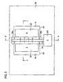
- a schematic plane pattern configuration of a semiconductor device according to a first embodiment of the present invention is expressed as shown in Fig. 3 .
- a schematic section structure taken in the line I - I of Fig. 3 is expressed as shown in Fig. 4
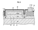
- a schematic section structure taken in the line II - II of Fig. 3 is expressed as shown in Fig. 5 .
- Al x Ga 1-x N aluminum gallium nitride layer
- the trench region 28a is formed including a part of the active area near the gate electrode 24, as shown in Fig. 5 .
- a gate terminal electrode 240 which is connected to the gate electrode 24 and is placed on the isolation region 34 may be further included, and the trench region 28b may be formed including a part of the active area AA between the gate electrode 24 and the gate terminal electrode 240.
- the isolation region 34 is formed of ion implantation.
- ion species nitrogen (N), argon (Ar), etc. are applicable, for example.
- the amount dosage accompanying the ion implantation is about 1x10 14 (ions/cm 2 ), for example, and accelerating energy is about 100 keV to about 200 keV.
- the insulating layer 30 for passivation is formed on the isolation region 34 and the device surface.
- this insulating layer 30 can form with a nitride film, an alumina (Al 2 O 3 ) film, an oxide film (SiO 2 ), an oxy-nitride film (SiON), etc. deposited by the PECVD (Plasma Enhanced Chemical Vapor Deposition) method, for example.
- the source electrode 20 and the drain electrode 22 are formed by aluminum (Al), Ti/Au, etc., for example.
- the gate electrode 24 can be formed, for example by Ni/Au etc.
- the source electrode contact 20a and the drain electrode contact 22a can be formed by the layered structure, which is composed of Al/Ti or Ni/Al/Ti, for example.
- the substrate 10 can be composed of a silicon carbide (SiC) substrate, a semi insulating silicon substrate, a sapphire substrate, etc.
- the nitride based compound semiconductor layer 12 is formed, for example by a GaN layer.
- the comparison result of an amount of variations of a normalized current ratio I dss /I dss0 of the semiconductor device according to the first embodiment and the semiconductor device according to the conventional example is shown in Fig. 6 by applying a horizontal axis into time t (hours).
- the amount of variations of the normalized current ratio I dss /I dss0 expresses the ratio of the saturation current value I dss between the drain and the source for saturation current value I dss0 of an initial state.
- the conventional example as for a comparison corresponds to the perfect planar structure which forms the isolation region 34 by ion implantation as well as the semiconductor device according to the first embodiment, and does not form the trench regions 28a and 28b.
- the trench regions 28a and 28b are formed including a part of the active area AA near the gate electrode 24, in the tip region of the gate electrode 24.
- the step of being connected to the gate electrode 24 and forming the gate terminal electrode 240 on the isolation region 34 may be further included, and the trench region 28b may form including a part of the active area AA between the gate electrode 24 and the gate terminal electrode 240.
- the isolation region 34 is formed by ion implantation.
- step (a) to step (h) the semiconductor device according to the first embodiment is completed.
- the semiconductor device in the semiconductor device composed of the GaN layer 12, the AlGaN layer 14, etc. in which isolation is performed by ion implanted processing, the semiconductor device in which it is high reliable and a miniaturization is realizable, and the fabrication method for the same can be provided by etching the part under the gate electrode 24 and forming the trench regions 28a and 28b.
- the first embodiment by etching the part under the gate electrode 24 and forming the trench regions 28a and 28b, an electron can be prevented from being injected into GaN layer 12, accordingly, the current collapse phenomenon in which the drain current of the device decreases gradually can be suppressed, and the semiconductor device in which it is high reliable and a miniaturization is realizable, and a fabrication method for the same can be provided.
- the semiconductor device in which the miniaturization of the gate electrode is realizable and whose high frequency characteristics also improve, and a fabrication method for the same can be provided.
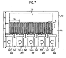
- FIG. 7 An overall schematic plane pattern configuration of a semiconductor device according to a second embodiment is expressed as shown in Fig. 7 . Moreover, the enlarged drawing of the part A of Fig. 7 is expressed as shown in Fig. 8 . Since the fundamental element section structure is the same as that of Fig. 4 to Fig. 5 shown in the first embodiment, the description of each layer is omitted.
- an electrode pattern assignment for high power and the trench region 38a formed under the gate electrode 24 are provided.
- the trench region 38a is formed including a part of the active area AA near the gate electrode 24.
- the trench region may be formed including a part of the active area AA between the gate electrode 24 and the gate terminal electrode 240 as well as the configuration of the trench region 38b shown in Fig. 3 .
- the isolation region 34 is formed by ion implantation.
- the cell width W 1 is about 120 micrometers
- W 2 is about 80 micrometers
- the cell length W 3 is about 100 micrometers
- W 4 is about 120 micrometers
- a VIA hole 260 is formed from the backside of the substrate 10, and the ground conductor is formed on the backside of the substrate 10. And when grounding a circuit element, the circuit element provided on the substrate 10 and the ground conductor formed on the backside of the substrate 10 are electrically connected via the VIA hole 260 which passes through the substrate 10.
- the gate terminal electrode 240 is connected to a surrounding semiconductor chip by a bonding wire etc.
- the drain terminal electrode 220 is also connected to a surrounding semiconductor chip by a bonding wire etc.
- the trench region 38 are formed including a part of the active area AA near the gate electrode 24 having a plurality of fingers, in the tip region of the gate electrode 24.
- the isolation region 34 is formed by ion implantation.
- a schematic plane pattern configuration of a semiconductor device according to a modified example of the second embodiment is expressed as shown in Fig. 9 .
- the trench region 38a is formed in stripe shape in parallel to the arrangement direction of a plurality of finger electrodes including a part of the active area AA near the gate electrode 24.
- the trench region 38a is formed in stripe shape in parallel to the arrangement direction of a plurality of finger electrodes including a part of the active area AA near the gate electrode 24.
- the trench region 38b may be formed under the gate electrode 24 having a plurality of fingers including a part of the active area AA between the gate terminal electrode 240 placed on the isolation region 34 and the gate electrode 24 having a plurality of fingers.
- these trench regions 38b may be formed in stripe shape in parallel to the arrangement direction of a plurality of finger electrodes as well as Fig. 9 .
- the semiconductor device for high power which is composed of the GaN layer 12, the AlGaN layer 14, etc. in which isolation is performed by ion implantation processing
- the semiconductor device for high power in which it is highly reliable and a miniaturization is realizable, and the fabrication method for the same can be provided by etching the part under the gate electrode 24 and forming the trench region 38a.
- the second embodiment of the present invention by etching the part under the gate electrode 24 and forming the trench region 38a, an electron can be prevented from being injected into GaN layer 12, accordingly, the current collapse phenomenon in which the drain current of the device decreases gradually can be suppressed, and the semiconductor device for high power in which it is highly reliable and a miniaturization is realizable, and a fabrication method for the same can be provided.
- the semiconductor device for high power in which the miniaturization of the gate electrode 24 is realizable and whose high frequency characteristics also improve, and a fabrication method for the same can be provided.
- the schematic plane pattern configuration of a semiconductor device according to a third embodiment of the present invention is expressed as shown in Fig. 10 .
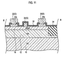
- the schematic section structure taken in the line III - III of Fig. 10 is expressed as shown in Fig. 11 or Fig. 12 .
- the example of Fig. 11 is a section structure which forms an isolation region 34 acting as a non-active area NA by using ion implantation technology
- the example of Fig. 12 is a section structure which forms an isolation region 25 acting as a non-active area NA by using mesa etching technology.
- Al x Ga 1-x N aluminum gallium nitride layer
- the isolation region 34 is formed of ion implantation.
- ion species nitrogen (N), argon (Ar), etc, are applicable, for example.
- the amount of dosage accompanying the ion implantation is about 1 ⁇ 10 14 (ions/cm 2 ), for example, and accelerating energy is about 100 keV to about 200 keV.
- An insulating layer 30 for passivation is formed on the isolation region 34 and the device surface.
- this insulating layer 30 can form with a nitride film, an alumina (Al 2 O 3 ) film, an oxide film (SiO 2 ), an oxy-nitride film (SiON), etc. deposited by the PECVD (Plasma Enhanced Chemical Vapor Deposition) method, for example.
- the insulating layer 30 for passivation may be placed also in the trench region 28.
- the source electrode 20 and the drain electrode 22 are formed by aluminum (Al), Ti/Au, etc., for example.
- the gate electrode 24 can be formed of Ni/Au etc, for example.
- the source electrode contact 20a and the drain electrode contact 22a can be formed by the layered structure, which is composed of Al/Ti or Ni/Al/Ti, for example.
- the substrate 10 may be provided with either of an SiC substrate, a GaN substrate, a substrates in which the GaN epitaxial layer is formed on the SiC substrate, a substrate in which the GaN epitaxial layer is formed on the Si substrate, a substrate in which the hetero-junction epitaxial layer composed of GaN/AlGaN is formed on the SiC substrate, a substrate in which the GaN epitaxial layer is formed on the sapphire substrate, and a sapphire substrate or a diamond substrate.
- the nitride based compound semiconductor layer 12 is formed, for example by a GaN layer.
- the trench region 28 is formed including a part of the active area AA, for example, as shown in Fig. 13 . Moreover, the trench region 28 is formed including a part of the isolation region 34 between the gate electrode 24 and the drain terminal electrode 220, as shown in Fig. 13 . Moreover, as shown in Fig. 13 , in the trench region 28, the tip region of the gate electrode 24 extends and is placed.
- the sidewall of the trench region 28 is provided with stepping structure, for example, as shown in Fig. 14 .
- Two or more steps of numbers of steps may be formed not only in two steps.
- the stepping structure may be provided in the sidewall part by the side of the semiconductor.
- a plurality of trench regions may be formed, for example, as shown in Fig. 15 .
- three trench regions 28a, 28b, and 28c are formed.
- the trench regions 28a, 28b, and 28c are formed including a part of the isolation region 34 between the gate electrode 24 and the drain terminal electrode 220, as shown in Fig. 15 . It fills up with the insulating layer 30 in the trench region 28a and 28b.
- the tip region of the gate electrode 24 it is formed in the trench region 28c including a part of active area AA.
- the tip region of the gate electrode 24 extends and is placed in the trench region 28c.
- the tip region and the drain terminal electrode 220 of the gate electrode 24 may be provided with the isolated structure by the trench region 28.
- the insulating layer 30 is formed in the trench region 28.
- Fig. 10 two trench regions 28 of each other shown in Fig. 10 are combined, and the arrangement direction of the source electrode 20, the gate electrode 24, and the drain electrode 22 may be provided with stripe geometry.
- trench region where structure is substantially equal to the trench region 28 may be formed between the gate electrode 24 and the gate terminal electrode 240.
- the tip region of the stripe of the gate electrode 24 although it is easy to concentrate an electric field also in a terminal part, it is because generating of the leakage current between the gate and the drain can be suppressed by forming another trench region.
- the step of forming the trench region 28 is preferable to perform after the step of forming the isolation regions (34, 25).
- ion implantation technology can be used for the step of forming the isolation region 34.
- mesa etching can be used for the step of forming the isolation region 25.
- the structure of the trench region 28 can apply the structure shown in Fig. 13 to Fig. 16 , for example.
- step (a) to step (i) the semiconductor device according to the third embodiment is completed.
- the leakage current between gate drains can be decreased, and a highly reliable and high performance semiconductor device for high power and a fabrication method for the same can be provided.
- the surface leakage current between the gate and the drain can be decreased by lengthening distance between the gate electrode 24 and the drain terminal electrode 220 effectually, and a highly reliable and high performance semiconductor device for high power and a fabrication method for the same can be provided.
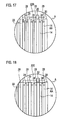
- FIG. 17 The schematic plane pattern configuration of a semiconductor device according to a fourth embodiment is expressed as well as shown in Fig. 7 . Moreover, in the semiconductor device according to the fourth embodiment, the enlarged drawing of the part A of Fig. 7 is expressed as shown in Fig. 17 .
- the semiconductor device according to the fourth embodiment shown in Fig. 7 and Fig. 17 it has the electrode pattern assignment for large amount of power, and the trench region 28 formed between the gate electrode 24 and the drain terminal electrode 220.
- Al x Ga 1-x N aluminum gallium nitride layer
- the isolation region 34 is formed of ion implantation technology, for example.
- the trench region 28 may be formed including a part of the active area AA.
- the trench region 28 may be formed including a part of isolation region 34 between the gate electrode 24 and the drain terminal electrode 220 which have a plurality of fingers.
- the tip region of the gate electrode 24, which has a plurality of fingers may be extended and placed.
- the sidewall of the trench region 28 may be provided with stepping structure as well as the structure shown in Fig. 14 .
- a plurality of trench regions 28 may be formed as well as the structure shown in Fig. 15 .
- the tip region of the gate electrode 24, which have a plurality of fingers, and the drain terminal electrode 220 may be isolated by the trench region 28, and the insulating layer 30 for passivation may be formed in the trench region 28.
- trench region where structure is substantially equal to the trench region 28 may be formed between the gate electrode 24, which have a plurality of fingers, and the gate terminal electrode 240.
- the tip region of the stripe of the gate electrode 24 although it is easy to concentrate an electric field also in a terminal part, it is because generating of the leakage current between the gate and the drain can be suppressed by forming another trench region.
- the substrate 10 may be provided with either of an SiC substrate, a GaAs substrate, a GaN substrate, a substrates in which the GaN epitaxial layer is formed on the SiC substrate, a substrate in which the GaN epitaxial layer is formed on the Si substrate, a substrate in which the hetero-junction epitaxial layer composed of GaN/AlGaN is formed on the SiC substrate, a substrate in which the GaN epitaxial layer is formed on the sapphire substrate, and a sapphire substrate or a diamond substrate.
- the cell width W 1 is about 120 micrometers
- W 2 is about 80 micrometers
- the cell length W 3 is about 100 micrometers
- W 4 is about 120 micrometers
- a VIA hole 260 is formed from the backside of the substrate 10, and the ground conductor is formed on the backside of the substrate 10. And when grounding a circuit element, the circuit element provided on the substrate 10 and the ground conductor formed on the backside of the substrate 10 are electrically connected via the VIA hole 260 which passes through the substrate 10.
- the gate terminal electrode 240 is connected to a surrounding semiconductor chip by a bonding wire etc.
- the drain terminal electrode 220 is also connected to a surrounding semiconductor chip by a bonding wire etc.
- the step of forming the trench region 28 is preferable to perform after the step of forming the isolation regions (34, 25).
- the ion implantation technology can be used for the step of forming the isolation region 34.
- the mesa etching technology can be used for the step of forming the isolation region 25.
- a schematic plane pattern configuration of a semiconductor device according to a modified example of the fourth embodiment is expressed as shown in Fig. 18 .
- the trench region 28 has the characteristic at the point provided with stripe geometry in parallel to the arrangement direction of a plurality of finger electrodes between the gate electrode 24 which have a plurality of fingers and the drain terminal electrode 220.
- trench region where structure is substantially equal to the trench region 28 may be formed between the gate electrode 24 which have a plurality of fingers and the gate terminal electrode 240.
- the tip region of the stripe of the gate electrode 24 although it is easy to concentrate an electric field also in a terminal part, it is because generating of the leakage current between the gate and the drain can be suppressed by forming another trench region.
- the leakage current between the gate and the drain can be decreased, and a highly reliable and high performance semiconductor device for high power and a fabrication method for the same can be provided.
- the surface leakage current between the gate and the drain can be decreased by lengthening distance between the gate electrode 24 and the drain terminal electrode 220 effectively, and a highly reliable and high performance semiconductor device for high power and a fabrication method for the same can be provided.
- the semiconductor devices according to the embodiment of the present invention are applicable not only to FETs but also other amplifying elements, such as HEMTs (High Electron Mobility Transistors), LDMOS (Lateral Doped Metal-Oxide-Semiconductor) FETS, HBTs (Hetero-junction Bipolar Transistors), and MEMS (Micro Electro Mechanical Systems) devices.
- HEMTs High Electron Mobility Transistors
- LDMOS Layer Doped Metal-Oxide-Semiconductor
- HBTs Hetero-junction Bipolar Transistors
- MEMS Micro Electro Mechanical Systems
- a semiconductor device has a wide range of application fields, such as an internally matched power amplifier, a power MMIC (Monolithic Microwave Integrated Circuit), a microwave power amplifier, a millimeter wave power amplifier, and a high frequency MEMS device.
- a power MMIC Monolithic Microwave Integrated Circuit
Landscapes
- Junction Field-Effect Transistors (AREA)
Abstract
Description
- The present invention relates to a semiconductor device and a fabrication method for the same. In particular, the present invention relates to a semiconductor device for highly reliable and high power, which composes gallium nitride (GaN) etc., and a fabrication method for the same.
- It is known that an FET (Field Effect Transistor) using a gallium nitride (GaN) based semiconductor has large current collapse and large leakage current. The crystal dislocation and crystal defect, which are one of the causes in an epitaxial crystal are mentioned.
- Since the crystal defects degrades fundamental performances of the GaN based FETs, such as increase of leakage current, and generating of a current collapse phenomenon, it is dramatically important to obtain an epitaxial layer with little crystal defects.
- In order to decrease the crystal dislocation and the crystal defect of a GaN epitaxial layer, inserting an aluminum gallium nitride (AlGaN) layer and an aluminum nitride (AlN) layer into a GaN layer is known.
- As shown in
Fig. 1 , the configuration of the basic unit of the conventional high power semiconductor device, which is composed of a gallium nitride layer, an aluminum gallium nitride (AlGaN) layer, etc. includes aGaN layer 12 placed on thesubstrate 10 which is composed of SiC; anAlGaN layer 14 placed on theGaN layer 12; and agate electrode 24, asource electrode 20, and adrain electrode 22 which are placed on theAlGaN layer 14. - Furthermore, as shown in
Fig. 1 . as for the conventional semiconductor device, the isolation region acting as a non-active area NA is formed in the periphery of an active area AA which is composed of the AlGaNlayer 14, by using mesa etching technology, ion implantation technology, etc. - As shown in
Fig. 1 , thegate electrode 24, thesource electrode 20, and thedrain electrode 22 are connected to agate terminal electrode 240, asource terminal electrode 200, and adrain terminal electrode 220 which are placed on the isolation region acting as the non-active area NA, respectively. -
Fig. 2 shows a schematic section structure taken in the line I - I ofFig. 1 , and is an example in which anisolation region 25 which acts as the non-active area NA in the periphery of the active area AA by mesa etching technology is formed. Asource electrode contact 20a is placed between thesource electrode 20 and theAlGaN layer 14, and adrain electrode contact 22a is placed between thedrain electrode 22 and theAlGaN layer 14. - That is, as shown in
Fig. 2 , theisolation region 25 is formed by mesa etching of a part of the AlGaNlayer 14 and theGaN layer 12 in the periphery of the AA area of the conventional semiconductor device. The active area AA of the semiconductor device is specified by theisolation region 25 formed by mesa etching. In addition, aninsulating layer 30 acting as a passivation film is formed on the sidewall part of theisolation region 25 formed by mesa etching and the active area, as shown inFig. 2 . - As shown in
Fig. 1 , the conventional semiconductor device is electrically insulated between the gate and the drain by the isolation region acting as the non-active area NA except for the active area AA. For this reason, originally, an amount of surface leakage current does not flow between the gate and the drain on the isolation regions except for the active area AA. - However, when a great value of voltage is applied between the gate and drain, an electric field concentrates on the gate electrode tip region GP between the
gate electrode 24 and thedrain terminal electrode 220. For this reason, an amount of surface leakage current flows between thegate electrode 24 and thedrain terminal electrode 220, and the characteristic degradation of a semiconductor device is caused. There is a problem of resulting in the breakdown of a semiconductor device depending on the case. - For example, since GaN and AlGaN or AlN have large lattice constant difference, and electric charges induced by piezoelectric polarization effect are generated between a
GaN layer 12 and anAlGaN layer 14, there is problem that the electric charges generated in theGaN layer 12 will degrade a high frequency performance of a semiconductor device extremely. - The electric charges induced by such piezoelectric polarization effect becomes the cause of increasing the conductivity of the
GaN layer 12, increasing leakage current between agate electrode 24 and asource electrode 20 or between agate electrode 24 and adrain electrode 22, and reducing the power amplification gain of a semiconductor device. - A field effect transistor using the GaN based semiconductor which can form a gate size in 0.1 micrometer class, and is not occurred leakage current between a gate electrode and a source electrode or a drain electrode, and a fabrication method for the same, are already disclosed (for example, refer to Patent Literature 1). In the
Patent Literature 1, the gate leakage current is reduced by using the field effect transistor having a gate electrode in which the sectional shape is T shape. - Moreover, a high resistivity group III nitride semiconductor crystal, the group III nitride semiconductor substrate, and the semiconductor device , and a fabrication method of the group III nitride semiconductor crystal, are already disclosed (for example, refer to Patent Literature 2). In the Patent Literature 2, the Fe doped GaN layer, which is the group III nitride semiconductor crystal in which Fe is doped as transition metals, for example, and whose Ga atom vacancy density is not more than 1×1016 cm-3 is disclosed. The Fe atoms density of the Fe doped GaN layer is 5×1017 cm-3 to 5×1020 cm-3. Moreover, a semiconductor device which has the semiconductor layer formed on the group III nitride semiconductor substrate which is composed of the above-mentioned Fe doped GaN layer is also disclosed.
- Moreover, it is already disclosed also about a semiconductor element which can perform multilayer formation of a plurality of nitride based compound semiconductor layers which have a difference of the lattice constant more than a predetermined value in the effective crystalline state, and can suppress propagation of the threading dislocations to an epitaxial growth direction (for example, refer to Patent Literature 3).
- In the high power semiconductor device which is composed of a GaN layer, an AlGaN layer, etc., when electrical isolation is performed by the ion implantation (implanted isolation) technology, there is a problem that the reliability of the power semiconductor device decreases to a low value.
- On the other hand, in the high power semiconductor device which is composed a GaN layer, an AlGaN layer, etc., since a step is made to a device in the electrical isolation method by mesa etching, there is a problem that a focus becomes difficult to match when forming wiring etc. with an exposure device, and it becomes difficult to perform a miniaturization.
-
- Patent Literature 1: Japanese Patent Application Laying-Open Publication No.
2002-141499 - Patent Literature 2: Japanese Patent Application Laying-Open Publication No.
2007-184379 - Patent Literature 3: Japanese Patent Application Laying-Open Publication No.
2007-221001 - The purpose of the invention is to provide a semiconductor device in which it is high reliable, high performance, and high power and a fabrication method for the same.
- According to an aspect of the invention, a nitride based semiconductor device comprises a substrate; a nitride based compound semiconductor layer placed on the substrate; an active area which is placed on the nitride based compound semiconductor layer, and is composed of an aluminum gallium nitride layer (AlxGa1-xN) (where 0.1<=x<=1); an isolation region which performs isolation of the active area mutually; a trench region formed by etching for a part of previous arrangement to a gate electrode; and a gate electrode, a source electrode, and a drain electrode which are placed on the active area surrounded by the isolation region, wherein the trench region is formed including a part of the active area near the gate electrode, in the tip region of said gate electrode.
- According to another aspect of the invention, a nitride based semiconductor device comprises a substrate; a nitride based compound semiconductor layer placed on the substrate; an active area which is placed on the nitride based compound semiconductor layer, and is composed of an aluminum gallium nitride layer (AlxGa1-xN) (where 0.1<=x<=1); an isolation region which performs isolation of the active area mutually; a gate electrode, a source electrode, and a drain electrode which have been placed on the active area surrounded by the isolation region; a gate terminal electrode, a source terminal electrode, and a drain terminal electrode which is placed on the isolation region and is connected to the gate electrode, the source electrode, and the drain electrode, respectively; and a trench region formed between the gate electrode and the drain terminal electrode.
- According to another aspect of the invention, a fabrication method for a nitride based semiconductor device comprises forming a nitride based compound semiconductor layer on a substrate; forming an active area composed of an aluminum gallium nitride layer (AlxGa1-xN) (where 0.1<=x<=1) on the nitride based compound semiconductor layer; forming an isolation region which performs isolation of the active area mutually; etching a part of previous arrangement part of a gate electrode, and forming a trench region; and forming a gate electrode, a source electrode, and a drain electrode on the active area surrounded by the isolation region, wherein in the step of forming the trench region, the trench region is formed including the a part of active area near the gate electrode, in the tip region of the gate electrode.
- According to another aspect of the invention, a fabrication method for a nitride based semiconductor device comprises forming a nitride based compound semiconductor layer on a substrate; forming an active area composed of an aluminum gallium nitride layer (AlxGa1-xN) (where 0.1<=x<=1) on the nitride based compound semiconductor layer; forming an isolation region which performs isolation of the active area mutually; etching a part of previous arrangement part of a gate electrode having a plurality of fingers, and forming a trench region; forming a gate electrode, a source electrode, and a drain electrode which have a plurality of fingers, respectively on a first surface of the active area surrounded by the isolation region; and forming a gate terminal electrode, a source terminal electrode, and a drain terminal electrode which govern a plurality of fingers, respectively and are formed on the first surface of the substrate for every the gate electrode, the source electrode, and the drain electrode.
- According to another aspect of the invention, a fabrication method for a nitride based semiconductor device comprises forming a nitride based compound semiconductor layer on a substrate; forming an active area which is composed of an aluminum gallium nitride layer (AlxGa1-xN) (where 0.1<=x<=1) on the nitride based compound semiconductor layer; forming an isolation region which performs isolation of the active area mutually; forming a gate electrode, a source electrode, and a drain electrode on the active area surrounded by the isolation region; forming a gate terminal electrode, a source terminal electrode, and a drain terminal electrode which are connected to the gate electrode, the source electrode, and the drain electrode, respectively on the isolation region; and forming a trench region between the gate electrode and the drain terminal electrode.
- According to the present invention, the semiconductor device for high reliable, high performance and high power and the fabrication method for the same can be provided.
-
-
Fig. 1 is a schematic plane pattern configuration diagram of a semiconductor device according to a conventional example. -
Fig. 2 is a schematic cross-sectional configuration chart taken in the line I - I ofFig. 1 . -
Fig. 3 is a schematic plane pattern configuration diagram of a semiconductor device according to a first embodiment of the present invention. -
Fig. 4 shows the semiconductor device according to the first embodiment of the present invention, and is a schematic cross-sectional configuration chart taken in the line I - I ofFig. 3 . -
Fig. 5 shows the semiconductor device according to the first embodiment of the present invention, and is a schematic cross-sectional configuration chart taken in the line II - II ofFig. 3 . -
Fig. 6 shows a comparison result of the amount of variations of normalized current ratio Idss/Idss0, which applies time t for the horizontal axis, of the semiconductor device according to the first embodiment of the present invention, and the semiconductor device according to the conventional example. -
Fig. 7 is an overall schematic plane pattern configuration diagram of a semiconductor device according to a second embodiment of the present invention. -
Fig. 8 is an enlarged drawing of part A ofFig. 7 . -
Fig. 9 is a schematic plane pattern configuration diagram of a semiconductor device according to the modified example of the second embodiment of the present invention. -
Fig. 10 is a schematic plane pattern configuration diagram of a semiconductor device according to a third embodiment of the present invention. -
Fig. 11 is a schematic cross-sectional configuration chart, which forms an isolation region by ion implantation and is taken in the line III - III ofFig. 10 . -
Fig. 12 is a schematic cross-sectional configuration chart, which forms an isolation region by mesa etching and is taken in the line III - III ofFig. 10 . -
Fig. 13 shows an example 1 of schematic section structure taken in the line IV - IV ofFig. 10 . -
Fig. 14 shows an example 2 of schematic section structure taken in the line IV - IV ofFig. 10 . -
Fig. 15 shows an example 3 of schematic section structure taken in the line IV - IV ofFig. 10 . -
Fig. 16 shows an example 4 of schematic section structure taken in the line IV - IV ofFig. 10 . -
Fig. 17 is a schematic plane pattern configuration diagram of a semiconductor device according to a fourth embodiment of the present invention. -
Fig. 18 is a schematic plane pattern configuration diagram of a semiconductor device according to a modified example of the fourth embodiment of the present invention. - There will be described embodiments of the present invention, with reference to the drawings, where like members or elements are designated by like reference characters to eliminate redundancy, and some layers and their subsidiary regions are designated by the same reference characters for simplicity. Drawings are schematic, not actual, and may be inconsistent in between in scale, ratio, etc.
- The embodiments to be described are embodiments of a technical concept or spirit of the present invention that is not limited to embodied specifics, and may be changed without departing from the spirit or scope of claims.
- A schematic plane pattern configuration of a semiconductor device according to a first embodiment of the present invention is expressed as shown in
Fig. 3 . Moreover, a schematic section structure taken in the line I - I ofFig. 3 is expressed as shown inFig. 4 , and a schematic section structure taken in the line II - II ofFig. 3 is expressed as shown inFig. 5 . - As shown in
Fig. 3 to Fig. 5 , the semiconductor device according to the first embodiment includes asubstrate 10; a nitride basedcompound semiconductor layer 12 placed on thesubstrate 10; an active area AA which is placed on the nitride basedcompound semiconductor layer 12, and is composed of the aluminum gallium nitride layer (AlxGa1-xN) (where 0.1<=x<=1) 14; anisolation region 34 which performs isolation of the active area AA mutually; atrench region 28a formed by etching for a part of previous arrangement to thegate electrode 24; and agate electrode 24, asource electrode 20, and adrain electrode 22 which are placed on the active area AA surrounded by theisolation region 34. - The
isolation region 34 is formed to a part of depth direction of the aluminum gallium nitride layer (AlxGa1-xN) (where 0.1<=x<=1) 14 and the nitride basedcompound semiconductor layer 12. - In the tip region of the
gate electrode 24, thetrench region 28a is formed including a part of the active area near thegate electrode 24, as shown inFig. 5 . - Furthermore, as shown in
Fig. 3 andFig. 5 , agate terminal electrode 240 which is connected to thegate electrode 24 and is placed on theisolation region 34 may be further included, and thetrench region 28b may be formed including a part of the active area AA between thegate electrode 24 and thegate terminal electrode 240. - The
isolation region 34 is formed of ion implantation. As ion species, nitrogen (N), argon (Ar), etc. are applicable, for example. Moreover, the amount dosage accompanying the ion implantation is about 1x10¹⁴ (ions/cm2), for example, and accelerating energy is about 100 keV to about 200 keV. - The insulating
layer 30 for passivation is formed on theisolation region 34 and the device surface. As this insulatinglayer 30, it can form with a nitride film, an alumina (Al2O3) film, an oxide film (SiO2), an oxy-nitride film (SiON), etc. deposited by the PECVD (Plasma Enhanced Chemical Vapor Deposition) method, for example. - A
source electrode contact 20a is formed on the interface between thesource electrode 20 and the aluminum gallium nitride layer (AlxGa1-xN) (where 0.1<=x<=1) 14, and adrain electrode contact 22a is formed on the interface between thedrain electrode 22 and the aluminum gallium nitride layer (AlxGa1-xN) (where 0.1<=x<=1) 14. Thesource electrode 20 and thedrain electrode 22 are formed by aluminum (Al), Ti/Au, etc., for example. - The
gate electrode 24 can be formed, for example by Ni/Au etc. - The
source electrode contact 20a and thedrain electrode contact 22a can be formed by the layered structure, which is composed of Al/Ti or Ni/Al/Ti, for example. - A two-dimensional electron gas layer is formed on the interface between the nitride based
compound semiconductor layer 12 and the aluminum gallium nitride layer (AlxGa1-xN) (where 0.1<=x<=1) 14 placed on the nitride basedcompound semiconductor layer 12. - The
substrate 10 can be composed of a silicon carbide (SiC) substrate, a semi insulating silicon substrate, a sapphire substrate, etc. - The nitride based
compound semiconductor layer 12 is formed, for example by a GaN layer. - The comparison result of an amount of variations of a normalized current ratio Idss/Idss0 of the semiconductor device according to the first embodiment and the semiconductor device according to the conventional example is shown in
Fig. 6 by applying a horizontal axis into time t (hours). InFig. 6 , the amount of variations of the normalized current ratio Idss/Idss0 expresses the ratio of the saturation current value Idss between the drain and the source for saturation current value Idss0 of an initial state. In this case, the conventional example as for a comparison corresponds to the perfect planar structure which forms theisolation region 34 by ion implantation as well as the semiconductor device according to the first embodiment, and does not form thetrench regions - As clearly from
Fig. 6 , in the conventional example, the variation per hour of the amount of normalized current ratio Idss/Idss0 is remarkable, and the saturation current value between the drain and the source decreases with the passage of time. On the other hand, in the semiconductor device according to the first embodiment, reduction of the saturation current value is suppressed by etching the part under thegate electrode 24 and forming thetrench regions - A fabrication method of the semiconductor device according to the first embodiment includes the step of forming the nitride based
compound semiconductor layer 12 on thesubstrate 10; the step of forming the active area AA which is composed of the aluminum gallium nitride layer (AlxGa1-xN) (where 0.1<=x<=1) 14 on the nitride basedcompound semiconductor layer 12; the step of forming theisolation region 34 which performs isolation of the active area AA mutually; the step of etching a part of previous arrangement part of thegate electrode 24, and forming thetrench regions gate electrode 24, thesource electrode 20, and thedrain electrode 22 on the active area AA surrounded by theisolation region 34. - In the step of forming the
isolation region 34, theisolation region 34 is formed to a part of depth direction of the aluminum gallium nitride layer (AlxGa1-xN) (where 0.1<=x<=1) 14 and the nitride basedcompound semiconductor layer 12. - In the step of forming the
trench regions trench regions gate electrode 24, in the tip region of thegate electrode 24. - The step of being connected to the
gate electrode 24 and forming thegate terminal electrode 240 on theisolation region 34 may be further included, and thetrench region 28b may form including a part of the active area AA between thegate electrode 24 and thegate terminal electrode 240. - In the step of forming the
isolation region 34, theisolation region 34 is formed by ion implantation. - In the following, the fabrication method of the semiconductor device according to the first embodiment of the present invention will be explained.
- (a) Pouring TMG (trimethyl gallium) and ammonia gas on the
SiC substrate 10, and formingGaN layer 12 in a thickness of about 1 micrometer to about 2 micrometers, for example, with epitaxial growth. - (b) Next, pouring TMA1 (trimethyl aluminum) and ammonia gas, and forming the aluminum gallium nitride layer (Al0.3Ga0.7N) 14 of about 30% of an Aluminum composition ratio in a thickness of about 20 nm to about 100 nm with epitaxial growth, for example.
- (c) Next, forming the
isolation region 34 which performs isolation of the active area AA mutually by ion implantation technology. As ion species, nitrogen (N), argon (Ar), etc. are applicable, for example. Moreover, the amount of dosage accompanying the ion implantation is about 1×10¹⁴ (ions/cm2), for example, and accelerating energy is about 100 keV to about 200 keV. - (d) Next, etching a part of previous arrangement part of the
gate electrode 24 by dry etching technology, and forming thetrench regions trench regions trench regions - (e) Next, forming the
source electrode contact 20a and thedrain electrode contact 22a on the active area AA surrounded by theisolation region 34. As the electric contact formation technology, vacuum deposition technology, sputtering technology, etc. are applicable. Thesource electrode contact 20a and thedrain electrode contact 22a are formed as an ohmic electrode by the layered structure which is composed of Al/Ti or Ni/Al/Ti, for example. - (f) Next, forming the
gate electrode 24. As the electrode formation technology, vacuum deposition technology, sputtering technology, etc. are applicable. Thegate electrode 24 can be formed by Ni/Au etc., for example. Thegate electrode 24 forms Schottky contact between the aluminum gallium nitride layer (AlxGa1-xN) (where 0.1<=x<=1) 14 and thegate electrode 24. The width of thegate electrode 24 is about 0.1 micrometer to about 1 micrometer, for example. - (g) Next, forming the insulating
layer 30 for passivation on the whole device surface. This insulatinglayer 30 can be formed with a nitride film, an Al2O3 film, an SiO2 film, an SiON film, etc. deposited by the PECVD method, for example. - (h) Next, forming the
source electrode 20 and thedrain electrode 22. As the electrode formation technology, vacuum deposition technology, sputtering technology, etc. are applicable. Thesource electrode 20 and thedrain electrode 22 are formed by aluminum (Al), Ti/Au, etc., for example. - According to the above-mentioned step (a) to step (h), the semiconductor device according to the first embodiment is completed.
- According to the first embodiment, in the semiconductor device composed of the
GaN layer 12, theAlGaN layer 14, etc. in which isolation is performed by ion implanted processing, the semiconductor device in which it is high reliable and a miniaturization is realizable, and the fabrication method for the same can be provided by etching the part under thegate electrode 24 and forming thetrench regions - According to the first embodiment, by etching the part under the
gate electrode 24 and forming thetrench regions GaN layer 12, accordingly, the current collapse phenomenon in which the drain current of the device decreases gradually can be suppressed, and the semiconductor device in which it is high reliable and a miniaturization is realizable, and a fabrication method for the same can be provided. - According to the first embodiment, by unevenness on the surface of the device almost being exhausted, focusing of an exposure device becomes easy and, accordingly, the semiconductor device in which the miniaturization of the gate electrode is realizable and whose high frequency characteristics also improve, and a fabrication method for the same can be provided.
- An overall schematic plane pattern configuration of a semiconductor device according to a second embodiment is expressed as shown in
Fig. 7 . Moreover, the enlarged drawing of the part A ofFig. 7 is expressed as shown inFig. 8 . Since the fundamental element section structure is the same as that ofFig. 4 to Fig. 5 shown in the first embodiment, the description of each layer is omitted. - In the semiconductor device according to the second embodiment, an electrode pattern assignment for high power and the
trench region 38a formed under thegate electrode 24 are provided. - As shown in
Fig. 4 to Fig. 5 andFig. 7 to Fig. 8 , the overall configuration of the semiconductor device according to the second embodiment includes asubstrate 10; a nitride basedcompound semiconductor layer 12 placed on thesubstrate 10; an active area AA which is placed on the nitride basedcompound semiconductor layer 12, and is composed of the aluminum gallium nitride layer (AlxGa1-xN) (where 0.1<=x<=1) 14; anisolation region 34 which performs isolation of the active area AA mutually; atrench region 38a formed by etching for a part of previous arrangement to thegate electrode 24 having a plurality of fingers; agate electrode 24, asource electrode 20, and adrain electrode 22 which are placed on a first surface of the active area AA surrounded by theisolation region 34, and have a plurality of fingers, respectively; agate terminal electrode 240, asource terminal electrode 200, and adrain terminal electrode 220 which are placed on a first surface of thesubstrate 10, govern a plurality of fingers, respectively and is formed for every thegate electrode 24, thesource electrode 20, and thedrain electrode 22. - The
isolation region 34 is formed to a part of depth direction of the aluminum gallium nitride layer (AlxGa1-xN) (where 0.1<=x<=1) 14 and the nitride basedcompound semiconductor layer 12. - In the tip region of the
gate electrode 24 having a plurality of fingers, thetrench region 38a is formed including a part of the active area AA near thegate electrode 24. - The trench region may be formed including a part of the active area AA between the
gate electrode 24 and thegate terminal electrode 240 as well as the configuration of thetrench region 38b shown inFig. 3 . - Moreover, the
isolation region 34 is formed by ion implantation. - In the configuration example of
Fig. 7 , as for the size of each part, for example, the cell width W1 is about 120 micrometers, W2 is about 80 micrometers, the cell length W3 is about 100 micrometers, W4 is about 120 micrometers, and the gate width WG is about 100 micrometer x 6 x 4 cell = 2.4 mm as a whole. - In the example of
Fig. 7 , in thesource terminal electrode 200, aVIA hole 260 is formed from the backside of thesubstrate 10, and the ground conductor is formed on the backside of thesubstrate 10. And when grounding a circuit element, the circuit element provided on thesubstrate 10 and the ground conductor formed on the backside of thesubstrate 10 are electrically connected via theVIA hole 260 which passes through thesubstrate 10. - In addition, the
gate terminal electrode 240 is connected to a surrounding semiconductor chip by a bonding wire etc., and thedrain terminal electrode 220 is also connected to a surrounding semiconductor chip by a bonding wire etc. - A fabrication method of the semiconductor device according to the second embodiment includes the step of forming the nitride based
compound semiconductor layer 12 on thesubstrate 10; the step of forming the active area AA which is composed of the aluminum gallium nitride layer (AlxGa1-xN) (where 0.1<=x<=1) 14 on the nitride basedcompound semiconductor layer 12; the step of forming theisolation region 34 which performs isolation of the active area AA mutually; the step of etching a part of previous arrangement part of thegate electrode 24 having a plurality of fingers, and forming thetrench region 38a; the step of forming thegate electrode 24, thesource electrode 20, and thedrain electrode 22 which have a plurality of fingers, respectively, on the first surface of the active area AA surrounded by theisolation region 34; and the step of forming thegate terminal electrode 240, thesource terminal electrode 200, and thedrain terminal electrode 220 which govern a plurality of fingers, respectively and are formed on the first surface of thesubstrate 10 every thegate electrode 24, thesource electrode 20, and thedrain electrode 22. - In the step of forming the
isolation region 34, theisolation region 34 is formed to a part of depth direction of the aluminum gallium nitride layer (AlxGa1-xN) (where 0.1<=x<=1) 14 and the nitride basedcompound semiconductor layer 12. - In the step of forming the trench region 38, the trench region 38 are formed including a part of the active area AA near the
gate electrode 24 having a plurality of fingers, in the tip region of thegate electrode 24. - In the step of forming the
isolation region 34, theisolation region 34 is formed by ion implantation. - Since it is the same as that of the first embodiment about the details of the fabrication method of the semiconductor device according to the second embodiment, the description is omitted.
- A schematic plane pattern configuration of a semiconductor device according to a modified example of the second embodiment is expressed as shown in
Fig. 9 . - In the semiconductor device according to the modified example of the 2nd embodiment, as shown in
Fig. 9 , in the tip region of thegate electrode 24 having a plurality of fingers, thetrench region 38a is formed in stripe shape in parallel to the arrangement direction of a plurality of finger electrodes including a part of the active area AA near thegate electrode 24. - In the step of forming the
trench region 38a also in a fabrication method of the semiconductor device according to the modified example of the second embodiment, in the tip region of thegate electrode 24 having a plurality of fingers, thetrench region 38a is formed in stripe shape in parallel to the arrangement direction of a plurality of finger electrodes including a part of the active area AA near thegate electrode 24. - Furthermore, as shown in
Fig. 3 andFig. 5 , thetrench region 38b may be formed under thegate electrode 24 having a plurality of fingers including a part of the active area AA between thegate terminal electrode 240 placed on theisolation region 34 and thegate electrode 24 having a plurality of fingers. - Moreover, these
trench regions 38b may be formed in stripe shape in parallel to the arrangement direction of a plurality of finger electrodes as well asFig. 9 . - According to the second embodiment of the present invention, in the semiconductor device for high power which is composed of the
GaN layer 12, theAlGaN layer 14, etc. in which isolation is performed by ion implantation processing, the semiconductor device for high power in which it is highly reliable and a miniaturization is realizable, and the fabrication method for the same can be provided by etching the part under thegate electrode 24 and forming thetrench region 38a. - According to the second embodiment of the present invention, by etching the part under the
gate electrode 24 and forming thetrench region 38a, an electron can be prevented from being injected intoGaN layer 12, accordingly, the current collapse phenomenon in which the drain current of the device decreases gradually can be suppressed, and the semiconductor device for high power in which it is highly reliable and a miniaturization is realizable, and a fabrication method for the same can be provided. - According to the second embodiment of the present invention, by unevenness on the surface of the device almost being exhausted, focusing of an exposure device becomes easy and, accordingly, the semiconductor device for high power in which the miniaturization of the
gate electrode 24 is realizable and whose high frequency characteristics also improve, and a fabrication method for the same can be provided. - The schematic plane pattern configuration of a semiconductor device according to a third embodiment of the present invention is expressed as shown in
Fig. 10 . Moreover, the schematic section structure taken in the line III - III ofFig. 10 is expressed as shown inFig. 11 orFig. 12 . The example ofFig. 11 is a section structure which forms anisolation region 34 acting as a non-active area NA by using ion implantation technology, and the example ofFig. 12 is a section structure which forms anisolation region 25 acting as a non-active area NA by using mesa etching technology. - As shown in
Fig. 10 to Fig. 12 , the semiconductor device according to the third embodiment includes asubstrate 10; a nitride basedcompound semiconductor layer 12 placed on thesubstrate 10; an active area AA which is placed on the nitride basedcompound semiconductor layer 12, and is composed of the aluminum gallium nitride layer (AlxGa1-xN) (where 0.1<=x<=1) 14; an isolation regions (34, 25) which perform isolation of the active area AA mutually; agate electrode 24, asource electrode 20, and adrain electrode 22 which are placed on the active area AA surrounded by the isolation regions (34, 25); agate terminal electrode 240, asource terminal electrode 200, and adrain terminal electrode 220 which are placed on the isolation regions (34, 25) and are connected to thegate electrode 24, thesource electrode 20, and thedrain electrode 22, respectively; and atrench region 28 formed between thegate electrode 24 and thedrain terminal electrode 220. - The isolation regions (34, 25) are formed to a part of depth direction of the aluminum gallium nitride layer (AlxGa1-xN) (where 0.1<=x<=1) 14 and the nitride based
compound semiconductor layer 12. - The
isolation region 34 is formed of ion implantation. As ion species, nitrogen (N), argon (Ar), etc, are applicable, for example. Moreover, the amount of dosage accompanying the ion implantation is about 1×10¹⁴ (ions/cm2), for example, and accelerating energy is about 100 keV to about 200 keV. - An insulating
layer 30 for passivation is formed on theisolation region 34 and the device surface. As this insulatinglayer 30, it can form with a nitride film, an alumina (Al2O3) film, an oxide film (SiO2), an oxy-nitride film (SiON), etc. deposited by the PECVD (Plasma Enhanced Chemical Vapor Deposition) method, for example. - The insulating
layer 30 for passivation may be placed also in thetrench region 28. - A
source electrode contact 20a is formed on the interface between thesource electrode 20 and the aluminum gallium nitride layer (AlxGa1-xN) (where 0.1<=x<=1) 14, and adrain electrode contact 22a is formed on the interface between thedrain electrode 22 and the aluminum gallium nitride layer (AlxGa1-xN) (where 0.1<=x<=1) 14. Thesource electrode 20 and thedrain electrode 22 are formed by aluminum (Al), Ti/Au, etc., for example. - The
gate electrode 24 can be formed of Ni/Au etc, for example. - The
source electrode contact 20a and thedrain electrode contact 22a can be formed by the layered structure, which is composed of Al/Ti or Ni/Al/Ti, for example. - A two-dimensional electron gas layer is formed on the interface between the nitride based
compound semiconductor layer 12 and the aluminum gallium nitride layer (AlxGa1-xN) (where 0.1<=x<=1) 14 placed on the nitride basedcompound semiconductor layer 12. - Moreover, the
substrate 10 may be provided with either of an SiC substrate, a GaN substrate, a substrates in which the GaN epitaxial layer is formed on the SiC substrate, a substrate in which the GaN epitaxial layer is formed on the Si substrate, a substrate in which the hetero-junction epitaxial layer composed of GaN/AlGaN is formed on the SiC substrate, a substrate in which the GaN epitaxial layer is formed on the sapphire substrate, and a sapphire substrate or a diamond substrate. - The nitride based
compound semiconductor layer 12 is formed, for example by a GaN layer. - In the tip region of the
gate electrode 24, thetrench region 28 is formed including a part of the active area AA, for example, as shown inFig. 13 . Moreover, thetrench region 28 is formed including a part of theisolation region 34 between thegate electrode 24 and thedrain terminal electrode 220, as shown inFig. 13 . Moreover, as shown inFig. 13 , in thetrench region 28, the tip region of thegate electrode 24 extends and is placed. - In the sidewall part of the
isolation region 34, the sidewall of thetrench region 28 is provided with stepping structure, for example, as shown inFig. 14 . Two or more steps of numbers of steps may be formed not only in two steps. Moreover, the stepping structure may be provided in the sidewall part by the side of the semiconductor. - Moreover, a plurality of trench regions may be formed, for example, as shown in
Fig. 15 . In the example ofFig. 15 , threetrench regions trench regions isolation region 34 between thegate electrode 24 and thedrain terminal electrode 220, as shown inFig. 15 . It fills up with the insulatinglayer 30 in thetrench region gate electrode 24, it is formed in thetrench region 28c including a part of active area AA. Moreover, the tip region of thegate electrode 24 extends and is placed in thetrench region 28c. - Moreover, as shown in
Fig. 16 , the tip region and thedrain terminal electrode 220 of thegate electrode 24 may be provided with the isolated structure by thetrench region 28. The insulatinglayer 30 is formed in thetrench region 28. - Moreover, two
trench regions 28 of each other shown inFig. 10 are combined, and the arrangement direction of thesource electrode 20, thegate electrode 24, and thedrain electrode 22 may be provided with stripe geometry. - Furthermore, another trench region where structure is substantially equal to the
trench region 28 may be formed between thegate electrode 24 and thegate terminal electrode 240. As well as the tip region of the stripe of thegate electrode 24, although it is easy to concentrate an electric field also in a terminal part, it is because generating of the leakage current between the gate and the drain can be suppressed by forming another trench region. - A fabrication method of the semiconductor device according to the third embodiment includes the step of forming the nitride based
compound semiconductor layer 12 on thesubstrate 10; the step of forming the active area AA which is composed of the aluminum gallium nitride layer (AlxGa1-xN) (where 0.1<=x<=1) 14 on the nitride basedcompound semiconductor layer 12; the step of forming the isolation regions (34, 25) which perform isolation of the active area AA mutually; the step of forming thegate electrode 24, thesource electrode 20, and thedrain electrode 22 on the active area AA surrounded by the isolation regions (34, 25); the step of forming thegate terminal electrode 240, thesource terminal electrode 200, and thedrain terminal electrode 220 which are connected to thegate electrode 24, thesource electrode 20, and thedrain electrode 22, respectively on the isolation regions (34, 25); and the step of forming thetrench region 28 between thegate electrode 24 and thedrain terminal electrode 220. - The step of forming the
trench region 28 is preferable to perform after the step of forming the isolation regions (34, 25). - Moreover, ion implantation technology can be used for the step of forming the
isolation region 34. - Moreover, mesa etching can be used for the step of forming the
isolation region 25. - In the step of forming the
isolation region 34, theisolation region 34 is formed to a part of depth direction of the aluminum gallium nitride layer (AlxGa1-xN) (where 0.1<=x<=1) 14 and the nitride basedcompound semiconductor layer 12. - In the following, the fabrication method of the semiconductor device according to the third embodiment of the present invention will be explained in detail.
- (a) Pouring TMG (trimethyl gallium) and ammonia gas on the
substrate 10 which is composed of SiC, and formingGaN layer 12 in a thickness of about 1 micrometer to about 2 micrometers, for example, with epitaxial growth. - (b) Next, pouring TMAl (trimethyl aluminum) and ammonia gas, and forming the aluminum gallium nitride layer (Al0.3a0.7N) 14 of about 30% of an Aluminum composition ratio in a thickness of about 20 nm to about 100 nm, for example, with epitaxial growth.
- (c) Next, forming the
isolation region 34, which performs isolation of the active area AA mutually by ion implantation technology. As ion species, nitrogen (N), argon (Ar), etc. are applicable, for example. Moreover, the amount of dosage accompanying ion implantation is about 1×10¹⁴ (ions/cm3), for example, and the accelerating energy is about 100 keV to about 200 keV. In addition, theisolation region 25, which performs isolation of the active area AA mutually may be formed by mesa etching technology. The following description will be explained using the example of theisolation region 34 formed of ion implantation technology. - (d) Next, forming the
trench region 28 between thegate electrode 24 and thedrain terminal electrode 220 by dry etching technology. As the dry etching technology, RIE (Reactive Ion Etching) technology etc. are applicable. As the reactant gas, the chlorine based etching gas, such as BCl3, can be used, for example. At this point, the depth of thetrench region 28 is deeper than the thickness of the aluminum gallium nitride layer (AlxGa1-xN) (where 0.1<=x<=1) 14, for example, is about 100 nm to about 200 nm. Therefore, the bottom of thetrench region 28 is the nitride based compound semiconductor layer (GaN layer) 12. - In addition, the structure of the
trench region 28 can apply the structure shown inFig. 13 to Fig. 16 , for example. - (e) Next, forming the
source electrode contact 20a and thedrain electrode contact 22a on the active area AA surrounded by theisolation region 34. As the electric contact formation technology, vacuum deposition technology, sputtering technology, etc. are applicable. Thesource electrode contact 20a and thedrain electrode contact 22a are formed as an ohmic electrode by the layered structure, which is composed of Al/Ti or Ni/Al/Ti, for example. - (f) Next, forming the
gate electrode 24. As the electrode formation technology, vacuum deposition technology, sputtering technology, etc. are applicable. Thegate electrode 24 can be formed of Ni/Au etc., for example. Thegate electrode 24 forms Schottky contact with the aluminum gallium nitride layer (AlxGa1-xN) (where 0.1<=x<=1) 14. The width of thegate electrode 24 is about 0.1 micrometer to about 1 micrometer, for example. In addition, the tip region of thegate electrode 24 may be extended and formed in thetrench region 28, as shown inFig. 13 to Fig. 15 . Or it may be isolated and formed in the outside of thetrench region 28 as shown inFig. 16 . - (g) Next, forming the
gate terminal electrode 240, thesource terminal electrode 200, and thedrain terminal electrode 220 which are connected to thegate electrode 24, thesource electrode contact 20a, and thedrain electrode contact 22a, respectively on theisolation region 34. - (h) Next, forming the insulating
layer 30 for passivation on the whole device surface. This insulatinglayer 30 can be formed with a nitride film, an Al2O3 film, an SiO2 film, an SiON film, etc. deposited by the PECVD method, for example. - (i) Next, forming the
source electrode 20 and thedrain electrode 22. As the electrode formation technology, vacuum deposition technology, sputtering technology, etc. are applicable. Thesource electrode 20 and thedrain electrode 22 are formed of aluminum (Al), Ti/Au, etc., for example. - According to the above-mentioned step (a) to step (i), the semiconductor device according to the third embodiment is completed.
- According to the third embodiment, by etching the part between the
gate electrode 24 and thedrain terminal electrode 220 and forming thetrench region 28, the leakage current between gate drains can be decreased, and a highly reliable and high performance semiconductor device for high power and a fabrication method for the same can be provided. - According to the third embodiment, by etching the part between the
gate electrode 24 and thedrain terminal electrode 220 and forming thetrench region 28, the surface leakage current between the gate and the drain can be decreased by lengthening distance between thegate electrode 24 and thedrain terminal electrode 220 effectually, and a highly reliable and high performance semiconductor device for high power and a fabrication method for the same can be provided. - The schematic plane pattern configuration of a semiconductor device according to a fourth embodiment is expressed as well as shown in
Fig. 7 . Moreover, in the semiconductor device according to the fourth embodiment, the enlarged drawing of the part A ofFig. 7 is expressed as shown inFig. 17 . - In the semiconductor device according to the fourth embodiment shown in
Fig. 7 andFig. 17 , it has the electrode pattern assignment for large amount of power, and thetrench region 28 formed between thegate electrode 24 and thedrain terminal electrode 220. - As shown in
Fig. 7 andFig. 17 , the schematic plane pattern configuration of the semiconductor device according to the fourth embodiment includes asubstrate 10; a nitride basedcompound semiconductor layer 12 placed on thesubstrate 10; an active area AA which is placed on the nitride basedcompound semiconductor layer 12, and is composed of the aluminum gallium nitride layer (AlxGa1-xN) (where 0.1<=x<=1) 14; anisolation region 34 which performs isolation of the active area AA mutually; agate electrode 24, asource electrode 20, and adrain electrode 22 which are placed on the active area AA surrounded by theisolation region 34, and have a plurality of fingers, respectively; agate terminal electrode 240, asource terminal electrode 200, and adrain terminal electrode 220 which governs a plurality of fingers, respectively and is formed for everygate electrode 24,source electrode 20, and drainelectrode 22; and atrench region 28 formed between thegate electrode 24 and thedrain terminal electrode 220. - The
isolation region 34 is formed to a part of depth direction of the aluminum gallium nitride layer (AlxGa1-xN) (where 0.1<=x<=1) 14 and the nitride basedcompound semiconductor layer 12. - The
isolation region 34 is formed of ion implantation technology, for example. - In the tip region of the
gate electrode 24, which has a plurality of fingers, thetrench region 28 may be formed including a part of the active area AA. - The
trench region 28 may be formed including a part ofisolation region 34 between thegate electrode 24 and thedrain terminal electrode 220 which have a plurality of fingers. - In the
trench region 28, as well as the structure shown inFig. 13 to Fig. 15 , the tip region of thegate electrode 24, which has a plurality of fingers may be extended and placed. - The sidewall of the
trench region 28 may be provided with stepping structure as well as the structure shown inFig. 14 . - A plurality of
trench regions 28 may be formed as well as the structure shown inFig. 15 . - As shown in
Fig. 16 , the tip region of thegate electrode 24, which have a plurality of fingers, and thedrain terminal electrode 220 may be isolated by thetrench region 28, and the insulatinglayer 30 for passivation may be formed in thetrench region 28. - Furthermore, another trench region where structure is substantially equal to the
trench region 28 may be formed between thegate electrode 24, which have a plurality of fingers, and thegate terminal electrode 240. As well as the tip region of the stripe of thegate electrode 24, although it is easy to concentrate an electric field also in a terminal part, it is because generating of the leakage current between the gate and the drain can be suppressed by forming another trench region. - The
substrate 10 may be provided with either of an SiC substrate, a GaAs substrate, a GaN substrate, a substrates in which the GaN epitaxial layer is formed on the SiC substrate, a substrate in which the GaN epitaxial layer is formed on the Si substrate, a substrate in which the hetero-junction epitaxial layer composed of GaN/AlGaN is formed on the SiC substrate, a substrate in which the GaN epitaxial layer is formed on the sapphire substrate, and a sapphire substrate or a diamond substrate. - In the semiconductor device according to the fourth embodiment, as for the size of each part, for example, the cell width W1 is about 120 micrometers, W2 is about 80 micrometers, the cell length W3 is about 100 micrometers, W4 is about 120 micrometers, and the gate width WG is about 100 micrometers × 6 × 4 cells = 2.4 mm as a whole, as well as
Fig. 7 . - As well as
Fig. 7 , in thesource terminal electrode 200, aVIA hole 260 is formed from the backside of thesubstrate 10, and the ground conductor is formed on the backside of thesubstrate 10. And when grounding a circuit element, the circuit element provided on thesubstrate 10 and the ground conductor formed on the backside of thesubstrate 10 are electrically connected via theVIA hole 260 which passes through thesubstrate 10. - In addition, the
gate terminal electrode 240 is connected to a surrounding semiconductor chip by a bonding wire etc., and thedrain terminal electrode 220 is also connected to a surrounding semiconductor chip by a bonding wire etc. - A fabrication method of the semiconductor device according to the fourth embodiment includes the step of forming the nitride based
compound semiconductor layer 12 on thesubstrate 10; the step of forming the active area AA which is composed of the aluminum gallium nitride layer (AlxGe1-xN) (where 0.1<=x<=1) 14 on the nitride basedcompound semiconductor layer 12; the step of forming the isolation regions (34, 25) which perform isolation of the active area AA mutually; the step of forming thegate electrode 24, thesource electrode 20, and thedrain electrode 22 which have a plurality of fingers, respectively on a first surface of the active area AA surrounded by the isolation regions (34, 25); the step of forming thegate terminal electrode 240, thesource terminal electrode 200, and thedrain terminal electrode 220 which governs a plurality of fingers, respectively and is formed for everygate electrode 24,source electrode 20, and drainelectrode 22 on the isolation regions (34, 25); and the step of forming thetrench region 28 between thegate electrode 24 and thedrain terminal electrode 220 which have a plurality of fingers. - The step of forming the
trench region 28 is preferable to perform after the step of forming the isolation regions (34, 25). - Moreover, the ion implantation technology can be used for the step of forming the
isolation region 34. - Moreover, the mesa etching technology can be used for the step of forming the
isolation region 25. - Since it is the same as that of the third embodiment about the details of the fabrication method of the semiconductor device according to the fourth embodiment, the description is omitted.
- Since the detailed structure of the
trench region 28 is the same as that of the third embodiment also in the semiconductor device according to the fourth embodiment, the description is omitted. - A schematic plane pattern configuration of a semiconductor device according to a modified example of the fourth embodiment is expressed as shown in
Fig. 18 . - In the semiconductor device according to the modified example of the fourth embodiment, as shown in
Fig. 18 , thetrench region 28 has the characteristic at the point provided with stripe geometry in parallel to the arrangement direction of a plurality of finger electrodes between thegate electrode 24 which have a plurality of fingers and thedrain terminal electrode 220. - Since the detailed structure of the
trench region 28 is the same as that of the third embodiment also in the semiconductor device according to the modified example of the fourth embodiment, the description is omitted. - Moreover, since the fabrication method of the semiconductor device according to the modified example of the fourth embodiment is the same as that of the third embodiment, the description is omitted.
- Furthermore, another trench region where structure is substantially equal to the
trench region 28 may be formed between thegate electrode 24 which have a plurality of fingers and thegate terminal electrode 240. As well as the tip region of the stripe of thegate electrode 24, although it is easy to concentrate an electric field also in a terminal part, it is because generating of the leakage current between the gate and the drain can be suppressed by forming another trench region. - According to the fourth embodiment and its modified example, by etching the part between the
gate electrode 24 and thedrain terminal electrode 220 and forming thetrench region 28, the leakage current between the gate and the drain can be decreased, and a highly reliable and high performance semiconductor device for high power and a fabrication method for the same can be provided. - According to the fourth embodiment and its modified example, by etching the part between the
gate electrode 24 and thedrain terminal electrode 220 and forming thetrench region 28, the surface leakage current between the gate and the drain can be decreased by lengthening distance between thegate electrode 24 and thedrain terminal electrode 220 effectively, and a highly reliable and high performance semiconductor device for high power and a fabrication method for the same can be provided. - While the present invention is described in accordance with the aforementioned first through fourth embodiments and those modified examples, it should not be understood that the description and drawings that configure part of this disclosure are to limit the present invention. This disclosure makes clear a variety of alternative embodiments, working examples, and operational techniques for those skilled in the art.
- In addition, it cannot be overemphasized that the semiconductor devices according to the embodiment of the present invention are applicable not only to FETs but also other amplifying elements, such as HEMTs (High Electron Mobility Transistors), LDMOS (Lateral Doped Metal-Oxide-Semiconductor) FETS, HBTs (Hetero-junction Bipolar Transistors), and MEMS (Micro Electro Mechanical Systems) devices.
- Such being the case, the present invention covers a variety of embodiments, whether described or not.
- A semiconductor device according to the present invention has a wide range of application fields, such as an internally matched power amplifier, a power MMIC (Monolithic Microwave Integrated Circuit), a microwave power amplifier, a millimeter wave power amplifier, and a high frequency MEMS device.
-
- 10: Substrate;
- 12: Nitride based compound semiconductor layer (GaN layer); 14: Aluminum gallium nitride layer (AlxGa1-xN) (where
- 0.1<=x<=1);
- 20: Source electrode;
- 20a: Source electrode contact;
- 24: Gate electrode;
- 25 and 34: Isolation region;
- 22: Drain electrode;
- 22a: Drain electrode contact;
- 28, 28a, 28b, 28c, 38a, and 38b: Trench region;
- 30: Insulating layer;
- 200: Source terminal electrode;
- 220: Drain terminal electrode;
- 240: Gate terminal electrode;
- 260: VIA hole;
- AA: Active area; and
- NA: Non-active area.
Claims (15)
- A nitride based semiconductor device comprising:a substrate;a nitride based compound semiconductor layer placed on the substrate;an active area which is placed on the nitride based compound semiconductor layer, and is composed of an aluminum gallium nitride layer (AlxGa1-xN) (where 0.1<=x<=1);an isolation region which performs isolation of the active area mutually;a trench region formed by etching for a part of previous arrangement to a gate electrode; anda gate electrode, a source electrode, and a drain electrode which are placed on the active area surrounded by the isolation region, whereinthe trench region is formed including a part of the active area near the gate electrode, in the tip region of said gate electrode.
- The nitride based semiconductor device according to claim 1, wherein
the isolation region is formed to a part of depth direction of the aluminum gallium nitride layer (AlxGa1-xN) (where 0.1<=x<=1) and the nitride based compound semiconductor layer. - The nitride based semiconductor device according to claim 1 further comprising;a gate terminal electrode which is connected to the gate electrode and is placed on the isolation region, whereinthe trench region is formed including a part of the active area between the gate electrode and the gate terminal electrode.
- The nitride based semiconductor device according to claim 1, wherein
the isolation region is formed by ion implantation. - The nitride based semiconductor device according to claim 1, wherein
the gate electrode, the source electrode, and the drain electrode comprises a plurality of fingers, respectively, and
the nitride based semiconductor device further comprises a gate terminal electrode, a source terminal electrode, and a drain terminal electrode which are placed on the first surface of the substrate, govern a plurality of fingers, respectively and are formed for every the gate electrode, the source electrode, and the drain electrode. - A semiconductor device comprising:a substrate;a nitride based compound semiconductor layer placed on the substrate;an active area which is placed on the nitride based compound semiconductor layer, and is composed of an aluminum gallium nitride layer (AlxGa1-xN) (where 0.1<=x<=1);an isolation region which performs isolation of the active area mutually;a gate electrode, a source electrode, and a drain electrode which have been placed on the active area surrounded by the isolation region;a gate terminal electrode, a source terminal electrode, and a drain terminal electrode which is placed on the isolation region and is connected to the gate electrode, the source electrode, and the drain electrode, respectively; anda trench region formed between the gate electrode and the drain terminal electrode.
- The semiconductor device according to claim 6, wherein
the trench region is formed in a tip region of the gate electrode including a part of the active area. - The semiconductor device according to claim 6, wherein
the trench region is formed including a part of the isolation region between the gate electrode and the drain terminal electrode. - The semiconductor device according to claim 6, wherein
a tip region of the gate electrode is placed to extend in the trench region. - The semiconductor device according to claim 6, wherein
a sidewall of the trench region is provided with a stepping structure. - The semiconductor device according to claim 6, wherein the trench region is plural.
- The semiconductor device according to claim 6, wherein
the trench region provides with a stripe geometry to the arrangement direction of the source electrode and the drain electrode. - A fabrication method for a nitride based semiconductor device comprising:forming a nitride based compound semiconductor layer on a substrate;forming an active area composed of an aluminum gallium nitride layer (AlxGa1-xN) (where 0.1<=x<=1) on the nitride based compound semiconductor layer;forming an isolation region which performs isolation of the active area mutually;etching a part of previous arrangement part of a gate electrode, and forming a trench region; andforming a gate electrode, a source electrode, and a drain electrode on the active area surrounded by the isolation region,wherein
in the step of forming the trench region, the trench region is formed including the a part of active area near the gate electrode, in the tip region of the gate electrode. - A fabrication method for a nitride based semiconductor device comprising:forming a nitride based compound semiconductor layer on a substrate;forming an active area composed of an aluminum gallium nitride layer (AlxGa1-xN) (where 0.1<=x<=1) on the nitride based compound semiconductor layer;forming an isolation region which performs isolation of the active area mutually:etching a part of previous arrangement part of a gate electrode having a plurality of fingers, and forming a trench region;forming a gate electrode, a source electrode, and a drain electrode which have a plurality of fingers, respectively on a first surface of the active area surrounded by the isolation region; andforming a gate terminal electrode, a source terminal electrode, and a drain terminal electrode which govern a plurality of fingers, respectively and are formed on the first surface of the substrate for every the gate electrode, the source electrode, and the drain electrode.
- A fabrication method for a semiconductor device comprising:forming a nitride based compound semiconductor layer on a substrate;forming an active area which is composed of an aluminum gallium nitride layer (AlxGa1-xN) (where 0.1<=x<=1) on the nitride based compound semiconductor layer;forming an isolation region which performs isolation of the active area mutually;forming a gate electrode, a source electrode, and a drain electrode on the active area surrounded by the isolation region;forming a gate terminal electrode, a source terminal electrode, and a drain terminal electrode which are connected to the gate electrode, the source electrode, and the drain electrode, respectively on the isolation region; andforming a trench region between the gate electrode and the drain terminal electrode.
Applications Claiming Priority (2)
| Application Number | Priority Date | Filing Date | Title |
|---|---|---|---|
| JP2008226246A JP4843651B2 (en) | 2008-09-03 | 2008-09-03 | Semiconductor device |
| JP2008226248A JP4908475B2 (en) | 2008-09-03 | 2008-09-03 | Semiconductor device |
Publications (2)
| Publication Number | Publication Date |
|---|---|
| EP2161754A2 true EP2161754A2 (en) | 2010-03-10 |
| EP2161754A3 EP2161754A3 (en) | 2010-06-16 |
Family
ID=41376409
Family Applications (1)
| Application Number | Title | Priority Date | Filing Date |
|---|---|---|---|
| EP09250874A Withdrawn EP2161754A3 (en) | 2008-09-03 | 2009-03-27 | A semiconductor device and fabrication method for the same |
Country Status (2)
| Country | Link |
|---|---|
| US (2) | US8133776B2 (en) |
| EP (1) | EP2161754A3 (en) |
Cited By (6)
| Publication number | Priority date | Publication date | Assignee | Title |
|---|---|---|---|---|
| CN102299174A (en) * | 2010-06-23 | 2011-12-28 | 电力集成公司 | Layout design for a high power, GaN-based FET |
| EP2515435A3 (en) * | 2011-04-19 | 2014-12-03 | Kabushiki Kaisha Toshiba | Power amplifier |
| WO2017160707A1 (en) * | 2016-03-17 | 2017-09-21 | Cree, Inc. | Transistor with bypassed gate structure |
| US9947616B2 (en) | 2016-03-17 | 2018-04-17 | Cree, Inc. | High power MMIC devices having bypassed gate transistors |
| US10128365B2 (en) | 2016-03-17 | 2018-11-13 | Cree, Inc. | Bypassed gate transistors having improved stability |
| US12464760B2 (en) | 2016-03-17 | 2025-11-04 | Macom Technology Solutions Holdings, Inc. | Bypassed gate transistors having improved stability |
Families Citing this family (22)
| Publication number | Priority date | Publication date | Assignee | Title |
|---|---|---|---|---|
| JP5588670B2 (en) | 2008-12-25 | 2014-09-10 | ローム株式会社 | Semiconductor device |
| US8188538B2 (en) | 2008-12-25 | 2012-05-29 | Rohm Co., Ltd. | Semiconductor device and method of manufacturing semiconductor device |
| JP2011134910A (en) | 2009-12-24 | 2011-07-07 | Rohm Co Ltd | Sic field effect transistor |
| US9645135B2 (en) * | 2010-12-03 | 2017-05-09 | The Regents Of The University Of California | Nanowire field-effect transistor biosensor with improved sensitivity |
| US20120313213A1 (en) * | 2011-06-07 | 2012-12-13 | Raytheon Company | Polygon shaped power amplifier chips |
| JP2014197565A (en) | 2011-07-29 | 2014-10-16 | パナソニック株式会社 | Semiconductor device |
| US8927999B2 (en) * | 2011-11-21 | 2015-01-06 | Avogy, Inc. | Edge termination by ion implantation in GaN |
| US8741707B2 (en) * | 2011-12-22 | 2014-06-03 | Avogy, Inc. | Method and system for fabricating edge termination structures in GaN materials |
| JP2013182992A (en) * | 2012-03-01 | 2013-09-12 | Toshiba Corp | Semiconductor device |
| JP2013183062A (en) * | 2012-03-02 | 2013-09-12 | Toshiba Corp | Semiconductor device |
| US9263453B1 (en) | 2014-09-30 | 2016-02-16 | International Business Machines Corporation | Secondary use of aspect ratio trapping holes as eDRAM structure |
| JP6260553B2 (en) * | 2015-02-27 | 2018-01-17 | 豊田合成株式会社 | Semiconductor device and manufacturing method thereof |
| ITUB20155536A1 (en) * | 2015-11-12 | 2017-05-12 | St Microelectronics Srl | NORMALLY OFF TYPE HEMT TRANSISTOR INCLUDING A TRINCE CONTAINING A REGION OF GATE AND FORMER AT LEAST ONE STEP, AND ITS PROCESS OF MANUFACTURE |
| US10777672B2 (en) | 2016-03-28 | 2020-09-15 | Intel Corporation | Gallium nitride transistors for high-voltage radio frequency switches |
| CN106257686A (en) * | 2016-04-07 | 2016-12-28 | 苏州能讯高能半导体有限公司 | Semiconductor device and manufacture method thereof |
| WO2018020549A1 (en) | 2016-07-25 | 2018-02-01 | 三菱電機株式会社 | Semiconductor device |
| CN107799590B (en) * | 2017-11-21 | 2024-05-24 | 华南理工大学 | A GaN-based microwave power device with large gate width and a manufacturing method thereof |
| JP2020061414A (en) * | 2018-10-05 | 2020-04-16 | ローム株式会社 | Nitride semiconductor device and manufacturing method of nitride semiconductor device |
| US11605722B2 (en) * | 2020-05-18 | 2023-03-14 | Teledyne Scientific & Imaging, Llc | Ohmic contact for multiple channel FET |
| JP7653816B2 (en) | 2021-03-19 | 2025-03-31 | 株式会社東芝 | Semiconductor Device |
| US12527046B2 (en) * | 2021-04-12 | 2026-01-13 | Innoscience (Suzhou) Technology Co., Ltd. | High electron mobility transistor semiconductor device and method for manufacturing the same |
| EP4478424A4 (en) * | 2022-03-18 | 2025-04-09 | Nuvoton Technology Corporation Japan | SEMICONDUCTOR DEVICE FOR POWER AMPLIFICATION |
Citations (3)
| Publication number | Priority date | Publication date | Assignee | Title |
|---|---|---|---|---|
| JP2002141499A (en) | 2000-10-31 | 2002-05-17 | Toshiba Corp | Field effect transistor and method of manufacturing the same |
| JP2007184379A (en) | 2006-01-05 | 2007-07-19 | Furukawa Co Ltd | Group III nitride semiconductor crystal, group III nitride semiconductor substrate, semiconductor device, and method of manufacturing group III nitride semiconductor crystal |
| JP2007221001A (en) | 2006-02-17 | 2007-08-30 | Furukawa Electric Co Ltd:The | Semiconductor element |
Family Cites Families (13)
| Publication number | Priority date | Publication date | Assignee | Title |
|---|---|---|---|---|
| JPS538572A (en) | 1976-07-12 | 1978-01-26 | Sony Corp | Field effect type transistor |
| JPH05308082A (en) | 1992-04-30 | 1993-11-19 | Sumitomo Electric Ind Ltd | Semiconductor device and its manufacture |
| JP3191289B2 (en) | 1998-11-30 | 2001-07-23 | 日本電気株式会社 | Field effect transistor structure and method of manufacturing the same |
| JP3903241B2 (en) * | 2000-11-02 | 2007-04-11 | 富士通株式会社 | Compound field effect semiconductor device |
| JP3610951B2 (en) * | 2002-01-16 | 2005-01-19 | ソニー株式会社 | Semiconductor device and manufacturing method of semiconductor device |
| JP4154960B2 (en) | 2002-08-29 | 2008-09-24 | 三菱電機株式会社 | Semiconductor device and manufacturing method thereof |
| JP4221397B2 (en) | 2004-07-29 | 2009-02-12 | パナソニック株式会社 | Field effect transistor |
| JP2006156914A (en) | 2004-10-26 | 2006-06-15 | New Japan Radio Co Ltd | Method for manufacturing nitride semiconductor device |
| JP2006261252A (en) | 2005-03-15 | 2006-09-28 | Eudyna Devices Inc | Semiconductor device and manufacturing method thereof |
| JP4705412B2 (en) * | 2005-06-06 | 2011-06-22 | パナソニック株式会社 | Field effect transistor and manufacturing method thereof |
| JP4907929B2 (en) * | 2005-06-27 | 2012-04-04 | 株式会社東芝 | Field effect semiconductor device and method for manufacturing field effect semiconductor device |
| EP2073264B1 (en) * | 2006-10-02 | 2019-12-11 | Kabushiki Kaisha Toshiba | Semiconductor device |
| JP2008270521A (en) * | 2007-04-20 | 2008-11-06 | Matsushita Electric Ind Co Ltd | Field effect transistor |
-
2009
- 2009-03-27 EP EP09250874A patent/EP2161754A3/en not_active Withdrawn
- 2009-04-02 US US12/417,156 patent/US8133776B2/en not_active Expired - Fee Related
-
2012
- 2012-01-23 US US13/355,777 patent/US8445341B2/en not_active Expired - Fee Related
Patent Citations (3)
| Publication number | Priority date | Publication date | Assignee | Title |
|---|---|---|---|---|
| JP2002141499A (en) | 2000-10-31 | 2002-05-17 | Toshiba Corp | Field effect transistor and method of manufacturing the same |
| JP2007184379A (en) | 2006-01-05 | 2007-07-19 | Furukawa Co Ltd | Group III nitride semiconductor crystal, group III nitride semiconductor substrate, semiconductor device, and method of manufacturing group III nitride semiconductor crystal |
| JP2007221001A (en) | 2006-02-17 | 2007-08-30 | Furukawa Electric Co Ltd:The | Semiconductor element |
Cited By (15)
| Publication number | Priority date | Publication date | Assignee | Title |
|---|---|---|---|---|
| CN102299174A (en) * | 2010-06-23 | 2011-12-28 | 电力集成公司 | Layout design for a high power, GaN-based FET |
| EP2400553A3 (en) * | 2010-06-23 | 2013-08-28 | Power Integrations, Inc. | Layout design for a high power, gan-based fet |
| US8530903B2 (en) | 2010-06-23 | 2013-09-10 | Power Integrations, Inc. | Layout design for a high power, GaN-based FET having interdigitated electrodes |
| US8729565B2 (en) | 2010-06-23 | 2014-05-20 | Power Integrations, Inc. | Layout design for a high power, GaN-based FET having interdigitated gate, source and drain electrodes |
| CN102299174B (en) * | 2010-06-23 | 2015-06-10 | 电力集成公司 | Layout design for a high power, GaN-based FET |
| EP2515435A3 (en) * | 2011-04-19 | 2014-12-03 | Kabushiki Kaisha Toshiba | Power amplifier |
| WO2017160707A1 (en) * | 2016-03-17 | 2017-09-21 | Cree, Inc. | Transistor with bypassed gate structure |
| US9786660B1 (en) | 2016-03-17 | 2017-10-10 | Cree, Inc. | Transistor with bypassed gate structure field |
| US9947616B2 (en) | 2016-03-17 | 2018-04-17 | Cree, Inc. | High power MMIC devices having bypassed gate transistors |
| US10128365B2 (en) | 2016-03-17 | 2018-11-13 | Cree, Inc. | Bypassed gate transistors having improved stability |
| US10692998B2 (en) | 2016-03-17 | 2020-06-23 | Cree, Inc. | Bypassed gate transistors having improved stability |
| EP4036988A1 (en) * | 2016-03-17 | 2022-08-03 | Wolfspeed, Inc. | Transistor with bypassed gate structure |
| US11575037B2 (en) | 2016-03-17 | 2023-02-07 | Wolfspeed, Inc. | Bypassed gate transistors having improved stability |
| US12230701B2 (en) | 2016-03-17 | 2025-02-18 | Macom Technology Solutions Holdings, Inc. | Bypassed gate transistors having improved stability |
| US12464760B2 (en) | 2016-03-17 | 2025-11-04 | Macom Technology Solutions Holdings, Inc. | Bypassed gate transistors having improved stability |
Also Published As
| Publication number | Publication date |
|---|---|
| US8133776B2 (en) | 2012-03-13 |
| EP2161754A3 (en) | 2010-06-16 |
| US8445341B2 (en) | 2013-05-21 |
| US20100052014A1 (en) | 2010-03-04 |
| US20120119226A1 (en) | 2012-05-17 |
Similar Documents
| Publication | Publication Date | Title |
|---|---|---|
| US8133776B2 (en) | Semiconductor device and fabrication method for the same | |
| US12484244B2 (en) | Group III-nitride high-electron mobility transistors with gate connected buried p-type layers and process for making the same | |
| US8692292B2 (en) | Semiconductor device including separated gate electrode and conductive layer | |
| JP5468286B2 (en) | Semiconductor device and manufacturing method thereof | |
| US20130189817A1 (en) | Manufacturing of scalable gate length high electron mobility transistors | |
| TW201426883A (en) | Manufacture of single or multiple gate field plates | |
| US20110181350A1 (en) | High frequency semiconductor device | |
| KR20230025527A (en) | Group iii-nitride high-electron mobility transistors with buried p-type layers and process for making the same | |
| JP2012178454A (en) | Compound semiconductor device and method for manufacturing the same | |
| JP2008112868A (en) | Semiconductor device and manufacturing method thereof | |
| KR20240007684A (en) | Group III nitride transistor having back barrier structure and buried P-type layer and method thereof | |
| JP4908475B2 (en) | Semiconductor device | |
| JP4843651B2 (en) | Semiconductor device | |
| JP5468287B2 (en) | Semiconductor device and manufacturing method thereof | |
| US12402346B2 (en) | Circuits and group III-nitride transistors with buried p-layers and controlled gate voltages and methods thereof | |
| US11929428B2 (en) | Circuits and group III-nitride high-electron mobility transistors with buried p-type layers improving overload recovery and process for implementing the same | |
| WO2021029183A1 (en) | Semiconductor device, semiconductor module and electronic machine | |
| US20250240997A1 (en) | Improved hemt device, in particular depletion mode device, and manufacturing process thereof | |
| JP7770424B2 (en) | Field effect transistor with repair access region - Patent Application 20070122997 | |
| CN118553765B (en) | Semiconductor device and preparation method thereof | |
| JP2010245350A (en) | Semiconductor device | |
| JP2010161110A (en) | Semiconductor device | |
| JP2024507153A (en) | Group III nitride high electron mobility transistor and process for making the same | |
| JP2026512747A (en) | III-N Dual Gate Device |
Legal Events
| Date | Code | Title | Description |
|---|---|---|---|
| PUAI | Public reference made under article 153(3) epc to a published international application that has entered the european phase |
Free format text: ORIGINAL CODE: 0009012 |
|
| 17P | Request for examination filed |
Effective date: 20090403 |
|
| AK | Designated contracting states |
Kind code of ref document: A2 Designated state(s): AT BE BG CH CY CZ DE DK EE ES FI FR GB GR HR HU IE IS IT LI LT LU LV MC MK MT NL NO PL PT RO SE SI SK TR |
|
| AX | Request for extension of the european patent |
Extension state: AL BA RS |
|
| PUAL | Search report despatched |
Free format text: ORIGINAL CODE: 0009013 |
|
| AK | Designated contracting states |
Kind code of ref document: A3 Designated state(s): AT BE BG CH CY CZ DE DK EE ES FI FR GB GR HR HU IE IS IT LI LT LU LV MC MK MT NL NO PL PT RO SE SI SK TR |
|
| AX | Request for extension of the european patent |
Extension state: AL BA RS |
|
| AKX | Designation fees paid |
Designated state(s): DE FR GB |
|
| 17Q | First examination report despatched |
Effective date: 20130322 |
|
| STAA | Information on the status of an ep patent application or granted ep patent |
Free format text: STATUS: EXAMINATION IS IN PROGRESS |
|
| STAA | Information on the status of an ep patent application or granted ep patent |
Free format text: STATUS: THE APPLICATION IS DEEMED TO BE WITHDRAWN |
|
| 18D | Application deemed to be withdrawn |
Effective date: 20171024 |