EP2148395A2 - Lötkontaktvorrichtung - Google Patents
Lötkontaktvorrichtung Download PDFInfo
- Publication number
- EP2148395A2 EP2148395A2 EP09006656A EP09006656A EP2148395A2 EP 2148395 A2 EP2148395 A2 EP 2148395A2 EP 09006656 A EP09006656 A EP 09006656A EP 09006656 A EP09006656 A EP 09006656A EP 2148395 A2 EP2148395 A2 EP 2148395A2
- Authority
- EP
- European Patent Office
- Prior art keywords
- contact
- solder
- film
- soldering
- contact elements
- Prior art date
- Legal status (The legal status is an assumption and is not a legal conclusion. Google has not performed a legal analysis and makes no representation as to the accuracy of the status listed.)
- Withdrawn
Links
Images
Classifications
-
- H—ELECTRICITY
- H01—ELECTRIC ELEMENTS
- H01R—ELECTRICALLY-CONDUCTIVE CONNECTIONS; STRUCTURAL ASSOCIATIONS OF A PLURALITY OF MUTUALLY-INSULATED ELECTRICAL CONNECTING ELEMENTS; COUPLING DEVICES; CURRENT COLLECTORS
- H01R13/00—Details of coupling devices of the kinds covered by groups H01R12/70 or H01R24/00 - H01R33/00
- H01R13/02—Contact members
- H01R13/22—Contacts for co-operating by abutting
- H01R13/24—Contacts for co-operating by abutting resilient; resiliently-mounted
- H01R13/2442—Contacts for co-operating by abutting resilient; resiliently-mounted with a single cantilevered beam
-
- H—ELECTRICITY
- H01—ELECTRIC ELEMENTS
- H01R—ELECTRICALLY-CONDUCTIVE CONNECTIONS; STRUCTURAL ASSOCIATIONS OF A PLURALITY OF MUTUALLY-INSULATED ELECTRICAL CONNECTING ELEMENTS; COUPLING DEVICES; CURRENT COLLECTORS
- H01R12/00—Structural associations of a plurality of mutually-insulated electrical connecting elements, specially adapted for printed circuits, e.g. printed circuit boards [PCB], flat or ribbon cables, or like generally planar structures, e.g. terminal strips, terminal blocks; Coupling devices specially adapted for printed circuits, flat or ribbon cables, or like generally planar structures; Terminals specially adapted for contact with, or insertion into, printed circuits, flat or ribbon cables, or like generally planar structures
- H01R12/50—Fixed connections
- H01R12/51—Fixed connections for rigid printed circuits or like structures
- H01R12/55—Fixed connections for rigid printed circuits or like structures characterised by the terminals
- H01R12/57—Fixed connections for rigid printed circuits or like structures characterised by the terminals surface mounting terminals
-
- H—ELECTRICITY
- H01—ELECTRIC ELEMENTS
- H01R—ELECTRICALLY-CONDUCTIVE CONNECTIONS; STRUCTURAL ASSOCIATIONS OF A PLURALITY OF MUTUALLY-INSULATED ELECTRICAL CONNECTING ELEMENTS; COUPLING DEVICES; CURRENT COLLECTORS
- H01R43/00—Apparatus or processes specially adapted for manufacturing, assembling, maintaining, or repairing of line connectors or current collectors or for joining electric conductors
- H01R43/02—Apparatus or processes specially adapted for manufacturing, assembling, maintaining, or repairing of line connectors or current collectors or for joining electric conductors for soldered or welded connections
- H01R43/0256—Apparatus or processes specially adapted for manufacturing, assembling, maintaining, or repairing of line connectors or current collectors or for joining electric conductors for soldered or welded connections for soldering or welding connectors to a printed circuit board
-
- H—ELECTRICITY
- H05—ELECTRIC TECHNIQUES NOT OTHERWISE PROVIDED FOR
- H05K—PRINTED CIRCUITS; CASINGS OR CONSTRUCTIONAL DETAILS OF ELECTRIC APPARATUS; MANUFACTURE OF ASSEMBLAGES OF ELECTRICAL COMPONENTS
- H05K3/00—Apparatus or processes for manufacturing printed circuits
- H05K3/30—Assembling printed circuits with electric components, e.g. with resistors
- H05K3/32—Assembling printed circuits with electric components, e.g. with resistors electrically connecting electric components or wires to printed circuits
- H05K3/34—Assembling printed circuits with electric components, e.g. with resistors electrically connecting electric components or wires to printed circuits by soldering
- H05K3/341—Surface mounted components
-
- H—ELECTRICITY
- H05—ELECTRIC TECHNIQUES NOT OTHERWISE PROVIDED FOR
- H05K—PRINTED CIRCUITS; CASINGS OR CONSTRUCTIONAL DETAILS OF ELECTRIC APPARATUS; MANUFACTURE OF ASSEMBLAGES OF ELECTRICAL COMPONENTS
- H05K3/00—Apparatus or processes for manufacturing printed circuits
- H05K3/30—Assembling printed circuits with electric components, e.g. with resistors
- H05K3/32—Assembling printed circuits with electric components, e.g. with resistors electrically connecting electric components or wires to printed circuits
- H05K3/34—Assembling printed circuits with electric components, e.g. with resistors electrically connecting electric components or wires to printed circuits by soldering
- H05K3/3465—Application of solder
- H05K3/3478—Application of solder preforms; Transferring prefabricated solder patterns
-
- H—ELECTRICITY
- H05—ELECTRIC TECHNIQUES NOT OTHERWISE PROVIDED FOR
- H05K—PRINTED CIRCUITS; CASINGS OR CONSTRUCTIONAL DETAILS OF ELECTRIC APPARATUS; MANUFACTURE OF ASSEMBLAGES OF ELECTRICAL COMPONENTS
- H05K2201/00—Indexing scheme relating to printed circuits covered by H05K1/00
- H05K2201/10—Details of components or other objects attached to or integrated in a printed circuit board
- H05K2201/10227—Other objects, e.g. metallic pieces
- H05K2201/1031—Surface mounted metallic connector elements
-
- H—ELECTRICITY
- H05—ELECTRIC TECHNIQUES NOT OTHERWISE PROVIDED FOR
- H05K—PRINTED CIRCUITS; CASINGS OR CONSTRUCTIONAL DETAILS OF ELECTRIC APPARATUS; MANUFACTURE OF ASSEMBLAGES OF ELECTRICAL COMPONENTS
- H05K2203/00—Indexing scheme relating to apparatus or processes for manufacturing printed circuits covered by H05K3/00
- H05K2203/04—Soldering or other types of metallurgic bonding
- H05K2203/0405—Solder foil, tape or wire
-
- Y—GENERAL TAGGING OF NEW TECHNOLOGICAL DEVELOPMENTS; GENERAL TAGGING OF CROSS-SECTIONAL TECHNOLOGIES SPANNING OVER SEVERAL SECTIONS OF THE IPC; TECHNICAL SUBJECTS COVERED BY FORMER USPC CROSS-REFERENCE ART COLLECTIONS [XRACs] AND DIGESTS
- Y02—TECHNOLOGIES OR APPLICATIONS FOR MITIGATION OR ADAPTATION AGAINST CLIMATE CHANGE
- Y02P—CLIMATE CHANGE MITIGATION TECHNOLOGIES IN THE PRODUCTION OR PROCESSING OF GOODS
- Y02P70/00—Climate change mitigation technologies in the production process for final industrial or consumer products
- Y02P70/50—Manufacturing or production processes characterised by the final manufactured product
Definitions
- the invention relates generally to a solder contact device, and a method for their preparation.
- the invention aims at a flat construction of contact arrangements, in particular for contacting chip cards.
- SIM card contacting devices or card acceptors which consist of a housing, a contact carrier and located in the contact carrier resilient contacts.
- a problem that is familiar to a person skilled in the art is that of coplanarity, which starts with decreasing height and combination of contacts with contact bodies of different manufacturing tolerances.
- the contact feet with their Lötan Anlagenn which protrude from a contact carrier for soldering on a circuit board are not in a plane and possibly individual connections are not soldered. In case of doubt it will lead to the failure or failure of the entire assembly.
- the DE 10 2006 005 275 A1 with the production of a super flat Simblock device that can be used universally, preferably in a telephone, in particular in a mobile phone, where the greatest possible space savings must be achieved because of the handiness of the mobile phone.
- the super flat Simblock should preferably be designed so that a SIM card not only safely in a direction in the region of the contacting side, that is, where the contact tips of the contact elements are inserted, can be inserted, but preferably from a relatively large range of Introduction, - In particular, infeed directions.
- the SIM card can be easily inserted from a range of in particular 90 ° and more.
- Object of the present invention is to find an alternative to the previous contact devices, in particular to provide such a contact device in which the contact body is eliminated and therefore the height of such a contact device is determined solely by the height of the contact elements.
- Another object of the present invention is to provide such a contact device which also avoids the problems of coplanarity.
- the invention therefore provides a solder contact device, which completely dispenses with a contact carrier and replaced by a conductive solder paste instead of the contact carrier, which usually consists of plastic or insulating material.
- This solder paste serves as an assembly aid for connecting the individual contacts with one another, and is melted during the soldering process, for example in a reflow soldering process, at the same time the soldering material soldering the contacts onto the board.
- the Villeelle of the invention over the prior art are therefore therefore in the reduced space, while maintaining the coplanarity and reducing assembly costs.
- a plastic body and thus material is saved.
- a plurality of contacts spaced in pairs are connected to a flat solder foil so that they can be positioned in the desired shape, size and distance from each other on the corresponding solder pads of a circuit board.
- the solder contact device according to the invention is placed and connected to the latter for connection to a printed circuit board by means of an auxiliary assembly device.
- an auxiliary assembly device During warm-up in the area of the contacting or by an increase in the ambient temperature, which may occur, for example, in a reflow soldering process, the connecting foil melts and positions the contacts directly on the solder pads of the printed circuit board.
- the solder contact device according to the invention may comprise a plurality of differently spaced contacts, which are melted by the same principle in a heating process up to a Lötgrenztemperatur and thereby soldered to the board.
- solder contact device 1 is shown mounted on a printed circuit board 10.
- the film 2 which is located between the contacts 3 and the circuit board 10 befindlich, even in a non-melted state.
- the circuit board 10 provides a number of soldering pads 11, not shown, on the circuit board 10, the Löttempoiervoriques 1 is placed.
- the Lötarraiervorraum invention 1 comprises three pairs spaced contact elements 3, which are mechanically connected to a film 2, wherein in the present example, the film 2 is equipped as Lötmaterialfolie 2.
- the film 2 may be formed of any melting material that is filled with solder material. It is essential that the film 2 remains dimensionally stable and is designed so that after fixing the contact elements 3 with the film 2, a dimensionally stable substantially planar contacting device is formed.
- the thickness and nature of the film 2 can be selected so that it defines the desired amount of solder and thus the desired distance to the printed circuit board 10 after melting by heating.
- the film 2 is formed from a rolled solder foil, which melts in the reflow soldering process and forms the connection of the contact elements 3 with the solder pad 11 of the printed circuit board 10.
- the contact elements 3 comprise a contact element frame 7, which comprises the contact spring 6 at one end, which in turn protrudes resiliently out of the contact element frame 7.
- a contact element frame 7 At one end of the contact element frame 7 are each a contact lip 8, which is bent so down toward the circuit board 10, with a substantially flat lower part 9 that defines the distance to the circuit board and thus determines the film thickness.
Landscapes
- Engineering & Computer Science (AREA)
- Manufacturing & Machinery (AREA)
- Microelectronics & Electronic Packaging (AREA)
- Electric Connection Of Electric Components To Printed Circuits (AREA)
- Coupling Device And Connection With Printed Circuit (AREA)
Abstract
Description
- Die Erfindung bezieht sich allgemein auf eine Lötkontaktvorrichtung, sowie ein Verfahren zur deren Herstellung.
- Die Erfindung bezweckt eine flache Bauweise von Kontaktanordnungen, insbesondere zur Kontaktierung von Chipkarten.
- Im Stand der Technik sind eine Reihe von SIM-Kartenkontaktiervorrichtungen oder allgemein Kartenkontaktiervorrichtungen bekannt, welche aus einem Gehäuse, einem Kontaktträger und im Kontaktträger befindliche federnde Kontakte bestehen. Im Hinblick auf die zunehmende Miniaturisierung in der Elektronikindustrie und deren Anwendungen insbesondere im Bereich von Mobilfunkanwendungen, werden immer kleinere und immer dünnere Kontaktiervorrichtungen benötigt. Dabei treten insbesondere bei der Herstellung fertigungsbedingte Schwierigkeiten auf. Ein dem Fachmann geläuflges Problem ist, das der Koplanarität, welches ein hergeht mit abnehmender Höhe und Kombination von Kontakten mit Kontaktkörpern unterschiedlicher Fertigungstoleranz. Im Zweifel kann es passieren, dass die Kontaktfüße mit ihren Lötanschlüssen, welche aus einem Kontaktträger herausragen, zur Lötung auf einer Leiterplatte nicht in einer Ebene liegen und möglicherweise einzelne Verbindungen nicht verlötet werden. Im Zweifel kommt es dann zur Störung oder zum Ausfall der gesamten Baugruppe.
- Im Stand der Technik befasst sich die
DE 10 2006 005 275 A1 mit der Herstellung einer superflachen Simblock-Einrichtung, die universell, vorzugsweise in einem Telefon, insbesondere in einem Handy, eingesetzt werden kann, wo wegen der Handlichkeit des Handys eine größtmögliche Platzeinsparung erreicht werden muss. Der superflache Simblock soll vorzugsweise derart ausgelegt sein, dass eine SIM-Karte nicht nur sicher in eine Richtung in dem Bereich der Kontaktierungsseite, das heißt, dort wo sich die Kontaktkuppen der Kontaktelemente befinden, eingeführt werden kann, sondern vorzugsweise aus einem verhältnismäßig großem Bereich von Einführ,- Insbesondere Einschlebrichtungen. Vorzugsweise soll es möglich sein, dass die SIM-Karte ohne weiteres aus einem Bereich von insbesondere 90° und mehr eingeschoben werden kann. - Dies wird erzlelt durch eine spezielle Anordnung und Form der Kontaktelemente, die nicht desto trotz eine gewisse Höhe eines Kontaktträgers benötigen. Ferner besteht die Schwierigkeit darin, dass beim Verpressen der Kontaktelemente in den Kontaktkörper die spezielle Geometrie der Kontakte auch im Bereich ihrer Kontaktkuppen verformt wird, was neben den zuvor genannten Nachteilen bei der Verbindung mit einer Leiterplatte auch zu Problemen bei der Kontaktierung mit einer zu lesenden Karte mit sich bringt.
- Es gibt bereits zahlreiche Kontaktiereinrichtungen für Karten oder SIM-Karten, die häufig auch in Form eines Kartenblocks ausgebildet sind, das heißt, einem Kontaktträger aus Kunststoff, in dem Kontaktelemente befestigt sind, die mit den Kontaktzonen einer SIM-Karte zusammen arbeiten. Ein Simblock hat üblicherweise keinen Deckel und das Andrücken der SIM-Karte erfolgt daher durch ein im Gerät vorgesehene Abstützfläche. Diese Situation führt weiterhin zu einer Problematik, dass trotz der fertigungsbedingten Toleranzen auch die Einbaulage eines solchen Simblocks in Bezug auf eine entsprechende Anlage oder Abstützfläche für die Karte sehr exakt ausgebildet sein muss, also eine Funktion ist, in Abhängigkeit von der Lage der Leiterplatte, auf welche eine solche Kontaktvorrichtung aufgelötet wird.
- Aufgabe der vorliegenden Erfindung besteht darin, eine Alternative zu den bisherigen Kontaktvorrichtungen zu finden, insbesondere eine solche Kontaktvorrichtung zu schaffen, bei der der Kontaktkörper entfällt und daher die Höhe einer solchen Kontaktvorrichtung einzig durch die Höhe der Kontaktelemente bestimmt wird.
- Weitere Aufgabe der vorliegenden Erfindung ist es, eine solche Kontaktvorrichtung bereit zu stellen, die auch die Probleme der Koplanarität umgeht.
- Die Erfindung sieht daher eine Lötkontaktvorrichtung vor, welche komplett auf einen Kontaktträger verzichtet und statt des Kontaktträgers, welcher üblicherweise aus Kunststoff oder isolierendem Material besteht, durch eine leitfähige Lötpaste ersetzt. Diese Lötpaste dient zur Verbindung der einzelnen Kontakte untereinander sozusagen als Montagehilfe und wird während des Lötprozesses, beispielsweise in einem Reflowlötverfahren geschmolzen, wobei gleichzeitig das Lötmaterial die Kontakte auf die Platine lötet.
- Die Vortelle der Erfindung gegenüber dem Stand der Technik liegen Insbesondere daher in dem verringerten Bauraum, bei gleichzeitiger Einhaltung der Koplanarität und Verringerung der Montagekosten. Insbesondere wird auch ein Kunststoffkörper und damit Material eingespart.
- Erfindungsgemäß werden mehrere paarweise beabstandete Kontakte so mit einer flächigen Lötfolie verbunden, dass diese in gewünschter Form, Größe und Abstand zueinander auf den entsprechenden Lötpads einer Leiterplatte positionierbar sind.
- Die erfindungsgemäße Lötkontaktvorrichtung wird zum Verbinden mit einer Leiterplatte auf diese mittels einer Montagehilfsvorrichtung aufgesetzt und erhitzt. Während des Aufwärmens im Bereich der Kontaktierung oder durch eine Erhöhung der Umgebungstemperatur, die beispielsweise in einem Reflowlötprozess geschehen kann, schmilzt die Verbindungsfolie und positioniert die Kontakte direkt auf den Lötpads der Leiterplatte.
- Die erfindungsgemäße Lötkontaktvorrichtung kann eine Vielzahl von unterschiedlich beabstandeten Kontakten umfassen, welche nach dem gleichen Prinzip in einem Erwärmungsprozess bis an eine Lötgrenztemperatur aufgeschmolzen und dabei auf die Platine aufgelötet werden.
- Weitere Vorteile, Ziele und Einzelheiten der Erfindung ergeben sich aus Ansprüchen, wobei im folgenden die Erfindung anhand eines Ausführungsbeispiels beschrieben wird, welches sich auf eine drelpollge Lötkontaktvorrichtung bezieht. Weiterhin wird ein Verfahren beansprucht, zur Herstellung einer solchen Lötkontaktvorrichtung.
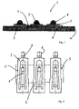
In der Zeichnung zeigt: -
Fig. 1 eine Seitenansicht der erfindungsgemäßen Lötkontaktvorrichtung; -
Fig. 2 eine Draufsicht auf die Lötkontaktvorrichtung gemäßFig. 1 , - In den
Fig. 1 bis Fig. 2 ist eine Lötkontaktvorrichtung 1 montiert auf eine Leiterplatte 10 gezeigt. In dem inFig. 1 gezeigten Zustand ist die Folie 2, welche zwischen den Kontakten 3 und der Leiterplatte 10 befindlich angeordnet ist, noch in einem nicht aufgeschmolzenen Zustand. - Nicht dargestellt ist die Situation nach dem Lötprozess, wo die Kontaktelemente 3 um eine definierte Distanz in Abhängigkeit von der Beschaffenheit der Folie 2 in Richtung der Oberfläche der Leiterplatte 10 gelangen und damit in eine definierte Abstandsposition, wobei gleichzeitig die Anschlussebenen der Kontaktelemente 3 mit der Leiterplatte 10 verlötet werden.
- In der in
Fig. 1 dargestellten Ausgangssituation bietet die Leiterplatte 10 eine Anzahl von nicht dargestellten Lötpads 11. Auf die Leiterplatte 10 wird die Lötkontaktiervorrichtung 1 aufgesetzt. Die erfindungsgemäße Lötkontaktiervorrichtung 1 umfasst drei paarweise zueinander beabstandete Kontaktelemente 3, welche mechanisch verbunden sind mit einer Folie 2, wobei im vorliegenden Beispiel die Folie 2 als Lötmaterialfolie 2 ausgestattet ist. Die Folie 2 kann aus einem beliebigen schmelzenden Material ausgebildet sein, welches gefüllt ist mit Lötmaterial. Wesentlich dabei ist, dass die Folie 2 formstabil bleibt und so ausgebildet ist, dass nach Befestigung der Kontaktelemente 3 mit der Folie 2 eine formstabile im wesentlichen ebene Kontaktiervorrichtung gebildet wird. Die Folie 2 kann In ihrer Dicke und Beschaffenheit so gewählt werden, dass sie nach dem Aufschmelzen durch Erwärmung den gewünschten Anteil an Lot und damit den gewünschten Abstand zur Leiterplatte 10 definiert. - Im vorliegenden Fall ist die Folie 2 ausgebildet aus einer gewalzten Lötfolie, welche im Reflowlötprozess aufschmilzt und die Verbindung der Kontaktelemente 3 mit dem Lötpads 11 der Leiterplatte 10 bildet.
- In der
Fig. 2 genauer dargestellt, sind die Kontaktelemente 3 mit ihrem Verbindungsabschnitt 5 auf der Folie 2. - Nicht dargestellt ist hier die Leiterplatte 10.
- Die Kontaktelemente 3 umfassen einen Kontaktelementrahmen 7, welcher an einem Ende die Kontaktfeder 6 umfasst, die wiederum federnd aus dem Kontaktelementrahmen 7 herausragt. An einem Ende des Kontaktelementrahmens 7 befinden sich je einen Kontaktlippe 8, welche so nach unten in Richtung zur Leiterplatte 10 gebogen ist, mit einem im wesentlichen flachen Unterteil 9, dass dies dem Abstand zur Leiterplatte definiert und damit die Foliendicke bestimmt.
-
- 1
- Lötkontaktvorrichtung
- 2
- Folie
- 3
- Kontaktelemente
- 4
- Lötflächen
- 5
- Verbindungsabschnitt
- 6
- Kontaktfedern
- 7
- Kontaktelementrahmen
- 8
- Kontaktlippen
- 9
- Kontaktlippenunterseite
- 10
- Leiterplatte
- 11
- Lötpads
Claims (7)
- Lötkontaktvorrichtung (1) zur elektrischen Verbindung mit einer Leiterplatte (10), umfassend mindestens zwei zueinander beabstandete Kontaktelemente (3), sowie eine im wesentlichen formstabile Folie (2), welche mit dem Kontaktelementen (3) mechanisch an deren Oberfläche verbunden ist, dadurch gekennzeichnet, dass die Folie (2) als schmelzbare Folie ausgebildet ist, welche sich bei Erhitzen bei eine typischen Löttemperatur verflüssigt und dabei die von der Folle gebildete Verbindung zwischen den Kontaktelementen getrennt wird.
- Lötkontaktvorrichtung (1) gemäß Anspruch 1, dadurch gekennzeichnet, dass die Folie (2) zumindest teilweise aus Lotmaterial besteht.
- Lötkontaktvorrichtung (1) gemäß Anspruch 1 oder 2, dadurch gekennzeichnet, dass die Folie (2) eine Lötfolie darstellt, die nahezu vollständig aus Lotmaterial hergestellt ist, vorzugsweise über 95 % Gewichtsanteil Lötmaterial umfasst.
- Lötkontaktvorrichtung (1) gemäß Anspruch 2 oder 3, dadurch gekennzeichnet, dass das Lotmaterial der Lötfolie vollständig und automatisch im Lötprozess als Verbindungslot an den Kontaktstellen zur Verbindung mit der Leiterplatte dient.
- Lötkontaktelement (3) gemäß Anspruch 1 bis 4, dadurch gekennzeichnet, dass die Kontaktelemente (3) einen Kontaktelementrahmen (7) umfassen mit einem Verbindungsabschnitt (5), welcher mit der Oberfläche der Folle (2) verbunden Ist.
- Lötkontaktvorrichtung (1) gemäß einem der vorhergehenden Ansprüche, dadurch gekennzeichnet, dass die Kontaktelemente (3) über eine Kontaktlippe (8) verfügen, welche mit ihrer Kontaktlippenunterseite (9) eine Ebene mit der Folie (2) aufspannen und bilden.
- Verfahren zur Herstellung einer Lötkontaktvorrichtung (1) gemäß einem der Ansprüche 1 bis 6, umfassend die folgenden Schritte:a) Bereitstellen einer im wesentlichen formstabilen schmelzbaren Folie (2), welche zumindest teilweise aus Lotmaterial ausgebildet ist;b) Bereitstellen von mindestens zwei paarweise beabstandeten Kontaktelementen (3) mit Verbindungsabschnitten (5) an den Kontaktelementen (3);c) Verbinden der Kontaktelemente (3) mit ihren Verbindungsabschnitten (5) mit der Oberfläche der Folie (2).
Applications Claiming Priority (1)
| Application Number | Priority Date | Filing Date | Title |
|---|---|---|---|
| DE102008035056.7A DE102008035056B4 (de) | 2008-07-26 | 2008-07-26 | Verfahren zur Herstellung einer Lötkontaktvorrichtung |
Publications (2)
| Publication Number | Publication Date |
|---|---|
| EP2148395A2 true EP2148395A2 (de) | 2010-01-27 |
| EP2148395A3 EP2148395A3 (de) | 2011-03-09 |
Family
ID=41165611
Family Applications (1)
| Application Number | Title | Priority Date | Filing Date |
|---|---|---|---|
| EP09006656A Withdrawn EP2148395A3 (de) | 2008-07-26 | 2009-05-18 | Lötkontaktvorrichtung |
Country Status (2)
| Country | Link |
|---|---|
| EP (1) | EP2148395A3 (de) |
| DE (1) | DE102008035056B4 (de) |
Citations (1)
| Publication number | Priority date | Publication date | Assignee | Title |
|---|---|---|---|---|
| DE102006005275A1 (de) | 2006-02-06 | 2007-08-09 | Amphenol-Tuchel Electronics Gmbh | Superflacher Simblock |
Family Cites Families (1)
| Publication number | Priority date | Publication date | Assignee | Title |
|---|---|---|---|---|
| JPH03289192A (ja) * | 1990-04-05 | 1991-12-19 | Matsushita Electric Ind Co Ltd | プリント配線基板上における部品のはんだ付け方法 |
-
2008
- 2008-07-26 DE DE102008035056.7A patent/DE102008035056B4/de not_active Expired - Fee Related
-
2009
- 2009-05-18 EP EP09006656A patent/EP2148395A3/de not_active Withdrawn
Patent Citations (1)
| Publication number | Priority date | Publication date | Assignee | Title |
|---|---|---|---|---|
| DE102006005275A1 (de) | 2006-02-06 | 2007-08-09 | Amphenol-Tuchel Electronics Gmbh | Superflacher Simblock |
Also Published As
| Publication number | Publication date |
|---|---|
| EP2148395A3 (de) | 2011-03-09 |
| DE102008035056A1 (de) | 2010-02-18 |
| DE102008035056B4 (de) | 2014-03-20 |
Similar Documents
| Publication | Publication Date | Title |
|---|---|---|
| EP0948815B1 (de) | Chipmodul und verfahren zur herstellung eines chipmoduls | |
| DE102004050588B4 (de) | Anordnung mit einem Leistungshalbleiterbauelement und mit einer Kontakteinrichtung | |
| EP0863530A2 (de) | Leiterplatte für elektrische Schaltungen und Verfahren zur Herstellung einer solchen Leiterplatte | |
| DE102006016775A1 (de) | Elektronische Vorrichtung und Verfahren zum Herstellen der Gleichen | |
| EP0902973A1 (de) | Trägerelement für einen halbleiterchip | |
| DE69805404T2 (de) | Verfahren zum herstellen kontaktloser karten mit antennenverbindung durch gelötete drähte | |
| DE102013105571A1 (de) | Kontaktelement zur Kontaktierung mindestens eines Wicklungsdrahts | |
| DE19541072A1 (de) | Chipmodul | |
| DE4130899C2 (de) | Halbleitervorrichtung | |
| EP1028388B1 (de) | Identifizierungselement und Verfahren zur Herstellung eines Identifizierungselements | |
| EP1034555A1 (de) | Halbleiterbauelement mit definiertem verhalten bei einem ausfall und verfahren zur herstellung eines solchen | |
| DE102008041035A1 (de) | Elektronischer Sensor oder Sensorgerät, insbesondere Beschleunigungssensor, mit einem in ein Sensorgehäuse eingebauten Chipmodul | |
| DE102005017849B4 (de) | Elektronisches Bauteil | |
| EP1714533B1 (de) | Elektrische baugruppe mit einem elektrisch leitfähigen kontaktstift zum einpressen in eine öffnung einer leiterplatte | |
| EP3132496B1 (de) | Antennenplatine für die oberflächenmontage | |
| EP2305010B1 (de) | Elektrische schaltungsanordnung | |
| EP2148395A2 (de) | Lötkontaktvorrichtung | |
| DE2249209A1 (de) | Leiterrahmen zur verwendung in gehaeusen fuer halbleiterbauelemente | |
| DE112015003364T5 (de) | Schaltungsanordnung | |
| DE102006058695B4 (de) | Leistungshalbleitermodul mit stumpf gelötetem Anschlusselement | |
| EP2343780A1 (de) | Halbleiterschaltungsanordnung | |
| DE10157113A1 (de) | Elektronische Baugruppe | |
| DE69206977T2 (de) | Kontaktvorrichtung für ein elektrisches oder elektronisches bauteil | |
| DE10133959B4 (de) | Elektronisches Bauteil mit Halbleiterchip | |
| DE19502157A1 (de) | Trägerelement für einen IC-Baustein zum Einbau in Chipkarten und Verfahren zur Herstellung desselben |
Legal Events
| Date | Code | Title | Description |
|---|---|---|---|
| PUAI | Public reference made under article 153(3) epc to a published international application that has entered the european phase |
Free format text: ORIGINAL CODE: 0009012 |
|
| AK | Designated contracting states |
Kind code of ref document: A2 Designated state(s): AT BE BG CH CY CZ DE DK EE ES FI FR GB GR HR HU IE IS IT LI LT LU LV MC MK MT NL NO PL PT RO SE SI SK TR |
|
| AX | Request for extension of the european patent |
Extension state: AL BA RS |
|
| PUAL | Search report despatched |
Free format text: ORIGINAL CODE: 0009013 |
|
| AK | Designated contracting states |
Kind code of ref document: A3 Designated state(s): AT BE BG CH CY CZ DE DK EE ES FI FR GB GR HR HU IE IS IT LI LT LU LV MC MK MT NL NO PL PT RO SE SI SK TR |
|
| AX | Request for extension of the european patent |
Extension state: AL BA RS |
|
| 17P | Request for examination filed |
Effective date: 20110819 |
|
| 17Q | First examination report despatched |
Effective date: 20141218 |
|
| STAA | Information on the status of an ep patent application or granted ep patent |
Free format text: STATUS: THE APPLICATION IS DEEMED TO BE WITHDRAWN |
|
| 18D | Application deemed to be withdrawn |
Effective date: 20161201 |