EP3132496B1 - Antennenplatine für die oberflächenmontage - Google Patents
Antennenplatine für die oberflächenmontage Download PDFInfo
- Publication number
- EP3132496B1 EP3132496B1 EP15714438.7A EP15714438A EP3132496B1 EP 3132496 B1 EP3132496 B1 EP 3132496B1 EP 15714438 A EP15714438 A EP 15714438A EP 3132496 B1 EP3132496 B1 EP 3132496B1
- Authority
- EP
- European Patent Office
- Prior art keywords
- antenna
- circuit board
- printed circuit
- face
- solder
- Prior art date
- Legal status (The legal status is an assumption and is not a legal conclusion. Google has not performed a legal analysis and makes no representation as to the accuracy of the status listed.)
- Active
Links
- 238000005516 engineering process Methods 0.000 title claims description 11
- 229910000679 solder Inorganic materials 0.000 claims description 25
- 238000005476 soldering Methods 0.000 claims description 20
- 238000000034 method Methods 0.000 claims description 12
- 238000002844 melting Methods 0.000 claims description 2
- 230000008018 melting Effects 0.000 claims description 2
- 239000000758 substrate Substances 0.000 description 5
- 238000013461 design Methods 0.000 description 3
- 239000004020 conductor Substances 0.000 description 2
- 238000004519 manufacturing process Methods 0.000 description 2
- 238000001465 metallisation Methods 0.000 description 2
- 238000012544 monitoring process Methods 0.000 description 2
- 238000012545 processing Methods 0.000 description 2
- 239000000853 adhesive Substances 0.000 description 1
- 230000001070 adhesive effect Effects 0.000 description 1
- 230000005540 biological transmission Effects 0.000 description 1
- 230000001419 dependent effect Effects 0.000 description 1
- 239000003989 dielectric material Substances 0.000 description 1
- 238000010438 heat treatment Methods 0.000 description 1
- 238000009434 installation Methods 0.000 description 1
- 230000005226 mechanical processes and functions Effects 0.000 description 1
- 238000010295 mobile communication Methods 0.000 description 1
- 229920003002 synthetic resin Polymers 0.000 description 1
- 239000000057 synthetic resin Substances 0.000 description 1
Images
Classifications
-
- H—ELECTRICITY
- H01—ELECTRIC ELEMENTS
- H01Q—ANTENNAS, i.e. RADIO AERIALS
- H01Q1/00—Details of, or arrangements associated with, antennas
- H01Q1/27—Adaptation for use in or on movable bodies
- H01Q1/32—Adaptation for use in or on road or rail vehicles
- H01Q1/325—Adaptation for use in or on road or rail vehicles characterised by the location of the antenna on the vehicle
- H01Q1/3275—Adaptation for use in or on road or rail vehicles characterised by the location of the antenna on the vehicle mounted on a horizontal surface of the vehicle, e.g. on roof, hood, trunk
-
- H—ELECTRICITY
- H01—ELECTRIC ELEMENTS
- H01Q—ANTENNAS, i.e. RADIO AERIALS
- H01Q1/00—Details of, or arrangements associated with, antennas
- H01Q1/36—Structural form of radiating elements, e.g. cone, spiral, umbrella; Particular materials used therewith
- H01Q1/38—Structural form of radiating elements, e.g. cone, spiral, umbrella; Particular materials used therewith formed by a conductive layer on an insulating support
-
- H—ELECTRICITY
- H01—ELECTRIC ELEMENTS
- H01Q—ANTENNAS, i.e. RADIO AERIALS
- H01Q9/00—Electrically-short antennas having dimensions not more than twice the operating wavelength and consisting of conductive active radiating elements
- H01Q9/04—Resonant antennas
- H01Q9/30—Resonant antennas with feed to end of elongated active element, e.g. unipole
- H01Q9/42—Resonant antennas with feed to end of elongated active element, e.g. unipole with folded element, the folded parts being spaced apart a small fraction of the operating wavelength
Definitions
- the invention relates to a method for assembling an antenna module and an antenna module.
- Such antenna modules are used, for example, to provide radio services such as radio reception (analog, digital), television reception (analog, digital), mobile communications (GMS bands, UMTS, LTE), GPS information, vehicle access control system, immobilizer control, enabling engine start, implementation of personal settings, interior monitoring, parking assistance, tire pressure monitoring, auxiliary heating, remote start, Bluetooth, WLAN, etc.
- Such antenna modules are usually arranged on the vehicle roof and, in addition to one or more PCB antennas, also include transmitting and receiving circuits (transceiver circuits) which are arranged on one or more electronic boards.
- One or more PCB antennas are connected to one of the electronic boards (printed circuit boards) (e.g. by soldering).
- a PCB antenna has milled pins on the edge of the board, which are inserted through corresponding openings in the electronic board to which the PCB antenna is to be attached, so that the PCB antenna is perpendicular to the electronic board.
- inserting the PCB board into the openings of the electronic board is usually done manually.
- the PCB antenna is then soldered to the electronic board on the pins inserted into the electronic board using a selective soldering process or with the help of a soldering robot.
- This process required for the through hole technology (THT) of the antenna is - compared to other assembly and soldering processes
- SMT Surface mounting technology
- An antenna comprising an antenna element and a carrier, the antenna element being provided in a region of the carrier, is disclosed GB 2 474 595 A .
- a dielectric antenna module having an antenna element unit in which an electrode and a signal line are formed on a dielectric carrier, and a module carrier unit in which a signal processing circuit is formed.
- the antenna element unit and the module carrier unit are arranged and connected to one another in such a way that bottom surfaces of the antenna element unit and the module carrier unit lie in a single plane.
- a radio antenna assembly with a circuit board and a radio antenna component is disclosed WO 2008/001169 A2 .
- the circuit board has a recess
- the radio antenna component has a radiator element arranged on the circuit board, with at least part of the radiator element being arranged in the recess.
- the circuit board antenna includes a main circuit board having a plurality of openings and an erect circuit board orthogonally attached to the main circuit board and having a plurality of protrusions.
- One of the holes is a line hole and one of the protrusions is a line protrusion.
- the line projection is inserted into the line opening.
- An antenna structure including a first substrate having a through hole and a second substrate is provided EP 2 538 489 A1 known.
- the second substrate has a Mounting plate that is connectable to the through hole such that the first substrate and the second substrate are in an orthogonal configuration.
- the object on which the invention is based is to provide a method for assembling an antenna module and an antenna module, which enables reliable and correct assembly of a circuit board with an antenna. This object is achieved by a method according to claim 1 and an antenna module according to claim 2. An exemplary embodiment is the subject of the dependent claim.
- An antenna arrangement is described below which has a circuit board with a front and a back as well as an antenna structure arranged on the front and/or the back.
- the antenna arrangement further comprises at least one metallized contact surface for surface mounting on a surface of a printed circuit board, which is arranged on an end face of the circuit board and is electrically connected to the antenna structure.
- SMT surface mounting technology
- the front side of the circuit board has an edge towards the front and an edge towards the back, whereby the at least one metallized contact surface can at least partially surround both edges.
- the antenna board can have a projection on its front side, which can be pushed through a corresponding opening (a slot) in the circuit board. This enables a reliable and correct arrangement of the antenna structure on the circuit board before soldering.
- the projection mentioned can, but does not have to, have any metallization since it does not fulfill any electrical function.
- the method includes providing a circuit board with at least one soldering pad and that Providing an antenna arrangement as described above. Solder paste is applied to the soldering pad and the antenna arrangement is arranged on the circuit board so that the at least metallized contact surface on the end face of the antenna board contacts the soldering pad and lies flat against it. Finally, the solder connection between the circuit board and the antenna arrangement is created by melting the solder paste.
- the antenna arrangement can be processed automatically in a similar way to conventional SMD components.
- a projection located on the front side of the antenna is inserted through a through hole (a slot) in the circuit board.
- the solder connection is made, for example, using reflow soldering.
- an antenna module has a circuit board with at least one soldering pad and an antenna that includes a circuit board with a front and a back.
- An antenna structure is arranged on the front and/or back of the circuit board.
- On the front side of the circuit board there is at least one metallized contact surface, which is electrically connected to the antenna structure.
- the contact surface arranged on one end face of the circuit board lies flat against the soldering pad and is attached to it by means of a solder connection.
- SMT surface mount technology
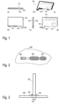
- FIG 1 An example of a PCB antenna 100 is shown, which is designed for mounting on a circuit board (see Figure 2 ) is designed using a surface mounting technology.
- the circuit board can be part of an antenna module, which z. B. can be arranged in or on a vehicle roof as described above.
- Figure 1a shows a view of the lower face of the antenna
- Figure 1b a view of the back 102
- Figure 1c a side view
- Figure 1d a view of the front 101 with the antenna structure 110 arranged thereon
- Figure 1e an isometric representation.
- the technique for mounting components on the surface of a circuit board is also known as Surface Mounting Technology (SMT).
- PCB antennas are realized with the help of conductor tracks arranged on a circuit board.
- the circuit board 100 is made of a dielectric material, for example fiber-reinforced synthetic resin (e.g. FR-4 or the like).
- An antenna structure 110 is arranged on a front 101 or a back 102.
- the antenna structure 110 is formed by strip conductors arranged on the circuit board, the geometric configuration of which is designed depending on the desired transmission/reception properties.
- the antenna structure 110 can also extend over the front and back 101, 102 of the circuit board 100.
- Several separate antenna structures 110 can also be arranged on the circuit board 100, for example for receiving radio signals in different frequency ranges.
- the lower end face has at least one metallized contact surface.
- two metallized contact surfaces 120 and 121 are provided on the front side (in Fig. 1a shown hatched).
- the contact surfaces can be tin-plated.
- the metallized contact surfaces are not only located on the front side of the circuit board 100, but can also enclose the edge to the front 101 and the edge to the back 102 (see Fig. 1b and 1d) .
- the metallized contact surfaces 120 and 121 are connected to the antenna structure.
- contact surfaces necessarily have to fulfill an electrical function and be electrically connected to the antenna structure 110.
- the contact pad of a circuit board can also fulfill a purely mechanical function, i.e. ensure a mechanically stable connection between the antenna and the circuit board.
- FIG 2 a part of a circuit board 200 is shown, on which the PCB antenna according to Figure 1 is mounted.
- the PCB antenna 100 is arranged on the circuit board 200 in such a way that the contact surfaces 120 and 121 on the front side of the antenna circuit board 100 lie flat on corresponding solder pads 220 and 221 of the circuit board.
- a solder paste is usually applied to the solder pads to enable subsequent reflow soldering. So that the antenna board 100 is fixed approximately vertically on the circuit board 200 before soldering and cannot slip or fall over, the antenna can be glued to the circuit board 200, for example.
- the adhesive is applied to the circuit board 200 before it is assembled (before or after applying the solder paste or solder preforms).
- antennas can be installed according to the in Figure 1
- the example shown is provided in a belted form, which allows simple automatic processing.
- the antenna board 100 can have at least one projection 105 on its lower end face, which can be inserted into a corresponding slot 205 on the circuit board.
- the projection 105 can have metallization. However, this is not absolutely necessary since this projection 105 does not fulfill any electrical function, but only serves to hold the antenna in the correct target position on the circuit board 200 before soldering. Because the slot 205 is elongated (has the shape of an elongated hole) and the projection 105 has a corresponding rectangular cross section, the antenna board 100 is held in the slot 105 so that it cannot rotate.
- Figure 3 is a representation of a circuit board 200 and an antenna according to Figure 1 in assembled condition.
- the antenna can be processed like other SMD components, which enables a significant reduction in production costs. Installation is easier than with previous antenna designs; in particular, there is no need to manually equip the circuit board with the antenna. A complex selective soldering process is no longer necessary. Rather, the PCB antenna 100 can be connected to the circuit board 200 together with other SMD components, for example by means of reflow soldering (solder layer 230).
Landscapes
- Engineering & Computer Science (AREA)
- Remote Sensing (AREA)
- Support Of Aerials (AREA)
- Details Of Aerials (AREA)
- Combinations Of Printed Boards (AREA)
Description
- Die Erfindung betrifft ein Verfahren zur Assemblierung eines Antennenmoduls und ein Antennenmodul.
- Antennenplatinen, auch als PCB-Antennen bezeichnet (PCB = printed circuit board), werden häufig in Antennenmodulen in der Fahrzeugtechnik eingesetzt. Derartige Antennenmodule werden beispielsweise verwendet, um Funkdienste wie beispielsweise Rundfunkempfang (analog, digital), Fernsehempfang (analog, digital), Mobilfunk (GMS-Bänder, UMTS, LTE), GPS-Information, Fahrzeugzugangskontrollsystem, Steuerung der Wegfahrsperre, Freigabe des Motorstarts, Vornahme von persönlichen Einstellungen, Innenraumüberwachung, Parkhilfe, Reifendruckkontrolle, Standheizung, Fernstart, Bluetooth, WLAN, etc. zu ermöglichen. Derartige Antennenmodule (siehe beispielsweise
EP 1 903 632 B1 ) sind üblicherweise am Fahrzeugdach angeordnet und umfassen neben einer oder mehrerer PCB-Antennen auch Sende- und Empfangsschaltungen (Transceiver-Schaltungen), die auf einer oder mehreren Elektronikplatinen angeordnet sind. - Eine oder mehrere PCB-Antennen sind dabei mit einer der Elektronikplatinen (Leiterplatten) verbunden (z. B. durch Löten) . Eine PCB-Antenne weist dazu am Platinenrand ausgefräste Pins auf, die durch korrespondierende Öffnungen in der Elektronikplatine, an der die PCB-Antenne befestigt werden soll, gesteckt wird, so dass die PCB-Antenne senkrecht zur Elektronikplatine steht. Das Einstecken der PCB-Platine in die Öffnungen der Elektronikplatine erfolgt bei der Produktion der Antennenmodule meist manuell. Die PCB-Antenne wird anschließend an den in die Elektronikplatine eingesteckten Pins mittels eines selektiven Lötverfahrens oder mit Hilfe eines Lötroboters mit der Elektronikplatine verlötet. Dieser für die Durchsteckmontage (THT, through hole technology) der Antenne notwendige Prozess ist - verglichen mit anderen Bestückungs- und Lötverfahren zur Oberflächenmontage (SMT, surface mounting technology), die beispielsweise bei SMD(surface mounted device)-Bauteilen verwendet werden können - zeitaufwändig und kostspielig.
- Eine Antenne, die ein Antennenelement und einen Träger aufweist, wobei das Antennenelement in einem Bereich des Trägers vorgesehen ist, offenbart
GB 2 474 595 A - Aus
US 2005/017902 A1 ist ein dielektrisches Antennenmodul mit einer Antennenelementeinheit, in der eine Elektrode und eine Signalleitung auf einem dielektrischen Träger ausgebildet sind, und einer Modulträgereinheit, in der eine Signalverarbeitungsschaltung ausgebildet ist, bekannt. Die Antennenelementeinheit und die Modulträgereinheit sind so angeordnet und miteinander verbunden, dass Bodenflächen der Antennenelementeinheit und der Modulträgereinheit in einer einzigen Ebene liegen. - Eine Funkantennenanordnung mit einer Leiterplatte und einer Funkantennenkomponente offenbart
WO 2008/001169 A2 . Die Leiterplatte weist eine Ausnehmung auf, und die Funkantennenkomponente weist ein auf der Leiterplatte angeordnetes Strahlerelement auf, wobei zumindest ein Teil des Strahlerelements in der Ausnehmung angeordnet ist. - Aus
US 2011/122045 A1 ist eine Leiterplattenantenne bekannt. Die Leiterplattenantenne umfasst eine Hauptleiterplatte, die mehrere Durchbrechungen aufweist, und eine aufgerichtete Leiterplatte, die orthogonal an der Hauptleiterplatte befestigt ist und mehrere Vorsprünge aufweist. Eine der Durchbrechungen ist eine Leitungsdurchbrechung, und einer der Vorsprünge ist ein Leitungsvorsprung. Der Leitungsvorsprung ist in die Leitungsdurchbrechung eingesetzt. - Eine Antennenstruktur, die ein erstes Substrat, das ein Durchgangsloch aufweist, und ein zweites Substrat umfasst, ist aus
EP 2 538 489 A1 bekannt. Das zweite Substrat weist ein Montageplättchen auf, das mit dem Durchgangsloch derart verbindbar ist, dass sich das erste Substrat und das zweite Substrat in einer orthogonalen Konfiguration befinden. - Die der Erfindung zugrunde liegende Aufgabe besteht darin, ein Verfahren zur Assemblierung eines Antennenmoduls und ein Antennenmodul anzugeben, wobei eine zuverlässige und korrekte Bestückung einer Leiterplatte mit einer Antenne ermöglicht ist. Diese Aufgabe wird durch ein Verfahren gemäß Anspruch 1 und ein Antennenmodul gemäß Anspruch 2 gelöst. Ein Ausführungsbeispiel ist Gegenstand des abhängigen Anspruchs.
- Im Folgenden wird eine Antennenanordnung beschrieben, die eine Platine mit Vorder- und einer Rückseite aufweist sowie eine auf der Vorderseite und/oder der Rückseite angeordnete Antennenstruktur. Die Antennenanordnung umfasst weiter mindestens eine an einer Stirnseite der Platine angeordnete und mit der Antennenstruktur elektrisch verbundene metallisierte Kontaktfläche zur Oberflächenmontage an einer Oberfläche einer Leiterplatte. Durch eine derartige Ausgestaltung wird eine Montage der Antennenanordnung an einer Leiterplatte mittels Oberflächenmontagetechnik (SMT) ermöglicht.
- Die Stirnseite der Platine weist eine Kante zur Vorderseite und eine Kante zur Rückseite auf, wobei die mindestens eine metallisierte Kontaktfläche beide Kanten zumindest teilweise umgeben kann. Die Antennenplatine kann an ihrer Stirnseite einen Vorsprung aufweisen, der durch eine korrespondierende Öffnung (einen Schlitz) in der Leiterplatte durchsteckbar ist. Dadurch wird eine zuverlässige und korrekte Anordnung der Antennenstruktur an der Leiterplatte vor dem Löten ermöglicht. Der erwähnte Vorsprung kann, muss aber keine Metallisierung aufweisen, da er keine elektrische Funktion erfüllt.
- Des Weiteren wird ein Verfahren zur Assemblierung eines Antennenmoduls beschrieben. Das Verfahren umfasst das Bereitstellen einer Leiterplatte mit mindestens einem Lötpad sowie das Bereitstellen einer Antennenanordnung wie oben beschrieben. Auf das Lötpad wird Lötpaste aufgebracht und die Antennenanordnung wird an der Leiterplatte angeordnet, so dass die mindestens metallisierte Kontaktfläche auf der Stirnseite der Antennenplatine das Lötpad kontaktiert und flächig an diesem anliegt. Schließlich wird durch Aufschmelzen der Lötpaste die Lötverbindung zwischen der Leiterplatte und der Antennenanordnung hergestellt. Die Antennenanordnung kann dabei in ähnlicher Weise wie übliche SMD-Bauelemente automatisiert verarbeitet werden.
- Bei dem Anordnen der Antennenplatine an der Leiterplatte wird ein an der Stirnseite der Antenne befindlicher Vorsprung durch ein Durchgangsloch (einen Schlitz) in der Leiterplatte gesteckt. Dies ermöglicht eine zuverlässige und korrekte Bestückung der Leiterplatte mit der Antennenanordnung und verhindert ein ungewolltes Verdrehen oder Kippen der Antenne, die im Wesentlichen senkrecht zur Leiterplatte steht. Die Lötverbindung erfolgt beispielsweise mittels Reflow-Löten.
- Schließlich wird ein Antennenmodul beschrieben, das eine Leiterplatte mit mindestens einem Lötpad sowie eine Antenne aufweist, die eine Platine mit Vorder- und einer Rückseite umfasst. Auf der Vorderseite und/oder der Rückseite der Platine ist eine Antennenstruktur angeordnet. Auf der Stirnseite der Platine befindet sich mindestens eine metallisierte Kontaktfläche, welche mit der Antennenstruktur elektrisch verbunden ist. Die an einer Stirnseite der Platine angeordnete Kontaktfläche liegt flächig an dem Lötpad an und ist an diesem mittels einer Lötverbindung befestigt.
- Sämtliche elektrischen Verbindungen zwischen Antenne und Leiterplatte können mittels Oberflächenmontagetechnik (SMT) hergestellt werden, was eine signifikante Reduktion der Produktionskosten erlaubt.
- Die Erfindung wird nachfolgend anhand der in den Figuren der Zeichnungen dargestellten Ausführungsbeispiele näher erläutert. In den Abbildungen zeigt:
- Figur 1
- mehrere Ansichten eines Beispiels einer zur Oberflächenmontage geeigneten PCB-Antenne;
- Figur 2
- eine Draufsicht auf eine Elektronikplatine mit SMT-Lötpads für die Oberflächenmontage einer PCB-Antenne gemäß
Fig. 1 und - Figur 3
- eine Frontansicht der Elektronikplatine aus
Fig. 2 mit darauf mittels Oberflächenmontagetechnik befestigter PCB-Antenne. - In den Figuren bezeichnen gleiche Bezugszeichen gleiche oder ähnliche Komponenten mit gleicher oder ähnlicher Ausgestaltung oder Funktion.
- In
Figur 1 ist ein Beispiel einer PCB-Antenne 100 dargestellt, welche zur Montage auf einer Leiterplatte (sieheFigur 2 ) mittels einer Oberflächenmontagetechnik ausgestaltet ist. Die Leiterplatte kann Bestandteil eines Antennenmoduls sein, welches z. B. wie eingangs beschrieben in oder an einem Fahrzeugdach angeordnet sein kann.Figur 1a zeigt eine Ansicht der unteren Stirnseite der Antenne,Figur 1b eine Ansicht der Rückseite 102,Figur 1c eine Seitenansicht,Figur 1d eine Ansicht der Vorderseite 101 mit darauf angeordneter Antennenstruktur 110 undFigur 1e eine isometrische Darstellung. Die dargestellte PCB-Antenne kann daher als SMD-Bauelement (Surface Mounted Device = SMD) angesehen werden. SMD-Bauelemente haben im Gegensatz zu Bauelementen zur Durchsteckmontage (Through Hole Technology = THT) keine Anschlussdrähte oder Anschlussstifte, sondern werden mittels lötfähiger Anschlussflächen direkt auf korrespondierende Lötpads (Lötflächen) einer Leiterplatte gelötet. Die Technik zur Montage von Bauelementen an der Oberfläche einer Leiterplatte wird auch als Oberflächenmontagetechnik (Surface Mounting Technology = SMT) bezeichnet. - Allgemein sind PCB-Antennen mit Hilfe von auf einer Platine angeordneten Leiterbahnen realisiert. Im vorliegenden Fall besteht die Platine 100 aus einem dielektrischen Material, beispielsweise aus faserverstärktem Kunstharz (z. B. FR-4 oder ähnlichem). Auf einer Vorderseite 101 oder einer Rückseite 102 ist eine Antennenstruktur 110 angeordnet. Die Antennenstruktur 110 wird durch auf der Platine angeordnete Streifenleiter gebildet, deren geometrische Ausgestaltung abhängig von den gewünschten Sende-/und Empfangseigenschaften entworfen wird. Die Antennenstruktur 110 kann sich auch über die Vorder- und die Rückseite 101, 102 der Platine 100 erstrecken. Auf der Platine 100 können auch mehrere separate Antennenstrukturen 110 angeordnet sein, beispielsweise zum Empfang von Funksignalen in unterschiedlichen Frequenzbereichen.
- Zur elektrischen Verbindung der Antenne mit einer Leiterplatte weist die untere Stirnseite mindestens eine metallisierte Kontaktfläche auf. Im vorliegenden Beispiel sind auf der Stirnseite zwei metallisierte Kontaktflächen 120 und 121 vorgesehen (in
Fig. 1a schraffiert dargestellt). Um die Kontaktflächen besser mit korrespondierenden Lötpads einer Leiterplatte mittels Löten verbinden zu können, können die Kontaktflächen verzinnt sein. Die metallisierten Kontaktflächen befinden sich nicht nur auf der Stirnseite der Platine 100, sondern können auch die Kante zur Vorderseite 101 sowie die Kante zur Rückseite 102 umschließen (sieheFig. 1b und 1d) . Auf der Vorderseite 101 (und ggf. auch auf der Rückseite 102) der Platine 100 sind die metallisierten Kontaktflächen 120 und 121 mit der Antennenstruktur verbunden. - Nicht alle Kontaktflächen müssen zwangsläufig eine elektrische Funktion erfüllen und mit der Antennenstruktur 110 elektrisch verbunden sein. Eine Lötverbindung zwischen einer Kontaktfläche an der Stirnseite der Platine 100 und dem korrespondierenden Kontaktpad einer Leiterplatte kann auch eine rein mechanische Funktion erfüllen, d. h. eine mechanisch stabile Verbindung zwischen Antenne und Leiterplatte gewährleisten.
- In
Figur 2 ist ein Teil einer Leiterplatte 200 dargestellt, an dem die PCB-Antenne gemäßFigur 1 montiert wird. Die PCB-Antenne 100 wird derart an der Leiterplatte 200 angeordnet, dass die Kontaktflächen 120 und 121 an der Stirnseite der Antennenplatine 100 an korrespondierenden Lötpads 220 und 221 der Leiterplatte flächig anliegen. Vor der Montage wird auf die Lötpads üblicherweise eine Lötpaste aufgetragen, um das anschließende Reflow-Löten zu ermöglichen. Damit die Antennenplatine 100 vor dem Löten annähernd senkrecht auf der Leiterplatte 200 fixiert ist und nicht verrutschen oder umfallen kann, kann die Antenne beispielsweise an der Leiterplatte 200 angeklebt sein. Der Kleber wird dabei, wie bei der Oberflächenmontage üblich, vor dem Bestücken der Leiterplatte 200 auf diese aufgetragen (vor oder nach dem Auftragen der Lötpaste oder von Lot-Preforms) . Für die anschließende automatische Bestückung können Antennen gemäß dem inFigur 1 dargestellten Beispiel gegurtet zur Verfügung gestellt werden, was eine einfache automatische Verarbeitung erlaubt. - Um eine einfache und korrekte Platzierung der Antennenplatine 100 auf der gewünschten Stelle einer Leiterplatte 200 zu gewährleisten, kann die Antennenplatine 100 zumindest einen Vorsprung 105 an ihrer unteren Stirnseite aufweisen, welcher in einen korrespondierenden Schlitz 205 der Leiterplatte einsteckbar ist. Der Vorsprung 105 kann eine Metallisierung aufweisen. Dies ist jedoch nicht zwangsläufig notwendig, da dieser Vorsprung 105 keine elektrische Funktion erfüllt, sondern lediglich dazu dient, vor dem Löten die Antenne in der korrekten Sollposition an der Leiterplatte 200 zu halten. Dadurch, dass der Schlitz 205 länglich ist (die Form eines Langlochs hat) und der Vorsprung 105 einen entsprechenden rechteckigen Querschnitt aufweist, wird die Antennenplatine 100 verdrehsicher in dem Schlitz 105 gehalten.
Figur 3 ist eine Darstellung einer Leiterplatte 200 und einer Antenne gemäßFigur 1 in montiertem Zustand. - Durch die hier beschriebene Ausgestaltung der PCB-Antenne 100 kann die Antenne wie andere SMD-Bauelemente verarbeitet werden, was eine signifikante Reduktion der Produktionskosten ermöglicht. Die Montage gestaltet sich einfacher als bei bisherigen Antennenbauformen, insbesondere entfällt eine manuelle Bestückung der Leiterplatte mit der Antenne. Ein aufwändiges selektives Lötverfahren ist nicht mehr notwendig. Vielmehr kann die PCB-Antenne 100 zusammen mit anderen SMD-Komponenten beispielsweise mittels Reflow-Löten (Lotschicht 230) mit der Leiterplatte 200 verbunden werden.
Claims (3)
- Verfahren zur Assemblierung eines Antennenmoduls, das Folgendes umfasst:- Bereitstellen einer Leiterplatte (200) mit mindestens einem Lötpad (220, 221);- Bereitstellen einer Antenne, die
aufweist:- eine Platine (100) mit Vorder- und einer Rückseite (101, 102) und einer auf der Vorderseite (101) oder der Rückseite (102) oder sowohl auf der Vorderseite (101) als auch der Rückseite (102) angeordneten Antennenstruktur (110);- mindestens eine an einer Stirnseite der Platine (100) angeordnete und mit der Antennenstruktur (110) elektrisch verbundene metallisierte Kontaktfläche (120, 121) zur Oberflächenmontage an einer Oberfläche einer Leiterplatte (200);- Aufbringen von Lötpaste auf das mindestens eine Lötpad (220, 221);- Anordnen der Antenne (100) an der Leiterplatte (200), so dass die mindestens eine metallisierte Kontaktfläche (120, 121) auf der Stirnseite der Platine (200) der Antenne das mindestens eine Lötpad (220, 221) kontaktiert und flächig an diesem anliegt und wobei das Anordnen der Antenne an der Leiterplatte (200) ein Durchstecken eines Vorsprungs (105) an der Stirnseite der Antenne (100) durch ein Durchgangsloch (205) in der Leiterplatte (200) umfasst, so dass ein ungewolltes Verdrehen oder Kippen der Antenne verhindert ist, und wobei die Antenne im Wesentlichen senkrecht zur Leiterplatte (200) steht;- Herstellen der Lötverbindung durch Aufschmelzen der Lötpaste, wobei die Lötverbindung mittels Reflow-Löten hergestellt wird. - Antennenmodul, das Folgendes aufweist:- eine Leiterplatte (200) mit mindestens einem Lötpad;- eine Antenne umfassend eine Platine (100) mit Vorder- und einer Rückseite (101, 102), eine auf der Vorderseite (101) oder der Rückseite (102) oder sowohl auf der Vorderseite (101) als auch der Rückseite (102) angeordneten Antennenstruktur (110), sowie mindestens eine an einer Stirnseite der Platine (100) angeordnete und mit der Antennenstruktur (110) elektrisch verbundene metallisierte Kontaktfläche (120, 121);wobei die an einer Stirnseite der Platine (100) angeordnete Kontaktfläche (120, 121) flächig an dem Lötpad (220, 221) anliegt und an diesem mittels einer Lötverbindung, die mittels Reflow-Löten hergestellt ist, befestigt ist und wobei die Leiterplatte (200) ein Durchgangsloch (205) neben dem mindestens einen Lötpad (220, 221) aufweist, wobei die Antenne an der Stirnseite der Platine (100) einen Vorsprung (105) aufweist, der durch das Durchgangsloch (205) in der Leiterplatte (200) eingesteckt ist, und wobei die Antenne im Wesentlichen senkrecht zur Leiterplatte (200) steht.
- Antennenmodul gemäß Anspruch 2, bei dem sämtliche elektrischen Verbindungen zwischen Antenne (100) und Leiterplatte (200) mittels Oberflächenmontagetechnik (SMT) hergestellt sind.
Applications Claiming Priority (2)
| Application Number | Priority Date | Filing Date | Title |
|---|---|---|---|
| DE102014207148.8A DE102014207148A1 (de) | 2014-04-14 | 2014-04-14 | Antennenplatine für die Oberflächenmontage |
| PCT/EP2015/056075 WO2015158500A1 (de) | 2014-04-14 | 2015-03-23 | Antennenplatine für die oberflächenmontage |
Publications (2)
| Publication Number | Publication Date |
|---|---|
| EP3132496A1 EP3132496A1 (de) | 2017-02-22 |
| EP3132496B1 true EP3132496B1 (de) | 2024-01-24 |
Family
ID=52814073
Family Applications (1)
| Application Number | Title | Priority Date | Filing Date |
|---|---|---|---|
| EP15714438.7A Active EP3132496B1 (de) | 2014-04-14 | 2015-03-23 | Antennenplatine für die oberflächenmontage |
Country Status (3)
| Country | Link |
|---|---|
| EP (1) | EP3132496B1 (de) |
| DE (1) | DE102014207148A1 (de) |
| WO (1) | WO2015158500A1 (de) |
Families Citing this family (4)
| Publication number | Priority date | Publication date | Assignee | Title |
|---|---|---|---|---|
| DE102015113224A1 (de) * | 2015-08-11 | 2017-02-16 | Endress + Hauser Gmbh + Co. Kg | Radar-Füllstandsmessgerät |
| US10931118B2 (en) | 2016-08-26 | 2021-02-23 | Nucurrent, Inc. | Wireless connector transmitter module with an electrical connector |
| JP6947657B2 (ja) | 2018-01-31 | 2021-10-13 | 株式会社デンソー | 電子回路 |
| EP3699558A1 (de) * | 2019-02-19 | 2020-08-26 | VEGA Grieshaber KG | Radarsenderanordnung mit integrierter antenne |
Family Cites Families (8)
| Publication number | Priority date | Publication date | Assignee | Title |
|---|---|---|---|---|
| US6295207B1 (en) * | 1999-10-12 | 2001-09-25 | 3Com Corporation | Retractable and removable extensions with edge plated PCB's in thin-profile electronic devices |
| AU2002366135A1 (en) * | 2001-11-20 | 2003-06-10 | Ube Industries, Ltd. | Dielectric antenna module |
| DE102006025176C5 (de) | 2006-05-30 | 2023-02-23 | Continental Automotive Technologies GmbH | Antennenmodul für ein Fahrzeug |
| US7619571B2 (en) * | 2006-06-28 | 2009-11-17 | Nokia Corporation | Antenna component and assembly |
| US8572841B2 (en) * | 2008-03-19 | 2013-11-05 | Harris Corporation | Printed wiring board assembly and related methods |
| GB2474595B (en) * | 2008-06-06 | 2012-10-03 | Murata Manufacturing Co | Antenna and radio communication apparatus |
| KR101675375B1 (ko) * | 2009-11-23 | 2016-11-14 | 삼성전자 주식회사 | 휴대단말기 내장용 pcb 안테나 |
| US8810457B2 (en) * | 2011-06-24 | 2014-08-19 | Taoglas Group Holdings | Orthogonal modular embedded antenna, with method of manufacture and kits therefor |
-
2014
- 2014-04-14 DE DE102014207148.8A patent/DE102014207148A1/de active Pending
-
2015
- 2015-03-23 EP EP15714438.7A patent/EP3132496B1/de active Active
- 2015-03-23 WO PCT/EP2015/056075 patent/WO2015158500A1/de active Application Filing
Also Published As
| Publication number | Publication date |
|---|---|
| WO2015158500A1 (de) | 2015-10-22 |
| EP3132496A1 (de) | 2017-02-22 |
| DE102014207148A1 (de) | 2015-10-15 |
Similar Documents
| Publication | Publication Date | Title |
|---|---|---|
| DE102011016294B4 (de) | Dachantenne, insbesondere Kraftfahrzeug-Dachantenne mit zugehöriger Steckverbindungseinrichtung | |
| EP1854168B1 (de) | Folienantenne für ein fahrzeug | |
| EP3132496B1 (de) | Antennenplatine für die oberflächenmontage | |
| DE10006530A1 (de) | Antennenfeder | |
| DE202010011837U1 (de) | Keramik-Patch-Antenne sowie auf einer Leiterplatine sitzende Keramik-Patch-Antenne | |
| DE102012007807A1 (de) | Tunermodul | |
| EP1393604B1 (de) | Leiterplatte mit einer darauf aufgebrachten kontakthülse | |
| EP2356722B1 (de) | Steckverbinder für schaltungsplatinen | |
| DE69813640T2 (de) | Elektrische verbinder | |
| DE102013222919A1 (de) | Verbinder und zugehöriges Halteelement | |
| EP2732509A1 (de) | Stecker und verfahren zu seiner herstellung | |
| DE102006009582B4 (de) | Elektronisches Gerät eines Fahrzeuges, insbesondere ein Antennenverstärker oder ein TV-Tuner, mit einem Aufnahmeraum für einen Steckverbinder | |
| DE102012112546A1 (de) | Verfahren zur Herstellung von mischbestückten Leiterplatten | |
| DE102005053973A1 (de) | Sensorbaugruppe | |
| DE102004041169B3 (de) | Anordnung und Verfahren zur Masseanbindung eines elektrischen Schaltungsträgers | |
| DE102004049575A1 (de) | Elektrisches Anschlusselement und Verfahren zum Anschließen eines Leiterkabels | |
| DE102018010157A1 (de) | Elektronisches Gerät, Baugruppe mit dem Gerät, Verfahren zum Montieren des Geräts und Verfahren zum Montieren der Baugruppe | |
| EP2309605A1 (de) | Steckdose für Telekommunikationsnetze | |
| DE102006037166B3 (de) | Fahrzeugantenne | |
| EP2166825A1 (de) | Lötbares elektronisches Modul mit Schaltungsträger | |
| DE102005006460A1 (de) | Kontaktpartner zur Montage auf einer Leiterplatte | |
| WO2015110658A1 (de) | Fahrzeugantennen mit einem flexiblen substrat als antennenträger | |
| DE102006058000B4 (de) | Platinenanordnung | |
| EP2197252B1 (de) | System mit skalierbarem Kamerakontaktblock, Verfahren zur Herstellung des Systems und Verfahren zum Einbau insbesondere einer SMD-Kamera in das Gehäuse eines Mobiltelefons | |
| DE202006012198U1 (de) | Fahrzeugantenne |
Legal Events
| Date | Code | Title | Description |
|---|---|---|---|
| STAA | Information on the status of an ep patent application or granted ep patent |
Free format text: STATUS: THE INTERNATIONAL PUBLICATION HAS BEEN MADE |
|
| PUAI | Public reference made under article 153(3) epc to a published international application that has entered the european phase |
Free format text: ORIGINAL CODE: 0009012 |
|
| STAA | Information on the status of an ep patent application or granted ep patent |
Free format text: STATUS: REQUEST FOR EXAMINATION WAS MADE |
|
| 17P | Request for examination filed |
Effective date: 20161114 |
|
| AK | Designated contracting states |
Kind code of ref document: A1 Designated state(s): AL AT BE BG CH CY CZ DE DK EE ES FI FR GB GR HR HU IE IS IT LI LT LU LV MC MK MT NL NO PL PT RO RS SE SI SK SM TR |
|
| AX | Request for extension of the european patent |
Extension state: BA ME |
|
| DAV | Request for validation of the european patent (deleted) | ||
| DAX | Request for extension of the european patent (deleted) | ||
| STAA | Information on the status of an ep patent application or granted ep patent |
Free format text: STATUS: EXAMINATION IS IN PROGRESS |
|
| 17Q | First examination report despatched |
Effective date: 20200325 |
|
| RAP1 | Party data changed (applicant data changed or rights of an application transferred) |
Owner name: CONTINENTAL AUTOMOTIVE GMBH |
|
| STAA | Information on the status of an ep patent application or granted ep patent |
Free format text: STATUS: EXAMINATION IS IN PROGRESS |
|
| STAA | Information on the status of an ep patent application or granted ep patent |
Free format text: STATUS: EXAMINATION IS IN PROGRESS |
|
| RAP1 | Party data changed (applicant data changed or rights of an application transferred) |
Owner name: CONTINENTAL AUTOMOTIVE TECHNOLOGIES GMBH |
|
| GRAP | Despatch of communication of intention to grant a patent |
Free format text: ORIGINAL CODE: EPIDOSNIGR1 |
|
| STAA | Information on the status of an ep patent application or granted ep patent |
Free format text: STATUS: GRANT OF PATENT IS INTENDED |
|
| INTG | Intention to grant announced |
Effective date: 20231019 |
|
| P01 | Opt-out of the competence of the unified patent court (upc) registered |
Effective date: 20231101 |
|
| GRAS | Grant fee paid |
Free format text: ORIGINAL CODE: EPIDOSNIGR3 |
|
| GRAA | (expected) grant |
Free format text: ORIGINAL CODE: 0009210 |
|
| STAA | Information on the status of an ep patent application or granted ep patent |
Free format text: STATUS: THE PATENT HAS BEEN GRANTED |
|
| AK | Designated contracting states |
Kind code of ref document: B1 Designated state(s): AL AT BE BG CH CY CZ DE DK EE ES FI FR GB GR HR HU IE IS IT LI LT LU LV MC MK MT NL NO PL PT RO RS SE SI SK SM TR |
|
| REG | Reference to a national code |
Ref country code: GB Ref legal event code: FG4D Free format text: NOT ENGLISH |
|
| REG | Reference to a national code |
Ref country code: CH Ref legal event code: EP |
|
| REG | Reference to a national code |
Ref country code: DE Ref legal event code: R096 Ref document number: 502015016741 Country of ref document: DE |
|
| REG | Reference to a national code |
Ref country code: IE Ref legal event code: FG4D Free format text: LANGUAGE OF EP DOCUMENT: GERMAN |
|
| REG | Reference to a national code |
Ref country code: DE Ref legal event code: R081 Ref document number: 502015016741 Country of ref document: DE Owner name: CONTINENTAL AUTOMOTIVE TECHNOLOGIES GMBH, DE Free format text: FORMER OWNER: CONTINENTAL AUTOMOTIVE TECHNOLOGIES GMBH, 30165 HANNOVER, DE |
|
| RAP4 | Party data changed (patent owner data changed or rights of a patent transferred) |
Owner name: CONTINENTAL AUTOMOTIVE TECHNOLOGIES GMBH |
|
| PGFP | Annual fee paid to national office [announced via postgrant information from national office to epo] |
Ref country code: DE Payment date: 20240331 Year of fee payment: 10 |
|
| REG | Reference to a national code |
Ref country code: CH Ref legal event code: PK Free format text: DIE PUBLIKATION VOM 27.03.2024 WURDE AM 24.04.2024 IRRTUEMLICHERWEISE ERNEUT PUBLIZIERT. LA PUBLICATION DU 27.03.2024 A ETE REPUBLIEE PAR ERREUR LE 24.04.2024. LA PUBBLICAZIONE DEL 27.03.2024 E STATA ERRONEAMENTE RIPUBBLICATA IL 24.04.2024. |
|
| REG | Reference to a national code |
Ref country code: LT Ref legal event code: MG9D |
|
| REG | Reference to a national code |
Ref country code: NL Ref legal event code: MP Effective date: 20240124 |
|
| PGFP | Annual fee paid to national office [announced via postgrant information from national office to epo] |
Ref country code: FR Payment date: 20240328 Year of fee payment: 10 Ref country code: BE Payment date: 20240320 Year of fee payment: 10 |
|
| PG25 | Lapsed in a contracting state [announced via postgrant information from national office to epo] |
Ref country code: NL Free format text: LAPSE BECAUSE OF FAILURE TO SUBMIT A TRANSLATION OF THE DESCRIPTION OR TO PAY THE FEE WITHIN THE PRESCRIBED TIME-LIMIT Effective date: 20240124 |
|
| PG25 | Lapsed in a contracting state [announced via postgrant information from national office to epo] |
Ref country code: NL Free format text: LAPSE BECAUSE OF FAILURE TO SUBMIT A TRANSLATION OF THE DESCRIPTION OR TO PAY THE FEE WITHIN THE PRESCRIBED TIME-LIMIT Effective date: 20240124 |
|
| PG25 | Lapsed in a contracting state [announced via postgrant information from national office to epo] |
Ref country code: IS Free format text: LAPSE BECAUSE OF FAILURE TO SUBMIT A TRANSLATION OF THE DESCRIPTION OR TO PAY THE FEE WITHIN THE PRESCRIBED TIME-LIMIT Effective date: 20240524 |
|
| PG25 | Lapsed in a contracting state [announced via postgrant information from national office to epo] |
Ref country code: LT Free format text: LAPSE BECAUSE OF FAILURE TO SUBMIT A TRANSLATION OF THE DESCRIPTION OR TO PAY THE FEE WITHIN THE PRESCRIBED TIME-LIMIT Effective date: 20240124 |
|
| PG25 | Lapsed in a contracting state [announced via postgrant information from national office to epo] |
Ref country code: GR Free format text: LAPSE BECAUSE OF FAILURE TO SUBMIT A TRANSLATION OF THE DESCRIPTION OR TO PAY THE FEE WITHIN THE PRESCRIBED TIME-LIMIT Effective date: 20240425 |
|
| PG25 | Lapsed in a contracting state [announced via postgrant information from national office to epo] |
Ref country code: RS Free format text: LAPSE BECAUSE OF FAILURE TO SUBMIT A TRANSLATION OF THE DESCRIPTION OR TO PAY THE FEE WITHIN THE PRESCRIBED TIME-LIMIT Effective date: 20240424 Ref country code: HR Free format text: LAPSE BECAUSE OF FAILURE TO SUBMIT A TRANSLATION OF THE DESCRIPTION OR TO PAY THE FEE WITHIN THE PRESCRIBED TIME-LIMIT Effective date: 20240124 |
|
| PG25 | Lapsed in a contracting state [announced via postgrant information from national office to epo] |
Ref country code: ES Free format text: LAPSE BECAUSE OF FAILURE TO SUBMIT A TRANSLATION OF THE DESCRIPTION OR TO PAY THE FEE WITHIN THE PRESCRIBED TIME-LIMIT Effective date: 20240124 |
|
| PG25 | Lapsed in a contracting state [announced via postgrant information from national office to epo] |
Ref country code: RS Free format text: LAPSE BECAUSE OF FAILURE TO SUBMIT A TRANSLATION OF THE DESCRIPTION OR TO PAY THE FEE WITHIN THE PRESCRIBED TIME-LIMIT Effective date: 20240424 Ref country code: NO Free format text: LAPSE BECAUSE OF FAILURE TO SUBMIT A TRANSLATION OF THE DESCRIPTION OR TO PAY THE FEE WITHIN THE PRESCRIBED TIME-LIMIT Effective date: 20240424 Ref country code: LT Free format text: LAPSE BECAUSE OF FAILURE TO SUBMIT A TRANSLATION OF THE DESCRIPTION OR TO PAY THE FEE WITHIN THE PRESCRIBED TIME-LIMIT Effective date: 20240124 Ref country code: IS Free format text: LAPSE BECAUSE OF FAILURE TO SUBMIT A TRANSLATION OF THE DESCRIPTION OR TO PAY THE FEE WITHIN THE PRESCRIBED TIME-LIMIT Effective date: 20240524 Ref country code: HR Free format text: LAPSE BECAUSE OF FAILURE TO SUBMIT A TRANSLATION OF THE DESCRIPTION OR TO PAY THE FEE WITHIN THE PRESCRIBED TIME-LIMIT Effective date: 20240124 Ref country code: GR Free format text: LAPSE BECAUSE OF FAILURE TO SUBMIT A TRANSLATION OF THE DESCRIPTION OR TO PAY THE FEE WITHIN THE PRESCRIBED TIME-LIMIT Effective date: 20240425 Ref country code: FI Free format text: LAPSE BECAUSE OF FAILURE TO SUBMIT A TRANSLATION OF THE DESCRIPTION OR TO PAY THE FEE WITHIN THE PRESCRIBED TIME-LIMIT Effective date: 20240124 Ref country code: ES Free format text: LAPSE BECAUSE OF FAILURE TO SUBMIT A TRANSLATION OF THE DESCRIPTION OR TO PAY THE FEE WITHIN THE PRESCRIBED TIME-LIMIT Effective date: 20240124 Ref country code: BG Free format text: LAPSE BECAUSE OF FAILURE TO SUBMIT A TRANSLATION OF THE DESCRIPTION OR TO PAY THE FEE WITHIN THE PRESCRIBED TIME-LIMIT Effective date: 20240124 |
|
| PG25 | Lapsed in a contracting state [announced via postgrant information from national office to epo] |
Ref country code: PT Free format text: LAPSE BECAUSE OF FAILURE TO SUBMIT A TRANSLATION OF THE DESCRIPTION OR TO PAY THE FEE WITHIN THE PRESCRIBED TIME-LIMIT Effective date: 20240524 Ref country code: PL Free format text: LAPSE BECAUSE OF FAILURE TO SUBMIT A TRANSLATION OF THE DESCRIPTION OR TO PAY THE FEE WITHIN THE PRESCRIBED TIME-LIMIT Effective date: 20240124 |
|
| PG25 | Lapsed in a contracting state [announced via postgrant information from national office to epo] |
Ref country code: SE Free format text: LAPSE BECAUSE OF FAILURE TO SUBMIT A TRANSLATION OF THE DESCRIPTION OR TO PAY THE FEE WITHIN THE PRESCRIBED TIME-LIMIT Effective date: 20240124 Ref country code: PT Free format text: LAPSE BECAUSE OF FAILURE TO SUBMIT A TRANSLATION OF THE DESCRIPTION OR TO PAY THE FEE WITHIN THE PRESCRIBED TIME-LIMIT Effective date: 20240524 Ref country code: PL Free format text: LAPSE BECAUSE OF FAILURE TO SUBMIT A TRANSLATION OF THE DESCRIPTION OR TO PAY THE FEE WITHIN THE PRESCRIBED TIME-LIMIT Effective date: 20240124 Ref country code: LV Free format text: LAPSE BECAUSE OF FAILURE TO SUBMIT A TRANSLATION OF THE DESCRIPTION OR TO PAY THE FEE WITHIN THE PRESCRIBED TIME-LIMIT Effective date: 20240124 |