EP2144294A1 - Thin film transistor, method of manufacturing the same and flat panel display device having the same - Google Patents
Thin film transistor, method of manufacturing the same and flat panel display device having the same Download PDFInfo
- Publication number
- EP2144294A1 EP2144294A1 EP09164894A EP09164894A EP2144294A1 EP 2144294 A1 EP2144294 A1 EP 2144294A1 EP 09164894 A EP09164894 A EP 09164894A EP 09164894 A EP09164894 A EP 09164894A EP 2144294 A1 EP2144294 A1 EP 2144294A1
- Authority
- EP
- European Patent Office
- Prior art keywords
- thin film
- film transistor
- layer
- passivation layer
- oxide
- Prior art date
- Legal status (The legal status is an assumption and is not a legal conclusion. Google has not performed a legal analysis and makes no representation as to the accuracy of the status listed.)
- Granted
Links
Images





Classifications
-
- H—ELECTRICITY
- H10—SEMICONDUCTOR DEVICES; ELECTRIC SOLID-STATE DEVICES NOT OTHERWISE PROVIDED FOR
- H10D—INORGANIC ELECTRIC SEMICONDUCTOR DEVICES
- H10D30/00—Field-effect transistors [FET]
- H10D30/60—Insulated-gate field-effect transistors [IGFET]
- H10D30/67—Thin-film transistors [TFT]
- H10D30/674—Thin-film transistors [TFT] characterised by the active materials
- H10D30/6755—Oxide semiconductors, e.g. zinc oxide, copper aluminium oxide or cadmium stannate
-
- G—PHYSICS
- G02—OPTICS
- G02F—OPTICAL DEVICES OR ARRANGEMENTS FOR THE CONTROL OF LIGHT BY MODIFICATION OF THE OPTICAL PROPERTIES OF THE MEDIA OF THE ELEMENTS INVOLVED THEREIN; NON-LINEAR OPTICS; FREQUENCY-CHANGING OF LIGHT; OPTICAL LOGIC ELEMENTS; OPTICAL ANALOGUE/DIGITAL CONVERTERS
- G02F1/00—Devices or arrangements for the control of the intensity, colour, phase, polarisation or direction of light arriving from an independent light source, e.g. switching, gating or modulating; Non-linear optics
- G02F1/01—Devices or arrangements for the control of the intensity, colour, phase, polarisation or direction of light arriving from an independent light source, e.g. switching, gating or modulating; Non-linear optics for the control of the intensity, phase, polarisation or colour
- G02F1/13—Devices or arrangements for the control of the intensity, colour, phase, polarisation or direction of light arriving from an independent light source, e.g. switching, gating or modulating; Non-linear optics for the control of the intensity, phase, polarisation or colour based on liquid crystals, e.g. single liquid crystal display cells
- G02F1/133—Constructional arrangements; Operation of liquid crystal cells; Circuit arrangements
- G02F1/136—Liquid crystal cells structurally associated with a semi-conducting layer or substrate, e.g. cells forming part of an integrated circuit
- G02F1/1362—Active matrix addressed cells
- G02F1/1368—Active matrix addressed cells in which the switching element is a three-electrode device
-
- H—ELECTRICITY
- H10—SEMICONDUCTOR DEVICES; ELECTRIC SOLID-STATE DEVICES NOT OTHERWISE PROVIDED FOR
- H10D—INORGANIC ELECTRIC SEMICONDUCTOR DEVICES
- H10D30/00—Field-effect transistors [FET]
- H10D30/60—Insulated-gate field-effect transistors [IGFET]
- H10D30/67—Thin-film transistors [TFT]
- H10D30/6704—Thin-film transistors [TFT] having supplementary regions or layers in the thin films or in the insulated bulk substrates for controlling properties of the device
-
- H—ELECTRICITY
- H10—SEMICONDUCTOR DEVICES; ELECTRIC SOLID-STATE DEVICES NOT OTHERWISE PROVIDED FOR
- H10D—INORGANIC ELECTRIC SEMICONDUCTOR DEVICES
- H10D30/00—Field-effect transistors [FET]
- H10D30/60—Insulated-gate field-effect transistors [IGFET]
- H10D30/67—Thin-film transistors [TFT]
- H10D30/6757—Thin-film transistors [TFT] characterised by the structure of the channel, e.g. transverse or longitudinal shape or doping profile
-
- H—ELECTRICITY
- H10—SEMICONDUCTOR DEVICES; ELECTRIC SOLID-STATE DEVICES NOT OTHERWISE PROVIDED FOR
- H10K—ORGANIC ELECTRIC SOLID-STATE DEVICES
- H10K59/00—Integrated devices, or assemblies of multiple devices, comprising at least one organic light-emitting element covered by group H10K50/00
- H10K59/10—OLED displays
- H10K59/12—Active-matrix OLED [AMOLED] displays
- H10K59/121—Active-matrix OLED [AMOLED] displays characterised by the geometry or disposition of pixel elements
- H10K59/1213—Active-matrix OLED [AMOLED] displays characterised by the geometry or disposition of pixel elements the pixel elements being TFTs
Definitions
- aspects of the present invention relate to a thin film transistor, a method of manufacturing the same, and a flat panel display device including the same.
- a thin film transistor generally includes: an activation layer including a channel region, a source region, and a drain region; and a gate electrode which is formed on the channel region.
- the gate electrode is electrically insulated from the activation layer, by a gate insulating film.
- An activation layer is generally formed of semiconductor material, such as amorphous silicon or poly-silicon. However, if an activation layer is formed of amorphous silicon, it is difficult to implement a high speed driving circuit, due to it having low electron mobility. If the activation layer is formed of poly-silicon, a separate compensation circuit should be added, due to uneven threshold voltages.
- LTPS low temperature poly-silicon
- Japanese Patent Laid-Open Publication No. 2004-273614 discloses a thin film transistor that has a zinc oxide (ZnO), or a compound semiconductor having zinc oxide (ZnO), as a main ingredient, as an activation layer.
- the compound semiconductor is evaluated as a stable material, having an amorphous shape. If such a compound semiconductor is used as an activation layer, the compound semiconductor has various advantages, in that the thin film transistor may be manufactured at a temperature below 350°C , using existing processing equipment. In addition, an ion implantation process may be omitted.
- a compound semiconductor can be damaged by plasma, when a thin film formed thereon is etched. Such damage degrades the electrical properties of the compound semiconductor, such that the threshold voltage of the thin film transistor changes.
- aspects of the present invention provide a thin film transistor having improved damage resistance, during the formation and/or patterning of a passivation layer, a method of manufacturing the same, and a flat panel display device having the same.
- aspects of the present invention provide a thin film transistor that resists damage due to external light, a method of manufacturing the same, and a flat panel display device having the same.
- aspects of the present invention proved a thin film transistor, comprising: a substrate; a gate electrode formed on the substrate; a gate insulating film formed on the gate electrode; an activation layer formed on the gate insulating film, including a compound semiconductor oxide; a passivation layer formed on the activation layer; and source electrode and drain electrodes that contact the activation layer.
- the passivation layer is formed of an inorganic oxide.
- a method of manufacturing a thin film transistor comprising: forming a gate electrode on a substrate; forming a gate insulating film on the gate electrode; forming an activation layer including a compound semiconductor oxide, on the gate insulating film; forming a passivation layer including an inorganic oxide, on the activation layer; and forming source and drain electrodes that contact the activation layer.
- a flat panel display device comprising: opposing first and second substrates; pixel electrodes formed on the first substrate, scan and data lines formed around the pixel electrodes; thin film transistors connected to the pixel electrodes, the scan lines, and the data lines, which control signals supplied to each pixel electrode; and a liquid crystal injected into a sealed space between the first and second substrates.
- Each thin film transistor comprises: a gate electrode formed on the first substrate; an activation layer formed of a compound semiconductor oxide, which is insulated from the gate electrode by a gate insulating film; a passivation layer formed on the activation layer; and source electrode and drain electrode which contact the activation layer.
- the passivation layer is formed of an inorganic oxide.
- a flat panel display device comprising: opposing first and second substrates; organic light emitting devices formed on the first substrate; scan and data lines formed around the organic light emitting devices; and thin film transistors connected to the scan lines, the data lines, and the organic light emitting devices.
- Each organic light emitting device includes a first electrode, an organic thin film layer, and a second electrode.
- Each thin film transistor comprises: a gate electrode formed on the first substrate; an compound semiconductor oxide activation layer that is insulated from the gate electrode, by a gate insulating film; an inorganic oxide passivation layer formed on the activation layer; and source and drain electrodes that contact the activation layer.
- the passivation layer can be used as an etch stop layer, during the formation of the source and drain electrodes, which prevents the channel region from being contaminated and/or damaged, even if the activation is damaged.
- the passivation layer enables the activation layer to be restored through a subsequent annealing process. Therefore, aspects of the present invention can prevent the deterioration of the electrical properties of the thin film transistor, due to the damaging of the activation layer, and can improve the properties of the substrate.
- the passivation layer is formed of an inorganic oxide having a relatively small band gap, making it possible to absorb external light efficiently.
- FIG. 1 is a cross-sectional view of a thin film transistor, according to an exemplary embodiment of the present invention.
- a buffer layer 11 is formed on a substrate 10, and a gate electrode 12 is formed on the buffer layer 11.
- the activation layer 14 can be formed of a compound semiconductor oxide.
- a channel region 14a, a source region 14b, and a drain region 14c are provided in the activation layer 14. The channel region 14a overlaps the gate electrode 12.
- a passivation layer 15 is formed separately on the activation layer 14 and the insulating film 13. Contact holes are formed in the passivation layer 15, which expose the source and drain regions 14b and 14c. Source and drain electrodes 16a and 16b are formed on the passivation layer, and contact the source and drain regions 14b and 14c, through the contact holes.
- the activation layer 14 may be formed of a compound semiconductor oxide or zinc oxide (ZnO).
- a compound semiconductor oxide refers to a semiconductor compound including elements from two or more different groups of the periodic table and oxygen.
- the activation layer 14 may be doped with at least one ion of gallium (Ga), indium (In), stannum (Sn), zirconium (Zr), hafnium (Hf), and vanadium (V).
- the passivation layer 15 is formed of an inorganic oxide.
- the inorganic oxide may include elements being selected from a group consisting of gallium (Ga), indium (In), stannum (Sn), zirconium (Zr), hafnium (Hf), and vanadium (V), or may include silicon (Si) or aluminum (AI).
- FIGS. 2A to 2D are cross-sectional views of a method of manufacturing a thin film transistor, according to an exemplary embodiment of the present invention.
- a buffer layer 11 is formed on a substrate 10, and a gate electrode 12 is formed on the buffer layer 11.
- a gate insulating film 13 is formed on the gate electrode 12 and the buffer layer 11.
- the substrate 10 may be a semiconductor substrate such as silicon (Si); an insulating substrate, such as glass, or plastic; or a metal substrate.
- the gate electrode 12 may include Al, Cr, or MoW, or may include a conductive polymer.
- the gate insulating film 13 may be formed of an insulating material, such as SiO 2 SiNx, or Ga 2 O 3 .
- the activation layer 14 is formed on the gate insulating film 13, above the gate electrode 12.
- the activation layer 14 includes a channel region 14a, a source region 14b, and a drain region 14c.
- the activation layer 14 may be formed of the compound semiconductor oxide or zinc oxide.
- the activation layer 14 may be formed of or consist of ZnO, ZnGaO, ZnlnO, ZnSnO, or GalnZnO.
- a passivation layer 15 is then formed and patterned, thereby forming contact holes 15a that expose the source and drain regions 14b and 14c.
- the passivation layer 15 is formed of an inorganic oxide including, for example, elements being selected from a group consisting of gallium (Ga), indium (In), stannum (Sn), zirconium (Zr), hafnium (Hf), and vanadium (V), or may include silicon (Si) or aluminum (Al).
- the passivation layer 15 may be formed of the same material as the compound semiconductor oxide.
- the passivation layer may be formed of or consists of ZnO, ZnGaO, ZnlnO, ZnSnO, GaO, HfO, or GaInZnO.
- the passivation layer 15 may alternatively include at least some elements included in the compound semiconductor oxide, such as Ga 2 O 3 .
- the passivation layer 15 may also include a silicon oxide (SiO 2 ), aluminum oxide (Al 2 O 3 ), or aluminum oxynitride (ALON).
- a deposition temperature is set to below 300°C, and an oxygen partial pressure is set to at least 50%.
- the deposition temperature is set to below 300°C, and the content of aluminum (AI) is set to from 2 to 50%.
- the oxygen partial pressure is set to about 4%, during a sputtering deposition process, using a target of aluminum oxide (Al 2 O 3 ), in an atmosphere of nitrogen and argon.
- the conductive layer is patterned, thereby forming source and drain electrodes 16a and 16b, which contact with the source and drain regions 14b and 14c, through the contact holes 15a.
- the source and drain electrodes 16a and 16b may be formed of a metal, such as Mo, MoW, Al, AINd, or AlLiLa.
- the passivation layer 15 may be used as an etch stop layer, during the patterning of the conductive layer, which facilitates the etching process.
- the activation layer 14 is thereby protected in the channel region 14a, during the etching process. Contamination of the activation layer 14, due to organic material from a subsequent process, is also prevented.
- the activation layer 14 may be damaged during the etching of the contact holes 15a.
- the material and/or the etching method should thus be selected accordingly.
- the activation layer 14 may be restored, however, if the activation layer 14 is annealed at a temperature of from 200 to 350°C, in vacuum of about 10e -2 , and in an atmosphere of nitrogen (N 2 ) and oxygen (O 2 ), after the source and drain electrodes 16a and 16b are formed.
- a deterioration of the electrical properties of the compound semiconductor, due to plasma damage, is inferred to be primarily generated by an oxygen deficiency, resulting from the breakage of surface gratings. Therefore, aspects of the present invention protect the activation layer 14, by using the inorganic oxide passivation layer 15. This also permits the restoration of the activation layer 14, through the subsequent annealing. The restoration of the activation layer 14 is inferred to result from oxygen diffusing from the passivation layer 15.
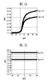
- FIGS. 3A is a graph showing drain currents ld(A), according to gate voltages Vg of a thin transistor, that does not include a passivation layer is not formed.
- FIG. 3B is a graph showing threshold voltages Vth over time, of the transistor.
- FIG. 4A is a graph showing a change of a drain currents ld(A), according to gate voltages Vg, of a thin transistor including a passivation layer 15 formed according to aspects of the present invention.
- FIG. 4B is a graph illustrating threshold voltages Vth according to stress time, of the transistor including the passivation layer 15. The measurement is performed for 50 hours, during which a voltage Vds of 10 V is applied to source and drain electrodes 16a and 16b.
- the gate voltage Vg is set to a current of 3 ⁇ A.
- the threshold voltage Vth abruptly increases in a positive (+) direction, as time elapses, and the threshold voltage increases such that it cannot be accurately measured after about 5 hours.
- the fluctuation width of the threshold voltage Vth is less than about 1V and remains stable for over 50 hours.
- a passivation layer is generally formed of a silicon oxide (SiO 2 ) silicon nitride (SiN x ), or aluminum oxide (Al 2 O 3 ).
- SiO 2 silicon oxide
- SiN x silicon nitride
- Al 2 O 3 aluminum oxide
- the electrical properties thereof can be seriously degraded. This degradation is inferred to be generated by plasma during a deposition process. If the damage occurs, the carrier concentration of the activation layer may increase, due to an oxygen deficiency. In addition, an off current may increase, due to the increased carrier concentration, resulting in a reduction in the S-factor thereof.
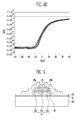
- FIG. 5A is a graph showing electrical properties of a thin film transistor, in which a passivation layer is not yet formed.
- FIG. 5B and 5C are graphs showing the electrical properties of a thin film transistor, in which a silicon oxide (SiO 2 ) passivation layer and an aluminum oxide (Al 2 O 3 ) passivation layer are formed, respectively.
- the passivation layers were formed using a conventional process. As shown in FIGS. 5B and 5C , after forming the silicon oxide (SiO 2 ) passivation layer and the aluminum oxide (Al 2 O 3 ) passivation layer, the electrical properties of the thin film transistors were reduced, as indicated by the I-V (current-voltage) curves.
- FIG. 6A shows results from a thin film transistor including a GalnZnO passivation layer and a GalnZnO activation layer.
- FIG. 6B shows results from a thin film transistor including a Ga 2 O 3 passivation layer and a GalnZnO activation layer.
- the threshold voltage increased by about 2.4V ( FIG. 6A ), and decreased by about 0.2V ( FIG. 6B ), as compared to the threshold voltage of 3.3V shown in FIG. 5A , when thin film transistor did not include the passivation layer.
- FIGS. 7A and 7B are graphs showing the reliability of a thin film transistor including an activation layer 14 formed by depositing GalnZnO at a pressure of 3mTorr, and a Ga 2 O 3 passivation layer, according to aspects of the present invention.
- the dashed lines represent a threshold voltage Vth, and the solid lines represent noise or abrupt voltage changes.
- the source and drain voltage was 10V, and the gate voltage was set to insure a constant current of 3 ⁇ A.
- FIG. 7A shows the change of the threshold voltage Vth
- FIG. 7B shows the change of the threshold voltage Vth
- the stable electrical properties are due to the passivation layer formed of an inorganic oxide.
- the passivation layer includes an inorganic oxide, the passivation layer 15 more easily captures (suppress) surplus carriers generated during a deposition process, thereby preventing the deterioration of electrical properties, due to the surplus carriers.
- the passivation layer of the present invention prevents the deterioration of transistor properties, due to external light.
- GalnZnO which is a compound semiconductor, has a band gap of 3.37eV, surplus carriers are generated if light is absorbed thereon, so that a leakage current may occur, and transistor properties may be degraded.
- a bottom gate structure is more susceptible to external light, as compared to a top gate structure.
- the passivation layer 15 is formed of silicon oxide (SiO 2 ), which has a larger band gap than GalnZnO, the external light is not blocked efficiently. Therefore, the transfer properties of the transistor deteriorated, as shown in FIG. 8A .
- FIG. 8A light of 0 to 20000 Lux was applied to the thin film transistor, when a 5.1V voltage Vds was applied to the source and drain electrodes 16a and 16b.
- the passivation layer is formed of an inorganic oxide, such as Ga 2 O 3 , which has a relatively small band gap equal or below 3.37eV or equal or below the GalnZnO band gap, so that the external light is absorbed with ease. Therefore, the activation layer was protected from the external light by the passivation layer, and detachment of oxygen due to the optical absorption of light are prevented, the transfer properties of the transistor were preserved, as shown in FIG. 8B .
- a conventional amorphous silicon thin film transistor generally has a dual gate structure, a lightly doped drain (LDD) structure, or an offset structure, which can reduce a leakage current.
- LDD lightly doped drain
- an offset structure which can reduce a leakage current.
- the passivation layer is formed of inorganic oxide having a band gap, but only a relatively small band gap, preferably equal or below 3.37eV, more preferably equal or below 3eV, external light is efficiently absorbed, so there is no need to add a separate process or device for compensating for the deterioration of the electrical properties.
- the band gap of the passivation layer 15 is not larger than the band gap of the activation layer 14.
- FIG. 9 is a cross-sectional view of a thin film transistor, according to another exemplary embodiment of the present invention. While the passivation layer 15 of the thin film transistor of FIG. 1 is formed across the activation layer 14 and the insulating film 13, the thin film transistor of FIG. 9 comprises a passivation layer 25 formed only on the activation layer. In addition, source and drain electrodes 26a and 26b contact source and drain regions 14b and 14c of the activation layer 14, without passing through contact holes in the passivation layer 15, as shown in FIG. 1 .
- the activation layer 14 can be protected by the passivation layer 25, and the contact resistance can also be reduced, by the direct contact of the source and drain electrodes 26a and 26b to the source and drain regions 14b and 14c.
- the passivation layer 25 can be formed of the same materials as the passivation layer 15.
- the thin film transistor of FIG. 9 can be manufactured using the same method as the thin film transistor of FIG. 1 , except that instead for forming the contact holes 15a by patterning the passivation layer 15, a portion of the passivation layer 25 is removed during patterning, such that the passivation layer 25 is only present on a portion of the activation layer 14.
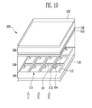
- FIG. 10 is a plan view of a flat panel display device including a thin film transistor, according to aspects of the present invention.
- the flat panel display device includes a display panel 100 that displays an image.
- the display panel 100 includes opposing first and second substrates 110 and 120, and a liquid crystal layer 130 disposed therebetween.
- a matrix of scan lines 111 and data lines 112 are disposed on the first substrate 110, and pixels 113 are formed in the matrix.
- Each pixel 113 includes a pixel electrode 115 and a thin film transistor 114.
- the thin film transistor 114 is connected to the scan lines 111 and the data lines 112.
- the thin film transistor 114 controls the supply of signals to each pixel electrode 115, from the scan lines 111 and data lines 111.
- the thin film transistor 114 can be exemplified by the thin film transistors of FIGS. 1 or 9 , and may be manufactured according to the manufacturing method of FIGS. 2A to 2D .
- a color filter 121 and a common electrode 122 are formed on an inner surface of the second substrate 120.
- Polarizing plates 116 and 123 are formed on outer surfaces of the first and second substrates 110 and 120, respectively.
- a backlight (not shown) can be disposed under the polarizing plate 116.
- a driver LCD Drive IC (not shown), which drives the display panel 100, is mounted in the periphery of the display panel 100. The driver converts externally supplied electrical signals into scan signals and data signals, which are supplied to the gate lines 111 and the data lines 112, respectively.
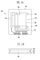
- FIGS. 11A and 11B are a plan view and a cross-sectional view of another exemplary embodiment of a flat panel display device.
- the flat panel display device includes a display panel 200 that displays an image.
- the display panel 200 includes a substrate 210 having a pixel region 220, and a non-pixel region 230 disposed around the pixel region 220.
- a plurality of organic light emitting devices 300 are disposed within, and connected to, a matrix of scan lines 224 and data lines 226, which are formed on the substrate 210.
- the scan lines 224 and data lines 226 extend into the pixel region 200.
- Power supply lines (not shown), which operate the organic light emitting device 300, and a scan driver 234 and a data driver 236, which supply signals to the scan lines 224 and the data lines 226, are formed in the non-pixel region 230.
- each organic light emitting device 300 includes an anode electrode 317, a cathode electrode 320, and an organic thin film layer 319 formed between the anode electrode 317 and the cathode electrode 320.
- the organic thin film layer 319 includes a hole transport layer, an organic light emitting layer, and an electron transport layer, which are stacked.
- the organic thin film layer 319 may also include a hole injection layer and an electron injection layer.
- the organic light emitting device 300 may further include thin film transistors which control the operation of the organic light emitting device 300, and a capacitor which maintains signals.
- the thin film transistor which can have the structures of FIGS. 1 or 9 , may be manufactured according to the exemplary manufacturing method of the present invention, as shown in FIGS. 2A to 2D .
- each organic light emitting device 300 a buffer layer 11 is formed on a substrate 210, and a gate electrode 12 is formed on the buffer layer 11, in a pixel region 220.
- the scan lines 224 are coupled to gate electrodes 12 of the organic light emitting devices 300 and to the scan driver 234.
- the data lines 226 connect the organic light emitting devices 300 to the data driver 236.
- Pads 228 to receive external signals may be formed in the non-pixel region 230.
- An activation layer 14 that includes a channel region, a source region, and a drain region, is formed on the gate electrode 12.
- the activation layer 14 is electrically insulated form the gate electrode 12, by a gate insulating film 13.
- a passivation layer 15 is formed on the activation layer 14, and contact holes are formed in the passivation layer 15, which expose the source and drain regions of the activation layer 14.
- the source and drain electrodes 16a and 16b are formed on the passivation layer 15 and are coupled to the source and drain regions 14b and 14c, through the contact holes.
- An organic planarization layer 17 is formed on the source and drain electrodes 16a and 16b.
- a hole is formed on the planarization layer 17, which exposes the drain electrode 16b.
- a pixel definition film 18 is formed on the planarization layer 17 and has a hole that exposes the anode electrode 317.
- An organic thin film layer 319 is formed on the exposed anode electrode 317, and a cathode electrode 320 is formed on the pixel defining film 318, in contact with the organic thin film layer 319.
- a sealing substrate 400 which seals the pixel regions 220, is disposed on the upper substrate 210.
- the sealing substrate 400 is bonded to the upper substrate 210 by a sealant 410, thereby completing a display panel 200.
Landscapes
- Physics & Mathematics (AREA)
- Nonlinear Science (AREA)
- Microelectronics & Electronic Packaging (AREA)
- Engineering & Computer Science (AREA)
- Mathematical Physics (AREA)
- Crystallography & Structural Chemistry (AREA)
- Chemical & Material Sciences (AREA)
- General Physics & Mathematics (AREA)
- Optics & Photonics (AREA)
- Geometry (AREA)
- Thin Film Transistor (AREA)
- Liquid Crystal (AREA)
- Electroluminescent Light Sources (AREA)
- Devices For Indicating Variable Information By Combining Individual Elements (AREA)
Abstract
Description
- Aspects of the present invention relate to a thin film transistor, a method of manufacturing the same, and a flat panel display device including the same.
- A thin film transistor generally includes: an activation layer including a channel region, a source region, and a drain region; and a gate electrode which is formed on the channel region. The gate electrode is electrically insulated from the activation layer, by a gate insulating film.
- An activation layer is generally formed of semiconductor material, such as amorphous silicon or poly-silicon. However, if an activation layer is formed of amorphous silicon, it is difficult to implement a high speed driving circuit, due to it having low electron mobility. If the activation layer is formed of poly-silicon, a separate compensation circuit should be added, due to uneven threshold voltages.
- A conventional method of manufacturing a thin film transistor, using a low temperature poly-silicon (LTPS), involves an expensive process such as a laser annealing. In addition, such a method is difficult to apply to larger substrates.
- Research into using a compound semiconductor as an activation layer has been recently conducted, in order to solve the above problems. For example, Japanese Patent Laid-Open Publication No.
2004-273614 - The compound semiconductor is evaluated as a stable material, having an amorphous shape. If such a compound semiconductor is used as an activation layer, the compound semiconductor has various advantages, in that the thin film transistor may be manufactured at a temperature below 350°C , using existing processing equipment. In addition, an ion implantation process may be omitted.
- However, a compound semiconductor can be damaged by plasma, when a thin film formed thereon is etched. Such damage degrades the electrical properties of the compound semiconductor, such that the threshold voltage of the thin film transistor changes.
- Aspects of the present invention provide a thin film transistor having improved damage resistance, during the formation and/or patterning of a passivation layer, a method of manufacturing the same, and a flat panel display device having the same.
- Aspects of the present invention provide a thin film transistor that resists damage due to external light, a method of manufacturing the same, and a flat panel display device having the same.
- Aspects of the present invention proved a thin film transistor, comprising: a substrate; a gate electrode formed on the substrate; a gate insulating film formed on the gate electrode; an activation layer formed on the gate insulating film, including a compound semiconductor oxide; a passivation layer formed on the activation layer; and source electrode and drain electrodes that contact the activation layer. The passivation layer is formed of an inorganic oxide.
- According to another aspect of the present invention, there is provided a method of manufacturing a thin film transistor, comprising: forming a gate electrode on a substrate; forming a gate insulating film on the gate electrode; forming an activation layer including a compound semiconductor oxide, on the gate insulating film; forming a passivation layer including an inorganic oxide, on the activation layer; and forming source and drain electrodes that contact the activation layer.
- According to another aspect of the present invention, there is provided a flat panel display device, comprising: opposing first and second substrates; pixel electrodes formed on the first substrate, scan and data lines formed around the pixel electrodes; thin film transistors connected to the pixel electrodes, the scan lines, and the data lines, which control signals supplied to each pixel electrode; and a liquid crystal injected into a sealed space between the first and second substrates. Each thin film transistor comprises: a gate electrode formed on the first substrate; an activation layer formed of a compound semiconductor oxide, which is insulated from the gate electrode by a gate insulating film; a passivation layer formed on the activation layer; and source electrode and drain electrode which contact the activation layer. The passivation layer is formed of an inorganic oxide.
- According to another aspect of the present invention, provided is a flat panel display device, comprising: opposing first and second substrates; organic light emitting devices formed on the first substrate; scan and data lines formed around the organic light emitting devices; and thin film transistors connected to the scan lines, the data lines, and the organic light emitting devices. Each organic light emitting device includes a first electrode, an organic thin film layer, and a second electrode. Each thin film transistor comprises: a gate electrode formed on the first substrate; an compound semiconductor oxide activation layer that is insulated from the gate electrode, by a gate insulating film; an inorganic oxide passivation layer formed on the activation layer; and source and drain electrodes that contact the activation layer.
- According to another aspect of the present invention, the passivation layer, can be used as an etch stop layer, during the formation of the source and drain electrodes, which prevents the channel region from being contaminated and/or damaged, even if the activation is damaged. The passivation layer enables the activation layer to be restored through a subsequent annealing process. Therefore, aspects of the present invention can prevent the deterioration of the electrical properties of the thin film transistor, due to the damaging of the activation layer, and can improve the properties of the substrate. The passivation layer is formed of an inorganic oxide having a relatively small band gap, making it possible to absorb external light efficiently.
- Additional aspects and/or advantages of the invention will be set forth in part in the description which follows and, in part, will be obvious from the description, or may be learned by practice of the invention.
- These and/or other aspects and advantages of the invention will become apparent and more readily appreciated from the following description of the embodiments, taken in conjunction with the accompanying drawings of which:
-
FIG. 1 is a cross-sectional view of a thin film transistor, according to aspects of the present invention; -
FIGS. 2A to 2D are cross-sectional views of a method of manufacturing a thin film transistor, according to an exemplary embodiment of the present invention; -
FIGS. 3A and4A are graphs showing drain currents according to gate voltages; -
FIGS. 3B and4B are graphs showing changes in threshold voltages, over time; -
FIG. 5A is a graph showing the electrical properties of a thin film transistor without a passivation layer; -
FIGS. 5B and5C are graphs showing the electrical properties of a thin film transistor with a passivation layer; -
FIGS. 6A and6B are graphs showing the electrical properties of thin film transistors, according to aspects of the present invention; -
FIGS. 7A and7B are graphs showing the reliability of a thin film transistor, according to aspects of the present invention; -
FIGS. 8A and8B are graphs showing the transfer properties of a transistor, according to the absorption of external light; -
FIG. 9 is a cross-sectional view of a thin film transistor, according to an exemplary embodiment of the present invention; -
FIG. 10 is a plan view of a flat panel display device having a thin film transistor, according to an exemplary embodiment the present invention; -
FIGS. 11A and 11 B are respectively a plan view and a cross-sectional view of a flat panel display device having a thin film transistor, according to an exemplary embodiment of the present invention; and -
FIG. 12 is a cross-sectional view of an organic light emitting device ofFIGS. 11A and 11B . - Reference will now be made in detail to the exemplary embodiments of the present invention, examples of which are illustrated in the accompanying drawings, wherein like reference numerals refer to the like elements throughout. The exemplary embodiments are described below, in order to explain the aspects of the present invention, by referring to the figures. The described exemplary embodiments may be modified in various different ways, without departing from the scope of the present invention. Accordingly, the drawings and description are to be regarded as illustrative in nature and not restrictive. In addition, when an element is referred to as being "on" another element, it can be directly on another element or can be indirectly on the element with one, or one or more intervening elements can be interposed therebetween. Also, when an element is referred to as being "connected to" another element, it can be directly connected to the element, or can be indirectly connected to the element, with one or more intervening elements interposed therebetween.
-
FIG. 1 is a cross-sectional view of a thin film transistor, according to an exemplary embodiment of the present invention. In the thin film transistor, abuffer layer 11 is formed on asubstrate 10, and agate electrode 12 is formed on thebuffer layer 11. Anactivation layer 14, which is insulated from thegate electrode 12 by agate insulating film 13, is formed on thegate insulating film 13, over thegate electrode 12. Theactivation layer 14 can be formed of a compound semiconductor oxide. Achannel region 14a, asource region 14b, and adrain region 14c are provided in theactivation layer 14. Thechannel region 14a overlaps thegate electrode 12. - A
passivation layer 15 is formed separately on theactivation layer 14 and the insulatingfilm 13. Contact holes are formed in thepassivation layer 15, which expose the source and drainregions drain electrodes regions - The
activation layer 14 may be formed of a compound semiconductor oxide or zinc oxide (ZnO). Herein, a compound semiconductor oxide refers to a semiconductor compound including elements from two or more different groups of the periodic table and oxygen. Theactivation layer 14 may be doped with at least one ion of gallium (Ga), indium (In), stannum (Sn), zirconium (Zr), hafnium (Hf), and vanadium (V). Thepassivation layer 15 is formed of an inorganic oxide. The inorganic oxide may include elements being selected from a group consisting of gallium (Ga), indium (In), stannum (Sn), zirconium (Zr), hafnium (Hf), and vanadium (V), or may include silicon (Si) or aluminum (AI). -
FIGS. 2A to 2D are cross-sectional views of a method of manufacturing a thin film transistor, according to an exemplary embodiment of the present invention. Referring toFIG. 2A , abuffer layer 11 is formed on asubstrate 10, and agate electrode 12 is formed on thebuffer layer 11. Agate insulating film 13 is formed on thegate electrode 12 and thebuffer layer 11. Thesubstrate 10 may be a semiconductor substrate such as silicon (Si); an insulating substrate, such as glass, or plastic; or a metal substrate. Thegate electrode 12 may include Al, Cr, or MoW, or may include a conductive polymer. Thegate insulating film 13 may be formed of an insulating material, such as SiO2 SiNx, or Ga2O3. - Referring to
FIG. 2B , theactivation layer 14 is formed on thegate insulating film 13, above thegate electrode 12. Theactivation layer 14 includes achannel region 14a, asource region 14b, and adrain region 14c. Theactivation layer 14 may be formed of the compound semiconductor oxide or zinc oxide. For example, theactivation layer 14 may be formed of or consist of ZnO, ZnGaO, ZnlnO, ZnSnO, or GalnZnO. - Referring to
FIG. 2C , apassivation layer 15 is then formed and patterned, thereby formingcontact holes 15a that expose the source and drainregions passivation layer 15 is formed of an inorganic oxide including, for example, elements being selected from a group consisting of gallium (Ga), indium (In), stannum (Sn), zirconium (Zr), hafnium (Hf), and vanadium (V), or may include silicon (Si) or aluminum (Al). Thepassivation layer 15 may be formed of the same material as the compound semiconductor oxide. For example, the passivation layer may be formed of or consists of ZnO, ZnGaO, ZnlnO, ZnSnO, GaO, HfO, or GaInZnO. Thepassivation layer 15 may alternatively include at least some elements included in the compound semiconductor oxide, such as Ga2O3. Thepassivation layer 15 may also include a silicon oxide (SiO2), aluminum oxide (Al2O3), or aluminum oxynitride (ALON). - When a silicon oxide is used, a deposition temperature is set to below 300°C, and an oxygen partial pressure is set to at least 50%. When the aluminum oxide is used, the deposition temperature is set to below 300°C, and the content of aluminum (AI) is set to from 2 to 50%. When the aluminum oxynitride is used, the oxygen partial pressure is set to about 4%, during a sputtering deposition process, using a target of aluminum oxide (Al2O3), in an atmosphere of nitrogen and argon.
- Referring to
FIG. 2D , after a conductive layer is formed on thepassivation layer 15 and in thecontact holes 15a, the conductive layer is patterned, thereby forming source anddrain electrodes regions contact holes 15a. The source anddrain electrodes - The
passivation layer 15 may be used as an etch stop layer, during the patterning of the conductive layer, which facilitates the etching process. Theactivation layer 14 is thereby protected in thechannel region 14a, during the etching process. Contamination of theactivation layer 14, due to organic material from a subsequent process, is also prevented. - However, when the
passivation layer 15 is formed of material having low etching selectivity, with respect to the compound semiconductor, theactivation layer 14 may be damaged during the etching of thecontact holes 15a. The material and/or the etching method should thus be selected accordingly. When theactivation layer 14 is damaged, theactivation layer 14 may be restored, however, if theactivation layer 14 is annealed at a temperature of from 200 to 350°C, in vacuum of about 10e-2, and in an atmosphere of nitrogen (N2) and oxygen (O2), after the source anddrain electrodes - A deterioration of the electrical properties of the compound semiconductor, due to plasma damage, is inferred to be primarily generated by an oxygen deficiency, resulting from the breakage of surface gratings. Therefore, aspects of the present invention protect the
activation layer 14, by using the inorganicoxide passivation layer 15. This also permits the restoration of theactivation layer 14, through the subsequent annealing. The restoration of theactivation layer 14 is inferred to result from oxygen diffusing from thepassivation layer 15. -
FIGS. 3A is a graph showing drain currents ld(A), according to gate voltages Vg of a thin transistor, that does not include a passivation layer is not formed.FIG. 3B is a graph showing threshold voltages Vth over time, of the transistor.FIG. 4A is a graph showing a change of a drain currents ld(A), according to gate voltages Vg, of a thin transistor including apassivation layer 15 formed according to aspects of the present invention.FIG. 4B is a graph illustrating threshold voltages Vth according to stress time, of the transistor including thepassivation layer 15. The measurement is performed for 50 hours, during which a voltage Vds of 10 V is applied to source anddrain electrodes - In the cases of
FIGS. 3A and 3B , the threshold voltage Vth abruptly increases in a positive (+) direction, as time elapses, and the threshold voltage increases such that it cannot be accurately measured after about 5 hours. On the contrary, in the cases ofFIGS. 4A and 4B , the fluctuation width of the threshold voltage Vth is less than about 1V and remains stable for over 50 hours. - In a conventional thin film transistor having a polysilicon activation layer, a passivation layer is generally formed of a silicon oxide (SiO2) silicon nitride (SiNx), or aluminum oxide (Al2O3). However, in the case of a thin film transistor having an activation layer formed of a compound semiconductor oxide, if a passivation layer is formed of a conventionally formed silicon oxide (SiO2), silicon nitride (SiNx), or aluminum oxide (Al2O3), the electrical properties thereof, can be seriously degraded. This degradation is inferred to be generated by plasma during a deposition process. If the damage occurs, the carrier concentration of the activation layer may increase, due to an oxygen deficiency. In addition, an off current may increase, due to the increased carrier concentration, resulting in a reduction in the S-factor thereof.
-
FIG. 5A is a graph showing electrical properties of a thin film transistor, in which a passivation layer is not yet formed.FIG. 5B and5C are graphs showing the electrical properties of a thin film transistor, in which a silicon oxide (SiO2) passivation layer and an aluminum oxide (Al2O3) passivation layer are formed, respectively. The passivation layers were formed using a conventional process. As shown inFIGS. 5B and5C , after forming the silicon oxide (SiO2) passivation layer and the aluminum oxide (Al2O3) passivation layer, the electrical properties of the thin film transistors were reduced, as indicated by the I-V (current-voltage) curves. -
FIG. 6A shows results from a thin film transistor including a GalnZnO passivation layer and a GalnZnO activation layer.FIG. 6B shows results from a thin film transistor including a Ga2O3 passivation layer and a GalnZnO activation layer. The threshold voltage increased by about 2.4V (FIG. 6A ), and decreased by about 0.2V (FIG. 6B ), as compared to the threshold voltage of 3.3V shown inFIG. 5A , when thin film transistor did not include the passivation layer. -
FIGS. 7A and7B are graphs showing the reliability of a thin film transistor including anactivation layer 14 formed by depositing GalnZnO at a pressure of 3mTorr, and a Ga2O3 passivation layer, according to aspects of the present invention. InFIGS. 7A and7B , the dashed lines represent a threshold voltage Vth, and the solid lines represent noise or abrupt voltage changes. The source and drain voltage was 10V, and the gate voltage was set to insure a constant current of 3 µA. - There was slight changes in both cases when the measurements were taken after 50 hours (
FIG. 7A ) and after 10000 hours (FIG. 7B ). From the dashed line ofFIG. 7 , which shows the change of the threshold voltage Vth, it is inferred that there may be a change of 1.2V or less, after 30000 hours. - The stable electrical properties are due to the passivation layer formed of an inorganic oxide. In other words, since the passivation layer includes an inorganic oxide, the
passivation layer 15 more easily captures (suppress) surplus carriers generated during a deposition process, thereby preventing the deterioration of electrical properties, due to the surplus carriers. - Also, the passivation layer of the present invention prevents the deterioration of transistor properties, due to external light. Although GalnZnO, which is a compound semiconductor, has a band gap of 3.37eV, surplus carriers are generated if light is absorbed thereon, so that a leakage current may occur, and transistor properties may be degraded. In particular, a bottom gate structure is more susceptible to external light, as compared to a top gate structure.
- As shown in
FIG. 5B , if thepassivation layer 15 is formed of silicon oxide (SiO2), which has a larger band gap than GalnZnO, the external light is not blocked efficiently. Therefore, the transfer properties of the transistor deteriorated, as shown inFIG. 8A . InFIG. 8A , light of 0 to 20000 Lux was applied to the thin film transistor, when a 5.1V voltage Vds was applied to the source anddrain electrodes - However, in the thin film transistor of the present invention, as shown in
FIG. 6B , the passivation layer is formed of an inorganic oxide, such as Ga2O3, which has a relatively small band gap equal or below 3.37eV or equal or below the GalnZnO band gap, so that the external light is absorbed with ease. Therefore, the activation layer was protected from the external light by the passivation layer, and detachment of oxygen due to the optical absorption of light are prevented, the transfer properties of the transistor were preserved, as shown inFIG. 8B . - The deterioration of the activation layer, due to the absorption of light may cause a deterioration of image quality and an increase of power consumption of a display device including the thin film transistor. Therefore, a conventional amorphous silicon thin film transistor generally has a dual gate structure, a lightly doped drain (LDD) structure, or an offset structure, which can reduce a leakage current. However, in this case, there are problems that the drain current in a turned-on state is reduced, and additional processes are added. However, with the present invention, since the passivation layer is formed of inorganic oxide having a band gap, but only a relatively small band gap, preferably equal or below 3.37eV, more preferably equal or below 3eV, external light is efficiently absorbed, so there is no need to add a separate process or device for compensating for the deterioration of the electrical properties.
- Preferably, the band gap of the
passivation layer 15 is not larger than the band gap of theactivation layer 14. -
FIG. 9 is a cross-sectional view of a thin film transistor, according to another exemplary embodiment of the present invention. While thepassivation layer 15 of the thin film transistor ofFIG. 1 is formed across theactivation layer 14 and the insulatingfilm 13, the thin film transistor ofFIG. 9 comprises apassivation layer 25 formed only on the activation layer. In addition, source anddrain electrodes regions activation layer 14, without passing through contact holes in thepassivation layer 15, as shown inFIG. 1 . - The
activation layer 14 can be protected by thepassivation layer 25, and the contact resistance can also be reduced, by the direct contact of the source anddrain electrodes regions passivation layer 25 can be formed of the same materials as thepassivation layer 15. - The thin film transistor of
FIG. 9 can be manufactured using the same method as the thin film transistor ofFIG. 1 , except that instead for forming thecontact holes 15a by patterning thepassivation layer 15, a portion of thepassivation layer 25 is removed during patterning, such that thepassivation layer 25 is only present on a portion of theactivation layer 14. - The thin film transistors, according to aspects of the present invention, may be applied to a flat panel display device.
FIG. 10 is a plan view of a flat panel display device including a thin film transistor, according to aspects of the present invention. The flat panel display device includes adisplay panel 100 that displays an image. Thedisplay panel 100 includes opposing first andsecond substrates liquid crystal layer 130 disposed therebetween. A matrix ofscan lines 111 anddata lines 112 are disposed on thefirst substrate 110, andpixels 113 are formed in the matrix. - Each
pixel 113 includes apixel electrode 115 and athin film transistor 114. Thethin film transistor 114 is connected to thescan lines 111 and the data lines 112. Thethin film transistor 114 controls the supply of signals to eachpixel electrode 115, from thescan lines 111 anddata lines 111. Thethin film transistor 114, can be exemplified by the thin film transistors ofFIGS. 1 or9 , and may be manufactured according to the manufacturing method ofFIGS. 2A to 2D . - A
color filter 121 and acommon electrode 122 are formed on an inner surface of thesecond substrate 120. Polarizingplates second substrates polarizing plate 116. A driver LCD Drive IC (not shown), which drives thedisplay panel 100, is mounted in the periphery of thedisplay panel 100. The driver converts externally supplied electrical signals into scan signals and data signals, which are supplied to thegate lines 111 and thedata lines 112, respectively. -
FIGS. 11A and 11B are a plan view and a cross-sectional view of another exemplary embodiment of a flat panel display device. The flat panel display device includes adisplay panel 200 that displays an image. Thedisplay panel 200 includes asubstrate 210 having apixel region 220, and anon-pixel region 230 disposed around thepixel region 220. A plurality of organiclight emitting devices 300 are disposed within, and connected to, a matrix ofscan lines 224 anddata lines 226, which are formed on thesubstrate 210. Thescan lines 224 anddata lines 226 extend into thepixel region 200. Power supply lines (not shown), which operate the organiclight emitting device 300, and ascan driver 234 and adata driver 236, which supply signals to thescan lines 224 and thedata lines 226, are formed in thenon-pixel region 230. - Referring to
FIG. 12 , each organiclight emitting device 300 includes ananode electrode 317, acathode electrode 320, and an organicthin film layer 319 formed between theanode electrode 317 and thecathode electrode 320. The organicthin film layer 319 includes a hole transport layer, an organic light emitting layer, and an electron transport layer, which are stacked. The organicthin film layer 319 may also include a hole injection layer and an electron injection layer. The organiclight emitting device 300 may further include thin film transistors which control the operation of the organiclight emitting device 300, and a capacitor which maintains signals. The thin film transistor, which can have the structures ofFIGS. 1 or9 , may be manufactured according to the exemplary manufacturing method of the present invention, as shown inFIGS. 2A to 2D . - Referring to
FIGS. 11A and12 , in each organic light emitting device 300 abuffer layer 11 is formed on asubstrate 210, and agate electrode 12 is formed on thebuffer layer 11, in apixel region 220. Thescan lines 224 are coupled togate electrodes 12 of the organiclight emitting devices 300 and to thescan driver 234. The data lines 226 connect the organiclight emitting devices 300 to thedata driver 236.Pads 228 to receive external signals may be formed in thenon-pixel region 230. Anactivation layer 14 that includes a channel region, a source region, and a drain region, is formed on thegate electrode 12. Theactivation layer 14 is electrically insulated form thegate electrode 12, by agate insulating film 13. - A
passivation layer 15 is formed on theactivation layer 14, and contact holes are formed in thepassivation layer 15, which expose the source and drain regions of theactivation layer 14. The source anddrain electrodes passivation layer 15 and are coupled to the source and drainregions - An
organic planarization layer 17 is formed on the source anddrain electrodes planarization layer 17, which exposes thedrain electrode 16b. Ananode electrode 317 coupled to thedrain electrode 16b, via the hole. A pixel definition film 18 is formed on theplanarization layer 17 and has a hole that exposes theanode electrode 317. An organicthin film layer 319 is formed on the exposedanode electrode 317, and acathode electrode 320 is formed on thepixel defining film 318, in contact with the organicthin film layer 319. - Referring to
FIG. 11B , a sealingsubstrate 400, which seals thepixel regions 220, is disposed on theupper substrate 210. The sealingsubstrate 400 is bonded to theupper substrate 210 by asealant 410, thereby completing adisplay panel 200. - Although a few exemplary embodiments of the present invention have been shown and described, it would be appreciated by those skilled in the art that changes may be made in these exemplary embodiments, without departing from the scope of the invention as defined in the claims and their equivalents.
Claims (22)
- A thin film transistor, comprising:a substrate (10);a gate electrode (12) formed on the substrate (10);a gate insulating film (13) formed on the gate electrode (12) and the substrate (10);an activation layer (14) formed on the gate insulating film (13) and insulated from the gate electrode (12) by the gate insulating film (13);a passivation layer (15) formed on the activation layer (14); andsource and drain electrodes (16a, 16b) that contact the activation layer (14),characterized in that
the activation layer (14) comprises a compound semiconductor oxide or zinc oxide (Zn0), and
the passivation layer comprises an inorganic oxide. - The thin film transistor as claimed in claim 1, wherein the source and drain electrodes contact the activation layer (14), through contact holes formed in the passivation layer (15).
- The thin film transistor as claimed in claims 1 or 2, wherein the compound semiconductor oxide comprises or consists of zinc oxide (ZnO).
- The thin film transistor as claimed in one of the previous claims, wherein the compound semiconductor oxide is doped with at least one ion of gallium (Ga), indium (In), stannum (Sn), zirconium (Zr), hafnium (Hf), and vanadium (V).
- The thin film transistor as claimed in one of the previous claims, wherein the inorganic oxide comprises elements that are also comprised in the compound semiconductor oxide.
- The thin film transistor as claimed in claim 5, wherein the compound semiconductor oxide comprises gallium (Ga), indium (In), stannum (Sn), zirconium (Zr), hafnium (Hf), vanadium (V), or a combination thereof.
- The thin film transistor as claimed in claim 1, wherein the inorganic oxide comprises silicon (Si), aluminum (AI), silicon oxide (SiO2), aluminum oxide (Al2O3), gallium oxide (GaO), hafnium oxide (HfO), or aluminum oxynitride (ALON).
- The thin film transistor as claimed in one of the previous claims, further comprising a buffer layer (11) formed between the substrate (10) and the gate electrode (12).
- The thin film transistor of one of the previous claims, wherein the band gap of the passivation layer (15) is not larger than the band gap of the activation layer (14).
- A method of manufacturing a thin film transistor, comprising:forming a gate electrode (12) on a substrate (10);forming a gate insulating film (13) on the gate electrode (12);forming an activation layer (14) comprising a compound semiconductor oxide or zinc oxide (ZnO), on the gate insulating film (13);forming a passivation layer (15) comprising an inorganic oxide, on the activation layer (14); andforming source and drain electrodes (16a, 16b) in contact with the activation layer (14).
- The method of manufacturing the thin film transistor as claimed in claim 10, wherein the forming of the passivation layer (15) comprises: forming contact holes in the passivation layer (15).
- The method of manufacturing the thin film transistor as claimed in claims 10 or 11, wherein the forming of the source and drain electrodes comprises:forming a conductive layer (16) on the passivation layer (15) and in the contact holes; andpatterning the conductive layer (16) to form the source and drain electrodes (16a, 16b), which contact the activation layer (14) through the contact holes.
- The method of manufacturing the thin film transistor as claimed in one of the previous method claims, further comprising annealing the passivation layer (15).
- The method of manufacturing the thin film transistor as claimed in one of the previous method claims, wherein the activation layer (14) comprises zinc oxide (ZnO).
- The method of manufacturing the thin film transistor as claimed in one of the previous method claims, wherein the compound semiconductor oxide is doped with at least one ion of gallium (Ga), indium (In), stannum (Sn), zirconium (Zr), hafnium (Hf), and vanadium (V).
- The method of manufacturing the thin film transistor as claimed in one of the previous method claims, wherein the inorganic oxide comprises elements that are also comprised in the compound semiconductor oxide.
- The method of manufacturing the thin film transistor as claimed in claim 16, wherein the compound semiconductor oxide comprises gallium (Ga), indium (In), stannum (Sn), zirconium (Zr), hafnium (Hf), vanadium (V), or a combination thereof.
- The method of manufacturing the thin film transistor as claimed in claim 10, wherein the inorganic oxide comprises silicon (Si) or aluminum (AI).
- The method of manufacturing the thin film transistor as claimed in one of the previous method claims, wherein the forming of the source and drain electrodes comprises using the passivation layer (15) as an etch stop layer.
- The method of manufacturing the thin film transistor as claimed in claim 10, further comprising forming a buffer layer (11) on the substrate (10).
- A flat panel display device, comprising:opposing first and second substrates (110, 120);pixel electrodes (115) disposed on the first substrate (110)scan and data lines (111, 112) disposed on the first substrate (110), around the pixel electrodes (115);thin film transistors (114) according to one of the claims 1-9 connected to the scan lines (111), the data lines (112), and the pixel electrodes (115), to control the operations of the pixel electrodes (115),a common electrode (122) disposed on the second substrate (120); anda liquid crystal layer (130) injected into a space between the first and second substrates (110, 120).
- Aflat panel display device, comprising:opposing first and second substrates (210, 400);organic light emitting devices (300) disposed on the first substrate (210);scan and data lines (224, 226) disposed on the first substrate (210), around the organic light emitting devices (300);thin film transistors according to one of the claims 1-9 connected to the scan lines (224), the data lines (226), and the organic light emitting devices (300), to control the operation of the organic light emitting devices (300).
Applications Claiming Priority (1)
| Application Number | Priority Date | Filing Date | Title |
|---|---|---|---|
| KR1020080066002A KR100963104B1 (en) | 2008-07-08 | 2008-07-08 | Thin film transistor, its manufacturing method, and flat panel display device comprising thin film transistor |
Publications (2)
| Publication Number | Publication Date |
|---|---|
| EP2144294A1 true EP2144294A1 (en) | 2010-01-13 |
| EP2144294B1 EP2144294B1 (en) | 2018-11-21 |
Family
ID=41211906
Family Applications (1)
| Application Number | Title | Priority Date | Filing Date |
|---|---|---|---|
| EP09164894.9A Active EP2144294B1 (en) | 2008-07-08 | 2009-07-08 | Method of manufacturing thin film transistor and flat panel display device having the same |
Country Status (5)
| Country | Link |
|---|---|
| US (3) | US8178884B2 (en) |
| EP (1) | EP2144294B1 (en) |
| JP (1) | JP5542352B2 (en) |
| KR (1) | KR100963104B1 (en) |
| CN (1) | CN101626036B (en) |
Cited By (19)
| Publication number | Priority date | Publication date | Assignee | Title |
|---|---|---|---|---|
| WO2011118741A1 (en) * | 2010-03-26 | 2011-09-29 | Semiconductor Energy Laboratory Co., Ltd. | Method for manufacturing semiconductor device |
| US8546180B2 (en) | 2009-07-31 | 2013-10-01 | Semiconductor Energy Laboratory Co., Ltd. | Method for manufacturing oxide semiconductor device |
| US8704219B2 (en) | 2010-03-26 | 2014-04-22 | Semiconductor Energy Laboratory Co., Ltd. | Method for manufacturing semiconductor device |
| US9373707B2 (en) | 2010-04-23 | 2016-06-21 | Semiconductor Energy Laboratory Co., Ltd. | Manufacturing method of semiconductor device with steps of heat treatment in nitrogen containing atmosphere, oxygen doping treatment and heat treatment in oxygen containing atmosphere |
| US9576982B2 (en) | 2011-11-11 | 2017-02-21 | Semiconductor Energy Laboratory Co., Ltd. | Liquid crystal display device, EL display device, and manufacturing method thereof |
| US9673305B2 (en) | 2010-11-11 | 2017-06-06 | Semiconductor Energy Laboratory Co., Ltd. | Semiconductor device and method for manufacturing the same |
| US9698008B2 (en) | 2010-04-16 | 2017-07-04 | Semiconductor Energy Laboratory Co., Ltd. | Deposition method and method for manufacturing semiconductor device |
| US9755082B2 (en) | 2010-06-11 | 2017-09-05 | Semiconductor Energy Laboratory Co., Ltd. | Semiconductor device including oxide semiconductor with an insulating film including galliium and oxygen |
| US9812560B2 (en) | 2010-06-01 | 2017-11-07 | Semiconductor Energy Laboratory Co., Ltd. | Field effect transistor and method for manufacturing the same |
| US9882062B2 (en) | 2011-01-12 | 2018-01-30 | Semiconductor Energy Laboratory Co., Ltd. | Semiconductor device and manufacturing method thereof |
| US9917204B2 (en) | 2011-03-31 | 2018-03-13 | Semiconductor Energy Laboratory Co., Ltd. | Semiconductor device |
| US9954007B2 (en) | 2009-09-04 | 2018-04-24 | Semiconductor Energy Laboratory Co., Ltd. | Transistor and display device |
| US9954084B2 (en) | 2010-03-26 | 2018-04-24 | Semiconductor Energy Laboratory Co., Ltd. | Method for manufacturing semiconductor device |
| US9978878B2 (en) | 2010-04-23 | 2018-05-22 | Semiconductor Energy Laboratory Co., Ltd. | Manufacturing method of semiconductor device |
| US10008515B2 (en) | 2010-04-09 | 2018-06-26 | Semiconductor Energy Laboratory Co., Ltd. | Semiconductor device |
| US10043918B2 (en) | 2011-07-08 | 2018-08-07 | Semiconductor Energy Laboratory Co., Ltd. | Semiconductor device and manufacturing method thereof |
| US10158026B2 (en) | 2012-04-13 | 2018-12-18 | Semiconductor Energy Laboratory Co., Ltd. | Semiconductor device including oxide semiconductor stacked layers |
| US10304859B2 (en) | 2013-04-12 | 2019-05-28 | Semiconductor Energy Laboratory Co., Ltd. | Semiconductor device having an oxide film on an oxide semiconductor film |
| US10608116B2 (en) | 2010-04-02 | 2020-03-31 | Semiconductor Energy Laboratory Co., Ltd. | Semiconductor device |
Families Citing this family (97)
| Publication number | Priority date | Publication date | Assignee | Title |
|---|---|---|---|---|
| JP2010205987A (en) * | 2009-03-04 | 2010-09-16 | Sony Corp | Thin film transistor, method for manufacturing the same, and display |
| WO2011001880A1 (en) | 2009-06-30 | 2011-01-06 | Semiconductor Energy Laboratory Co., Ltd. | Method for manufacturing semiconductor device |
| CN111081550A (en) | 2009-06-30 | 2020-04-28 | 株式会社半导体能源研究所 | Method for manufacturing semiconductor device and semiconductor device |
| KR101457837B1 (en) | 2009-06-30 | 2014-11-05 | 가부시키가이샤 한도오따이 에네루기 켄큐쇼 | Method for manufacturing semiconductor device |
| WO2011013523A1 (en) | 2009-07-31 | 2011-02-03 | Semiconductor Energy Laboratory Co., Ltd. | Semiconductor device and method for manufacturing the same |
| CN102473734B (en) | 2009-07-31 | 2015-08-12 | 株式会社半导体能源研究所 | Semiconductor device and manufacturing method thereof |
| WO2011013502A1 (en) | 2009-07-31 | 2011-02-03 | Semiconductor Energy Laboratory Co., Ltd. | Semiconductor device and manufacturing method thereof |
| KR20120051727A (en) | 2009-07-31 | 2012-05-22 | 가부시키가이샤 한도오따이 에네루기 켄큐쇼 | Semiconductor device and manufacturing method thereof |
| KR101073543B1 (en) * | 2009-09-04 | 2011-10-17 | 삼성모바일디스플레이주식회사 | Organic light emitting display |
| KR101470811B1 (en) * | 2009-09-16 | 2014-12-09 | 가부시키가이샤 한도오따이 에네루기 켄큐쇼 | Semiconductor device |
| KR101147414B1 (en) * | 2009-09-22 | 2012-05-22 | 삼성모바일디스플레이주식회사 | Organic light emitting diode display and method for manufacturing the same |
| WO2011062043A1 (en) | 2009-11-20 | 2011-05-26 | Semiconductor Energy Laboratory Co., Ltd. | Method for manufacturing semiconductor device |
| KR102450889B1 (en) | 2009-12-04 | 2022-10-06 | 가부시키가이샤 한도오따이 에네루기 켄큐쇼 | Semiconductor device |
| KR101649732B1 (en) * | 2009-12-10 | 2016-08-22 | 삼성디스플레이 주식회사 | Thin film transistor array panel and manufacturing method thereof |
| KR20110093113A (en) | 2010-02-11 | 2011-08-18 | 삼성전자주식회사 | Thin film transistor substrate and manufacturing method thereof |
| KR101084192B1 (en) | 2010-02-16 | 2011-11-17 | 삼성모바일디스플레이주식회사 | Organic light emitting display |
| CN102782859B (en) * | 2010-02-26 | 2015-07-29 | 株式会社半导体能源研究所 | The manufacture method of semiconductor device |
| JP5731244B2 (en) * | 2010-03-26 | 2015-06-10 | 株式会社半導体エネルギー研究所 | Method for manufacturing semiconductor device |
| US9196739B2 (en) * | 2010-04-02 | 2015-11-24 | Semiconductor Energy Laboratory Co., Ltd. | Semiconductor device including oxide semiconductor film and metal oxide film |
| KR101977152B1 (en) | 2010-04-02 | 2019-05-10 | 가부시키가이샤 한도오따이 에네루기 켄큐쇼 | Semiconductor device |
| US9190522B2 (en) | 2010-04-02 | 2015-11-17 | Semiconductor Energy Laboratory Co., Ltd. | Semiconductor device having an oxide semiconductor |
| US8884282B2 (en) | 2010-04-02 | 2014-11-11 | Semiconductor Energy Laboratory Co., Ltd. | Semiconductor device |
| US9147768B2 (en) | 2010-04-02 | 2015-09-29 | Semiconductor Energy Laboratory Co., Ltd. | Semiconductor device having an oxide semiconductor and a metal oxide film |
| KR20110114089A (en) | 2010-04-12 | 2011-10-19 | 삼성모바일디스플레이주식회사 | Thin film transistor, method for manufacturing same and display device including same |
| WO2011132591A1 (en) | 2010-04-23 | 2011-10-27 | Semiconductor Energy Laboratory Co., Ltd. | Method for manufacturing semiconductor device |
| WO2011132556A1 (en) | 2010-04-23 | 2011-10-27 | Semiconductor Energy Laboratory Co., Ltd. | Method for manufacturing semiconductor device |
| CN111326435B (en) | 2010-04-23 | 2023-12-01 | 株式会社半导体能源研究所 | Semiconductor device manufacturing method |
| KR101689378B1 (en) | 2010-04-23 | 2016-12-26 | 가부시키가이샤 한도오따이 에네루기 켄큐쇼 | Method for manufacturing semiconductor device |
| WO2011135987A1 (en) | 2010-04-28 | 2011-11-03 | Semiconductor Energy Laboratory Co., Ltd. | Method for manufacturing semiconductor device |
| KR101806271B1 (en) | 2010-05-14 | 2017-12-07 | 가부시키가이샤 한도오따이 에네루기 켄큐쇼 | Method for manufacturing semiconductor device |
| WO2011145468A1 (en) | 2010-05-21 | 2011-11-24 | Semiconductor Energy Laboratory Co., Ltd. | Memory device and semiconductor device |
| US8629438B2 (en) | 2010-05-21 | 2014-01-14 | Semiconductor Energy Laboratory Co., Ltd. | Semiconductor device and manufacturing method thereof |
| KR101862808B1 (en) * | 2010-06-18 | 2018-05-30 | 가부시키가이샤 한도오따이 에네루기 켄큐쇼 | Semiconductor device |
| WO2011158704A1 (en) | 2010-06-18 | 2011-12-22 | Semiconductor Energy Laboratory Co., Ltd. | Method for manufacturing semiconductor device |
| CN107195686B (en) * | 2010-07-02 | 2021-02-09 | 株式会社半导体能源研究所 | Semiconductor device with a plurality of semiconductor chips |
| JP2012028481A (en) * | 2010-07-22 | 2012-02-09 | Fujifilm Corp | Field-effect transistor and manufacturing method of the same |
| US8450123B2 (en) * | 2010-08-27 | 2013-05-28 | Semiconductor Energy Laboratory Co., Ltd. | Oxygen diffusion evaluation method of oxide film stacked body |
| KR101789236B1 (en) | 2010-12-24 | 2017-10-24 | 삼성디스플레이 주식회사 | Thin film transistor and flat display device |
| CN102157563B (en) * | 2011-01-18 | 2012-09-19 | 上海交通大学 | Metal Oxide Thin Film Transistor Fabrication Method |
| TWI624878B (en) | 2011-03-11 | 2018-05-21 | 半導體能源研究所股份有限公司 | Semiconductor device manufacturing method |
| KR101781532B1 (en) * | 2011-03-14 | 2017-10-24 | 삼성디스플레이 주식회사 | An organic light emitting display device and the manufacturing method thereof |
| US9634029B2 (en) | 2011-03-17 | 2017-04-25 | E Ink Holdings Inc. | Thin film transistor substrate and display device having same |
| TWI451573B (en) * | 2011-03-17 | 2014-09-01 | E Ink Holdings Inc | Display device and thin film transistor structure thereof |
| CN102208441A (en) * | 2011-05-03 | 2011-10-05 | 复旦大学 | Film transistor active layer and growth method thereof |
| US8709922B2 (en) * | 2011-05-06 | 2014-04-29 | Semiconductor Energy Laboratory Co., Ltd. | Semiconductor device |
| TWI557910B (en) * | 2011-06-16 | 2016-11-11 | 半導體能源研究所股份有限公司 | Semiconductor device and method of manufacturing same |
| US9385238B2 (en) | 2011-07-08 | 2016-07-05 | Semiconductor Energy Laboratory Co., Ltd. | Transistor using oxide semiconductor |
| KR101239231B1 (en) | 2011-07-22 | 2013-03-11 | 한국과학기술연구원 | Thin film transistor having passivation layer comprising metal and method for fabricating the same |
| KR102029389B1 (en) * | 2011-09-02 | 2019-11-08 | 엘지디스플레이 주식회사 | Flat panel display device with oxide thin film transistor and method for fabricating the same |
| KR101506303B1 (en) * | 2011-09-29 | 2015-03-26 | 가부시키가이샤 한도오따이 에네루기 켄큐쇼 | Semiconductor device and method for manufacturing the same |
| US9018629B2 (en) | 2011-10-13 | 2015-04-28 | Semiconductor Energy Laboratory Co., Ltd. | Semiconductor device and method for manufacturing semiconductor device |
| JP6226518B2 (en) * | 2011-10-24 | 2017-11-08 | 株式会社半導体エネルギー研究所 | Semiconductor device |
| KR20130049620A (en) * | 2011-11-04 | 2013-05-14 | 삼성디스플레이 주식회사 | Display device |
| JP6122275B2 (en) | 2011-11-11 | 2017-04-26 | 株式会社半導体エネルギー研究所 | Display device |
| US9082861B2 (en) * | 2011-11-11 | 2015-07-14 | Semiconductor Energy Laboratory Co., Ltd. | Transistor with oxide semiconductor channel having protective layer |
| JP2013115098A (en) * | 2011-11-25 | 2013-06-10 | Sony Corp | Transistor, transistor manufacturing method, display device and electronic apparatus |
| KR102100425B1 (en) | 2011-12-27 | 2020-04-13 | 가부시키가이샤 한도오따이 에네루기 켄큐쇼 | Semiconductor device and method for manufacturing the same |
| CN102651401B (en) | 2011-12-31 | 2015-03-18 | 京东方科技集团股份有限公司 | A kind of thin film transistor, array substrate and its manufacturing method and display device |
| CN102751240B (en) | 2012-05-18 | 2015-03-11 | 京东方科技集团股份有限公司 | Thin film transistor array substrate, manufacturing method thereof, display panel and display device |
| CN102723344B (en) * | 2012-06-12 | 2015-07-15 | 南京中电熊猫液晶显示科技有限公司 | Array substrate, manufacture method of array substrate and liquid crystal display |
| CN103578984B (en) * | 2012-07-26 | 2016-10-26 | 瀚宇彩晶股份有限公司 | Semiconductor element and its manufacturing method |
| US8653516B1 (en) * | 2012-08-31 | 2014-02-18 | Eastman Kodak Company | High performance thin film transistor |
| CN102800709B (en) | 2012-09-11 | 2015-07-01 | 深圳市华星光电技术有限公司 | Driving device for thin film transistor |
| TWI671910B (en) | 2012-09-24 | 2019-09-11 | 日商半導體能源研究所股份有限公司 | Semiconductor device |
| CN102916051B (en) * | 2012-10-11 | 2015-09-02 | 京东方科技集团股份有限公司 | A kind of thin-film transistor and preparation method thereof, array base palte and display unit |
| CN102955312B (en) * | 2012-11-14 | 2015-05-20 | 京东方科技集团股份有限公司 | Array substrate and manufacture method thereof and display device |
| KR102495290B1 (en) | 2012-12-28 | 2023-02-06 | 가부시키가이샤 한도오따이 에네루기 켄큐쇼 | Semiconductor device |
| JP5960626B2 (en) * | 2013-03-08 | 2016-08-02 | 富士フイルム株式会社 | Manufacturing method of semiconductor device provided with thin film transistor |
| WO2014181777A1 (en) | 2013-05-09 | 2014-11-13 | 独立行政法人物質・材料研究機構 | Thin-film transistor and method for manufacturing same |
| KR101498522B1 (en) * | 2013-07-17 | 2015-03-04 | 한국광기술원 | Fabrication method of high quality oxide thin films for micribolometer |
| KR102130139B1 (en) | 2013-07-30 | 2020-07-03 | 엘지디스플레이 주식회사 | Organic Light Emitting Diode Display Having Thin Film Transistor Substrate Using Oxide Semiconductor And Method For Manufacturing The Same |
| KR20150030034A (en) * | 2013-09-11 | 2015-03-19 | 삼성디스플레이 주식회사 | display apparatus and manufacturing method for the same |
| TWI677989B (en) | 2013-09-19 | 2019-11-21 | 日商半導體能源研究所股份有限公司 | Semiconductor device and manufacturing method thereof |
| DE102013111501B4 (en) | 2013-10-18 | 2024-02-08 | Universität Stuttgart | Thin film transistor and process for its production |
| US9590111B2 (en) * | 2013-11-06 | 2017-03-07 | Semiconductor Energy Laboratory Co., Ltd. | Semiconductor device and display device including the semiconductor device |
| JP6496132B2 (en) * | 2013-12-02 | 2019-04-03 | 株式会社半導体エネルギー研究所 | Semiconductor device |
| TWI721409B (en) | 2013-12-19 | 2021-03-11 | 日商半導體能源研究所股份有限公司 | Semiconductor device |
| KR102172972B1 (en) * | 2014-02-26 | 2020-11-03 | 삼성디스플레이 주식회사 | Thin film transistor and method for fabricating the same |
| KR102449437B1 (en) | 2014-06-26 | 2022-09-30 | 인텔 코포레이션 | Non-planar semiconductor device having omega fins with doped lower fin regions and method of manufacturing same |
| CN104091809B (en) * | 2014-06-26 | 2017-01-25 | 京东方科技集团股份有限公司 | Array substrate, preparation method of array substrate, LCD and display device |
| CN104538400B (en) * | 2014-12-16 | 2017-08-04 | 深圳市华星光电技术有限公司 | A kind of LTPS array substrate |
| CN104900711B (en) * | 2015-06-08 | 2019-11-05 | 京东方科技集团股份有限公司 | Thin film transistor and its manufacturing method and array substrate, display device |
| TWI650817B (en) | 2015-08-28 | 2019-02-11 | 聯華電子股份有限公司 | Semiconductor structure and method of forming the same |
| KR20170027932A (en) * | 2015-09-02 | 2017-03-13 | 삼성디스플레이 주식회사 | Thin film transistor array panel and method of manufacturing the same |
| KR102483953B1 (en) * | 2015-10-16 | 2023-01-03 | 삼성디스플레이 주식회사 | Thin film Transistor substrate and organic light emitting display using the same |
| CN105633170A (en) * | 2016-02-23 | 2016-06-01 | 广州新视界光电科技有限公司 | Metal oxide thin film transistor and preparation method therefor, array substrate and display apparatus |
| CN105742297B (en) * | 2016-04-13 | 2019-09-24 | 深圳市华星光电技术有限公司 | Thin-film transistor display panel and preparation method thereof |
| US20190140102A1 (en) * | 2016-04-25 | 2019-05-09 | Sakai Display Products Corporation | Thin film transistor, display device, and thin film transistor manufacturing method |
| KR102660292B1 (en) * | 2016-06-23 | 2024-04-24 | 삼성디스플레이 주식회사 | Thin film transistor array panel and manufacturing method thereof |
| CN106252362B (en) * | 2016-08-31 | 2019-07-12 | 深圳市华星光电技术有限公司 | A kind of array substrate and preparation method thereof |
| CN110998863A (en) | 2017-07-31 | 2020-04-10 | 株式会社半导体能源研究所 | Semiconductor device and method for manufacturing semiconductor device |
| CN107507850B (en) * | 2017-08-11 | 2020-02-14 | 京东方科技集团股份有限公司 | Array substrate, manufacturing method thereof and display device |
| WO2020174540A1 (en) * | 2019-02-25 | 2020-09-03 | 株式会社ニコン | SEMICONDUCTOR DEVICE, pH SENSOR, BIOSENSOR AND METHOD FOR PRODUCING SEMICONDUCTOR DEVICE |
| KR102333694B1 (en) * | 2020-04-28 | 2021-11-30 | 연세대학교 산학협력단 | Method for Manufacturing High-Sensitivity Electrochemical Sensor Based on Biomimetic Porous Oxide Semiconductor |
| CN113838801B (en) * | 2020-06-24 | 2024-10-22 | 京东方科技集团股份有限公司 | Method for manufacturing semiconductor substrate and semiconductor substrate |
| US12439650B2 (en) | 2021-01-15 | 2025-10-07 | Taiwan Semiconductor Manufacturing Co., Ltd. | CMOS fabrication methods for back-gate transistor |
| TW202339287A (en) * | 2022-03-14 | 2023-10-01 | 南韓商周星工程股份有限公司 | Thin film transistor and method for manufacturing the same |
Citations (6)
| Publication number | Priority date | Publication date | Assignee | Title |
|---|---|---|---|---|
| JP2004273614A (en) | 2003-03-06 | 2004-09-30 | Sharp Corp | Semiconductor device and method of manufacturing the same |
| US20060244107A1 (en) | 2003-06-20 | 2006-11-02 | Toshinori Sugihara | Semiconductor device, manufacturing method, and electronic device |
| WO2007088722A1 (en) | 2006-01-31 | 2007-08-09 | Idemitsu Kosan Co., Ltd. | Tft substrate, reflective tft substrate and method for manufacturing such substrates |
| US20070272922A1 (en) | 2006-04-11 | 2007-11-29 | Samsung Electronics Co. Ltd. | ZnO thin film transistor and method of forming the same |
| US20080023703A1 (en) | 2006-07-31 | 2008-01-31 | Randy Hoffman | System and method for manufacturing a thin-film device |
| WO2008069056A1 (en) | 2006-12-05 | 2008-06-12 | Canon Kabushiki Kaisha | Bottom gate type thin film transistor, method of manufacturing the same, and display apparatus |
Family Cites Families (46)
| Publication number | Priority date | Publication date | Assignee | Title |
|---|---|---|---|---|
| US6577011B1 (en) * | 1997-07-10 | 2003-06-10 | International Business Machines Corporation | Chip interconnect wiring structure with low dielectric constant insulator and methods for fabricating the same |
| KR100425858B1 (en) * | 1998-07-30 | 2004-08-09 | 엘지.필립스 엘시디 주식회사 | Thin film transistor and its manufacturing method |
| ATE415644T1 (en) * | 2000-05-04 | 2008-12-15 | Schott Donnelly Llc | METHOD FOR PRODUCING AN ELECTROCHROMIC PANEL |
| KR100367009B1 (en) * | 2000-05-19 | 2003-01-09 | 엘지.필립스 엘시디 주식회사 | Liquid Crystal Display Device and Method of Fabricating the same |
| KR100720093B1 (en) | 2000-10-04 | 2007-05-18 | 삼성전자주식회사 | Liquid crystal display |
| KR100586241B1 (en) * | 2000-10-28 | 2006-06-02 | 엘지.필립스 엘시디 주식회사 | An array substrate for liquid crystal display device and method of manufacturing there of |
| KR100413668B1 (en) * | 2001-03-29 | 2003-12-31 | 엘지.필립스 엘시디 주식회사 | A method for fabricating array substrate for liquid crystal display device |
| EP1291932A3 (en) * | 2001-09-05 | 2006-10-18 | Konica Corporation | Organic thin-film semiconductor element and manufacturing method for the same |
| KR100870697B1 (en) * | 2002-03-07 | 2008-11-27 | 엘지디스플레이 주식회사 | Method for fabricating of low resistivity Copper |
| KR100432544B1 (en) * | 2002-03-18 | 2004-05-24 | 박병주 | Matrix-Type Three-Terminal Organic EL Display Device |
| KR20030078355A (en) * | 2002-03-29 | 2003-10-08 | 삼성전자주식회사 | Vertically aligned mode liquid crystal display |
| JP3501155B1 (en) * | 2002-07-03 | 2004-03-02 | 富士電機ホールディングス株式会社 | Organic EL display and manufacturing method thereof |
| TWI224880B (en) * | 2002-07-25 | 2004-12-01 | Sanyo Electric Co | Organic electroluminescence display device |
| US7109119B2 (en) * | 2002-10-31 | 2006-09-19 | Taiwan Semiconductor Manufacturing Company, Ltd. | Scum solution for chemically amplified resist patterning in cu/low k dual damascene |
| CN101694871B (en) * | 2002-11-11 | 2012-12-05 | 株式会社半导体能源研究所 | Process for fabricating light emitting device |
| JP2004335207A (en) * | 2003-05-02 | 2004-11-25 | Fuji Electric Holdings Co Ltd | Organic EL device and manufacturing method thereof |
| US7462514B2 (en) * | 2004-03-03 | 2008-12-09 | Semiconductor Energy Laboratory Co., Ltd. | Semiconductor device and method for manufacturing the same, liquid crystal television, and EL television |
| US7531294B2 (en) * | 2004-03-25 | 2009-05-12 | Semiconductor Energy Laboratory Co., Ltd. | Method for forming film pattern, method for manufacturing semiconductor device, liquid crystal television, and EL television |
| US7223641B2 (en) * | 2004-03-26 | 2007-05-29 | Semiconductor Energy Laboratory Co., Ltd. | Semiconductor device, method for manufacturing the same, liquid crystal television and EL television |
| KR101126968B1 (en) * | 2004-03-30 | 2012-03-28 | 이데미쓰 고산 가부시키가이샤 | Organic electroluminescence display device |
| WO2006025473A1 (en) * | 2004-08-31 | 2006-03-09 | Semiconductor Energy Laboratory Co., Ltd. | Manufacturing method of semiconductor device |
| JP5110762B2 (en) | 2004-09-24 | 2012-12-26 | 日本碍子株式会社 | Semiconductor laminated structure and HEMT element |
| KR100670255B1 (en) * | 2004-12-23 | 2007-01-16 | 삼성에스디아이 주식회사 | A thin film transistor, a flat panel display device having the same, a method of manufacturing the thin film transistor, and a method of manufacturing the flat panel display device |
| JP4631683B2 (en) * | 2005-01-17 | 2011-02-16 | セイコーエプソン株式会社 | Light emitting device and electronic device |
| TWI505473B (en) * | 2005-01-28 | 2015-10-21 | 半導體能源研究所股份有限公司 | Semiconductor device, electronic device, and method of manufacturing semiconductor device |
| US7645478B2 (en) * | 2005-03-31 | 2010-01-12 | 3M Innovative Properties Company | Methods of making displays |
| US7732330B2 (en) * | 2005-06-30 | 2010-06-08 | Semiconductor Energy Laboratory Co., Ltd. | Semiconductor device and manufacturing method using an ink-jet method of the same |
| KR101293564B1 (en) * | 2005-07-27 | 2013-08-06 | 삼성디스플레이 주식회사 | Liquid crystal display device |
| JP4870403B2 (en) * | 2005-09-02 | 2012-02-08 | 財団法人高知県産業振興センター | Thin film transistor manufacturing method |
| KR100719706B1 (en) * | 2005-09-13 | 2007-05-17 | 삼성에스디아이 주식회사 | Flat panel display and organic light emitting display |
| KR101174780B1 (en) * | 2005-09-14 | 2012-08-20 | 엘지디스플레이 주식회사 | Method For Fabricating Thin Film Transistor And Method For Fabricating Liquid Crystal Display Device |
| KR100786498B1 (en) * | 2005-09-27 | 2007-12-17 | 삼성에스디아이 주식회사 | Transparent thin film transistor and manufacturing method thereof |
| JP5064747B2 (en) * | 2005-09-29 | 2012-10-31 | 株式会社半導体エネルギー研究所 | Semiconductor device, electrophoretic display device, display module, electronic device, and method for manufacturing semiconductor device |
| KR101217157B1 (en) * | 2005-10-20 | 2012-12-31 | 엘지디스플레이 주식회사 | Array substrate for Liquid Crystal Display Device and method of fabricating the same |
| KR20070053060A (en) * | 2005-11-19 | 2007-05-23 | 삼성전자주식회사 | Display device and manufacturing method thereof |
| JP2007258675A (en) * | 2006-02-21 | 2007-10-04 | Idemitsu Kosan Co Ltd | TFT substrate, reflective TFT substrate, and manufacturing method thereof |
| KR100754395B1 (en) | 2006-02-10 | 2007-08-31 | 삼성전자주식회사 | Organic electroluminescent display and manufacturing method thereof |
| KR20080006304A (en) * | 2006-07-12 | 2008-01-16 | 삼성전자주식회사 | OLED display and manufacturing method thereof |
| JP5127183B2 (en) * | 2006-08-23 | 2013-01-23 | キヤノン株式会社 | Thin film transistor manufacturing method using amorphous oxide semiconductor film |
| EP2064732A4 (en) * | 2006-10-19 | 2012-07-25 | Semiconductor Energy Lab | SEMICONDUCTOR COMPONENT AND MANUFACTURING METHOD THEREFOR |
| JPWO2008059817A1 (en) * | 2006-11-14 | 2010-03-04 | 出光興産株式会社 | Organic thin film transistor and organic thin film light emitting transistor |
| KR101031713B1 (en) * | 2006-12-22 | 2011-04-29 | 엘지디스플레이 주식회사 | Thin film transistor substrate and manufacturing method thereof |
| KR20080077846A (en) * | 2007-02-21 | 2008-08-26 | 삼성전자주식회사 | Thin film transistor substrate and manufacturing method thereof |
| KR101345378B1 (en) * | 2007-05-17 | 2013-12-24 | 삼성전자주식회사 | Fabrication method of ZnO family Thin film transistor |
| WO2009038606A2 (en) * | 2007-06-01 | 2009-03-26 | Northwestern University | Transparent nanowire transistors and methods for fabricating same |
| US7682882B2 (en) * | 2007-06-20 | 2010-03-23 | Samsung Electronics Co., Ltd. | Method of manufacturing ZnO-based thin film transistor |
-
2008
- 2008-07-08 KR KR1020080066002A patent/KR100963104B1/en active Active
-
2009
- 2009-02-26 US US12/393,422 patent/US8178884B2/en active Active
- 2009-03-11 JP JP2009058255A patent/JP5542352B2/en active Active
- 2009-04-14 CN CN200910133952.XA patent/CN101626036B/en active Active
- 2009-07-08 EP EP09164894.9A patent/EP2144294B1/en active Active
-
2011
- 2011-10-19 US US13/276,884 patent/US8193535B2/en active Active
-
2012
- 2012-05-02 US US13/462,535 patent/US8728862B2/en active Active
Patent Citations (6)
| Publication number | Priority date | Publication date | Assignee | Title |
|---|---|---|---|---|
| JP2004273614A (en) | 2003-03-06 | 2004-09-30 | Sharp Corp | Semiconductor device and method of manufacturing the same |
| US20060244107A1 (en) | 2003-06-20 | 2006-11-02 | Toshinori Sugihara | Semiconductor device, manufacturing method, and electronic device |
| WO2007088722A1 (en) | 2006-01-31 | 2007-08-09 | Idemitsu Kosan Co., Ltd. | Tft substrate, reflective tft substrate and method for manufacturing such substrates |
| US20070272922A1 (en) | 2006-04-11 | 2007-11-29 | Samsung Electronics Co. Ltd. | ZnO thin film transistor and method of forming the same |
| US20080023703A1 (en) | 2006-07-31 | 2008-01-31 | Randy Hoffman | System and method for manufacturing a thin-film device |
| WO2008069056A1 (en) | 2006-12-05 | 2008-06-12 | Canon Kabushiki Kaisha | Bottom gate type thin film transistor, method of manufacturing the same, and display apparatus |
Cited By (56)
| Publication number | Priority date | Publication date | Assignee | Title |
|---|---|---|---|---|
| US20180138211A1 (en) | 2009-07-31 | 2018-05-17 | Semiconductor Energy Laboratory Co., Ltd. | Method for manufacturing oxide semiconductor device |
| US11348949B2 (en) | 2009-07-31 | 2022-05-31 | Semiconductor Energy Laboratory Co., Ltd. | Semiconductor device |
| US8546180B2 (en) | 2009-07-31 | 2013-10-01 | Semiconductor Energy Laboratory Co., Ltd. | Method for manufacturing oxide semiconductor device |
| US10396097B2 (en) | 2009-07-31 | 2019-08-27 | Semiconductor Energy Laboratory Co., Ltd. | Method for manufacturing oxide semiconductor device |
| US8822990B2 (en) | 2009-07-31 | 2014-09-02 | Semiconductor Energy Laboratory Co., Ltd. | Semiconductor device |
| US12183743B2 (en) | 2009-07-31 | 2024-12-31 | Semiconductor Energy Laboratory Co., Ltd. | Semiconductor device |
| US9786689B2 (en) | 2009-07-31 | 2017-10-10 | Semiconductor Energy Laboratory Co., Ltd. | Display device |
| US11728350B2 (en) | 2009-07-31 | 2023-08-15 | Semiconductor Energy Laboratory Co., Ltd. | Semiconductor device including transistor |
| US10854638B2 (en) | 2009-07-31 | 2020-12-01 | Semiconductor Energy Laboratory Co., Ltd. | Display device and method for manufacturing display device |
| US12272697B2 (en) | 2009-09-04 | 2025-04-08 | Semiconductor Energy Laboratory Co., Ltd. | Transistor and display device |
| US11094717B2 (en) | 2009-09-04 | 2021-08-17 | Semiconductor Energy Laboratory Co., Ltd. | Transistor and display device |
| US11862643B2 (en) | 2009-09-04 | 2024-01-02 | Semiconductor Energy Laboratory Co., Ltd. | Transistor and display device |
| US9954007B2 (en) | 2009-09-04 | 2018-04-24 | Semiconductor Energy Laboratory Co., Ltd. | Transistor and display device |
| US10418384B2 (en) | 2009-09-04 | 2019-09-17 | Semiconductor Energy Laboratory Co., Ltd. | Transistor and display device |
| US10665615B2 (en) | 2009-09-04 | 2020-05-26 | Semiconductor Energy Laboratory Co., Ltd. | Transistor and display device |
| WO2011118741A1 (en) * | 2010-03-26 | 2011-09-29 | Semiconductor Energy Laboratory Co., Ltd. | Method for manufacturing semiconductor device |
| US8461584B2 (en) | 2010-03-26 | 2013-06-11 | Semiconductor Energy Laboratory Co., Ltd. | Semiconductor device with metal oxide film |
| US9954084B2 (en) | 2010-03-26 | 2018-04-24 | Semiconductor Energy Laboratory Co., Ltd. | Method for manufacturing semiconductor device |
| US9941414B2 (en) | 2010-03-26 | 2018-04-10 | Semiconductor Energy Laboratory Co., Ltd. | Metal oxide semiconductor device |
| US9012908B2 (en) | 2010-03-26 | 2015-04-21 | Semiconductor Energy Laboratory Co., Ltd. | Semiconductor device with metal oxide film |
| US8704219B2 (en) | 2010-03-26 | 2014-04-22 | Semiconductor Energy Laboratory Co., Ltd. | Method for manufacturing semiconductor device |
| US12249653B2 (en) | 2010-04-02 | 2025-03-11 | Semiconductor Energy Laboratory Co., Ltd. | Semiconductor device |
| US10608116B2 (en) | 2010-04-02 | 2020-03-31 | Semiconductor Energy Laboratory Co., Ltd. | Semiconductor device |
| US11411121B2 (en) | 2010-04-02 | 2022-08-09 | Semiconductor Energy Laboratory Co., Ltd. | Semiconductor device |
| US10510777B2 (en) | 2010-04-09 | 2019-12-17 | Semiconductor Energy Laboratory Co., Ltd. | Semiconductor device |
| US10008515B2 (en) | 2010-04-09 | 2018-06-26 | Semiconductor Energy Laboratory Co., Ltd. | Semiconductor device |
| US10879274B2 (en) | 2010-04-09 | 2020-12-29 | Semiconductor Energy Laboratory Co., Ltd. | Semiconductor device |
| US10529556B2 (en) | 2010-04-16 | 2020-01-07 | Semiconductor Energy Laboratory Co., Ltd. | Deposition method and method for manufacturing semiconductor device |
| US9698008B2 (en) | 2010-04-16 | 2017-07-04 | Semiconductor Energy Laboratory Co., Ltd. | Deposition method and method for manufacturing semiconductor device |
| US9978878B2 (en) | 2010-04-23 | 2018-05-22 | Semiconductor Energy Laboratory Co., Ltd. | Manufacturing method of semiconductor device |
| US9373707B2 (en) | 2010-04-23 | 2016-06-21 | Semiconductor Energy Laboratory Co., Ltd. | Manufacturing method of semiconductor device with steps of heat treatment in nitrogen containing atmosphere, oxygen doping treatment and heat treatment in oxygen containing atmosphere |
| US9812560B2 (en) | 2010-06-01 | 2017-11-07 | Semiconductor Energy Laboratory Co., Ltd. | Field effect transistor and method for manufacturing the same |
| US9755082B2 (en) | 2010-06-11 | 2017-09-05 | Semiconductor Energy Laboratory Co., Ltd. | Semiconductor device including oxide semiconductor with an insulating film including galliium and oxygen |
| US10153360B2 (en) | 2010-11-11 | 2018-12-11 | Semiconductor Energy Laboratory Co., Ltd. | Semiconductor device and method for manufacturing the same |
| US11631756B2 (en) | 2010-11-11 | 2023-04-18 | Semiconductor Energy Laboratory Co., Ltd. | Semiconductor device and method for manufacturing the same |
| US10811522B2 (en) | 2010-11-11 | 2020-10-20 | Semiconductor Energy Laboratory Co., Ltd. | Semiconductor device and method for manufacturing the same |
| US9673305B2 (en) | 2010-11-11 | 2017-06-06 | Semiconductor Energy Laboratory Co., Ltd. | Semiconductor device and method for manufacturing the same |
| US9882062B2 (en) | 2011-01-12 | 2018-01-30 | Semiconductor Energy Laboratory Co., Ltd. | Semiconductor device and manufacturing method thereof |
| US9917204B2 (en) | 2011-03-31 | 2018-03-13 | Semiconductor Energy Laboratory Co., Ltd. | Semiconductor device |
| US12132121B2 (en) | 2011-07-08 | 2024-10-29 | Semiconductor Energy Laboratory Co., Ltd. | Semiconductor device and manufacturing method thereof |
| US10658522B2 (en) | 2011-07-08 | 2020-05-19 | Semiconductor Energy Laboratory Co., Ltd. | Semiconductor device and manufacturing method thereof |
| US11588058B2 (en) | 2011-07-08 | 2023-02-21 | Semiconductor Energy Laboratory Co., Ltd. | Semiconductor device and manufacturing method thereof |
| US11011652B2 (en) | 2011-07-08 | 2021-05-18 | Semiconductor Energy Laboratory Co., Ltd. | Semiconductor device and manufacturing method thereof |
| US10043918B2 (en) | 2011-07-08 | 2018-08-07 | Semiconductor Energy Laboratory Co., Ltd. | Semiconductor device and manufacturing method thereof |
| US12046604B2 (en) | 2011-11-11 | 2024-07-23 | Semiconductor Energy Laboratory Co., Ltd. | Liquid crystal display device, EL display device, and manufacturing method thereof |
| US9576982B2 (en) | 2011-11-11 | 2017-02-21 | Semiconductor Energy Laboratory Co., Ltd. | Liquid crystal display device, EL display device, and manufacturing method thereof |
| US11929437B2 (en) | 2012-04-13 | 2024-03-12 | Semiconductor Energy Laboratory Co., Ltd. | Semiconductor device comprising various thin-film transistors |
| US10872981B2 (en) | 2012-04-13 | 2020-12-22 | Semiconductor Energy Laboratory Co., Ltd. | Semiconductor device comprising an oxide semiconductor |
| US10158026B2 (en) | 2012-04-13 | 2018-12-18 | Semiconductor Energy Laboratory Co., Ltd. | Semiconductor device including oxide semiconductor stacked layers |
| US10559699B2 (en) | 2012-04-13 | 2020-02-11 | Semiconductor Energy Laboratory Co., Ltd. | Semiconductor device |
| US11355645B2 (en) | 2012-04-13 | 2022-06-07 | Semiconductor Energy Laboratory Co., Ltd. | Semiconductor device comprising stacked oxide semiconductor layers |
| US12414335B2 (en) | 2012-04-13 | 2025-09-09 | Semiconductor Energy Laboratory Co., Ltd. | Semiconductor device comprising conductive layers functioning as first and second gate electrodes of a transistor |
| US11843004B2 (en) | 2013-04-12 | 2023-12-12 | Semiconductor Energy Laboratory Co., Ltd. | Semiconductor device having specified relative material concentration between In—Ga—Zn—O films |
| US11063066B2 (en) | 2013-04-12 | 2021-07-13 | Semiconductor Energy Laboratory Co., Ltd. | C-axis alignment of an oxide film over an oxide semiconductor film |
| US10304859B2 (en) | 2013-04-12 | 2019-05-28 | Semiconductor Energy Laboratory Co., Ltd. | Semiconductor device having an oxide film on an oxide semiconductor film |
| US12218144B2 (en) | 2013-04-12 | 2025-02-04 | Semiconductor Energy Laboratory Co., Ltd. | Semiconductor device having specified relative material concentration between In—Ga—Zn—O films |
Also Published As
| Publication number | Publication date |
|---|---|
| US8193535B2 (en) | 2012-06-05 |
| JP5542352B2 (en) | 2014-07-09 |
| US20100006833A1 (en) | 2010-01-14 |
| CN101626036B (en) | 2015-11-25 |
| KR100963104B1 (en) | 2010-06-14 |
| US8178884B2 (en) | 2012-05-15 |
| CN101626036A (en) | 2010-01-13 |
| KR20100005900A (en) | 2010-01-18 |
| EP2144294B1 (en) | 2018-11-21 |
| US20120033152A1 (en) | 2012-02-09 |
| US8728862B2 (en) | 2014-05-20 |
| JP2010021520A (en) | 2010-01-28 |
| US20120220077A1 (en) | 2012-08-30 |
Similar Documents
| Publication | Publication Date | Title |
|---|---|---|
| EP2144294B1 (en) | Method of manufacturing thin film transistor and flat panel display device having the same | |
| KR101064402B1 (en) | A flat panel display comprising a thin film transistor, a method of manufacturing the same, and a thin film transistor | |
| US8466465B2 (en) | Thin film transistor having an oxide semiconductor bilayer, method of manufacturing the same and flat panel display device having the same | |
| KR100941850B1 (en) | Thin film transistor, its manufacturing method, and flat panel display device comprising thin film transistor | |
| KR100963027B1 (en) | Thin film transistor, its manufacturing method, and flat panel display device comprising thin film transistor | |
| KR100963026B1 (en) | Thin film transistor, its manufacturing method, and flat panel display device comprising thin film transistor | |
| KR100963003B1 (en) | Thin film transistor, its manufacturing method, and flat panel display device comprising thin film transistor | |
| KR20090124527A (en) | Thin film transistor, its manufacturing method, and flat panel display device comprising thin film transistor | |
| KR20110037220A (en) | An organic light emitting display device comprising a thin film transistor, a method of manufacturing the same, and a thin film transistor | |
| KR100941855B1 (en) | Thin film transistor, its manufacturing method, and flat panel display device comprising thin film transistor |
Legal Events
| Date | Code | Title | Description |
|---|---|---|---|
| PUAI | Public reference made under article 153(3) epc to a published international application that has entered the european phase |
Free format text: ORIGINAL CODE: 0009012 |
|
| 17P | Request for examination filed |
Effective date: 20090708 |
|
| AK | Designated contracting states |
Kind code of ref document: A1 Designated state(s): AT BE BG CH CY CZ DE DK EE ES FI FR GB GR HR HU IE IS IT LI LT LU LV MC MK MT NL NO PL PT RO SE SI SK SM TR |
|
| 17Q | First examination report despatched |
Effective date: 20110303 |
|
| RAP1 | Party data changed (applicant data changed or rights of an application transferred) |
Owner name: SAMSUNG DISPLAY CO., LTD. |
|
| APBK | Appeal reference recorded |
Free format text: ORIGINAL CODE: EPIDOSNREFNE |
|
| APBN | Date of receipt of notice of appeal recorded |
Free format text: ORIGINAL CODE: EPIDOSNNOA2E |
|
| APBR | Date of receipt of statement of grounds of appeal recorded |
Free format text: ORIGINAL CODE: EPIDOSNNOA3E |
|
| APAF | Appeal reference modified |
Free format text: ORIGINAL CODE: EPIDOSCREFNE |
|
| RAP1 | Party data changed (applicant data changed or rights of an application transferred) |
Owner name: SAMSUNG DISPLAY CO., LTD. |
|
| APBT | Appeal procedure closed |
Free format text: ORIGINAL CODE: EPIDOSNNOA9E |
|
| GRAP | Despatch of communication of intention to grant a patent |
Free format text: ORIGINAL CODE: EPIDOSNIGR1 |
|
| STAA | Information on the status of an ep patent application or granted ep patent |
Free format text: STATUS: GRANT OF PATENT IS INTENDED |
|
| INTG | Intention to grant announced |
Effective date: 20180606 |
|
| GRAS | Grant fee paid |
Free format text: ORIGINAL CODE: EPIDOSNIGR3 |
|
| GRAA | (expected) grant |
Free format text: ORIGINAL CODE: 0009210 |
|
| STAA | Information on the status of an ep patent application or granted ep patent |
Free format text: STATUS: THE PATENT HAS BEEN GRANTED |
|
| AK | Designated contracting states |
Kind code of ref document: B1 Designated state(s): AT BE BG CH CY CZ DE DK EE ES FI FR GB GR HR HU IE IS IT LI LT LU LV MC MK MT NL NO PL PT RO SE SI SK SM TR |
|
| REG | Reference to a national code |
Ref country code: CH Ref legal event code: EP |
|
| REG | Reference to a national code |
Ref country code: IE Ref legal event code: FG4D |
|
| REG | Reference to a national code |
Ref country code: DE Ref legal event code: R096 Ref document number: 602009055733 Country of ref document: DE |
|
| REG | Reference to a national code |
Ref country code: AT Ref legal event code: REF Ref document number: 1068544 Country of ref document: AT Kind code of ref document: T Effective date: 20181215 |
|
| REG | Reference to a national code |
Ref country code: NL Ref legal event code: MP Effective date: 20181121 |
|
| REG | Reference to a national code |
Ref country code: AT Ref legal event code: MK05 Ref document number: 1068544 Country of ref document: AT Kind code of ref document: T Effective date: 20181121 |
|
| PG25 | Lapsed in a contracting state [announced via postgrant information from national office to epo] |
Ref country code: AT Free format text: LAPSE BECAUSE OF FAILURE TO SUBMIT A TRANSLATION OF THE DESCRIPTION OR TO PAY THE FEE WITHIN THE PRESCRIBED TIME-LIMIT Effective date: 20181121 Ref country code: FI Free format text: LAPSE BECAUSE OF FAILURE TO SUBMIT A TRANSLATION OF THE DESCRIPTION OR TO PAY THE FEE WITHIN THE PRESCRIBED TIME-LIMIT Effective date: 20181121 Ref country code: NO Free format text: LAPSE BECAUSE OF FAILURE TO SUBMIT A TRANSLATION OF THE DESCRIPTION OR TO PAY THE FEE WITHIN THE PRESCRIBED TIME-LIMIT Effective date: 20190221 Ref country code: LT Free format text: LAPSE BECAUSE OF FAILURE TO SUBMIT A TRANSLATION OF THE DESCRIPTION OR TO PAY THE FEE WITHIN THE PRESCRIBED TIME-LIMIT Effective date: 20181121 Ref country code: IS Free format text: LAPSE BECAUSE OF FAILURE TO SUBMIT A TRANSLATION OF THE DESCRIPTION OR TO PAY THE FEE WITHIN THE PRESCRIBED TIME-LIMIT Effective date: 20190321 Ref country code: LV Free format text: LAPSE BECAUSE OF FAILURE TO SUBMIT A TRANSLATION OF THE DESCRIPTION OR TO PAY THE FEE WITHIN THE PRESCRIBED TIME-LIMIT Effective date: 20181121 Ref country code: ES Free format text: LAPSE BECAUSE OF FAILURE TO SUBMIT A TRANSLATION OF THE DESCRIPTION OR TO PAY THE FEE WITHIN THE PRESCRIBED TIME-LIMIT Effective date: 20181121 Ref country code: HR Free format text: LAPSE BECAUSE OF FAILURE TO SUBMIT A TRANSLATION OF THE DESCRIPTION OR TO PAY THE FEE WITHIN THE PRESCRIBED TIME-LIMIT Effective date: 20181121 Ref country code: BG Free format text: LAPSE BECAUSE OF FAILURE TO SUBMIT A TRANSLATION OF THE DESCRIPTION OR TO PAY THE FEE WITHIN THE PRESCRIBED TIME-LIMIT Effective date: 20190221 |
|
| PG25 | Lapsed in a contracting state [announced via postgrant information from national office to epo] |
Ref country code: NL Free format text: LAPSE BECAUSE OF FAILURE TO SUBMIT A TRANSLATION OF THE DESCRIPTION OR TO PAY THE FEE WITHIN THE PRESCRIBED TIME-LIMIT Effective date: 20181121 Ref country code: SE Free format text: LAPSE BECAUSE OF FAILURE TO SUBMIT A TRANSLATION OF THE DESCRIPTION OR TO PAY THE FEE WITHIN THE PRESCRIBED TIME-LIMIT Effective date: 20181121 Ref country code: PT Free format text: LAPSE BECAUSE OF FAILURE TO SUBMIT A TRANSLATION OF THE DESCRIPTION OR TO PAY THE FEE WITHIN THE PRESCRIBED TIME-LIMIT Effective date: 20190321 Ref country code: GR Free format text: LAPSE BECAUSE OF FAILURE TO SUBMIT A TRANSLATION OF THE DESCRIPTION OR TO PAY THE FEE WITHIN THE PRESCRIBED TIME-LIMIT Effective date: 20190222 |
|
| PG25 | Lapsed in a contracting state [announced via postgrant information from national office to epo] |
Ref country code: CZ Free format text: LAPSE BECAUSE OF FAILURE TO SUBMIT A TRANSLATION OF THE DESCRIPTION OR TO PAY THE FEE WITHIN THE PRESCRIBED TIME-LIMIT Effective date: 20181121 Ref country code: PL Free format text: LAPSE BECAUSE OF FAILURE TO SUBMIT A TRANSLATION OF THE DESCRIPTION OR TO PAY THE FEE WITHIN THE PRESCRIBED TIME-LIMIT Effective date: 20181121 Ref country code: IT Free format text: LAPSE BECAUSE OF FAILURE TO SUBMIT A TRANSLATION OF THE DESCRIPTION OR TO PAY THE FEE WITHIN THE PRESCRIBED TIME-LIMIT Effective date: 20181121 Ref country code: DK Free format text: LAPSE BECAUSE OF FAILURE TO SUBMIT A TRANSLATION OF THE DESCRIPTION OR TO PAY THE FEE WITHIN THE PRESCRIBED TIME-LIMIT Effective date: 20181121 |
|
| REG | Reference to a national code |
Ref country code: DE Ref legal event code: R097 Ref document number: 602009055733 Country of ref document: DE |
|
| PG25 | Lapsed in a contracting state [announced via postgrant information from national office to epo] |
Ref country code: SK Free format text: LAPSE BECAUSE OF FAILURE TO SUBMIT A TRANSLATION OF THE DESCRIPTION OR TO PAY THE FEE WITHIN THE PRESCRIBED TIME-LIMIT Effective date: 20181121 Ref country code: RO Free format text: LAPSE BECAUSE OF FAILURE TO SUBMIT A TRANSLATION OF THE DESCRIPTION OR TO PAY THE FEE WITHIN THE PRESCRIBED TIME-LIMIT Effective date: 20181121 Ref country code: EE Free format text: LAPSE BECAUSE OF FAILURE TO SUBMIT A TRANSLATION OF THE DESCRIPTION OR TO PAY THE FEE WITHIN THE PRESCRIBED TIME-LIMIT Effective date: 20181121 Ref country code: SM Free format text: LAPSE BECAUSE OF FAILURE TO SUBMIT A TRANSLATION OF THE DESCRIPTION OR TO PAY THE FEE WITHIN THE PRESCRIBED TIME-LIMIT Effective date: 20181121 |
|
| PLBE | No opposition filed within time limit |
Free format text: ORIGINAL CODE: 0009261 |
|
| STAA | Information on the status of an ep patent application or granted ep patent |
Free format text: STATUS: NO OPPOSITION FILED WITHIN TIME LIMIT |
|
| 26N | No opposition filed |
Effective date: 20190822 |
|
| PG25 | Lapsed in a contracting state [announced via postgrant information from national office to epo] |
Ref country code: SI Free format text: LAPSE BECAUSE OF FAILURE TO SUBMIT A TRANSLATION OF THE DESCRIPTION OR TO PAY THE FEE WITHIN THE PRESCRIBED TIME-LIMIT Effective date: 20181121 |
|
| PG25 | Lapsed in a contracting state [announced via postgrant information from national office to epo] |
Ref country code: MC Free format text: LAPSE BECAUSE OF FAILURE TO SUBMIT A TRANSLATION OF THE DESCRIPTION OR TO PAY THE FEE WITHIN THE PRESCRIBED TIME-LIMIT Effective date: 20181121 |
|
| REG | Reference to a national code |
Ref country code: CH Ref legal event code: PL |
|
| PG25 | Lapsed in a contracting state [announced via postgrant information from national office to epo] |
Ref country code: TR Free format text: LAPSE BECAUSE OF FAILURE TO SUBMIT A TRANSLATION OF THE DESCRIPTION OR TO PAY THE FEE WITHIN THE PRESCRIBED TIME-LIMIT Effective date: 20181121 |
|
| REG | Reference to a national code |
Ref country code: BE Ref legal event code: MM Effective date: 20190731 |
|
| PG25 | Lapsed in a contracting state [announced via postgrant information from national office to epo] |
Ref country code: LI Free format text: LAPSE BECAUSE OF NON-PAYMENT OF DUE FEES Effective date: 20190731 Ref country code: CH Free format text: LAPSE BECAUSE OF NON-PAYMENT OF DUE FEES Effective date: 20190731 Ref country code: LU Free format text: LAPSE BECAUSE OF NON-PAYMENT OF DUE FEES Effective date: 20190708 Ref country code: BE Free format text: LAPSE BECAUSE OF NON-PAYMENT OF DUE FEES Effective date: 20190731 |
|
| PG25 | Lapsed in a contracting state [announced via postgrant information from national office to epo] |
Ref country code: IE Free format text: LAPSE BECAUSE OF NON-PAYMENT OF DUE FEES Effective date: 20190708 |
|
| PG25 | Lapsed in a contracting state [announced via postgrant information from national office to epo] |
Ref country code: CY Free format text: LAPSE BECAUSE OF FAILURE TO SUBMIT A TRANSLATION OF THE DESCRIPTION OR TO PAY THE FEE WITHIN THE PRESCRIBED TIME-LIMIT Effective date: 20181121 |
|
| PG25 | Lapsed in a contracting state [announced via postgrant information from national office to epo] |
Ref country code: MT Free format text: LAPSE BECAUSE OF FAILURE TO SUBMIT A TRANSLATION OF THE DESCRIPTION OR TO PAY THE FEE WITHIN THE PRESCRIBED TIME-LIMIT Effective date: 20181121 Ref country code: HU Free format text: LAPSE BECAUSE OF FAILURE TO SUBMIT A TRANSLATION OF THE DESCRIPTION OR TO PAY THE FEE WITHIN THE PRESCRIBED TIME-LIMIT; INVALID AB INITIO Effective date: 20090708 |
|
| PG25 | Lapsed in a contracting state [announced via postgrant information from national office to epo] |
Ref country code: MK Free format text: LAPSE BECAUSE OF FAILURE TO SUBMIT A TRANSLATION OF THE DESCRIPTION OR TO PAY THE FEE WITHIN THE PRESCRIBED TIME-LIMIT Effective date: 20181121 |
|
| P01 | Opt-out of the competence of the unified patent court (upc) registered |
Effective date: 20230515 |
|
| REG | Reference to a national code |
Ref country code: DE Ref legal event code: R079 Ref document number: 602009055733 Country of ref document: DE Free format text: PREVIOUS MAIN CLASS: H01L0029786000 Ipc: H10D0030670000 |
|
| PGFP | Annual fee paid to national office [announced via postgrant information from national office to epo] |
Ref country code: GB Payment date: 20250624 Year of fee payment: 17 |
|
| PGFP | Annual fee paid to national office [announced via postgrant information from national office to epo] |
Ref country code: FR Payment date: 20250624 Year of fee payment: 17 |
|
| PGFP | Annual fee paid to national office [announced via postgrant information from national office to epo] |
Ref country code: DE Payment date: 20250624 Year of fee payment: 17 |