EP2141596A1 - Information processing apparatus and error processing method - Google Patents
Information processing apparatus and error processing method Download PDFInfo
- Publication number
- EP2141596A1 EP2141596A1 EP07740296A EP07740296A EP2141596A1 EP 2141596 A1 EP2141596 A1 EP 2141596A1 EP 07740296 A EP07740296 A EP 07740296A EP 07740296 A EP07740296 A EP 07740296A EP 2141596 A1 EP2141596 A1 EP 2141596A1
- Authority
- EP
- European Patent Office
- Prior art keywords
- units
- error
- processing
- processing units
- detection
- Prior art date
- Legal status (The legal status is an assumption and is not a legal conclusion. Google has not performed a legal analysis and makes no representation as to the accuracy of the status listed.)
- Granted
Links
Images









Classifications
-
- G—PHYSICS
- G06—COMPUTING OR CALCULATING; COUNTING
- G06F—ELECTRIC DIGITAL DATA PROCESSING
- G06F11/00—Error detection; Error correction; Monitoring
- G06F11/07—Responding to the occurrence of a fault, e.g. fault tolerance
- G06F11/16—Error detection or correction of the data by redundancy in hardware
- G06F11/1658—Data re-synchronization of a redundant component, or initial sync of replacement, additional or spare unit
-
- G—PHYSICS
- G06—COMPUTING OR CALCULATING; COUNTING
- G06F—ELECTRIC DIGITAL DATA PROCESSING
- G06F11/00—Error detection; Error correction; Monitoring
- G06F11/07—Responding to the occurrence of a fault, e.g. fault tolerance
- G06F11/16—Error detection or correction of the data by redundancy in hardware
- G06F11/1629—Error detection by comparing the output of redundant processing systems
- G06F11/165—Error detection by comparing the output of redundant processing systems with continued operation after detection of the error
-
- G—PHYSICS
- G06—COMPUTING OR CALCULATING; COUNTING
- G06F—ELECTRIC DIGITAL DATA PROCESSING
- G06F11/00—Error detection; Error correction; Monitoring
- G06F11/07—Responding to the occurrence of a fault, e.g. fault tolerance
- G06F11/16—Error detection or correction of the data by redundancy in hardware
- G06F11/1675—Temporal synchronisation or re-synchronisation of redundant processing components
- G06F11/1687—Temporal synchronisation or re-synchronisation of redundant processing components at event level, e.g. by interrupt or result of polling
-
- G—PHYSICS
- G06—COMPUTING OR CALCULATING; COUNTING
- G06F—ELECTRIC DIGITAL DATA PROCESSING
- G06F11/00—Error detection; Error correction; Monitoring
- G06F11/07—Responding to the occurrence of a fault, e.g. fault tolerance
- G06F11/16—Error detection or correction of the data by redundancy in hardware
- G06F11/1629—Error detection by comparing the output of redundant processing systems
- G06F11/1641—Error detection by comparing the output of redundant processing systems where the comparison is not performed by the redundant processing components
Definitions
- the present invention relates to an information processing device having plural processing devices synchronized with each other, and an error processing method.
- the mirror mode is an information processing technique of allowing a system to operate, even when a trouble occurs on one system, with use of another line by performing processing while synchronizing the one line (synchronized unit) with the another line.
- FIG. 25 is a block diagram illustrating a configuration example of a conventional information processing system.
- the information processing system is constituted by two lines A and B which perform synchronous operation, and includes a control system 1, processing devices 2a0 and 2a1 on the line A, and processing devices 2b0 and 2b1 on the line B.
- the processing devices are, for example, CPUs.
- the processing devices 2a0, 2a1, 2b0, and 2b1 each has an error checker inside.
- the control system 1 includes an interface (A IF) 4a for the line A, an interface (B IF) 4b for the line B, error checkers 7a and 7b, a comparator 9, a selector generation unit 12, a selector 14, and a common unit 15.
- the processing devices 2a0, 2a1, A IF 4a, and error checker 7a are on the line A while the processing devices 2b0, 2b1, B IF 4b, and error checker 7b are on the line B.
- the control system 1 is connected to the processing devices 2a0 and 2a1 through a route 3a and the A IF 4a, and is also connected to the processing devices 2b0 and 2b1 through a route 3b and the B IF 4b.
- the lines A and B operate synchronously and each has three error checkers (wherein the line A includes the error checker 7a and the error checkers in the processing devices 2a0 and 2a1, and the line B includes the error checker 7b and the error checkers in the processing devices 2b0 and 2b1).
- the comparator 9 carries out a synchronization check between a signal 5a outputted from the line A and a signal 5b outputted from the line B.
- Output of the common unit 15 is inputted to the processing devices 2a0 and 2a1 through the A IF 4a, and to the processing devices 2b0 and 2b1 through the B IF 4b. Accordingly, a UE (uncorrectable error) in the common unit 15 propagates to the lines A and B when the processing devices read from the common unit. The UE is therefore detected on both the lines A and B.
- the selector generation unit 12 makes a determination based on a signal 10 outputted from the comparator 9, a signal 8a outputted from the error checker 7a, a signal 8b outputted from the error checker 7b, a signal 11a0 outputted from the error checker inside the processing device 2a0, a signal 11a1 outputted from the error checker inside the processing device 2a1, a signal 11b0 outputted from the error checker inside the processing device 2b0, and a signal 11b1 outputted from the error checker inside the processing device 2b1.
- the selector 14 selects and outputs either the signal 5a or 5b to the common unit 15.
- Described below is a case that an error checker detects a UE.
- FIG. 26 is a table illustrating an operation example of receiving a UE signal by a conventional selector generation unit.
- This table represents content of the select signal 13 as outputted from the selector generation unit 12 in relation to content of line-A error signals (e.g., the signals 8a, 11a0, and 11a1), line-B error signals (e.g., the signals 8b, 11b0, and 11b1), and synchronization errors (comparison errors and the signal 10) inputted to the selector generation unit 12, for each case number.
- line-A error signals e.g., the signals 8a, 11a0, and 11a1
- line-B error signals e.g., the signals 8b, 11b0, and 11b1
- synchronization errors comparison errors and the signal
- the line-A error signals each indicates that a UE is detected by a line-A error checker
- the line-B error signals each indicates that a UE is detected by a line-B error checker.
- the synchronization error is an error of in synchronization between the lines A and B, and indicates that a comparison result from the comparator 9 indicates a disagreement (i.e., being out of synchronization).
- Content of the select signal 13 indicates one of signal 5a, signal 5b and an error stop (not selected and a system stop).
- the selector generation unit 12 selects either the signal 5a or signal 5b in accordance with a predetermined determination method because the same operation is obtained regardless of whether the signal 5a or signal 5b is selected.
- the predetermined determination method is, for example, to select a preset line or a line selected in advance.
- FIG. 27 is a flowchart illustrating an operation example when a conventional selector generation unit receives an error signal.
- the selector generation unit 12 firstly determines whether a notification about a UE has been received or not (S11).
- the selector generation unit 12 determines where the UE has been received from (S21). If the UE is an error from the line A (S21, line-A error), the selector generation unit 12 selects the signal 5b (S22), and this flow ends. Otherwise, if the UE is an error from the line B (S21, line-B error), the selector generation unit 12 selects the signal 5a (S23), and this flow ends. If the UE is an error which has been simultaneously notified of from both the lines A and B (S21, simultaneous), the selector generation unit 12 does not select any signal (S24, error stop), and this flow ends.
- the selector generation unit 12 makes a determination on a synchronization check result of the comparator 9 (S61). If no synchronization error occurs (S61, no error), the selector generation unit 12 selects either the signal 5a or signal 5b in accordance with the determination method described previously (S62), and this flow ends. Otherwise, if a synchronization error occurs (S61, synchronization error), the selector generation unit 12 does not select any signal (S63, error stop), and this flow ends.
- FIG. 28 is a flowchart illustrating an operation example of a conventional error checker.
- the error checker firstly determines what type of error has occurred (S111). If no error has occurred (S111, No Error), the error checker does nothing, and this flow ends. If a UE has occurred (S111, UE), the error checker issues a notification about the UE to the selector generation unit 12 (S112), and this flow ends. If a CE has occurred (S111, CE), the error checker corrects the CE (S113), and this flow ends.
- the selector 14 selects the signal 5a in accordance with the operation of the selector generation unit 12 as described above, and separates the line B from which an error has been detected.
- the selector 14 selects the signal 5b in accordance with the operation of the selector generation unit 12 as described above, and separates the line B from which an error has been detected. In this manner, the system is protected.
- the mirror mode is weaker against errors than a single mode, in a system in which a UE from the common unit 15 propagates to the lines A and B and an error is recognized by the lines A and B, and which has the selector generation unit 12 performing operation as described above, like in the information processing system described previously.
- the processing device 2a0 incapable of recognizing poisoning data reads resources in the common unit 15 and read target has a UE.
- the poisoning data is data which is marked to indicate that an error has been detected if the error is detected in the data.
- the common unit 15 poisons the data and returns the data to the processing device 2a0. Since the processing device 2a0 cannot recognize poisoning data, the error checker inside the processing device 2a0 recognizes the data as has a UE, and can accordingly determine whether recording of an error log and continuation of the system are possible or not.
- each of the lines is given a path for carrying out a CE processing in an interruptive manner when a CE is detected, recording of a CE log and continuation of the system are possible upon detection of a CE signal, in the single mode.
- masking for an interruption processing for a CE is carried out in the mirror mode, and therefore, recording of a CE log cannot be carried out. This is because, if an interruption processing is inserted in on a line in order to record an error log, both of the lines cannot be mutually synchronized any more.
- the recording of an error log is very important from a viewpoint of predictive monitoring. Therefore, there is a harmful influence on reliability of the mirror mode.
- the present invention has been made to solve problems as described above, and has an object of providing an information processing device capable of improving reliability of synchronous operation, and an error processing method.
- an information processing device having two processing units capable of operating in synchronization with each other, including: a common unit capable of outputting one identical signal to the two processing units; detection units that are respectively provided for the processing units and detect errors occurring in respectively corresponding ones of the two processing units; a comparison unit that compares outputs from the two processing units; and a control unit that controls signals from the processing units to the common unit, based on a detection result of the detection units and a comparison result of the comparison unit, and determines, if errors of one identical type are simultaneously detected by the detection units, that the errors are due to an error of the common unit.
- an information processing device having two processing units capable of operating in synchronization with each other, including: a common unit capable of outputting one identical signal to the two processing units; detection units that are respectively provided for the processing units and detect errors occurring in respectively corresponding ones of the two processing units; recording units that are respectively provided for each of the processing units and record information concerning errors detected by respectively corresponding ones of the detection units; a comparison unit that compares outputs from the two processing units; and a control unit that controls signals from the processing units to the common unit, based on a detection result of the detection units and a comparison result of the comparison unit.
- an error processing method for performing an error processing on an information processing device, which includes two processing units capable of operating in synchronization with each other, and a common unit capable of outputting one identical signal to the two processing units, the method including: a detection step that detects errors occurring in the processing units; a comparison step that compares outputs from the two processing units; and a signal control step that controls signals from the processing units to the common unit, based on a detection result of the detection step and a comparison result of the comparison step, and determines, if errors of one identical type are simultaneously detected by the detection units, that the errors are due to an error of the common unit.
- an error processing method for controlling an information processing device which includes two processing units capable of operating in synchronization with each other, and a common unit capable of outputting one identical signal to the two processing units, the method including: a detection step that detects errors occurring in the processing units; a recording step that records information concerning the errors detected by the detection step; a comparison step that compares outputs from the two processing units; and a control step that controls signals from the processing units to the common unit, based on a detection result of the detection step and a comparison result of the comparison step.
- FIG. 1 is a block diagram illustrating a configuration example of the information processing system according to this embodiment.
- FIG. 25 denote the same or equivalent components as or to those in FIG. 25 , descriptions of which will be omitted herefrom.
- FIG 1 includes a selector generation unit 12p in place of the selector generation unit 12.
- the information processing system recognizes errors on lines A and B through which UEs of a common unit 15 propagate.
- FIG. 3 is a flowchart illustrating an operation example of receiving an error signal by the selector generation unit according to this embodiment.
- common reference symbols to FIG 27 denote the same or equivalent components as or to those in FIG. 27 , descriptions of which will be omitted herefrom.
- a processing step S31 is executed in this figure, in place of the processing step S24.
- the selector generation unit 12p makes a determination on a synchronization check result from the comparator 9 (S31).
- the selector generation unit 12p selects either the signal 5a or signal 5b in accordance with the method described previously (S32), and this flow then ends. Otherwise, if there is a synchronization error (S31, synchronization error), the selector generation unit 12p does not select any signal (S33, error stop), and this flow then ends.
- Each of error checkers (the error checkers 7a and 7b and the error checkers inside the processing devices 2a0, 2a1, 2b0, and 2b1) operates in the same manner as the error checker illustrated in FIG. 28 .
- the processing devices 2a0 and 2b0 read resources in the common unit 15. If UD is detected from a target thereof, the system is not stopped by the selector 14, unlike in the conventional information processing system described previously, but the UE is recognized as a common unit error even if both the lines A and B simultaneously detect UEs.
- FIG. 4 is a block diagram illustrating a configuration example of the information processing system according to this embodiment.
- the CE recording unit 16a records logs of CEs detected by an error checker 7a and error checkers in the processing devices 2a0 and 2a1.
- the CE recording unit 16b records logs of CEs detected by an error checker 7b and error checkers inside the processing devices 2b0 and 2b1. The logs recorded on the CE recording units 16a and 16b are read from outside the information processing system.
- FIG. 5 is a circuit diagram illustrating a configuration example of the CE recording units according to this embodiment.
- each of the CE recording units 16a and 16b is constituted by a simple counter circuit.
- the circuit counts and holds a number of errors by using a counter and a FF (flip-flop) each time when a CE signal is received. When the number of errors reaches a value Max, the circuit then keeps holding the number Max.
- FIG. 6 is a flowchart illustrating an operation example of error checkers according to this embodiment.
- common reference symbols to FIG. 28 denote the same or equivalent components as or to those in FIG. 28 , descriptions of which will be omitted herefrom.
- a processing step S123 is executed in this figure, in place of the processing step S113.
- the processing step S111 if a CE occurs (S111, CE), the error checker corrects the CE and causes a connected CE recording unit to record an error log (S123). This flow then ends.
- the lines A and B are provided with the CE recording units. Therefore, when a CE signal is detected by the line A or B, the CE signal is corrected while recording a log of the CE, so that the system is kept running without separating any line. Accordingly, actualization of collection of error logs, and application to predictive monitoring of hardware errors by using content of errors can be expected and lead to improvement in reliability of the mirror mode.
- resynchronization is possible even after a line A or line B is separated from the control system, and each of the lines has a mechanism of recording logs of CEs when CEs are detected.
- FIG. 7 is a block diagram illustrating a configuration example of the information processing system according to this embodiment.
- FIG. 25 common reference symbols to FIG. 25 denote the same or equivalent components as or to those in FIG. 25 , descriptions of which will be omitted herefrom.
- a selector generation unit 12q is provided in this figure, in place of the selector generation unit 12.
- Processing devices 2a0q, 2a1q, 2b0q, and 2b1q are provided respectively in place of the processing devices 2a0, 2a1, 2b0, and 2b1.
- a signal 16a0 for notifying the selector generation unit 12q of an error which has occurred in the processing device 2a0q a signal 16a1 for notifying the selector generation unit 12q of an error which has occurred in the processing device 2a1q
- a signal 16b0 for notifying the selector generation unit 12q of an error which has occurred in the processing device 2b0q a signal 16b1 for notifying the selector generation unit 12q of an error which has occurred in the processing device 2b1q.
- the processing devices 2a0q, 2a1q, 2b0q, and 2b1q are, for example, CPUs each of which has a CE recording function to record logs of CEs in an interruptive manner when CEs are detected.
- Described first is an operation of receiving a CE signal by the selector generation unit 12q.
- FIG. 8 is a table illustrating an operation example of receiving a CE signal by the selector generation unit according to this embodiment.
- This table represents content of a select signal 13 as outputted from the selector generation unit 12q in relation to content of line-A error signals (signals 16a0 and 16a1), line-B error signals (signals 16b0 and 16b1), and synchronization errors (a comparison error and a signal 10), for each case number.
- the content of the select signal 13 represents the signal 5a, signal 5b, or error stop. If the content of the select signal 13 describes that "both of 5a and 5b are OK", the selector generation unit 12q may select either the signal 5a or 5b, and therefore, selects one of the signals 5a and 5b in accordance with the method described previously.
- FIG. 9 is a flowchart illustrating a first processing in the operation of receiving an error signal by the selector generation unit according to this embodiment.
- FIG 10 is a flowchart illustrating a second processing in the operation of receiving an error signal by the selector generation unit according to this embodiment.
- common reference symbols to FIG. 27 denote the same or equivalent components as or to those in FIG 27 , descriptions of which will be omitted herefrom.
- the selector generation unit 12q determines whether a notification about an error has been received or not (S1).
- the selector generation unit 12q determines whether the notification includes a UE or not (S2). If a UE is included in the notification (S2, UE), the selector generation unit 12q executes the same processing as the conventional processing from the processing step S21 thereof. If a CE is included in the notification (S2, CE Only), the selector generation unit 12q determines where the CE has occurred (S71).
- the selector generation unit 12q determines a synchronization check result from the comparator 9. If there is no synchronization error (S72, no error), the selector generation unit 12q selects the signal 5a (S73). If there is a synchronization error (S72, synchronization error), no signal is selected (S74, error stop) and this flow ends.
- the selector generation unit 12q makes a determination on a synchronization check result from the comparator 9. If there is no synchronization error (S75, no error), the selector generation unit 12q selects the signal 5b (S76). Otherwise, if there is a synchronization error (S75, synchronization error), no signal is selected (S77, error stop) and this flow ends.
- the selector generation unit 12q makes a determination on a synchronization check result from the comparator 9. If there is no synchronization error (S78, no error), either the signal 5a or 5b is selected in accordance with the method described previously (S79). Otherwise, if there is a synchronization error (S78, synchronization error), no signal is selected (S80, error stop) and this flow ends.
- the selector generation unit 12q executes the same processing as the conventional processing from the processing step S61 thereof.
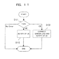
- FIG. 11 is a flowchart illustrating an operation example of an error checker according to this embodiment.
- common reference symbols to FIG. 28 denote the same or equivalent components as or to those in FIG. 28 , descriptions of which will be omitted herefrom.
- a processing step S133 is executed in this figure, in place of the processing step S113. If a CE occurs (S111, CE), an error checker corrects the CE and notifies a connected selector generation unit 12q of the CE (S133). This flow then ends.
- the error checker in the processing device 2a0q sends an error signal 16a0 to the selector generation unit 12q when a CE is detected.
- the selector generation unit 12q which has received the CE signal selects a signal 5a for the line-A from which an error has been detected and separates the line B from which no error has been detected, from the system. Thereafter, the processing device 2a0q on the line where an error has been detected corrects the CE signal, and an error log is recorded in an interruptive manner owing to the CE recording function.
- the selector generation unit 12q After recording the log, the selector generation unit 12q connects the separated line B again to the system, and resynchronizes both lines. Therefore, synchronization of the system is maintained while recording logs of CEs. Since the processing devices records logs of CEs, there is no need of a mechanism for externally reading CE logs from outside. Therefore, the CE recording unit as used in the second embodiment need not be inserted.
- the information processing system is expressed as a system board (SB) 60
- the processing devices 2a0q, 2a1q, 2b0q, and 2b1q are respectively expressed as CPU 70, CPU 71, CPU 72, and CPU 73
- the control system 1 is expressed as a north bridge 80, respectively.
- Resynchronization in this embodiment is a technique of resynchronizing a CPU in a short time (within a timeout detection period of an OS) to achieve resynchronization while the OS is running.
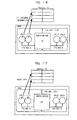
- FIG. 12 is a block diagram illustrating operation of a processing step S21 0 on a system board according to this embodiment. This figure illustrates a case that a problem occurs in the CPU 72 on the line B.
- the CPUs 70 and 72 constitute a redundant CPU pair based on synchronous operation, as well as the CPUs 71 and 73 a redundant CPU pair.
- FIG. 13 is a block diagram illustrating operation of the processing step S220 on the system board according to this embodiment.
- FIG. 14 is a block diagram illustrating operation of the processing step S230.
- the north bridge 80 hereby notifies the normal CPUs 70 and 71 of the stop of the line B.
- FIG 15 is a block diagram illustrating operation of the processing step S240 on the system board according to this embodiment.
- the north bridge 80 on the system board 60 is connected to the north bridge 81 on the system board (SB) 61 through a global address cross bar 62. If the north bridge 81 on the system board 61 issues a command to the system board 60, the command is sent through the global address cross bar 62 (S241) to the system board 60 (S242). The north bridge 80 on the system board 60, which receives the command, then issues Retry for the system board 61. This Retry is sent through the global address cross bar 62 (S243) to the system board 61 (S244).
- FIG. 16 is a block diagram illustrating operation of the processing step S250 on the system board according to this embodiment.
- the north bridge 80 hereby instructs the normal CPUs 70 and 71 to retract CPU internal information into the memory 74.
- FIG. 17 is a block diagram illustrating operation of the processing step S260 on the system board according to this embodiment.
- FIG. 18 is a block diagram illustrating operation of the processing step S270 on the system board according to this embodiment.
- FIG. 19 is a block diagram illustrating operation of the processing step S280 on the system board according to this embodiment.
- FIG. 20 is a block diagram illustrating operation of the processing step S290 on the system board according to this embodiment.
- FIG. 21 is a block diagram illustrating operation of the processing step S310 on the system board according to this embodiment.
- FIG. 22 is a block diagram illustrating operation of the processing step S320 on the system board according to this embodiment.
- the north bridge 81 when the north bridge 81 thereafter issues a command for the north bridge 80, the command is sent through the global address cross bar 62 (S321) to the north bridge 80 (S322).
- the north bridge 80 receives and processes the command, and then issues a response to the north bridge 81.
- the response is sent through the global address cross bar 62 (S323) to the north bridge 81 (S324).
- the north bridge 80 counts a number of executed resynchronizations, and sets in advance an upper limit to a number of allowable resynchronizations. When the number of executed resynchronizations > the upper limit is satisfied, the north bridge 80 only stops a problematic CPU bus without performing any more resynchronization, and continues operation of the system on one single line including only normal CPU bus.
- the second case is that initialization of CPUs and recovery of internal information are not all complete but a step-out of synchronization occurs like in the processing step S210 during resynchronization.
- the north bridge 80 suspends resynchronization and performs operation only on one single line including only normal CPU bus, and releases restriction of external commands which has been carried out in the processing step S240 (S410).
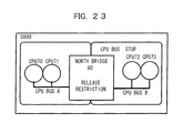
- FIG. 23 is a block diagram illustrating operation of the processing step S410 on the system board according to this embodiment.
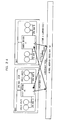
- FIG. 24 is a block diagram illustrating operation of the processing step S420 on the system board according to this embodiment. As illustrated in this figure, when the north bridge 81 thereafter issues a command for the north bridge 80, the processing steps S321 to S324 are executed.
- software of each processing device on the lines A and B has a function to record a log when a CE signal is detected.
- a CE signal is detected on one of the lines A and B, the remaining line from which the CE is not detected is separated from the system.
- more detailed error logs than in the second embodiment can be collected with use of the software of each processing device. Since collection of detailed error logs is thus achieved, application of hardware errors to predictive monitoring can be expected and lead to improvement in reliability of the mirror mode.
- the processing units correspond to the lines A and B in the embodiments.
- the detection units correspond to the error checkers in the embodiment.
- the comparison unit corresponds to a comparator in the embodiments.
- the control unit corresponds to the selector generation unit in the embodiments.
- the recording unit corresponds to the CE recording unit in the embodiments or the CE recording function of the processing device.
- the detection step corresponds to processing executed by the error checkers in the embodiments.
- the comparison step corresponds to processing executed by the comparator in the embodiments.
- the control step corresponds to processing executed by the selector generation unit in the embodiments.
- the recording step corresponds to processing executed by the CE recording unit in the embodiments or the CE recording function of the processing device.
- the resynchronization step corresponds to resynchronization in the embodiments.
Landscapes
- Engineering & Computer Science (AREA)
- Theoretical Computer Science (AREA)
- Quality & Reliability (AREA)
- Physics & Mathematics (AREA)
- General Engineering & Computer Science (AREA)
- General Physics & Mathematics (AREA)
- Hardware Redundancy (AREA)
Abstract
Description
- The present invention relates to an information processing device having plural processing devices synchronized with each other, and an error processing method.
- An information processing system using a conventional mirror mode (duplexing) will now be described. The mirror mode is an information processing technique of allowing a system to operate, even when a trouble occurs on one system, with use of another line by performing processing while synchronizing the one line (synchronized unit) with the another line.
- Now, a description will be made of a system configuration of a conventional information processing system using a mirror mode.
FIG. 25 is a block diagram illustrating a configuration example of a conventional information processing system. The information processing system is constituted by two lines A and B which perform synchronous operation, and includes acontrol system 1, processing devices 2a0 and 2a1 on the line A, and processing devices 2b0 and 2b1 on the line B. The processing devices are, for example, CPUs. The processing devices 2a0, 2a1, 2b0, and 2b1 each has an error checker inside. Thecontrol system 1 includes an interface (A IF) 4a for the line A, an interface (B IF) 4b for the line B,error checkers comparator 9, aselector generation unit 12, aselector 14, and acommon unit 15. Of these components, the processing devices 2a0, 2a1, AIF 4a, anderror checker 7a are on the line A while the processing devices 2b0, 2b1,B IF 4b, anderror checker 7b are on the line B. - The
control system 1 is connected to the processing devices 2a0 and 2a1 through aroute 3a and theA IF 4a, and is also connected to the processing devices 2b0 and 2b1 through aroute 3b and theB IF 4b. The lines A and B operate synchronously and each has three error checkers (wherein the line A includes theerror checker 7a and the error checkers in the processing devices 2a0 and 2a1, and the line B includes theerror checker 7b and the error checkers in the processing devices 2b0 and 2b1). Thecomparator 9 carries out a synchronization check between asignal 5a outputted from the line A and asignal 5b outputted from the line B. - Output of the
common unit 15 is inputted to the processing devices 2a0 and 2a1 through theA IF 4a, and to the processing devices 2b0 and 2b1 through theB IF 4b. Accordingly, a UE (uncorrectable error) in thecommon unit 15 propagates to the lines A and B when the processing devices read from the common unit. The UE is therefore detected on both the lines A and B. - The
selector generation unit 12 makes a determination based on asignal 10 outputted from thecomparator 9, asignal 8a outputted from theerror checker 7a, asignal 8b outputted from theerror checker 7b, a signal 11a0 outputted from the error checker inside the processing device 2a0, a signal 11a1 outputted from the error checker inside the processing device 2a1, a signal 11b0 outputted from the error checker inside the processing device 2b0, and a signal 11b1 outputted from the error checker inside the processing device 2b1. In accordance with asignal 13 indicating a determination result from theselector generation unit 12, theselector 14 selects and outputs either thesignal common unit 15. - Described below is a case that an error checker detects a UE.
- Next, operation of receiving an error signal by the
selector generation unit 12 will be described.FIG. 26 is a table illustrating an operation example of receiving a UE signal by a conventional selector generation unit. This table represents content of theselect signal 13 as outputted from theselector generation unit 12 in relation to content of line-A error signals (e.g., thesignals 8a, 11a0, and 11a1), line-B error signals (e.g., thesignals 8b, 11b0, and 11b1), and synchronization errors (comparison errors and the signal 10) inputted to theselector generation unit 12, for each case number. - The line-A error signals each indicates that a UE is detected by a line-A error checker, and the line-B error signals each indicates that a UE is detected by a line-B error checker. The synchronization error is an error of in synchronization between the lines A and B, and indicates that a comparison result from the
comparator 9 indicates a disagreement (i.e., being out of synchronization). Content of theselect signal 13 indicates one ofsignal 5a,signal 5b and an error stop (not selected and a system stop). If the content of theselect signal 13 describes that "both ofsignal 5a andsignal 5b are OK", theselector generation unit 12 selects either thesignal 5a orsignal 5b in accordance with a predetermined determination method because the same operation is obtained regardless of whether thesignal 5a orsignal 5b is selected. The predetermined determination method is, for example, to select a preset line or a line selected in advance. -
FIG. 27 is a flowchart illustrating an operation example when a conventional selector generation unit receives an error signal. Theselector generation unit 12 firstly determines whether a notification about a UE has been received or not (S11). - If a notification about a UE has been received (S11, Yes), the
selector generation unit 12 determines where the UE has been received from (S21). If the UE is an error from the line A (S21, line-A error), theselector generation unit 12 selects thesignal 5b (S22), and this flow ends. Otherwise, if the UE is an error from the line B (S21, line-B error), theselector generation unit 12 selects thesignal 5a (S23), and this flow ends. If the UE is an error which has been simultaneously notified of from both the lines A and B (S21, simultaneous), theselector generation unit 12 does not select any signal (S24, error stop), and this flow ends. - If any notification about an UE has not been received (S11, No), the
selector generation unit 12 makes a determination on a synchronization check result of the comparator 9 (S61). If no synchronization error occurs (S61, no error), theselector generation unit 12 selects either thesignal 5a orsignal 5b in accordance with the determination method described previously (S62), and this flow ends. Otherwise, if a synchronization error occurs (S61, synchronization error), theselector generation unit 12 does not select any signal (S63, error stop), and this flow ends. - According to the operation of the
selector generation unit 12, if a comparison error is detected or errors are detected on both lines (case number = 2, or 5 to 11 as illustrated inFIG. 26 ), the information processing system stops. - Next, operation of each error checker (the
error checkers FIG. 28 is a flowchart illustrating an operation example of a conventional error checker. The error checker firstly determines what type of error has occurred (S111). If no error has occurred (S111, No Error), the error checker does nothing, and this flow ends. If a UE has occurred (S111, UE), the error checker issues a notification about the UE to the selector generation unit 12 (S112), and this flow ends. If a CE has occurred (S111, CE), the error checker corrects the CE (S113), and this flow ends. - For example, if a UE is detected on the line B, the
selector 14 selects thesignal 5a in accordance with the operation of theselector generation unit 12 as described above, and separates the line B from which an error has been detected. In a similar manner, if a UE is detected on the line A, theselector 14 selects thesignal 5b in accordance with the operation of theselector generation unit 12 as described above, and separates the line B from which an error has been detected. In this manner, the system is protected. - A further description will be made of a case that an error checker detects a CE (correctable error). If each of the lines is given a path for carrying out a CE processing in an interruptive manner, the line where a CE has been detected performs masking of an interruption processing.
- Several of conventional techniques relevant to the present invention are fault-tolerant computer devices which shorten a pause of device operation, and a resynchronization method thereof (for example, see Patent Document 1).
- [Patent Document 1] Japanese Laid-Open Patent Publication No.
2004-046599 - However, there is a case that the mirror mode is weaker against errors than a single mode, in a system in which a UE from the
common unit 15 propagates to the lines A and B and an error is recognized by the lines A and B, and which has theselector generation unit 12 performing operation as described above, like in the information processing system described previously. - Described below is a case that the processing device 2a0 incapable of recognizing poisoning data reads resources in the
common unit 15 and read target has a UE. The poisoning data is data which is marked to indicate that an error has been detected if the error is detected in the data. In the case of the single mode, if UE is detected from a read target when the processing device 2a0 reads thecommon unit 15, thecommon unit 15 poisons the data and returns the data to the processing device 2a0. Since the processing device 2a0 cannot recognize poisoning data, the error checker inside the processing device 2a0 recognizes the data as has a UE, and can accordingly determine whether recording of an error log and continuation of the system are possible or not. In contrast, in the case of the mirror mode, if thecommon unit 15 returns poisoning data and if the error checkers inside the processing devices 2a0 and 2b0 simultaneously recognize UEs, signals 11a0 and 11b0 are simultaneously asserted because a UE is an error which causes separation of a line. The system then stops. - If each of the lines is given a path for carrying out a CE processing in an interruptive manner when a CE is detected, recording of a CE log and continuation of the system are possible upon detection of a CE signal, in the single mode. However, masking for an interruption processing for a CE is carried out in the mirror mode, and therefore, recording of a CE log cannot be carried out. This is because, if an interruption processing is inserted in on a line in order to record an error log, both of the lines cannot be mutually synchronized any more. However, the recording of an error log is very important from a viewpoint of predictive monitoring. Therefore, there is a harmful influence on reliability of the mirror mode.
- The present invention has been made to solve problems as described above, and has an object of providing an information processing device capable of improving reliability of synchronous operation, and an error processing method.
- To solve the problems described above, according to an aspect of the present invention, there is provided an information processing device having two processing units capable of operating in synchronization with each other, including: a common unit capable of outputting one identical signal to the two processing units; detection units that are respectively provided for the processing units and detect errors occurring in respectively corresponding ones of the two processing units; a comparison unit that compares outputs from the two processing units; and a control unit that controls signals from the processing units to the common unit, based on a detection result of the detection units and a comparison result of the comparison unit, and determines, if errors of one identical type are simultaneously detected by the detection units, that the errors are due to an error of the common unit.
- According to another aspect of the present invention, there is provided an information processing device having two processing units capable of operating in synchronization with each other, including: a common unit capable of outputting one identical signal to the two processing units; detection units that are respectively provided for the processing units and detect errors occurring in respectively corresponding ones of the two processing units; recording units that are respectively provided for each of the processing units and record information concerning errors detected by respectively corresponding ones of the detection units; a comparison unit that compares outputs from the two processing units; and a control unit that controls signals from the processing units to the common unit, based on a detection result of the detection units and a comparison result of the comparison unit.
- According to still another aspect of the present invention, there is provided an error processing method for performing an error processing on an information processing device, which includes two processing units capable of operating in synchronization with each other, and a common unit capable of outputting one identical signal to the two processing units, the method including: a detection step that detects errors occurring in the processing units; a comparison step that compares outputs from the two processing units; and a signal control step that controls signals from the processing units to the common unit, based on a detection result of the detection step and a comparison result of the comparison step, and determines, if errors of one identical type are simultaneously detected by the detection units, that the errors are due to an error of the common unit.
- According to still another aspect of the present invention, there is provided an error processing method for controlling an information processing device, which includes two processing units capable of operating in synchronization with each other, and a common unit capable of outputting one identical signal to the two processing units, the method including: a detection step that detects errors occurring in the processing units; a recording step that records information concerning the errors detected by the detection step; a comparison step that compares outputs from the two processing units; and a control step that controls signals from the processing units to the common unit, based on a detection result of the detection step and a comparison result of the comparison step.
-
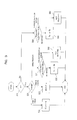
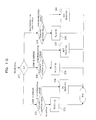
-
FIG. 1 is a block diagram illustrating a configuration example of an information processing system according to a first embodiment of the invention; -
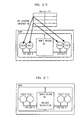
FIG. 2 is a table illustrating an operation example of receiving a UE signal by a selector generation unit according to the first embodiment; -
FIG. 3 is a flowchart illustrating an operation example of receiving an error signal by the selector generation unit according to the first embodiment; -
FIG. 4 is a block diagram illustrating a configuration example of an information processing system according to a second embodiment of the invention; -
FIG. 5 is a circuit diagram illustrating a configuration example of a CE recording unit according to the second embodiment; -
FIG. 6 is a flowchart illustrating an operation example of an error checker according to the second embodiment; -
FIG. 7 is a block diagram illustrating a configuration example of an information processing system according to a third embodiment of the invention; -
FIG. 8 is a table illustrating an operation example of receiving a CE signal by a selector generation unit according to the third embodiment; -
FIG. 9 is a flowchart illustrating a first processing in operation of receiving an error signal by the selector generation unit according to the third embodiment; -
FIG. 10 is a flowchart illustrating a second processing in the operation of receiving an error signal by the selector generation unit according to the third embodiment; -
FIG. 11 is a flowchart illustrating an operation example of an error checker according to the third embodiment; -
FIG. 12 is a block diagram illustrating operation of a processing step S210 on a system board according to the third embodiment; -
FIG. 13 is a block diagram illustrating operation of a processing step S220 on the system board according to the third embodiment; -
FIG. 14 is a block diagram illustrating operation of a processing step S230 on the system board according to the third embodiment; -
FIG. 15 is a block diagram illustrating operation of a processing step S240 on the system board according to the third embodiment; -
FIG. 16 is a block diagram illustrating operation of a processing step S250 on the system board according to the third embodiment; -
FIG. 17 is a block diagram illustrating operation of a processing step S260 on the system board according to the third embodiment; -
FIG. 18 is a block diagram illustrating operation of a processing step S270 on the system board according to the third embodiment; -
FIG. 19 is a block diagram illustrating operation of a processing step S280 on the system board according to the third embodiment; -
FIG. 20 is a block diagram illustrating operation of a processing step S290 on the system board according to the third embodiment; -
FIG. 21 is a block diagram illustrating operation of a processing step S310 on the system board according to the third embodiment; -
FIG. 22 is a block diagram illustrating operation of a processing step S320 on the system board according to the third embodiment; -
FIG. 23 is a block diagram illustrating operation of a processing step S410 on the system board according to the third embodiment; -
FIG. 24 is a block diagram illustrating operation of a processing step S420 on the system board according to the third embodiment; -
FIG. 25 is a block diagram illustrating a configuration example of a conventional information processing system; -
FIG 26 is a table illustrating an operation example of receiving a UE signal by a conventional selector generation unit; -
FIG. 27 is a flowchart illustrating an operation example of receiving an error signal by the conventional selector generation unit; and -
FIG. 28 is a flowchart illustrating an operation example of a conventional error checker. - Hereinafter, embodiments of the invention will be described with reference to the drawings.
- At first, a configuration of an information processing system (information processing device) according to an embodiment of the invention will be described.
-
FIG. 1 is a block diagram illustrating a configuration example of the information processing system according to this embodiment. In this figure, common reference symbols toFIG. 25 denote the same or equivalent components as or to those inFIG. 25 , descriptions of which will be omitted herefrom. Compared withFIG. 25 ,FIG 1 includes aselector generation unit 12p in place of theselector generation unit 12. - Next, operation of the information processing system according to this embodiment will be described.
- As in the conventional information processing system described previously, the information processing system recognizes errors on lines A and B through which UEs of a
common unit 15 propagate. - Described next is an operation of receiving an error signal by the
selector generation unit 12p. -
FIG. 2 is a table illustrating an operation example of receiving a UE signal by the selector generation unit according to this embodiment. This figure is similar toFIG. 26 but differs in that, if UEs are detected on the lines A and B and if there is no comparison error (case number = 5, 7, or 9 illustrated inFIG. 2 ), either thesignal 5a orsignal 5b is selected in accordance with the determination method described previously. -
FIG. 3 is a flowchart illustrating an operation example of receiving an error signal by the selector generation unit according to this embodiment. In this figure, common reference symbols toFIG 27 denote the same or equivalent components as or to those inFIG. 27 , descriptions of which will be omitted herefrom. Compared withFIG. 27 , a processing step S31 is executed in this figure, in place of the processing step S24. In a processing step S21, if UEs are errors received simultaneously from both the lines A and B (S21, simultaneous), theselector generation unit 12p makes a determination on a synchronization check result from the comparator 9 (S31). If there is no synchronization error (S31, no error), theselector generation unit 12p selects either thesignal 5a orsignal 5b in accordance with the method described previously (S32), and this flow then ends. Otherwise, if there is a synchronization error (S31, synchronization error), theselector generation unit 12p does not select any signal (S33, error stop), and this flow then ends. - Each of error checkers (the
error checkers FIG. 28 . - According to the
selector generation unit 12p described above, for example, the processing devices 2a0 and 2b0 read resources in thecommon unit 15. If UD is detected from a target thereof, the system is not stopped by theselector 14, unlike in the conventional information processing system described previously, but the UE is recognized as a common unit error even if both the lines A and B simultaneously detect UEs. - Even if errors are simultaneously detected on the lines A and B for some other reason, an error stop is determined in case of a comparison error (case number = 6, 8, or 10 as illustrated in
FIG.2 ) as a result of a synchronization check performed by thecomparator 9. Reliability of the system is therefore not damaged. - According to this embodiment, if a common unit error which does not necessitate stop of the system propagates to the lines A and B, the error which has propagates to the lines A and B can be recognized to be a common unit error, leading to improvement in reliability of the mirror mode.
- At first, a description will be made of the configuration of the information processing system (information processing device) according to a second embodiment.
-
FIG. 4 is a block diagram illustrating a configuration example of the information processing system according to this embodiment. In this figure, common reference symbols toFIG. 25 denote the same or equivalent components as or to those inFIG. 25 , descriptions of which will be omitted herefrom. Compared withFIG. 25 ,CE recording units 16a and 16b are newly provided in this figure. The CE recording unit 16a records logs of CEs detected by anerror checker 7a and error checkers in the processing devices 2a0 and 2a1. Similarly, theCE recording unit 16b records logs of CEs detected by anerror checker 7b and error checkers inside the processing devices 2b0 and 2b1. The logs recorded on theCE recording units 16a and 16b are read from outside the information processing system. -
FIG. 5 is a circuit diagram illustrating a configuration example of the CE recording units according to this embodiment. As illustrated in this figure, each of theCE recording units 16a and 16b is constituted by a simple counter circuit. The circuit counts and holds a number of errors by using a counter and a FF (flip-flop) each time when a CE signal is received. When the number of errors reaches a value Max, the circuit then keeps holding the number Max. - Described next is an operation of each of error checkers (the
error checkers FIG. 6 is a flowchart illustrating an operation example of error checkers according to this embodiment. In this figure, common reference symbols toFIG. 28 denote the same or equivalent components as or to those inFIG. 28 , descriptions of which will be omitted herefrom. Compared withFIG. 28 , a processing step S123 is executed in this figure, in place of the processing step S113. In the processing step S111, if a CE occurs (S111, CE), the error checker corrects the CE and causes a connected CE recording unit to record an error log (S123). This flow then ends. - According to this embodiment, the lines A and B are provided with the CE recording units. Therefore, when a CE signal is detected by the line A or B, the CE signal is corrected while recording a log of the CE, so that the system is kept running without separating any line. Accordingly, actualization of collection of error logs, and application to predictive monitoring of hardware errors by using content of errors can be expected and lead to improvement in reliability of the mirror mode.
- At first, a description will be made of the configuration of an information processing system (information processing device) according to a third embodiment.
- In the information processing system according to this embodiment, resynchronization is possible even after a line A or line B is separated from the control system, and each of the lines has a mechanism of recording logs of CEs when CEs are detected.
-
FIG. 7 is a block diagram illustrating a configuration example of the information processing system according to this embodiment. In this figure, common reference symbols toFIG. 25 denote the same or equivalent components as or to those inFIG. 25 , descriptions of which will be omitted herefrom. Compared withFIG. 25 , aselector generation unit 12q is provided in this figure, in place of theselector generation unit 12. Processing devices 2a0q, 2a1q, 2b0q, and 2b1q are provided respectively in place of the processing devices 2a0, 2a1, 2b0, and 2b1. Further, there are provided a signal 16a0 for notifying theselector generation unit 12q of an error which has occurred in the processing device 2a0q, a signal 16a1 for notifying theselector generation unit 12q of an error which has occurred in the processing device 2a1q, a signal 16b0 for notifying theselector generation unit 12q of an error which has occurred in the processing device 2b0q, and a signal 16b1 for notifying theselector generation unit 12q of an error which has occurred in the processing device 2b1q. - The processing devices 2a0q, 2a1q, 2b0q, and 2b1q are, for example, CPUs each of which has a CE recording function to record logs of CEs in an interruptive manner when CEs are detected.
- Next, operation of the information processing system according to this embodiment will be described.
- Described first is an operation of receiving a CE signal by the
selector generation unit 12q. -
FIG. 8 is a table illustrating an operation example of receiving a CE signal by the selector generation unit according to this embodiment. This table represents content of aselect signal 13 as outputted from theselector generation unit 12q in relation to content of line-A error signals (signals 16a0 and 16a1), line-B error signals (signals 16b0 and 16b1), and synchronization errors (a comparison error and a signal 10), for each case number. The content of theselect signal 13 represents thesignal 5a,signal 5b, or error stop. If the content of theselect signal 13 describes that "both of 5a and 5b are OK", theselector generation unit 12q may select either thesignal signals -
FIG. 9 is a flowchart illustrating a first processing in the operation of receiving an error signal by the selector generation unit according to this embodiment.
FIG 10 is a flowchart illustrating a second processing in the operation of receiving an error signal by the selector generation unit according to this embodiment. InFIGS. 9 and10 , common reference symbols toFIG. 27 denote the same or equivalent components as or to those inFIG 27 , descriptions of which will be omitted herefrom. Firstly, theselector generation unit 12q determines whether a notification about an error has been received or not (S1). - If a notification about an error has been received (S1, Yes), the
selector generation unit 12q determines whether the notification includes a UE or not (S2). If a UE is included in the notification (S2, UE), theselector generation unit 12q executes the same processing as the conventional processing from the processing step S21 thereof. If a CE is included in the notification (S2, CE Only), theselector generation unit 12q determines where the CE has occurred (S71). - If the CE is an error from the line A in the processing step S71 (S71, line-A error), the
selector generation unit 12q determines a synchronization check result from thecomparator 9. If there is no synchronization error (S72, no error), theselector generation unit 12q selects thesignal 5a (S73). If there is a synchronization error (S72, synchronization error), no signal is selected (S74, error stop) and this flow ends. - Alternatively, if the CE is an error from the line B in the processing step S71 (S71, line-B error), the
selector generation unit 12q makes a determination on a synchronization check result from thecomparator 9. If there is no synchronization error (S75, no error), theselector generation unit 12q selects thesignal 5b (S76). Otherwise, if there is a synchronization error (S75, synchronization error), no signal is selected (S77, error stop) and this flow ends. - Also alternatively, if the CE is an error which has been simultaneously notified of from both the lines A and B (S71, simultaneous), the
selector generation unit 12q makes a determination on a synchronization check result from thecomparator 9. If there is no synchronization error (S78, no error), either thesignal - If no notification about an error has been received (S1, No), the
selector generation unit 12q executes the same processing as the conventional processing from the processing step S61 thereof. - Described next is an operation of each of error checkers (
error checkers FIG. 11 is a flowchart illustrating an operation example of an error checker according to this embodiment. In this figure, common reference symbols toFIG. 28 denote the same or equivalent components as or to those inFIG. 28 , descriptions of which will be omitted herefrom. Compared withFIG. 28 , a processing step S133 is executed in this figure, in place of the processing step S113. If a CE occurs (S111, CE), an error checker corrects the CE and notifies a connectedselector generation unit 12q of the CE (S133). This flow then ends. - The error checker in the processing device 2a0q sends an error signal 16a0 to the
selector generation unit 12q when a CE is detected. Theselector generation unit 12q which has received the CE signal selects asignal 5a for the line-A from which an error has been detected and separates the line B from which no error has been detected, from the system. Thereafter, the processing device 2a0q on the line where an error has been detected corrects the CE signal, and an error log is recorded in an interruptive manner owing to the CE recording function. - After recording the log, the
selector generation unit 12q connects the separated line B again to the system, and resynchronizes both lines. Therefore, synchronization of the system is maintained while recording logs of CEs. Since the processing devices records logs of CEs, there is no need of a mechanism for externally reading CE logs from outside. Therefore, the CE recording unit as used in the second embodiment need not be inserted. - Next, an operation example of resynchronization will be described.
- In the following, operation of the resynchronization will be described referring to an example in which the information processing system according to this embodiment is expressed as a system board (SB) 60, the processing devices 2a0q, 2a1q, 2b0q, and 2b1q are respectively expressed as CPU 70,
CPU 71,CPU 72, andCPU 73, and thecontrol system 1 is expressed as anorth bridge 80, respectively. - Resynchronization in this embodiment is a technique of resynchronizing a CPU in a short time (within a timeout detection period of an OS) to achieve resynchronization while the OS is running.
- At first, the
north bridge 80 detects a step-out of redundancy (synchronization) due to an error of the CPU on one line (S210).FIG. 12 is a block diagram illustrating operation of a processing step S21 0 on a system board according to this embodiment. This figure illustrates a case that a problem occurs in theCPU 72 on the line B. TheCPUs 70 and 72 constitute a redundant CPU pair based on synchronous operation, as well as theCPUs 71 and 73 a redundant CPU pair. - Next, the
north bridge 80 stops operation of the CPU bus connected to theproblematic CPU 72, and also stops commands from being thereafter issued from the CPU bus (S220).FIG. 13 is a block diagram illustrating operation of the processing step S220 on the system board according to this embodiment. - Next, the
north bridge 80 notifies the other paired normal CPU bus constituting the redundant structure of the stop of one line (S230).FIG. 14 is a block diagram illustrating operation of the processing step S230. Thenorth bridge 80 hereby notifies thenormal CPUs 70 and 71 of the stop of the line B. - Next, to restrict commands from outside, the
north bridge 80 continues to retry external commands (S240).FIG 15 is a block diagram illustrating operation of the processing step S240 on the system board according to this embodiment. As illustrated in this figure, thenorth bridge 80 on the system board 60 is connected to thenorth bridge 81 on the system board (SB) 61 through a globaladdress cross bar 62. If thenorth bridge 81 on thesystem board 61 issues a command to the system board 60, the command is sent through the global address cross bar 62 (S241) to the system board 60 (S242). Thenorth bridge 80 on the system board 60, which receives the command, then issues Retry for thesystem board 61. This Retry is sent through the global address cross bar 62 (S243) to the system board 61 (S244). - Next, the
north bridge 80 issues a firmware instruction so as to retract CPU internal information which is least necessary for resynchronization, into the memory from the normal CPUs (S250).FIG. 16 is a block diagram illustrating operation of the processing step S250 on the system board according to this embodiment. Thenorth bridge 80 hereby instructs thenormal CPUs 70 and 71 to retract CPU internal information into thememory 74. - Next, the
normal CPUs 70 and 71 which have received the instruction from thenorth bridge 80 writes cache data (CPU internal information) into thememory 74 in accordance with the instruction (S260).FIG. 17 is a block diagram illustrating operation of the processing step S260 on the system board according to this embodiment. - Next, the
north bridge 80 then clears a snoop tag (cache state information of respective CPUs) in thenorth bridge 80 at the time when writing of cache data from all normal CPUs into the memory is completed (S270).FIG. 18 is a block diagram illustrating operation of the processing step S270 on the system board according to this embodiment. - Next, the
north bridge 80 issues CPU Reset simultaneously for each of theCPUs FIG. 19 is a block diagram illustrating operation of the processing step S280 on the system board according to this embodiment. - Next, the
north bridge 80 initializes each of theCPUs FIG. 20 is a block diagram illustrating operation of the processing step S290 on the system board according to this embodiment. - Depending on a state at this time, one of the following two cases is executed.
- The first case is that initialization and recovery of internal information are completed for all the CPUs. At this time, the
north bridge 80 releases restriction on external commands, which has been executed in the processing step S240 (S310).FIG. 21 is a block diagram illustrating operation of the processing step S310 on the system board according to this embodiment. - Next, the
north bridge 80 restarts operation (S320), and resynchronization then ends.FIG. 22 is a block diagram illustrating operation of the processing step S320 on the system board according to this embodiment. As illustrated in this figure, when thenorth bridge 81 thereafter issues a command for thenorth bridge 80, the command is sent through the global address cross bar 62 (S321) to the north bridge 80 (S322). Thenorth bridge 80 receives and processes the command, and then issues a response to thenorth bridge 81. The response is sent through the global address cross bar 62 (S323) to the north bridge 81 (S324). - The
north bridge 80 counts a number of executed resynchronizations, and sets in advance an upper limit to a number of allowable resynchronizations. When the number of executed resynchronizations > the upper limit is satisfied, thenorth bridge 80 only stops a problematic CPU bus without performing any more resynchronization, and continues operation of the system on one single line including only normal CPU bus. - The second case is that initialization of CPUs and recovery of internal information are not all complete but a step-out of synchronization occurs like in the processing step S210 during resynchronization. In this case, the
north bridge 80 suspends resynchronization and performs operation only on one single line including only normal CPU bus, and releases restriction of external commands which has been carried out in the processing step S240 (S410).FIG. 23 is a block diagram illustrating operation of the processing step S410 on the system board according to this embodiment. - Next, the
north bridge 80 restarts operation (S420), and the resynchronization ends.FIG. 24 is a block diagram illustrating operation of the processing step S420 on the system board according to this embodiment. As illustrated in this figure, when thenorth bridge 81 thereafter issues a command for thenorth bridge 80, the processing steps S321 to S324 are executed. - According to this embodiment, software of each processing device on the lines A and B has a function to record a log when a CE signal is detected. When a CE signal is detected on one of the lines A and B, the remaining line from which the CE is not detected is separated from the system. In this manner, more detailed error logs than in the second embodiment can be collected with use of the software of each processing device. Since collection of detailed error logs is thus achieved, application of hardware errors to predictive monitoring can be expected and lead to improvement in reliability of the mirror mode.
- The first, second, and third embodiments described above may be combined with each other.
- The processing units correspond to the lines A and B in the embodiments. The detection units correspond to the error checkers in the embodiment. The comparison unit corresponds to a comparator in the embodiments. The control unit corresponds to the selector generation unit in the embodiments. The recording unit corresponds to the CE recording unit in the embodiments or the CE recording function of the processing device.
- The detection step corresponds to processing executed by the error checkers in the embodiments. The comparison step corresponds to processing executed by the comparator in the embodiments. The control step corresponds to processing executed by the selector generation unit in the embodiments. The recording step corresponds to processing executed by the CE recording unit in the embodiments or the CE recording function of the processing device. The resynchronization step corresponds to resynchronization in the embodiments.
- As has been described above, reliability of resynchronization operation can be improved according to the present invention.
Claims (20)
- An information processing device having two processing units capable of operating in synchronization with each other, comprising:a common unit capable of outputting one identical signal to the two processing units;detection units that are respectively provided for the processing units and detect errors occurring in respectively corresponding ones of the two processing units;a comparison unit that compares outputs from the two processing units; anda control unit that controls signals from the processing units to the common unit, based on a detection result of the detection units and a comparison result of the comparison unit, and determines, if errors of one identical type are simultaneously detected by the detection units, that the errors are due to an error of the common unit.
- The information processing device according to claim 1, wherein the errors of one identical type are uncorrectable errors (UEs).
- The information processing device according to claim 2, wherein if UEs are detected simultaneously by the detection units respectively corresponding to the two processing units and if the comparison unit determines the outputs from the two processing units to be synchronous with each other, the control unit determines that the UEs are due to an error of the common unit.
- The information processing device according to claim 1, wherein
at least one processor is provided for each of the processing units, and
the detection units are respectively provided at least in the processors, respectively. - An information processing device having two processing units capable of operating in synchronization with each other, comprising:a common unit capable of outputting one identical signal to the two processing units;detection units that are respectively provided for the processing units and detect errors occurring in respectively corresponding ones of the two processing units;recording units that are respectively provided for each of the processing units and record information concerning errors detected by respectively corresponding ones of the detection units;a comparison unit that compares outputs from the two processing units; anda control unit that controls signals from the processing units to the common unit, based on a detection result of the detection units and a comparison result of the comparison unit.
- The information processing device according to claim 5, wherein the recording units record information concerning correctable errors (CEs) detected by respectively corresponding ones of the detection units.
- The information processing device according to claim 6, wherein
the recording units each have a counter, and
the information concerning CEs is a number of CEs. - The information processing device according to claim 6, wherein if a CE is detected by one of the detection units,
the control unit transfers signals to the common unit from one of the two processing units from which the CE is detected,
one of the recording units corresponding to the one of the two processing units form which the CE is detected records information concerning the CE detected by the one of the detection units, and
the common unit resynchronizes the two processing units. - The information processing device according to claim 8, wherein the recording units are software which is executed by respectively corresponding ones of the processing units.
- The information processing device according to claim 9, wherein the recording units are interruption processings executed in respectively corresponding ones of the processing units.
- An error processing method for performing an error processing on an information processing device, which includes two processing units capable of operating in synchronization with each other, and a common unit capable of outputting one identical signal to the two processing units, the method comprising:a detection step that detects errors occurring in the processing units;a comparison step that compares outputs from the two processing units; anda signal control step that controls signals from the processing units to the common unit, based on a detection result of the detection step and a comparison result of the comparison step, and determines, if errors of one identical type are simultaneously detected by the detection units, that the errors are due to an error of the common unit.
- The error processing method according to claim 11, wherein the errors of one identical type are uncorrectable errors (UEs).
- The error processing method according to claim 12, wherein if UEs are detected simultaneously through the detection step by the two processing units and if the comparison step determines the outputs from the two processing units to be synchronous with each other, the control step determines that the UEs are due to an error of the common unit.
- The error processing method according to claim 11, wherein
at least one processor is provided for each of the processing units, and
the detection step is executed at least in the processors. - An error processing method for controlling an information processing device, which includes two processing units capable of operating in synchronization with each other, and a common unit capable of outputting one identical signal to the two processing units, the method comprising:a detection step that detects errors occurring in the processing units;a recording step that records information concerning the errors detected by the detection step;a comparison step that compares outputs from the two processing units; anda control step that controls signals from the processing units to the common unit, based on a detection result of the detection step and a comparison result of the comparison step.
- The error processing method according to claim 15, wherein the recording step records information concerning correctable errors (CEs) detected by the detection step.
- The error processing method according to claim 16, wherein the information concerning CEs is a number of CEs.
- The error processing method according to claim 16, wherein if a CE is detected by the detection step,
the control step transfers a signal to the common unit from one of the two processing units from which the CE is detected,
the recording step records information concerning the CE detected by the detection step, and the method further comprises
a resynchronization step that resynchronizes the two processing units. - The error processing method according to claim 18, wherein the recording step is software which is executed by corresponding one of the processing units.
- The error processing method according to claim 19, wherein the recording step is an interruption processing executed in corresponding one of the processing units.
Priority Applications (1)
| Application Number | Priority Date | Filing Date | Title |
|---|---|---|---|
| EP11163540A EP2372554B1 (en) | 2007-03-29 | 2007-03-29 | Information processing device and error processing method |
Applications Claiming Priority (1)
| Application Number | Priority Date | Filing Date | Title |
|---|---|---|---|
| PCT/JP2007/056858 WO2008120352A1 (en) | 2007-03-29 | 2007-03-29 | Information processing apparatus and error processing method |
Related Child Applications (1)
| Application Number | Title | Priority Date | Filing Date |
|---|---|---|---|
| EP11163540.5 Division-Into | 2011-04-21 |
Publications (3)
| Publication Number | Publication Date |
|---|---|
| EP2141596A1 true EP2141596A1 (en) | 2010-01-06 |
| EP2141596A4 EP2141596A4 (en) | 2010-10-27 |
| EP2141596B1 EP2141596B1 (en) | 2011-12-14 |
Family
ID=39807945
Family Applications (2)
| Application Number | Title | Priority Date | Filing Date |
|---|---|---|---|
| EP11163540A Not-in-force EP2372554B1 (en) | 2007-03-29 | 2007-03-29 | Information processing device and error processing method |
| EP07740296A Not-in-force EP2141596B1 (en) | 2007-03-29 | 2007-03-29 | Information processing apparatus and error processing method |
Family Applications Before (1)
| Application Number | Title | Priority Date | Filing Date |
|---|---|---|---|
| EP11163540A Not-in-force EP2372554B1 (en) | 2007-03-29 | 2007-03-29 | Information processing device and error processing method |
Country Status (5)
| Country | Link |
|---|---|
| US (1) | US8078920B2 (en) |
| EP (2) | EP2372554B1 (en) |
| JP (1) | JP4629793B2 (en) |
| AT (1) | ATE537502T1 (en) |
| WO (1) | WO2008120352A1 (en) |
Cited By (1)
| Publication number | Priority date | Publication date | Assignee | Title |
|---|---|---|---|---|
| EP2204736A4 (en) * | 2007-09-25 | 2012-01-11 | Fujitsu Ltd | INFORMATION PROCESSOR AND CONTROL METHOD |
Families Citing this family (5)
| Publication number | Priority date | Publication date | Assignee | Title |
|---|---|---|---|---|
| JP2963076B2 (en) | 1998-01-28 | 1999-10-12 | 株式会社フジワラテクノアート | Cleaning equipment for brewing machines with rotating discs |
| JP5278530B2 (en) * | 2009-03-09 | 2013-09-04 | 富士通株式会社 | Information processing apparatus, information processing apparatus control method, and information processing apparatus control program |
| DE102010048352B3 (en) * | 2010-10-13 | 2012-04-26 | Fujitsu Technology Solutions Intellectual Property Gmbh | Interface monitoring device for an interface connection and use of an interface monitoring device |
| US10649829B2 (en) * | 2017-07-10 | 2020-05-12 | Hewlett Packard Enterprise Development Lp | Tracking errors associated with memory access operations |
| JP6923250B2 (en) * | 2018-12-14 | 2021-08-18 | Necプラットフォームズ株式会社 | System and encryption processing method |
Family Cites Families (38)
| Publication number | Priority date | Publication date | Assignee | Title |
|---|---|---|---|---|
| US4965717A (en) * | 1988-12-09 | 1990-10-23 | Tandem Computers Incorporated | Multiple processor system having shared memory with private-write capability |
| US5295258A (en) * | 1989-12-22 | 1994-03-15 | Tandem Computers Incorporated | Fault-tolerant computer system with online recovery and reintegration of redundant components |
| JP2559531B2 (en) * | 1990-10-18 | 1996-12-04 | 富士通株式会社 | Redundant system error check circuit |
| JPH04302332A (en) | 1991-03-29 | 1992-10-26 | Toshiba Corp | Synchronizing system for dual cpu system |
| FR2686991A1 (en) * | 1992-02-05 | 1993-07-30 | Sextant Avionique | METHOD, SYSTEM AND PROCESSOR FOR COMMUNICATING BETWEEN A PLURALITY OF SUBASSEMBLIES OF EQUIPMENT |
| US5809533A (en) * | 1993-02-18 | 1998-09-15 | Unisys Corporation | Dual bus system with multiple processors having data coherency maintenance |
| JPH07271626A (en) * | 1994-03-28 | 1995-10-20 | Toshiba Corp | Digital control system |
| FR2721122B1 (en) * | 1994-06-14 | 1996-07-12 | Commissariat Energie Atomique | Calculation unit with plurality of redundant computers. |
| EP0729097A1 (en) * | 1995-02-07 | 1996-08-28 | Sun Microsystems, Inc. | Method and apparatus for run-time memory access checking and memory leak detection of a multi-threaded program |
| KR100234504B1 (en) * | 1995-09-18 | 1999-12-15 | 포만 제프리 엘 | Integrated test method and integrated magnetic test device for capturing fault information on selected faults |
| DE19809089A1 (en) * | 1998-02-25 | 1999-08-26 | Siemens Ag | Process for synchronising and/or data exchange for secure high access computer in multi computer system |
| FR2797964B1 (en) * | 1999-08-23 | 2002-03-29 | Thomson Csf Sextant | SECURE DATA SWITCHING CONTROL DEVICE |
| US6543016B1 (en) * | 1999-11-04 | 2003-04-01 | Agere Systems Inc. | Testing content-addressable memories |
| JP4302332B2 (en) | 2000-05-19 | 2009-07-22 | 理想科学工業株式会社 | Method for making heat-sensitive stencil sheet, plate-making apparatus and stencil printing plate |
| JP2002014943A (en) | 2000-06-30 | 2002-01-18 | Nippon Telegr & Teleph Corp <Ntt> | Fault-tolerant system and fault detection method thereof |
| DE10040389A1 (en) * | 2000-08-18 | 2002-03-07 | Infineon Technologies Ag | High speed data processor for XDSL data transmission, has directly addressable input and output intermediate interface memories |
| JP3537087B2 (en) * | 2000-09-29 | 2004-06-14 | Necエレクトロニクス株式会社 | Semiconductor device and method of inspecting semiconductor device |
| FR2819598B1 (en) * | 2001-01-16 | 2003-04-11 | Thomson Csf | FAULT-TOLERANT SYNCHRONIZATION DEVICE FOR A REAL-TIME COMPUTER NETWORK |
| US7065672B2 (en) * | 2001-03-28 | 2006-06-20 | Stratus Technologies Bermuda Ltd. | Apparatus and methods for fault-tolerant computing using a switching fabric |
| US7194556B2 (en) * | 2001-03-30 | 2007-03-20 | Intel Corporation | Method and apparatus for high accuracy distributed time synchronization using processor tick counters |
| GB2377024A (en) * | 2001-06-29 | 2002-12-31 | Motorola Inc | Fault tolerant measurment data outputting system |
| EP1376356A1 (en) * | 2002-06-26 | 2004-01-02 | Fujitsu Siemens Computers, LLC | Error reporting network in multiprocessor computer |
| JP2004046599A (en) | 2002-07-12 | 2004-02-12 | Nec Corp | Fault tolerant computer apparatus, resynchronization method and resynchronization program |
| JP3640187B2 (en) * | 2002-07-29 | 2005-04-20 | 日本電気株式会社 | Fault processing method for multiprocessor system, multiprocessor system and node |
| US7055060B2 (en) * | 2002-12-19 | 2006-05-30 | Intel Corporation | On-die mechanism for high-reliability processor |
| JP4155088B2 (en) * | 2003-04-18 | 2008-09-24 | 日本電気株式会社 | Information processing device |
| JP4153838B2 (en) | 2003-07-04 | 2008-09-24 | 株式会社東芝 | Function and performance limiting device for image forming apparatus |
| JP2005165807A (en) * | 2003-12-04 | 2005-06-23 | Hitachi Ltd | Operation comparison method in processor multiplexing system |
| US8799706B2 (en) * | 2004-03-30 | 2014-08-05 | Hewlett-Packard Development Company, L.P. | Method and system of exchanging information between processors |
| GB0411054D0 (en) * | 2004-05-18 | 2004-06-23 | Ricardo Uk Ltd | Fault tolerant data processing |
| JP4168403B2 (en) * | 2004-12-21 | 2008-10-22 | 日本電気株式会社 | Fault tolerant system, control device used therefor, access control method, and control program |
| JP3897047B2 (en) * | 2005-01-31 | 2007-03-22 | 横河電機株式会社 | Information processing apparatus and information processing method |
| US8595557B2 (en) * | 2005-02-23 | 2013-11-26 | International Business Machines Corporation | Method and apparatus for verifying memory testing software |
| JP4667093B2 (en) * | 2005-03-17 | 2011-04-06 | 富士通株式会社 | Dual storage device and control method of dual storage device |
| JP4330547B2 (en) * | 2005-03-17 | 2009-09-16 | 富士通株式会社 | Information processing system control method, information processing system, information processing system control program, and redundant configuration control device |
| JP4667092B2 (en) * | 2005-03-17 | 2011-04-06 | 富士通株式会社 | Information processing apparatus and data control method in information processing apparatus |
| US7350007B2 (en) * | 2005-04-05 | 2008-03-25 | Hewlett-Packard Development Company, L.P. | Time-interval-based system and method to determine if a device error rate equals or exceeds a threshold error rate |
| US8826288B2 (en) * | 2005-04-19 | 2014-09-02 | Hewlett-Packard Development Company, L.P. | Computing with both lock-step and free-step processor modes |
-
2007
- 2007-03-29 AT AT07740296T patent/ATE537502T1/en active
- 2007-03-29 WO PCT/JP2007/056858 patent/WO2008120352A1/en not_active Ceased
- 2007-03-29 EP EP11163540A patent/EP2372554B1/en not_active Not-in-force
- 2007-03-29 EP EP07740296A patent/EP2141596B1/en not_active Not-in-force
- 2007-03-29 JP JP2009507343A patent/JP4629793B2/en not_active Expired - Fee Related
-
2009
- 2009-09-04 US US12/554,318 patent/US8078920B2/en not_active Expired - Fee Related
Cited By (1)
| Publication number | Priority date | Publication date | Assignee | Title |
|---|---|---|---|---|
| EP2204736A4 (en) * | 2007-09-25 | 2012-01-11 | Fujitsu Ltd | INFORMATION PROCESSOR AND CONTROL METHOD |
Also Published As
| Publication number | Publication date |
|---|---|
| US8078920B2 (en) | 2011-12-13 |
| ATE537502T1 (en) | 2011-12-15 |
| WO2008120352A1 (en) | 2008-10-09 |
| EP2141596B1 (en) | 2011-12-14 |
| EP2141596A4 (en) | 2010-10-27 |
| JP4629793B2 (en) | 2011-02-09 |
| JPWO2008120352A1 (en) | 2010-07-15 |
| US20100077262A1 (en) | 2010-03-25 |
| EP2372554A2 (en) | 2011-10-05 |
| EP2372554A3 (en) | 2012-01-18 |
| EP2372554B1 (en) | 2013-03-20 |
Similar Documents
| Publication | Publication Date | Title |
|---|---|---|
| KR100566338B1 (en) | Fault tolerant computer system, re-synchronization method thereof and computer-readable storage medium having re-synchronization program thereof recorded thereon | |
| EP2141596B1 (en) | Information processing apparatus and error processing method | |
| KR101121116B1 (en) | Synchronization control apparatus, information processing apparatus, and synchronization management method | |
| JP2006178557A (en) | Computer system and error handling method | |
| US7500139B2 (en) | Securing time for identifying cause of asynchronism in fault-tolerant computer | |
| JP2006195821A (en) | Information processing system control method, information processing system, direct memory access control device, program | |
| JP5287974B2 (en) | Arithmetic processing system, resynchronization method, and farm program | |
| US20040221195A1 (en) | Information processing apparatus | |
| US5742851A (en) | Information processing system having function to detect fault in external bus | |
| JP2004046455A (en) | Information processor | |
| KR100583214B1 (en) | Information processing apparatus | |
| JP5278530B2 (en) | Information processing apparatus, information processing apparatus control method, and information processing apparatus control program | |
| JP2019079263A (en) | Redundant-system storage system and failure recovery method for redundant-system storage system | |
| JP2941387B2 (en) | Multiplexing unit matching control method | |
| JPH1027115A (en) | Fault information sampling circuit for computer system | |
| JP5863030B2 (en) | Non-instantaneous switching device and method | |
| JP2663624B2 (en) | Instantaneous interruption switching method of redundant circuit | |
| CN115617663A (en) | Test method, device and electronic equipment for pulse voting function | |
| CN120540880A (en) | A communication method and related equipment | |
| JPH08272752A (en) | Parallel processor | |
| JPS6143739B2 (en) | ||
| JPS6339065A (en) | Data transfer device | |
| JPS61154332A (en) | Data transmitter | |
| JPH08272637A (en) | Duplex system | |
| JPS6290069A (en) | Time switch with majority logic redundant construction |
Legal Events
| Date | Code | Title | Description |
|---|---|---|---|
| PUAI | Public reference made under article 153(3) epc to a published international application that has entered the european phase |
Free format text: ORIGINAL CODE: 0009012 |
|
| 17P | Request for examination filed |
Effective date: 20091026 |
|
| AK | Designated contracting states |
Kind code of ref document: A1 Designated state(s): AT BE BG CH CY CZ DE DK EE ES FI FR GB GR HU IE IS IT LI LT LU LV MC MT NL PL PT RO SE SI SK TR |
|
| DAX | Request for extension of the european patent (deleted) | ||
| A4 | Supplementary search report drawn up and despatched |
Effective date: 20100923 |
|
| GRAP | Despatch of communication of intention to grant a patent |
Free format text: ORIGINAL CODE: EPIDOSNIGR1 |
|
| RIC1 | Information provided on ipc code assigned before grant |
Ipc: G06F 11/16 20060101ALI20110517BHEP Ipc: G06F 11/18 20060101AFI20110517BHEP |
|
| GRAS | Grant fee paid |
Free format text: ORIGINAL CODE: EPIDOSNIGR3 |
|
| GRAA | (expected) grant |
Free format text: ORIGINAL CODE: 0009210 |
|
| AK | Designated contracting states |
Kind code of ref document: B1 Designated state(s): AT BE BG CH CY CZ DE DK EE ES FI FR GB GR HU IE IS IT LI LT LU LV MC MT NL PL PT RO SE SI SK TR |
|
| REG | Reference to a national code |
Ref country code: GB Ref legal event code: FG4D |
|
| REG | Reference to a national code |
Ref country code: CH Ref legal event code: EP |
|
| REG | Reference to a national code |
Ref country code: IE Ref legal event code: FG4D |
|
| REG | Reference to a national code |
Ref country code: DE Ref legal event code: R096 Ref document number: 602007019347 Country of ref document: DE Effective date: 20120308 |
|
| REG | Reference to a national code |
Ref country code: NL Ref legal event code: VDEP Effective date: 20111214 |
|
| PG25 | Lapsed in a contracting state [announced via postgrant information from national office to epo] |
Ref country code: LT Free format text: LAPSE BECAUSE OF FAILURE TO SUBMIT A TRANSLATION OF THE DESCRIPTION OR TO PAY THE FEE WITHIN THE PRESCRIBED TIME-LIMIT Effective date: 20111214 |
|
| LTIE | Lt: invalidation of european patent or patent extension |
Effective date: 20111214 |
|
| PG25 | Lapsed in a contracting state [announced via postgrant information from national office to epo] |
Ref country code: GR Free format text: LAPSE BECAUSE OF FAILURE TO SUBMIT A TRANSLATION OF THE DESCRIPTION OR TO PAY THE FEE WITHIN THE PRESCRIBED TIME-LIMIT Effective date: 20120315 Ref country code: SI Free format text: LAPSE BECAUSE OF FAILURE TO SUBMIT A TRANSLATION OF THE DESCRIPTION OR TO PAY THE FEE WITHIN THE PRESCRIBED TIME-LIMIT Effective date: 20111214 Ref country code: NL Free format text: LAPSE BECAUSE OF FAILURE TO SUBMIT A TRANSLATION OF THE DESCRIPTION OR TO PAY THE FEE WITHIN THE PRESCRIBED TIME-LIMIT Effective date: 20111214 Ref country code: SE Free format text: LAPSE BECAUSE OF FAILURE TO SUBMIT A TRANSLATION OF THE DESCRIPTION OR TO PAY THE FEE WITHIN THE PRESCRIBED TIME-LIMIT Effective date: 20111214 Ref country code: LV Free format text: LAPSE BECAUSE OF FAILURE TO SUBMIT A TRANSLATION OF THE DESCRIPTION OR TO PAY THE FEE WITHIN THE PRESCRIBED TIME-LIMIT Effective date: 20111214 |
|
| PG25 | Lapsed in a contracting state [announced via postgrant information from national office to epo] |
Ref country code: BE Free format text: LAPSE BECAUSE OF FAILURE TO SUBMIT A TRANSLATION OF THE DESCRIPTION OR TO PAY THE FEE WITHIN THE PRESCRIBED TIME-LIMIT Effective date: 20111214 Ref country code: CY Free format text: LAPSE BECAUSE OF FAILURE TO SUBMIT A TRANSLATION OF THE DESCRIPTION OR TO PAY THE FEE WITHIN THE PRESCRIBED TIME-LIMIT Effective date: 20111214 |
|
| PG25 | Lapsed in a contracting state [announced via postgrant information from national office to epo] |
Ref country code: IS Free format text: LAPSE BECAUSE OF FAILURE TO SUBMIT A TRANSLATION OF THE DESCRIPTION OR TO PAY THE FEE WITHIN THE PRESCRIBED TIME-LIMIT Effective date: 20120414 Ref country code: BG Free format text: LAPSE BECAUSE OF FAILURE TO SUBMIT A TRANSLATION OF THE DESCRIPTION OR TO PAY THE FEE WITHIN THE PRESCRIBED TIME-LIMIT Effective date: 20120314 Ref country code: CZ Free format text: LAPSE BECAUSE OF FAILURE TO SUBMIT A TRANSLATION OF THE DESCRIPTION OR TO PAY THE FEE WITHIN THE PRESCRIBED TIME-LIMIT Effective date: 20111214 Ref country code: SK Free format text: LAPSE BECAUSE OF FAILURE TO SUBMIT A TRANSLATION OF THE DESCRIPTION OR TO PAY THE FEE WITHIN THE PRESCRIBED TIME-LIMIT Effective date: 20111214 Ref country code: EE Free format text: LAPSE BECAUSE OF FAILURE TO SUBMIT A TRANSLATION OF THE DESCRIPTION OR TO PAY THE FEE WITHIN THE PRESCRIBED TIME-LIMIT Effective date: 20111214 |
|
| PG25 | Lapsed in a contracting state [announced via postgrant information from national office to epo] |
Ref country code: RO Free format text: LAPSE BECAUSE OF FAILURE TO SUBMIT A TRANSLATION OF THE DESCRIPTION OR TO PAY THE FEE WITHIN THE PRESCRIBED TIME-LIMIT Effective date: 20111214 Ref country code: PL Free format text: LAPSE BECAUSE OF FAILURE TO SUBMIT A TRANSLATION OF THE DESCRIPTION OR TO PAY THE FEE WITHIN THE PRESCRIBED TIME-LIMIT Effective date: 20111214 Ref country code: PT Free format text: LAPSE BECAUSE OF FAILURE TO SUBMIT A TRANSLATION OF THE DESCRIPTION OR TO PAY THE FEE WITHIN THE PRESCRIBED TIME-LIMIT Effective date: 20120416 |
|
| REG | Reference to a national code |
Ref country code: AT Ref legal event code: MK05 Ref document number: 537502 Country of ref document: AT Kind code of ref document: T Effective date: 20111214 |
|
| PLBE | No opposition filed within time limit |
Free format text: ORIGINAL CODE: 0009261 |
|
| STAA | Information on the status of an ep patent application or granted ep patent |
Free format text: STATUS: NO OPPOSITION FILED WITHIN TIME LIMIT |
|
| PG25 | Lapsed in a contracting state [announced via postgrant information from national office to epo] |
Ref country code: DK Free format text: LAPSE BECAUSE OF FAILURE TO SUBMIT A TRANSLATION OF THE DESCRIPTION OR TO PAY THE FEE WITHIN THE PRESCRIBED TIME-LIMIT Effective date: 20111214 Ref country code: MC Free format text: LAPSE BECAUSE OF NON-PAYMENT OF DUE FEES Effective date: 20120331 |
|
| REG | Reference to a national code |
Ref country code: CH Ref legal event code: PL |
|
| 26N | No opposition filed |
Effective date: 20120917 |
|
| PG25 | Lapsed in a contracting state [announced via postgrant information from national office to epo] |
Ref country code: IT Free format text: LAPSE BECAUSE OF FAILURE TO SUBMIT A TRANSLATION OF THE DESCRIPTION OR TO PAY THE FEE WITHIN THE PRESCRIBED TIME-LIMIT Effective date: 20111214 |
|
| REG | Reference to a national code |
Ref country code: IE Ref legal event code: MM4A |
|
| REG | Reference to a national code |
Ref country code: DE Ref legal event code: R097 Ref document number: 602007019347 Country of ref document: DE Effective date: 20120917 |
|
| PG25 | Lapsed in a contracting state [announced via postgrant information from national office to epo] |
Ref country code: LI Free format text: LAPSE BECAUSE OF NON-PAYMENT OF DUE FEES Effective date: 20120331 Ref country code: IE Free format text: LAPSE BECAUSE OF NON-PAYMENT OF DUE FEES Effective date: 20120329 Ref country code: CH Free format text: LAPSE BECAUSE OF NON-PAYMENT OF DUE FEES Effective date: 20120331 Ref country code: AT Free format text: LAPSE BECAUSE OF FAILURE TO SUBMIT A TRANSLATION OF THE DESCRIPTION OR TO PAY THE FEE WITHIN THE PRESCRIBED TIME-LIMIT Effective date: 20111214 |
|
| PG25 | Lapsed in a contracting state [announced via postgrant information from national office to epo] |
Ref country code: ES Free format text: LAPSE BECAUSE OF FAILURE TO SUBMIT A TRANSLATION OF THE DESCRIPTION OR TO PAY THE FEE WITHIN THE PRESCRIBED TIME-LIMIT Effective date: 20120325 |
|
| PG25 | Lapsed in a contracting state [announced via postgrant information from national office to epo] |
Ref country code: FI Free format text: LAPSE BECAUSE OF FAILURE TO SUBMIT A TRANSLATION OF THE DESCRIPTION OR TO PAY THE FEE WITHIN THE PRESCRIBED TIME-LIMIT Effective date: 20111214 |
|
| PG25 | Lapsed in a contracting state [announced via postgrant information from national office to epo] |
Ref country code: MT Free format text: LAPSE BECAUSE OF FAILURE TO SUBMIT A TRANSLATION OF THE DESCRIPTION OR TO PAY THE FEE WITHIN THE PRESCRIBED TIME-LIMIT Effective date: 20111214 |
|
| PG25 | Lapsed in a contracting state [announced via postgrant information from national office to epo] |
Ref country code: TR Free format text: LAPSE BECAUSE OF FAILURE TO SUBMIT A TRANSLATION OF THE DESCRIPTION OR TO PAY THE FEE WITHIN THE PRESCRIBED TIME-LIMIT Effective date: 20111214 |
|
| PG25 | Lapsed in a contracting state [announced via postgrant information from national office to epo] |
Ref country code: LU Free format text: LAPSE BECAUSE OF NON-PAYMENT OF DUE FEES Effective date: 20120329 |
|
| PGFP | Annual fee paid to national office [announced via postgrant information from national office to epo] |
Ref country code: FR Payment date: 20140311 Year of fee payment: 8 |
|
| PGFP | Annual fee paid to national office [announced via postgrant information from national office to epo] |
Ref country code: GB Payment date: 20140326 Year of fee payment: 8 |
|
| PG25 | Lapsed in a contracting state [announced via postgrant information from national office to epo] |
Ref country code: HU Free format text: LAPSE BECAUSE OF FAILURE TO SUBMIT A TRANSLATION OF THE DESCRIPTION OR TO PAY THE FEE WITHIN THE PRESCRIBED TIME-LIMIT Effective date: 20070329 |
|
| PGFP | Annual fee paid to national office [announced via postgrant information from national office to epo] |
Ref country code: DE Payment date: 20140417 Year of fee payment: 8 |
|
| REG | Reference to a national code |
Ref country code: DE Ref legal event code: R119 Ref document number: 602007019347 Country of ref document: DE |
|
| GBPC | Gb: european patent ceased through non-payment of renewal fee |
Effective date: 20150329 |
|
| REG | Reference to a national code |
Ref country code: FR Ref legal event code: ST Effective date: 20151130 |
|
| PG25 | Lapsed in a contracting state [announced via postgrant information from national office to epo] |
Ref country code: GB Free format text: LAPSE BECAUSE OF NON-PAYMENT OF DUE FEES Effective date: 20150329 Ref country code: DE Free format text: LAPSE BECAUSE OF NON-PAYMENT OF DUE FEES Effective date: 20151001 |
|
| PG25 | Lapsed in a contracting state [announced via postgrant information from national office to epo] |
Ref country code: FR Free format text: LAPSE BECAUSE OF NON-PAYMENT OF DUE FEES Effective date: 20150331 |