EP2139306A2 - Boîtier pour plaques conductrices - Google Patents
Boîtier pour plaques conductrices Download PDFInfo
- Publication number
- EP2139306A2 EP2139306A2 EP09100346A EP09100346A EP2139306A2 EP 2139306 A2 EP2139306 A2 EP 2139306A2 EP 09100346 A EP09100346 A EP 09100346A EP 09100346 A EP09100346 A EP 09100346A EP 2139306 A2 EP2139306 A2 EP 2139306A2
- Authority
- EP
- European Patent Office
- Prior art keywords
- housing
- circuit board
- printed circuit
- lateral walls
- base body
- Prior art date
- Legal status (The legal status is an assumption and is not a legal conclusion. Google has not performed a legal analysis and makes no representation as to the accuracy of the status listed.)
- Granted
Links
Images

Classifications
-
- H—ELECTRICITY
- H05—ELECTRIC TECHNIQUES NOT OTHERWISE PROVIDED FOR
- H05K—PRINTED CIRCUITS; CASINGS OR CONSTRUCTIONAL DETAILS OF ELECTRIC APPARATUS; MANUFACTURE OF ASSEMBLAGES OF ELECTRICAL COMPONENTS
- H05K7/00—Constructional details common to different types of electric apparatus
- H05K7/14—Mounting supporting structure in casing or on frame or rack
- H05K7/1422—Printed circuit boards receptacles, e.g. stacked structures, electronic circuit modules or box like frames
- H05K7/1424—Card cages
Definitions
- the present invention relates to a housing for at least one printed circuit board.
- Housing for receiving printed circuit boards are known from the prior art, for example from DE 20215 425 U1 known, wherein the known housing is designed for at least one populated electronic circuit board and comprises spacer means, which keep the circuit board with respect to the housing bottom and also comprises fixing means for the circuit board in the housing, and wherein both the spacer means and the fixing means by a corresponding Shaping the housing are realized by the two opposite side walls of the housing bottom starting divergently upwards, in such a way that they have at a distance above the housing bottom of the respective dimension of the circuit board corresponding distance from each other and thus form the support areas for the circuit board ,
- the above known housing has, on the one hand, spacer means which keep the printed circuit board at a distance from the housing bottom and fixing means for the printed circuit board, both the spacer means and the fixing means being realized solely by a corresponding shaping of the housing.
- the above-mentioned known case further includes a cover integrally formed with mounting feet of the case.
- the spacer means of the circuit board are provided from the bottom of the housing by means of angled side walls of the housing, whereby the circuit board is indeed spaced from the ground but does not find a secure hold and thereby dictated by the geometry and dimensions of the housing.
- only identically formed printed circuit boards can be arranged in the housing.
- Object of the present invention is therefore to provide a simple and inexpensive solution for arranging at least one circuit board in a housing, which can be provided in a simple manner flexible and also variable and mounted.
- a housing for a printed circuit board according to a first embodiment of the present invention comprises, in particular, an elongate integrally formed U-shaped housing body having a housing bottom and a first and a second wall and with two lateral walls which are fastened to the housing body, wherein the housing base body according to the invention Extruded profile is provided, and the housing base body with the two attached to it lateral walls forms an upwardly open box-shaped housing which is designed such that at least one circuit board from above into the housing and can be fixed in the housing, wherein the uppermost of the circuit boards with its equipped side down and its other side terminates the housing at the top.
- An inventive housing according to the first embodiment of the present invention is particularly advantageous, since it is easy to install and can be produced in a simple manner in particular in different dimensions for different sized printed circuit boards, in particular due to the inventive design of the housing main body as an extruded section whose length Simple way can be varied to produce alternative device variants.
- a housing according to the invention for at least one printed circuit board according to a second embodiment of the present invention comprises, in particular, an elongate integrally formed U-shaped housing base having a housing bottom and a first and second wall, and having two lateral walls fixed to a housing base body, the housing main body forms an upwardly open box-shaped housing with the two lateral walls, which is formed such that at least one circuit board inserted from above into the housing and the housing can be fixed, wherein the uppermost of the printed circuit boards is arranged with its equipped side down and their other Side closes the housing up and arranged on the exposed side of the circuit board sockets for connectors with cables.
- the above housing according to the invention also comprises one with the two lateral ones Walls integral mounting bracket, which extends above the upper end of the housing circuit board from one side wall to the other side wall, wherein the mounting bracket is formed such that clamps or cable ties for cables connected to the sockets for strain relief of the cable to the mounting bracket are providable ,
- the integral formation of the mounting bracket for clamps or cable ties for strain relief of cables with the two lateral walls of the housing is particularly advantageous since the mounting bracket can be punched with the two side walls of a metal sheet in a simple manner, and whereby the metal sheet can be angled to provide the side walls and the mounting bracket in a simple manner.
- first and second embodiments of the present invention are also particularly advantageous because material is saved in a suitable manner after the printed circuit board arranged at the top is arranged with its component side inwards and downwards in the housing, and with its side facing upwards at the same time Cover of the housing acts, which saves material and installation costs.
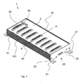
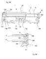
- Fig. 1 shows a schematic representation of a housing 1 for a printed circuit board 3, 3 'according to a first embodiment of the present invention in perspective view with a U - shaped housing base 10, which comprises a bottom with two opposite walls 101, 102, wherein on the housing base 10 also are attached side walls 20 which terminate the housing 1 from the side. On the side walls 20 are suitably formed feet 21, which are angled accordingly, and which allow to fix the housing 1 in a simple manner on a mounting surface.
- the cover of the housing 1 by means of a provided unfinished base surface of a printed circuit board 3, which is disposed in the housing 1, wherein the circuit board 3 may suitably also comprise sockets 30 for the connection of cables, and also may comprise a window 33 for viewing into the interior of the housing 1.
- the side walls For fixing the side walls 20 to the base body 10, the side walls comprise suitable bores 22 for corresponding fastening means.
- the upper circuit board 3 holes 34 also for suitable fastening means of the circuit board 3 to the housing base body 10th
- the housing base 10 is made of extruded profile and particularly advantageously made of extruded aluminum, so that its length can be easily changed and provided in a simple manner a variety of different variations for longer or shorter circuit boards with more or fewer connectors or outputs with sockets can be.
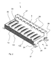
- Fig. 2 shows a perspective view of a housing 1 according to the invention for at least one printed circuit board 3, 3 'according to a further embodiment of the present invention, which in many areas of the embodiment of Fig. 1 corresponds, why the same elements of the housing 1 are provided with the same reference numerals and why, for simplicity, a further description is omitted.
- the housing 1 of Fig. 2 further comprises a mounting bracket 27 integrally formed with the side walls 20 and extending from an upwardly projecting shoulder 26 of a side wall 20 to a corresponding second protruding shoulder 26 of the second lateral wall 20 and above and in parallel to the top of the housing 1 covering printed circuit board 3 is arranged with upwardly projecting sockets 30 for connectors of cables.
- the mounting bracket 27 according to the invention comprises in particular at least one suitable row of holes provided by means of recesses 28 for fastening cable ties or cable clamps of any type for protection from connected to the sockets 30 connectors and cables and strain relief of the cable.
- the mounting bracket 27 is in particular formed integrally with the two lateral walls 2 and suitably punched from a common metal sheet, wherein the side walls 20 are angled with their feet 21 in a suitable manner.
- Fig. 2 also shows suitable fastening means 24 for fixing the side walls to the housing base body 10 and fastening means 109 for the circuit board 3, which are respectively arranged in bores, the bores 22 and 34 of the housing 1 according to the invention of the embodiment of Fig. 1 correspond.
- a side wall 20 may also suitably include a connector 25 for grounding the housing 1.
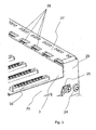
- Fig. 3 shows an enlarged perspective view of the housing 1 of the invention Fig. 1 in a partial view with the lateral wall 20; the upwardly projecting shoulder 26 and the mounting bracket 27, in which two suitably provided by means of suitable recesses 28 row of holes are provided so that a plurality of different cable ties or clamping devices are mounted on the mounting bracket 27.
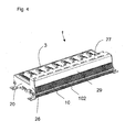
- Fig. 4 shows a schematic representation of the housing 1 according to the invention from the rear, for the sake of simplicity, only the essential basic components of the housing 1 are provided with reference numerals, namely the housing body 10 with its one wall 102, the side wall 20 and the upper circuit board 3 and the mounting bracket 27th , wherein on the mounting bracket 27 suitably and advantageously a shutter 29 is provided which is angled down to the wall 102 out and shields the area of the clamping devices and sockets 30 to the side of the wall 102 out.
- Fig. 5A shows a schematic section through the line AA of Fig. 1 with the housing 1 with its housing base 10, which is elongated and comprises a housing bottom and two lateral walls 101, 102, and with two circuit boards 3, 3 ', which are arranged in the housing 1, wherein suitably the upper circuit board 3, the housing 1 closes up and at the same time provides a connection 30 for cable.
- one of the side walls 101, 102 on its underside a suitably formed clamping zone for easy insertion and fixation of the circuit boards 3, 3 ', each with an upper and lower appropriately formed projection 106, 105; 106 ', 105' wherein each of the lower projection 105, 105 'are angled, which allows easy mounting of the circuit boards 3, 3' in the housing 1.
- the protrusions 108, 105 and 106 ', 105' are also suitably arranged such that upon insertion of a printed circuit board 3, 3 'in the space provided between the protrusions 105, 106 and 105', 106 'at an angle from above and to Lowering the circuit board 3, 3 'in a horizontal position, the circuit board 3, 3' between the projections 105,106; 105 ', 106' is held securely.
- the respective projections 106, 105; 106 ', 105' which may be suitably formed like a rail, a clamping zone for the circuit boards 3, 3 'provided.
- the opposite wall 101 includes a suitable paragraph for storage of the lower circuit board 3 ', which rests after importing the circuit board 3' in the clamping zone 105 ', 106' and after lowering the circuit board 3 'on the shoulder of the wall 101.
- the integral with the wall 101 paragraph for supporting the circuit board 3 ' suitably comprises vertical recesses 108 which correspond to the holes 34 of the circuit board 3, 3', so that suitable fasteners 109, which may be suitable and exemplary screws, the circuit board. 3 , 3 'on the housing base 10 can fix.
- a suitable spacer 110 is provided for this, which rests on the printed circuit board 3', and on which in turn rests the upper printed circuit board 3, wherein the Spacer 110 is suitably also held by the fastening means 109 and, for example, and advantageously can be sleeve-like design.
- the housing base body 10 also advantageously comprises a contour-like bottom with a contour 103 and with cooling fins 104, for dissipating or supplying heat into or out of the housing interior, wherein a suitable heat-conducting element 32 may suitably be provided in the housing interior in the vicinity of the cooling fin 104, the direct contact with the bottom of the housing base body 10 and the lower circuit board 3 'has.
- a suitable gate 23 is formed in the lateral walls 20 such that the contour 103 and the cooling fins 104 are exposed laterally.
- the housing base 10 of a housing 1 also comprises suitable horizontal recesses 108 in the walls 101, 102 for receiving fastening means 24 for fastening the lateral walls 20, wherein the fastening means 24 may suitably also be screws which engage with the recesses 108 and / or in correspond to the recesses 108 formed threaded holes.
- Fig. 5B shows an enlarged view of a portion of the schematic representation of Fig. 5A with the upper and lower circuit board 3, 3 'and the respective clamping zones 106, 105; 106 ', 105' on the inside of the wall 102, wherein advantageously in each case together with the circuit board 3, 3 'a compensation element 31 is provided on at least the bottom or the top of the circuit board 3, 3', thereby advantageously a tolerance compensation of tolerances of the strength the printed circuit board 3, 3 'is provided and also advantageously a damping of stresses and a rattle protection is provided for vibrations of the housing 1.
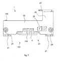
- Fig. 6 shows a perspective view of the housing 1 of the invention Fig. 2 together with a DIN rail and Fig. 7 shows a schematic side view of Fig. 6 ,
- Fig. 6 shows a perspective view of the housing 1 of the invention Fig. 2 together with a DIN rail
- Fig. 7 shows a schematic side view of Fig. 6 ,
- already described elements of the housing 1 according to the invention is dispensed with and instead to the description of the FIGS. 2 to 5 is referenced.
- an inventive housing 1 according to the second embodiment of the present invention according to Fig. 2 with the mounting bracket 27 advantageously corresponding clamping zones 105, 106; 105 ', 106' and the rest to the above description of Fig. 5 may include mentioned features.
- the advantageous contour 103 of the bottom of the housing base body 10 is formed such that the contour 103 corresponds to a DIN rail 4, and is designed to accommodate a top hat rail 4 in a simple manner, so that the housing 1 can be inserted into an existing DIN rail 4 and can be easily attached to the feet 20 on a mounting plane.
Landscapes
- Engineering & Computer Science (AREA)
- Microelectronics & Electronic Packaging (AREA)
- Mounting Of Printed Circuit Boards And The Like (AREA)
- Casings For Electric Apparatus (AREA)
Applications Claiming Priority (1)
| Application Number | Priority Date | Filing Date | Title |
|---|---|---|---|
| DE202008008516U DE202008008516U1 (de) | 2008-06-27 | 2008-06-27 | Gehäuse für Leiterplatte |
Publications (4)
| Publication Number | Publication Date |
|---|---|
| EP2139306A2 true EP2139306A2 (fr) | 2009-12-30 |
| EP2139306A3 EP2139306A3 (fr) | 2011-04-27 |
| EP2139306B1 EP2139306B1 (fr) | 2018-01-10 |
| EP2139306B8 EP2139306B8 (fr) | 2018-05-02 |
Family
ID=39768404
Family Applications (1)
| Application Number | Title | Priority Date | Filing Date |
|---|---|---|---|
| EP09100346.7A Active EP2139306B8 (fr) | 2008-06-27 | 2009-06-25 | Boîtier pour plaques conductrices |
Country Status (2)
| Country | Link |
|---|---|
| EP (1) | EP2139306B8 (fr) |
| DE (1) | DE202008008516U1 (fr) |
Cited By (1)
| Publication number | Priority date | Publication date | Assignee | Title |
|---|---|---|---|---|
| USD765613S1 (en) | 2013-04-03 | 2016-09-06 | Inter Control Hermann Kohler Elektrik Gmbh & Co. Kg | Housing for electric and electronic components |
Families Citing this family (3)
| Publication number | Priority date | Publication date | Assignee | Title |
|---|---|---|---|---|
| WO2011090223A1 (fr) * | 2010-01-21 | 2011-07-28 | 엘지전자 주식회사 | Panneau de commande pour four à micro-ondes |
| DE102012006787A1 (de) | 2012-04-04 | 2013-10-10 | Inter Control Hermann Köhler Elektrik GmbH & Co. KG | Erweiterbares Gehäuse für elektrische Bauteile, Zwischengehäuseteil für das erweiterbare Gehäuse, sowie Verfahren zur Herstellung und zur Montage des Gehäuses |
| DE102020118109A1 (de) | 2020-07-09 | 2022-01-13 | ELTEC Elektronik Aktiengesellschaft | Elektronikgehäuse |
Citations (1)
| Publication number | Priority date | Publication date | Assignee | Title |
|---|---|---|---|---|
| DE20215425U1 (de) | 2002-10-08 | 2004-02-19 | Knobel Ag Lichttechnische Komponenten | Gehäuse für eine Leiterplatte |
Family Cites Families (2)
| Publication number | Priority date | Publication date | Assignee | Title |
|---|---|---|---|---|
| US4791531A (en) * | 1987-03-09 | 1988-12-13 | Tech-S, Inc. | Extruded enclosure for electrical apparatus |
| DE102004015517B4 (de) * | 2004-03-28 | 2006-10-26 | Inter Control Hermann Köhler Elektrik GmbH & Co. KG | CAN-Knoten und Gehäuse insbesondere für CAN-Knoten |
-
2008
- 2008-06-27 DE DE202008008516U patent/DE202008008516U1/de not_active Expired - Lifetime
-
2009
- 2009-06-25 EP EP09100346.7A patent/EP2139306B8/fr active Active
Patent Citations (1)
| Publication number | Priority date | Publication date | Assignee | Title |
|---|---|---|---|---|
| DE20215425U1 (de) | 2002-10-08 | 2004-02-19 | Knobel Ag Lichttechnische Komponenten | Gehäuse für eine Leiterplatte |
Cited By (1)
| Publication number | Priority date | Publication date | Assignee | Title |
|---|---|---|---|---|
| USD765613S1 (en) | 2013-04-03 | 2016-09-06 | Inter Control Hermann Kohler Elektrik Gmbh & Co. Kg | Housing for electric and electronic components |
Also Published As
| Publication number | Publication date |
|---|---|
| EP2139306B1 (fr) | 2018-01-10 |
| DE202008008516U1 (de) | 2008-09-18 |
| EP2139306B8 (fr) | 2018-05-02 |
| EP2139306A3 (fr) | 2011-04-27 |
Similar Documents
| Publication | Publication Date | Title |
|---|---|---|
| EP2010500B1 (fr) | Dispositif de contact de semi-conducteurs de puissance sur une surface réfrigérante | |
| DE19722602C2 (de) | Wärmeableitendes Gehäuse zur Aufnahme von elektrischen oder elektronischen Bauteilen | |
| EP2915215B1 (fr) | Ensemble de modules en série pourvu d'un système de bus d'énergie | |
| DE102013218718B4 (de) | Elektrischer Anschlusskasten | |
| EP0902514B1 (fr) | Construction d'armoire pour équipements électriques ou électroniques | |
| DE102010034520A1 (de) | Träger für ein Steuergerät eines Kraftfahrzeuges, Steuergerät und Kraftfahrzeug | |
| DE102007034600B3 (de) | Montagesystem mit einer Vorrichtung zum Anordnen und Befestigen von elektrischen Einheiten, insbesodere in einem Schaltschrank | |
| DE102015103599A1 (de) | Befestigungssystem zum Montieren von Geräten, insbesondere Elektrogeräten | |
| EP2139306B1 (fr) | Boîtier pour plaques conductrices | |
| DE202004019942U1 (de) | Kabeltragvorrichtung | |
| EP1965625B1 (fr) | Support variable | |
| EP1064709B1 (fr) | Boitier d'installation a fixation murale | |
| EP3021434A1 (fr) | Dispositif et procédé pour la montage sans outil de modules sur un profilé chapeau | |
| WO2013135882A1 (fr) | Système de formation d'un panneau de distribution modulaire et procédé de montage dudit système | |
| EP0886992B1 (fr) | Chassis pour appareils electroniques | |
| WO2019072987A1 (fr) | Boîtier électronique et support de module | |
| DE102014111582B3 (de) | Computersystem sowie Haltebügel | |
| EP0596349A2 (fr) | Support pour installation électrique | |
| EP2538510B1 (fr) | Panier d'appareillage pour installations électriques souterraines | |
| DE102004059815B4 (de) | Montageträger für Unterflurdose | |
| DE29604597U1 (de) | Elektromagnetisch abgeschirmter Baugruppenträger mit variabler Befestigungsanordnung zwischen Etagenschirmblechen und Seitenwandblechen | |
| DE102004027859B4 (de) | Leiterplatte und Leiterplattenvorrichtung | |
| DE202006009561U1 (de) | Brandschutzschrank | |
| DE1813773B2 (de) | Stromleiste zur Verlegung einer elektrischen Installation | |
| DE102023202592A1 (de) | Verteilerschrank mit hoher Schutzart und Herstellverfahren |
Legal Events
| Date | Code | Title | Description |
|---|---|---|---|
| PUAI | Public reference made under article 153(3) epc to a published international application that has entered the european phase |
Free format text: ORIGINAL CODE: 0009012 |
|
| AK | Designated contracting states |
Kind code of ref document: A2 Designated state(s): AT BE BG CH CY CZ DE DK EE ES FI FR GB GR HR HU IE IS IT LI LT LU LV MC MK MT NL NO PL PT RO SE SI SK TR |
|
| PUAL | Search report despatched |
Free format text: ORIGINAL CODE: 0009013 |
|
| AK | Designated contracting states |
Kind code of ref document: A3 Designated state(s): AT BE BG CH CY CZ DE DK EE ES FI FR GB GR HR HU IE IS IT LI LT LU LV MC MK MT NL NO PL PT RO SE SI SK TR |
|
| AX | Request for extension of the european patent |
Extension state: AL BA RS |
|
| 17P | Request for examination filed |
Effective date: 20111021 |
|
| 17Q | First examination report despatched |
Effective date: 20150402 |
|
| GRAP | Despatch of communication of intention to grant a patent |
Free format text: ORIGINAL CODE: EPIDOSNIGR1 |
|
| INTG | Intention to grant announced |
Effective date: 20170929 |
|
| GRAS | Grant fee paid |
Free format text: ORIGINAL CODE: EPIDOSNIGR3 |
|
| GRAA | (expected) grant |
Free format text: ORIGINAL CODE: 0009210 |
|
| AK | Designated contracting states |
Kind code of ref document: B1 Designated state(s): AT BE BG CH CY CZ DE DK EE ES FI FR GB GR HR HU IE IS IT LI LT LU LV MC MK MT NL NO PL PT RO SE SI SK TR |
|
| REG | Reference to a national code |
Ref country code: GB Ref legal event code: FG4D Free format text: NOT ENGLISH |
|
| REG | Reference to a national code |
Ref country code: CH Ref legal event code: EP Ref country code: AT Ref legal event code: REF Ref document number: 963789 Country of ref document: AT Kind code of ref document: T Effective date: 20180115 |
|
| REG | Reference to a national code |
Ref country code: IE Ref legal event code: FG4D Free format text: LANGUAGE OF EP DOCUMENT: GERMAN |
|
| REG | Reference to a national code |
Ref country code: DE Ref legal event code: R096 Ref document number: 502009014661 Country of ref document: DE |
|
| REG | Reference to a national code |
Ref country code: DE Ref legal event code: R082 Ref document number: 502009014661 Country of ref document: DE Representative=s name: STIPPL PATENTANWAELTE, DE Ref country code: DE Ref legal event code: R081 Ref document number: 502009014661 Country of ref document: DE Owner name: INTER CONTROL HERMANN KOEHLER ELEKTRIK GMBH & , DE Free format text: FORMER OWNER: INTER CONTROL HERMANN KOEHLER GMBH & CO. KG, 90411 NUERNBERG, DE |
|
| GRAT | Correction requested after decision to grant or after decision to maintain patent in amended form |
Free format text: ORIGINAL CODE: EPIDOSNCDEC |
|
| REG | Reference to a national code |
Ref country code: CH Ref legal event code: NV Representative=s name: PATENTANWAELTE SCHAAD, BALASS, MENZL AND PARTN, CH Ref country code: CH Ref legal event code: PK Free format text: BERICHTIGUNG INHABER |
|
| RAP2 | Party data changed (patent owner data changed or rights of a patent transferred) |
Owner name: INTER CONTROL HERMANN KOEHLER ELEKTRIK GMBH & CO., |
|
| REG | Reference to a national code |
Ref country code: GB Ref legal event code: S117 Free format text: REQUEST FILED; REQUEST FOR CORRECTION UNDER SECTION 117 FILED ON 07 MARCH 2018 |
|
| REG | Reference to a national code |
Ref country code: GB Ref legal event code: S117 Free format text: CORRECTIONS ALLOWED; REQUEST FOR CORRECTION UNDER SECTION 117 FILED ON 07 MARCH 2018 ALLOWED ON 16 APRIL 2018 |
|
| REG | Reference to a national code |
Ref country code: NL Ref legal event code: MP Effective date: 20180110 |
|
| REG | Reference to a national code |
Ref country code: FR Ref legal event code: PLFP Year of fee payment: 10 |
|
| PG25 | Lapsed in a contracting state [announced via postgrant information from national office to epo] |
Ref country code: NL Free format text: LAPSE BECAUSE OF FAILURE TO SUBMIT A TRANSLATION OF THE DESCRIPTION OR TO PAY THE FEE WITHIN THE PRESCRIBED TIME-LIMIT Effective date: 20180110 |
|
| PG25 | Lapsed in a contracting state [announced via postgrant information from national office to epo] |
Ref country code: ES Free format text: LAPSE BECAUSE OF FAILURE TO SUBMIT A TRANSLATION OF THE DESCRIPTION OR TO PAY THE FEE WITHIN THE PRESCRIBED TIME-LIMIT Effective date: 20180110 Ref country code: LT Free format text: LAPSE BECAUSE OF FAILURE TO SUBMIT A TRANSLATION OF THE DESCRIPTION OR TO PAY THE FEE WITHIN THE PRESCRIBED TIME-LIMIT Effective date: 20180110 Ref country code: NO Free format text: LAPSE BECAUSE OF FAILURE TO SUBMIT A TRANSLATION OF THE DESCRIPTION OR TO PAY THE FEE WITHIN THE PRESCRIBED TIME-LIMIT Effective date: 20180410 Ref country code: HR Free format text: LAPSE BECAUSE OF FAILURE TO SUBMIT A TRANSLATION OF THE DESCRIPTION OR TO PAY THE FEE WITHIN THE PRESCRIBED TIME-LIMIT Effective date: 20180110 Ref country code: CY Free format text: LAPSE BECAUSE OF FAILURE TO SUBMIT A TRANSLATION OF THE DESCRIPTION OR TO PAY THE FEE WITHIN THE PRESCRIBED TIME-LIMIT Effective date: 20180110 |
|
| PG25 | Lapsed in a contracting state [announced via postgrant information from national office to epo] |
Ref country code: PL Free format text: LAPSE BECAUSE OF FAILURE TO SUBMIT A TRANSLATION OF THE DESCRIPTION OR TO PAY THE FEE WITHIN THE PRESCRIBED TIME-LIMIT Effective date: 20180110 Ref country code: IS Free format text: LAPSE BECAUSE OF FAILURE TO SUBMIT A TRANSLATION OF THE DESCRIPTION OR TO PAY THE FEE WITHIN THE PRESCRIBED TIME-LIMIT Effective date: 20180510 Ref country code: LV Free format text: LAPSE BECAUSE OF FAILURE TO SUBMIT A TRANSLATION OF THE DESCRIPTION OR TO PAY THE FEE WITHIN THE PRESCRIBED TIME-LIMIT Effective date: 20180110 Ref country code: SE Free format text: LAPSE BECAUSE OF FAILURE TO SUBMIT A TRANSLATION OF THE DESCRIPTION OR TO PAY THE FEE WITHIN THE PRESCRIBED TIME-LIMIT Effective date: 20180110 Ref country code: GR Free format text: LAPSE BECAUSE OF FAILURE TO SUBMIT A TRANSLATION OF THE DESCRIPTION OR TO PAY THE FEE WITHIN THE PRESCRIBED TIME-LIMIT Effective date: 20180411 Ref country code: BG Free format text: LAPSE BECAUSE OF FAILURE TO SUBMIT A TRANSLATION OF THE DESCRIPTION OR TO PAY THE FEE WITHIN THE PRESCRIBED TIME-LIMIT Effective date: 20180410 |
|
| PG25 | Lapsed in a contracting state [announced via postgrant information from national office to epo] |
Ref country code: MT Free format text: LAPSE BECAUSE OF FAILURE TO SUBMIT A TRANSLATION OF THE DESCRIPTION OR TO PAY THE FEE WITHIN THE PRESCRIBED TIME-LIMIT Effective date: 20180110 |
|
| REG | Reference to a national code |
Ref country code: DE Ref legal event code: R097 Ref document number: 502009014661 Country of ref document: DE |
|
| PG25 | Lapsed in a contracting state [announced via postgrant information from national office to epo] |
Ref country code: IT Free format text: LAPSE BECAUSE OF FAILURE TO SUBMIT A TRANSLATION OF THE DESCRIPTION OR TO PAY THE FEE WITHIN THE PRESCRIBED TIME-LIMIT Effective date: 20180110 Ref country code: EE Free format text: LAPSE BECAUSE OF FAILURE TO SUBMIT A TRANSLATION OF THE DESCRIPTION OR TO PAY THE FEE WITHIN THE PRESCRIBED TIME-LIMIT Effective date: 20180110 Ref country code: RO Free format text: LAPSE BECAUSE OF FAILURE TO SUBMIT A TRANSLATION OF THE DESCRIPTION OR TO PAY THE FEE WITHIN THE PRESCRIBED TIME-LIMIT Effective date: 20180110 |
|
| PLBE | No opposition filed within time limit |
Free format text: ORIGINAL CODE: 0009261 |
|
| STAA | Information on the status of an ep patent application or granted ep patent |
Free format text: STATUS: NO OPPOSITION FILED WITHIN TIME LIMIT |
|
| PG25 | Lapsed in a contracting state [announced via postgrant information from national office to epo] |
Ref country code: CZ Free format text: LAPSE BECAUSE OF FAILURE TO SUBMIT A TRANSLATION OF THE DESCRIPTION OR TO PAY THE FEE WITHIN THE PRESCRIBED TIME-LIMIT Effective date: 20180110 Ref country code: SK Free format text: LAPSE BECAUSE OF FAILURE TO SUBMIT A TRANSLATION OF THE DESCRIPTION OR TO PAY THE FEE WITHIN THE PRESCRIBED TIME-LIMIT Effective date: 20180110 Ref country code: DK Free format text: LAPSE BECAUSE OF FAILURE TO SUBMIT A TRANSLATION OF THE DESCRIPTION OR TO PAY THE FEE WITHIN THE PRESCRIBED TIME-LIMIT Effective date: 20180110 |
|
| 26N | No opposition filed |
Effective date: 20181011 |
|
| PG25 | Lapsed in a contracting state [announced via postgrant information from national office to epo] |
Ref country code: FI Free format text: LAPSE BECAUSE OF NON-PAYMENT OF DUE FEES Effective date: 20180625 |
|
| REG | Reference to a national code |
Ref country code: CH Ref legal event code: PL |
|
| PG25 | Lapsed in a contracting state [announced via postgrant information from national office to epo] |
Ref country code: SI Free format text: LAPSE BECAUSE OF FAILURE TO SUBMIT A TRANSLATION OF THE DESCRIPTION OR TO PAY THE FEE WITHIN THE PRESCRIBED TIME-LIMIT Effective date: 20180110 |
|
| REG | Reference to a national code |
Ref country code: BE Ref legal event code: MM Effective date: 20180630 |
|
| REG | Reference to a national code |
Ref country code: IE Ref legal event code: MM4A |
|
| PG25 | Lapsed in a contracting state [announced via postgrant information from national office to epo] |
Ref country code: MC Free format text: LAPSE BECAUSE OF FAILURE TO SUBMIT A TRANSLATION OF THE DESCRIPTION OR TO PAY THE FEE WITHIN THE PRESCRIBED TIME-LIMIT Effective date: 20180110 Ref country code: LU Free format text: LAPSE BECAUSE OF NON-PAYMENT OF DUE FEES Effective date: 20180625 |
|
| PG25 | Lapsed in a contracting state [announced via postgrant information from national office to epo] |
Ref country code: IE Free format text: LAPSE BECAUSE OF NON-PAYMENT OF DUE FEES Effective date: 20180625 Ref country code: CH Free format text: LAPSE BECAUSE OF NON-PAYMENT OF DUE FEES Effective date: 20180630 Ref country code: LI Free format text: LAPSE BECAUSE OF NON-PAYMENT OF DUE FEES Effective date: 20180630 |
|
| PG25 | Lapsed in a contracting state [announced via postgrant information from national office to epo] |
Ref country code: BE Free format text: LAPSE BECAUSE OF NON-PAYMENT OF DUE FEES Effective date: 20180630 |
|
| REG | Reference to a national code |
Ref country code: AT Ref legal event code: MM01 Ref document number: 963789 Country of ref document: AT Kind code of ref document: T Effective date: 20180625 |
|
| PG25 | Lapsed in a contracting state [announced via postgrant information from national office to epo] |
Ref country code: AT Free format text: LAPSE BECAUSE OF NON-PAYMENT OF DUE FEES Effective date: 20180625 |
|
| PG25 | Lapsed in a contracting state [announced via postgrant information from national office to epo] |
Ref country code: TR Free format text: LAPSE BECAUSE OF FAILURE TO SUBMIT A TRANSLATION OF THE DESCRIPTION OR TO PAY THE FEE WITHIN THE PRESCRIBED TIME-LIMIT Effective date: 20180110 |
|
| PG25 | Lapsed in a contracting state [announced via postgrant information from national office to epo] |
Ref country code: PT Free format text: LAPSE BECAUSE OF FAILURE TO SUBMIT A TRANSLATION OF THE DESCRIPTION OR TO PAY THE FEE WITHIN THE PRESCRIBED TIME-LIMIT Effective date: 20180110 Ref country code: HU Free format text: LAPSE BECAUSE OF FAILURE TO SUBMIT A TRANSLATION OF THE DESCRIPTION OR TO PAY THE FEE WITHIN THE PRESCRIBED TIME-LIMIT; INVALID AB INITIO Effective date: 20090625 |
|
| PG25 | Lapsed in a contracting state [announced via postgrant information from national office to epo] |
Ref country code: MK Free format text: LAPSE BECAUSE OF NON-PAYMENT OF DUE FEES Effective date: 20180110 |
|
| P01 | Opt-out of the competence of the unified patent court (upc) registered |
Effective date: 20230508 |
|
| PGFP | Annual fee paid to national office [announced via postgrant information from national office to epo] |
Ref country code: GB Payment date: 20230622 Year of fee payment: 15 |
|
| REG | Reference to a national code |
Ref country code: DE Ref legal event code: R082 Ref document number: 502009014661 Country of ref document: DE Representative=s name: 4IP GLEIMPETRI PATENT- UND RECHTSANWALTSPARTNE, DE |
|
| GBPC | Gb: european patent ceased through non-payment of renewal fee |
Effective date: 20240625 |
|
| PG25 | Lapsed in a contracting state [announced via postgrant information from national office to epo] |
Ref country code: GB Free format text: LAPSE BECAUSE OF NON-PAYMENT OF DUE FEES Effective date: 20240625 |
|
| PGFP | Annual fee paid to national office [announced via postgrant information from national office to epo] |
Ref country code: DE Payment date: 20250312 Year of fee payment: 17 |
|
| PGFP | Annual fee paid to national office [announced via postgrant information from national office to epo] |
Ref country code: FR Payment date: 20250626 Year of fee payment: 17 |