EP2127029B1 - Anschlussklemmleiste - Google Patents
Anschlussklemmleiste Download PDFInfo
- Publication number
- EP2127029B1 EP2127029B1 EP07856677.5A EP07856677A EP2127029B1 EP 2127029 B1 EP2127029 B1 EP 2127029B1 EP 07856677 A EP07856677 A EP 07856677A EP 2127029 B1 EP2127029 B1 EP 2127029B1
- Authority
- EP
- European Patent Office
- Prior art keywords
- insulation displacement
- displacement contacts
- contacts
- housing
- terminal block
- Prior art date
- Legal status (The legal status is an assumption and is not a legal conclusion. Google has not performed a legal analysis and makes no representation as to the accuracy of the status listed.)
- Active
Links
- 238000006073 displacement reaction Methods 0.000 claims description 99
- 238000009413 insulation Methods 0.000 claims description 99
- 101000729843 Loxosceles cf. spinulosa (strain GJB-2008) Dermonecrotic toxin LcsSicTox-betaIC1 Proteins 0.000 claims description 4
- 230000008878 coupling Effects 0.000 description 2
- 238000010168 coupling process Methods 0.000 description 2
- 238000005859 coupling reaction Methods 0.000 description 2
- 239000003990 capacitor Substances 0.000 description 1
- 230000001419 dependent effect Effects 0.000 description 1
- 230000000994 depressogenic effect Effects 0.000 description 1
Images

Classifications
-
- H—ELECTRICITY
- H01—ELECTRIC ELEMENTS
- H01R—ELECTRICALLY-CONDUCTIVE CONNECTIONS; STRUCTURAL ASSOCIATIONS OF A PLURALITY OF MUTUALLY-INSULATED ELECTRICAL CONNECTING ELEMENTS; COUPLING DEVICES; CURRENT COLLECTORS
- H01R4/00—Electrically-conductive connections between two or more conductive members in direct contact, i.e. touching one another; Means for effecting or maintaining such contact; Electrically-conductive connections having two or more spaced connecting locations for conductors and using contact members penetrating insulation
- H01R4/24—Connections using contact members penetrating or cutting insulation or cable strands
- H01R4/2416—Connections using contact members penetrating or cutting insulation or cable strands the contact members having insulation-cutting edges, e.g. of tuning fork type
- H01R4/242—Connections using contact members penetrating or cutting insulation or cable strands the contact members having insulation-cutting edges, e.g. of tuning fork type the contact members being plates having a single slot
- H01R4/2425—Flat plates, e.g. multi-layered flat plates
- H01R4/2429—Flat plates, e.g. multi-layered flat plates mounted in an insulating base
-
- H—ELECTRICITY
- H01—ELECTRIC ELEMENTS
- H01R—ELECTRICALLY-CONDUCTIVE CONNECTIONS; STRUCTURAL ASSOCIATIONS OF A PLURALITY OF MUTUALLY-INSULATED ELECTRICAL CONNECTING ELEMENTS; COUPLING DEVICES; CURRENT COLLECTORS
- H01R12/00—Structural associations of a plurality of mutually-insulated electrical connecting elements, specially adapted for printed circuits, e.g. printed circuit boards [PCB], flat or ribbon cables, or like generally planar structures, e.g. terminal strips, terminal blocks; Coupling devices specially adapted for printed circuits, flat or ribbon cables, or like generally planar structures; Terminals specially adapted for contact with, or insertion into, printed circuits, flat or ribbon cables, or like generally planar structures
- H01R12/50—Fixed connections
- H01R12/51—Fixed connections for rigid printed circuits or like structures
- H01R12/515—Terminal blocks providing connections to wires or cables
-
- H—ELECTRICITY
- H01—ELECTRIC ELEMENTS
- H01R—ELECTRICALLY-CONDUCTIVE CONNECTIONS; STRUCTURAL ASSOCIATIONS OF A PLURALITY OF MUTUALLY-INSULATED ELECTRICAL CONNECTING ELEMENTS; COUPLING DEVICES; CURRENT COLLECTORS
- H01R12/00—Structural associations of a plurality of mutually-insulated electrical connecting elements, specially adapted for printed circuits, e.g. printed circuit boards [PCB], flat or ribbon cables, or like generally planar structures, e.g. terminal strips, terminal blocks; Coupling devices specially adapted for printed circuits, flat or ribbon cables, or like generally planar structures; Terminals specially adapted for contact with, or insertion into, printed circuits, flat or ribbon cables, or like generally planar structures
- H01R12/70—Coupling devices
- H01R12/71—Coupling devices for rigid printing circuits or like structures
- H01R12/72—Coupling devices for rigid printing circuits or like structures coupling with the edge of the rigid printed circuits or like structures
- H01R12/722—Coupling devices for rigid printing circuits or like structures coupling with the edge of the rigid printed circuits or like structures coupling devices mounted on the edge of the printed circuits
- H01R12/724—Coupling devices for rigid printing circuits or like structures coupling with the edge of the rigid printed circuits or like structures coupling devices mounted on the edge of the printed circuits containing contact members forming a right angle
-
- H—ELECTRICITY
- H01—ELECTRIC ELEMENTS
- H01R—ELECTRICALLY-CONDUCTIVE CONNECTIONS; STRUCTURAL ASSOCIATIONS OF A PLURALITY OF MUTUALLY-INSULATED ELECTRICAL CONNECTING ELEMENTS; COUPLING DEVICES; CURRENT COLLECTORS
- H01R13/00—Details of coupling devices of the kinds covered by groups H01R12/70 or H01R24/00 - H01R33/00
- H01R13/646—Details of coupling devices of the kinds covered by groups H01R12/70 or H01R24/00 - H01R33/00 specially adapted for high-frequency, e.g. structures providing an impedance match or phase match
- H01R13/6473—Impedance matching
- H01R13/6477—Impedance matching by variation of dielectric properties
-
- H—ELECTRICITY
- H01—ELECTRIC ELEMENTS
- H01R—ELECTRICALLY-CONDUCTIVE CONNECTIONS; STRUCTURAL ASSOCIATIONS OF A PLURALITY OF MUTUALLY-INSULATED ELECTRICAL CONNECTING ELEMENTS; COUPLING DEVICES; CURRENT COLLECTORS
- H01R13/00—Details of coupling devices of the kinds covered by groups H01R12/70 or H01R24/00 - H01R33/00
- H01R13/646—Details of coupling devices of the kinds covered by groups H01R12/70 or H01R24/00 - H01R33/00 specially adapted for high-frequency, e.g. structures providing an impedance match or phase match
- H01R13/6461—Means for preventing cross-talk
- H01R13/6467—Means for preventing cross-talk by cross-over of signal conductors
-
- H—ELECTRICITY
- H01—ELECTRIC ELEMENTS
- H01R—ELECTRICALLY-CONDUCTIVE CONNECTIONS; STRUCTURAL ASSOCIATIONS OF A PLURALITY OF MUTUALLY-INSULATED ELECTRICAL CONNECTING ELEMENTS; COUPLING DEVICES; CURRENT COLLECTORS
- H01R24/00—Two-part coupling devices, or either of their cooperating parts, characterised by their overall structure
- H01R24/60—Contacts spaced along planar side wall transverse to longitudinal axis of engagement
- H01R24/62—Sliding engagements with one side only, e.g. modular jack coupling devices
- H01R24/64—Sliding engagements with one side only, e.g. modular jack coupling devices for high frequency, e.g. RJ 45
-
- H—ELECTRICITY
- H04—ELECTRIC COMMUNICATION TECHNIQUE
- H04Q—SELECTING
- H04Q1/00—Details of selecting apparatus or arrangements
- H04Q1/02—Constructional details
- H04Q1/14—Distribution frames
- H04Q1/148—Identification strips for distribution frames
Definitions
- the invention relates to a terminal strip according to the preamble of claim 1.
- a terminal block is for example from the DE 102 57 308 B3 known.
- the terminal strip is designed as a connector for printed circuit boards, comprising a number of contact elements, wherein the contact elements each have two terminal sides, wherein one terminal side as insulation displacement contact for connecting wires and the other terminal side as a fork contact for contacting pads is formed on a circuit board, and a plastic housing into which the insulation displacement contacts of the contact elements are inserted, wherein the insulation displacement contact and the fork contact are arranged rotated to each other and at least one lower edge of the insulation displacement contact on the plastic housing supported, so that the contact elements are held captive in occurring occurring Anschalt originallyn on the insulation displacement contacts in the plastic housing.
- the insulation displacement contacts lie between housing walls, wherein the insulation displacement contacts are aligned at an angle of 45 ° to the housing walls, wherein the insulation displacement contacts of the series are all aligned parallel to each other.
- a terminal strip comprising a housing and at least four insulation displacement contacts, wherein the at least four insulation displacement contacts are arranged in a row, the housing is formed with housing walls, between which the insulation displacement contacts are arranged, wherein the insulation displacement contacts are aligned at an angle of 45 ° to the housing walls and in each case two insulation displacement contacts form a contact pair, wherein the insulation displacement contacts of a pair of contacts aligned parallel to each other whereas adjacent insulation displacement contacts of different pairs of contacts are rotated 90 ° about the longitudinal axis of the insulation displacement contacts and the insulation displacement contacts are connected to a circuit board.
- a terminal strip comprising a housing and at least four insulation displacement contacts, wherein the at least four insulation displacement contacts are arranged in a row, the housing is formed with housing walls, between which the insulation displacement contacts are arranged, wherein the insulation displacement contacts are aligned at an angle of 45 ° to the housing walls and in each case two insulation displacement contacts form a pair of contacts, wherein the insulation displacement contacts of a contact pair are aligned parallel to each other, whereas adjacent insulation displacement Contacts of different contact pairs are arranged rotated by 90 ° about the longitudinal axis of the insulation displacement contacts to each other.
- the terminal block includes at least one further row of insulation displacement contacts arranged in parallel with the first row of insulation displacement contacts, with opposed insulation displacement contacts of different rows 90 ° about the longitudinal axis of the insulation displacement contacts are arranged rotated to each other.
- the distance between the rows is greater than the largest distance between two adjacent insulation displacement contacts of a row.
- a terminal block comprising a housing and at least four insulation displacement contacts, wherein the at least four insulation displacement contacts are arranged in a row, the housing is formed with housing walls, between which the insulation displacement contacts at an angle are aligned by 45 ° to the housing walls and each two insulation displacement contacts form a contact pair.
- the housing walls between insulation displacement contacts of a pair of contacts a smaller width than the housing walls between insulation displacement contacts of different pairs of contacts.
- a terminal strip comprising two rows of insulation displacement contacts, the longitudinal axes of the insulation displacement contacts are aligned parallel to the surface of a circuit board to which the insulation displacement contacts are connected.
- the invention is based on the technical problem of providing a terminal strip with better crosstalk behavior.
- the terminal strip comprises a housing and at least four insulation displacement contacts, wherein the at least four insulation displacement contacts are arranged in a row, the housing is formed with housing walls, between which the insulation displacement contacts are arranged, wherein the Cutting-clamp contacts are aligned at an angle of 45 ° to the housing walls and each two insulation displacement contacts form a contact pair, wherein the insulation displacement contacts of a contact pair are aligned parallel to each other, whereas adjacent insulation displacement contacts different Contact pairs are arranged rotated by 90 ° about the longitudinal axis of the insulation displacement contacts to each other.
- the capacitive coupling between contacts of adjacent contact pairs is reduced, which leads to a reduction of crosstalk.
- the two adjacent contacts form a plate capacitor, wherein the distance by the opposite direction of inclination is continuous increases, which reduces the capacity.
- the angle of 45 ° due to the tolerances of the housing can vary by +/- 5 °.
- the insulation displacement contacts are connected to a printed circuit board, wherein at least one contact pair is crossed before the connection to the printed circuit board.
- the housing walls between insulation displacement contacts of a contact pair have a smaller width than the housing walls between insulation displacement contacts of different contact pairs. This also reduces the capacitive coupling.
- the terminal strip comprises at least one further row of insulation displacement contacts arranged parallel to the first row of insulation displacement contacts, with opposed insulation displacement contacts of different rows being 90 ° about the longitudinal axis of the cutting Clamp contacts are rotated to each other. This also reduces crosstalk.
- the distance between the rows is greater than the maximum distance between two adjacent insulation displacement contacts of a row.
- the distance is preferably selected such that the insulation displacement contacts can be connected to standard attachment tools.
- the longitudinal axes of the insulation displacement contacts are aligned parallel to the surface of the circuit board.
- the insulation displacement contacts are connected to the printed circuit board via SMD-like contacts.
- the terminal strip 1 comprises a housing 2 with two rows 3, 4 of insulation displacement contacts K1-K8.
- the row 3 includes the insulation displacement contacts K1, K2, K7 and K8, wherein each of the insulation displacement contacts K1, K2 and K7, K8 form a contact pair.
- the row 4 of the insulation displacement contacts K3-K6 formed, wherein the insulation displacement contacts K3, K6 and K4, K5 form a contact pair.
- the two rows 3, 4 are formed parallel to each other.
- the rows 3, 4 comprise different housing walls 5, between which the insulation displacement contacts K1-K8 are arranged, wherein the insulation displacement contacts K1-K8 are set at an angle of 45 ° to the housing walls 5. In this case, the insulation displacement contacts K1, K2 are aligned parallel to each other.
- the insulation displacement contacts K7, K8; K3, K6 and K4, K5, each forming a contact pair Neighboring insulation displacement contacts, which are arranged in a common row 3, 4, but belonging to different pairs of contacts, so for example the insulation displacement contacts K1, K8 in row 3 or the insulation displacement contacts K5, K6 in series 4, are arranged rotated by 90 ° about the longitudinal axis of the insulation displacement contacts to each other.
- the longitudinal axis is an axis that would pierce the paper plane perpendicular.
- the distance b between the insulation displacement contacts of a contact pair is smaller than the distance c between adjacent insulation displacement contacts of different pairs of contacts, wherein the width of the housing walls 5 is referred to as the distance.
- the distance a of the row 3 and 4 to each other is greater than the distance c.
- opposing insulation displacement contacts of different rows for example, the insulation displacement contacts K2 and K3, are also arranged rotated by 90 ° about the longitudinal axis of the insulation displacement contacts to each other.
- nubs 6 are arranged on the inner sides of the housing walls, which serve to hold the depressed in the insulation displacement contacts wires.
- a preferred embodiment for connecting the insulation displacement contacts K1-K8 is shown to a circuit board 7.
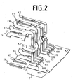
- the insulation displacement contacts K1-K8 are formed at their opposite ends with SMD-like contacts K11-K18, which are preferably soldered on the surface of the circuit board 7.
- the insulation displacement contacts K1 and K2 as well as K7 and K8 are crossed on their way to the printed circuit board 7, thereby compensating for the increased crosstalk due to the longer connecting pieces between the insulation displacement contacts and the SMD -like contacts arises.
Landscapes
- Coupling Device And Connection With Printed Circuit (AREA)
- Details Of Connecting Devices For Male And Female Coupling (AREA)
Description
- Die Erfindung betrifft eine Anschlussklemmleiste gemäß dem Oberbegriff des Anspruchs 1.
- Eine Anschlussklemmleiste ist beispielsweise aus der
DE 102 57 308 B3 bekannt. Die Anschlussklemmleiste ist dabei als Steckverbinder für Leiterplatten ausgebildet, umfassend eine Anzahl von Kontaktelementen, wobei die Kontaktelemente jeweils zwei Anschlussseiten aufweisen, wobei die eine Anschlussseite als Schneid-Klemm-Kontakt zum Anschließen von Adern und die andere Anschlussseite als Gabel-Kontakt zum Kontaktieren von Anschlussflächen auf einer Leiterplatte ausgebildet ist, und ein Kunststoffgehäuse, in das die Schneid-Klemm-Kontakte der Kontaktelemente einsteckbar sind, wobei der Schneid-Klemm-Kontakt und der Gabelkontakt zueinander verdreht angeordnet sind und mindestens eine Unterkante des Schneid-Klemm-Kontaktes sich am Kunststoffgehäuse abstützt, so dass die Kontaktelemente bei auftretenden Anschaltkräften auf die Schneid-Klemm-Kontakte verliersicher in dem Kunststoffgehäuse gehalten werden. Die Schneid-Klemm-Kontakte liegen dabei zwischen Gehäusewänden, wobei die Schneid-Klemm-Kontakte in einem Winkel von 45° zu den Gehäusewänden ausgerichtet sind, wobei die Schneid-Klemm-Kontakte der Reihe alle parallel zueinander ausgerichtet sind. - Aus der
WO 2006/053436 A1 sowie derWO 2005/064755 A1 ist eine Anschlussklemmleiste bekannt, umfassend ein Gehäuse und mindestens vier Schneid-Klemm-Kontakte, wobei die mindestens vier Schneid-Klemm-Kontakte in einer Reihe angeordnet sind, das Gehäuse mit Gehäusewänden ausgebildet ist, zwischen denen die Schneid-Klemm-Kontakte angeordnet sind, wobei die Schneid-Klemm-Kontakte in einem Winkel von 45° zu den Gehäusewänden ausgerichtet sind und jeweils zwei Schneid-Klemm-Kontakte ein Kontaktpaar bilden, wobei die Schneid-Klemm-Kontakte eines Kontaktpaares zueinander parallel ausgerichtet sind, wohingegen benachbarte Schneid-Klemm-Kontakte verschiedener Kontaktpaare um 90° um die Längsachse der Schneid-Klemm-Kontakte gedreht zueinander angeordnet sind und die Schneid-Klemm-Kontakte mit einer Leiterplatte verbunden sind. - Aus der
EP 0 899 823 A2 ist eine Anschlussklemmleiste bekannt, umfassend ein Gehäuse und mindestens vier Schneid-Klemm-Kontakte, wobei die mindestens vier Schneid-Klemm-Kontakte in einer Reihe angeordnet sind, das Gehäuse mit Gehäusewänden ausgebildet ist, zwischen denen die Schneid-Klemm-Kontakte angeordnet sind, wobei die Schneid-Klemm-Kontakte in einem Winkel von 45° zu den Gehäusewänden ausgerichtet sind und jeweils zwei Schneid-Klemm-Kontakte ein Kontaktpaar bilden, wobei die Schneid-Klemm-Kontakte eines Kontaktpaares zueinander parallel ausgerichtet sind, wohingegen benachbarte Schneid-Klemm-Kontakte verschiedener Kontaktpaare um 90° um die Längsachse der Schneid-Klemm-Kontakte gedreht zueinander angeordnet sind. Weiter umfasst die Anschlussklemmleiste mindestens eine weitere Reihe von Schneid-Klemm-Kontakten, die parallel zur ersten Reihe der Schneid-Klemm-Kontakte angeordnet ist, wobei gegenüberliegende Schneid-Klemm-Kontakte unterschiedlicher Reihen um 90° um die Längsachse der Schneid-Klemm-Kontakte gedreht zueinander angeordnet sind. Dabei ist der Abstand der Reihen zueinander größer als der größte Abstand zwischen zwei benachbarten Schneid-Klemm-Kontakten einer Reihe. - Aus der
US 6,213,809 B1 ist eine Anschlussklemmleiste bekannt, umfassend ein Gehäuse und mindestens vier Schneid-Klemm-Kontakte, wobei die mindestens vier Schneid-Klemm-Kontakte in einer Reihe angeordnet sind, das Gehäuse mit Gehäusewänden ausgebildet ist, zwischen denen die Schneid-Klemm-Kontakte in einem Winkel von 45° zu den Gehäusewänden ausgerichtet sind und jeweils zwei Schneid-Klemm-Kontakte ein Kontaktpaar bilden. Dabei weisen die Gehäusewände zwischen Schneid-Klemm-Kontakten eines Kontaktpaares eine geringere Breite auf als die Gehäusewände zwischen Schneid-Klemm-Kontakten verschiedener Kontaktpaare. - Aus der
EP 1 622 234 A1 ist eine Anschlussklemmleiste bekannt, umfassend zwei Reihen von Schneid-Klemm-Kontakten, wobei die Längsachsen der Schneid-Klemm-Kontakte parallel zur Oberfläche einer Leiterplatte ausgerichtet sind, mit der die Schneid-Klemm-Kontakte verbunden sind. - Der Erfindung liegt das technische Problem zugrunde, eine Anschlussklemmleiste mit besserem Übersprechverhalten zu schaffen.
- Die Lösung des technischen Problems ergibt sich durch den Gegenstand mit den Merkmalen des Anspruchs 1. Weitere vorteilhafte Ausgestaltungen der Erfindung ergeben sich aus den Unteransprüchen.
- Hierzu umfasst die Anschlussklemmleiste ein Gehäuse und mindestens vier Schneid-Klemm-Kontakte, wobei die mindestens vier Schneid-Klemm-Kontakte in einer Reihe angeordnet sind, das Gehäuse mit Gehäusewänden ausgebildet ist, zwischen denen die Schneid-Klemm-Kontakte angeordnet sind, wobei die Schneid-Klemm-Kontakte in einem Winkel von 45° zu den Gehäusewänden ausgerichtet sind und jeweils zwei Schneid-Klemm-Kontakte ein Kontaktpaar bilden, wobei die Schneid-Klemm-Kontakte eines Kontaktpaares zueinander parallel ausgerichtet sind, wohingegen benachbarte Schneid-Klemm-Kontakte verschiedener Kontaktpaare um 90° um die Längsachse der Schneid-Klemm-Kontakte gedreht zueinander angeordnet sind. Hierdurch wird die kapazitive Kopplung zwischen Kontakten benachbarter Kontaktpaare reduziert, was zu einer Reduzierung des Übersprechens führt. Anschaulich bilden die beiden benachbarten Kontakte einen Plattenkondensator, wobei der Abstand durch die gegensinnige Schrägstellung sich kontinuierlich vergrößert, was die Kapazität verkleinert. Dabei sei angemerkt, dass der Winkel von 45° aufgrund der Toleranzen des Gehäuses um +/- 5° schwanken kann. Dabei sind die Schneid-Klemm-Kontakte mit einer Leiterplatte verbunden, wobei mindestens ein Kontaktpaar vor der Verbindung mit der Leiterplatte gekreuzt ist.
- In einer bevorzugten Ausführungsform weisen die Gehäusewände zwischen Schneid-Klemm-Kontakten eines Kontaktpaares eine geringere Breite auf als die Gehäusewände zwischen Schneid-Klemm-Kontakten verschiedener Kontaktpaare. Auch hierdurch wird die kapazitive Kopplung reduziert.
- In einer weiteren bevorzugten Ausführungsform umfasst die Anschlussklemmleiste mindestens eine weitere Reihe von Schneid-Klemm-Kontakten, die parallel zur ersten Reihe der Schneid-Klemm-Kontakte angeordnet ist, wobei gegenüberliegende Schneid-Klemm-Kontakte unterschiedlicher Reihen um 90° um die Längsachse der Schneid-Klemm-Kontakte gedreht zueinander angeordnet sind. Auch hierdurch wird das Übersprechen reduziert.
- In einer weiteren bevorzugten Ausführungsform ist der Abstand der Reihen zueinander größer als der größte Abstand zwischen zwei benachbarten Schneid-Klemm-Kontakten einer Reihe. Dabei wird der Abstand vorzugsweise derart gewählt, dass die Schneid-Klemm-Kontakte mit Standard-Anschaltwerkzeugen beschaltet werden können.
- Weiter bevorzugt sind die Längsachsen der Schneid-Klemm-Kontakte parallel zur Oberfläche der Leiterplatte ausgerichtet.
- In einer weiteren bevorzugten Ausführungsform sind die Schneid-Klemm-Kontakte über SMD-ähnliche Kontakte mit der Leiterplatte verbunden.
- Die Erfindung wird nachfolgend anhand eines bevorzugten Ausführungsbeispiels näher erläutert. Die Fig. zeigen:
- Fig. 1
- eine Draufsicht auf eine Anschlussklemmleiste mit zwei Reihen und
- Fig. 2
- eine perspektivische Darstellung der Schneid-Klemm-Kontakte ohne Gehäuse in Verbindung mit einer Leiterplatte.
- Die Anschlussklemmleiste 1 umfasst ein Gehäuse 2 mit zwei Reihen 3, 4 von Schneid-Klemm-Kontakten K1-K8. Dabei umfasst die Reihe 3 die Schneid-Klemm-Kontakte K1, K2, K7 und K8, wobei jeweils die Schneid-Klemm-Kontakte K1, K2 sowie K7, K8 ein Kontaktpaar bilden. Entsprechend wird die Reihe 4 von den Schneid-Klemm-Kontakten K3-K6 gebildet, wobei die Schneid-Klemm-Kontakte K3, K6 sowie K4, K5 ein Kontaktpaar bilden. Die beiden Reihen 3, 4 sind parallel zueinander ausgebildet. Des Weiteren umfassen die Reihen 3, 4 unterschiedliche Gehäusewände 5, zwischen den die Schneid-Klemm-Kontakte K1-K8 angeordnet sind, wobei die Schneid-Klemm-Kontakte K1-K8 im Winkel von 45° zu den Gehäusewänden 5 angestellt sind. Dabei sind die Schneid-Klemm-Kontakte K1, K2 zueinander parallel ausgerichtet. Gleiches gilt für die Schneid-Klemm-Kontakte K7, K8; K3, K6 und K4, K5, die jeweils ein Kontaktpaar bilden. Benachbarte Schneid-Klemm-Kontakte, die in einer gemeinsamen Reihe 3, 4 angeordnet sind, jedoch zu unterschiedlichen Kontaktpaaren gehören, also beispielsweise die Schneid-Klemm-Kontakte K1, K8 in Reihe 3 oder die Schneid-Klemm-Kontakte K5, K6 in Reihe 4, sind um 90° um die Längsachse der Schneid-Klemm-Kontakte gedreht zueinander angeordnet. Die Längsachse ist dabei eine Achse, die senkrecht die Papierebene durchstoßen würde. Dabei ist der Abstand b zwischen den Schneid-Klemm-Kontakten eines Kontaktpaares kleiner als der Abstand c zwischen benachbarten Schneid-Klemm-Kontakten verschiedener Kontaktpaare, wobei als Abstand die Breite der Gehäusewände 5 bezeichnet wird. Der Abstand a der Reihe 3 und 4 zueinander ist dabei größer als der Abstand c.
- Weiter erkennt man, dass gegenüberliegende Schneid-Klemm-Kontakte aus verschiedenen Reihen, beispielsweise die Schneid-Klemm-Kontakte K2 und K3, ebenfalls um 90° um die Längsachse der Schneid-Klemm-Kontakte gedreht zueinander angeordnet sind.
- Des Weiteren sind an den Innenseiten der Gehäusewände 5 Noppen 6 angeordnet, die zum Festhalten der in die Schneid-Klemm-Kontakte eingedrückten Adern dienen.
- In der
Fig. 2 ist nun eine bevorzugte Ausführungsform zur Anbindung der Schneid-Klemm-Kontakte K1-K8 an eine Leiterplatte 7 dargestellt. Hierzu sind die Schneid-Klemm-Kontakte K1-K8 an ihren gegenüberliegenden Enden mit SMD-ähnlichen Kontakten K11-K18 ausgebildet, die vorzugsweise auf der Oberfläche der Leiterplatte 7 verlötet werden. Weiter erkennt man, dass die Schneid-Klemm-Kontakte K1 und K2 sowie K7 und K8 auf ihrem Weg zur Leiterplatte 7 gekreuzt werden, um dadurch das erhöhte Übersprechen zu kompensieren, das aufgrund der längeren Verbindungsstücke zwischen den Schneid-Klemm-Kontakten und den SMD-ähnlichen Kontakten entsteht. -
- 1
- Anschlussklemmleiste
- 2
- Gehäuse
- 3, 4
- Reihen
- 5
- Gehäusewände
- 6
- Noppen
- 7
- Leiterplatte
- K1-K8
- Schneid-Klemm-Kontakte
- K11-K18
- SMD-ähnliche Kontakte
Claims (6)
- Anschlussklemmleiste, umfassend ein Gehäuse und mindestens vier Schneid-Klemm-Kontakte, wobei die mindestens vier Schneidklemm-Kontakte in einer Reihe angeordnet sind, das Gehäuse mit Gehäusewänden ausgebildet ist, zwischen denen die Schneid-Klemm-Kontakte angeordnet sind, wobei die Schneid-Klemm-Kontakte in einem Winkel von 45° zu den Gehäusewänden ausgerichtet sind und jeweils zwei Schneid-Klemm-Kontakte ein Kontaktpaar bilden, wobei die Schneid-Klemm-Kontakte (K1-K8) eines Kontaktpaares (K1, K2; K7, K8; K3, K6; K4, K5) zueinander parallel ausgerichtet sind, wohingegen benachbarte Schneid-Klemm-Kontakte (K1, K8; K5, K6) verschiedener Kontaktpaare um 90° um die Längsachse (L) der Schneid-Klemm-Kontakte (K1-K8) gedreht zueinander angeordnet sind und die Schneid-Klemm-Kontakte (K1-K8) mit einer Leiterplatte (7) verbunden sind,
dadurch gekennzeichnet, dass
mindestens ein Kontaktpaar (K1, K2; K7, K8) vor der Verbindung mit der Leiterplatte (7) gekreuzt ist. - Anschlussklemmleiste nach Anspruch 1, dadurch gekennzeichnet, dass die Gehäusewände (5) zwischen Schneid-Klemm-Kontakten (K1-K8) eines Kontaktpaares (K1, K2; K7, K8; K3, K6; K4, K5) eine geringere Breite (b) aufweisen als die Gehäusewände (5) zwischen Schneid-Klemm-Kontakten (K1, K8; K5, K6) verschiedener Kontaktpaare.
- Anschlussklemmleiste nach Anspruch 1 oder 2, dadurch gekennzeichnet, dass die Anschlussklemmleiste (1) mindestens eine weitere Reihe (4) von Schneid-Klemm-Kontakten (K3-K6) umfasst, die parallel zur ersten Reihe (3) der Schneid-Klemm-Kontakte (K1, K2, K7, K8) angeordnet ist, wobei gegenüberliegende Schneid-Klemm-Kontakte (K2, K3; K1, K6; K8, K5; K7, K4) unterschiedlicher Reihen (3, 4) um 90° um die Längsachse (L) der Schneid-Klemm-Kontakte (K1-K8) gedreht zueinander angeordnet sind.
- Anschlussklemmleiste nach Anspruch 3, dadurch gekennzeichnet, dass der Abstand (a) der Reihen (3, 4) zueinander größer als der größte Abstand (c) zwischen zwei benachbarten Schneid-Klemm-Kontakten einer Reihe (3, 4) ist.
- Anschlussklemmleiste nach einem der vorangegangenen Ansprüche, dadurch gekennzeichnet, dass die Längsachsen (L) der Schneid-Klemm-Kontakte (K1-K8) parallel zur Oberfläche der Leiterplatte (7) ausgerichtet sind.
- Anschlussklemmleiste nach einem der vorangegangenen Ansprüche, dadurch gekennzeichnet, dass die Schneid-Klemm-Kontakte (K1-K8) über SMD-ähnliche Kontakte (K11-K18) mit der Leiterplatte (7) verbunden sind.
Priority Applications (1)
| Application Number | Priority Date | Filing Date | Title |
|---|---|---|---|
| PL07856677T PL2127029T3 (pl) | 2007-01-18 | 2007-12-13 | Zaciskowa listwa przyłączeniowa |
Applications Claiming Priority (2)
| Application Number | Priority Date | Filing Date | Title |
|---|---|---|---|
| DE102007002769A DE102007002769B4 (de) | 2007-01-18 | 2007-01-18 | Anschlussklemmleiste |
| PCT/EP2007/010931 WO2008086863A1 (de) | 2007-01-18 | 2007-12-13 | Anschlussklemmleiste |
Publications (2)
| Publication Number | Publication Date |
|---|---|
| EP2127029A1 EP2127029A1 (de) | 2009-12-02 |
| EP2127029B1 true EP2127029B1 (de) | 2014-04-23 |
Family
ID=39323625
Family Applications (1)
| Application Number | Title | Priority Date | Filing Date |
|---|---|---|---|
| EP07856677.5A Active EP2127029B1 (de) | 2007-01-18 | 2007-12-13 | Anschlussklemmleiste |
Country Status (8)
| Country | Link |
|---|---|
| US (1) | US7938673B2 (de) |
| EP (1) | EP2127029B1 (de) |
| DE (1) | DE102007002769B4 (de) |
| ES (1) | ES2476595T3 (de) |
| PL (1) | PL2127029T3 (de) |
| TW (1) | TWI379462B (de) |
| WO (1) | WO2008086863A1 (de) |
| ZA (1) | ZA200904964B (de) |
Families Citing this family (11)
| Publication number | Priority date | Publication date | Assignee | Title |
|---|---|---|---|---|
| DE102007002768A1 (de) * | 2007-01-18 | 2008-07-24 | Adc Gmbh | Elektrische Kontaktanordnung für die Telekommunikations- und Datentechnik |
| DE102007002767B3 (de) * | 2007-01-18 | 2008-08-21 | Adc Gmbh | Elektrischer Steckverbinder |
| DE102009053206B4 (de) * | 2009-11-06 | 2020-07-23 | Phoenix Contact Gmbh & Co. Kg | Kontaktelementanordnung |
| JP2012109162A (ja) * | 2010-11-18 | 2012-06-07 | Yazaki Corp | 電子部品の接続構造 |
| US20120154087A1 (en) * | 2010-12-17 | 2012-06-21 | Frank Chen | Signal Isolation Transformer |
| DE102011116108B3 (de) * | 2011-10-15 | 2013-03-21 | Tyco Electronics Services Gmbh | Verteilerleiste und Verfahren zur Herstellung einer solchen Verteilerleiste |
| DE102012105508B4 (de) * | 2012-06-25 | 2016-11-10 | Wago Verwaltungsgesellschaft Mbh | Stiftkontaktelement und Elektronikgehäuse |
| US8974245B2 (en) | 2013-08-05 | 2015-03-10 | Hubbell Incorporated | Grounding electrical connector |
| TW201614913A (en) * | 2014-10-09 | 2016-04-16 | Wistron Corp | Connector |
| DE202014106058U1 (de) * | 2014-12-15 | 2015-01-21 | Erni Production Gmbh & Co. Kg | Steckverbinder |
| DE102015215205B4 (de) * | 2015-08-10 | 2022-05-12 | SUMIDA Components & Modules GmbH | SMD-Bauteil mit Lötpins |
Family Cites Families (33)
| Publication number | Priority date | Publication date | Assignee | Title |
|---|---|---|---|---|
| US5228872A (en) | 1992-05-05 | 1993-07-20 | Dan-Chief Enterprise Co., Ltd. | Shielded IDC type modular jack adapter |
| TW269631B (en) | 1992-12-10 | 1996-02-01 | Shyr Tian Tzy | Device and process for fully automatic pseudo-gastrointestinal in vitro dissolution |
| US6464529B1 (en) | 1993-03-12 | 2002-10-15 | Cekan/Cdt A/S | Connector element for high-speed data communications |
| US6050842A (en) * | 1996-09-27 | 2000-04-18 | The Whitaker Corporation | Electrical connector with paired terminals |
| US5951330A (en) | 1997-09-03 | 1999-09-14 | Lucent Technologies Inc. | Alignment apparatus for use in the jack interface housing of a communication plug |
| US6010353A (en) | 1997-09-03 | 2000-01-04 | Lucent Technologies Inc. | Communication plug |
| US5975936A (en) | 1997-09-03 | 1999-11-02 | Lucent Technologies Inc. | Blade carrier for use in a communication plug |
| US6238231B1 (en) * | 1997-09-03 | 2001-05-29 | Avaya Technology Corp. | Strain relief apparatus for use in a communication plug |
| US5989071A (en) | 1997-09-03 | 1999-11-23 | Lucent Technologies Inc. | Low crosstalk assembly structure for use in a communication plug |
| DE59807114D1 (de) | 1997-12-10 | 2003-03-13 | Siemens Ag | Buchse für RJ-45-Steckverbinder |
| US6083052A (en) * | 1998-03-23 | 2000-07-04 | The Siemon Company | Enhanced performance connector |
| US6126476A (en) * | 1998-03-23 | 2000-10-03 | The Siemon Company | Enhanced performance connector |
| US6106335A (en) | 1998-06-05 | 2000-08-22 | Molex Incorporated | Crosstalk correction in electrical connectors |
| US6371793B1 (en) | 1998-08-24 | 2002-04-16 | Panduit Corp. | Low crosstalk modular communication connector |
| US6371794B1 (en) * | 1998-10-13 | 2002-04-16 | The Siemon Company | Telecommunications plug and adapter |
| DE60103490T2 (de) * | 2000-01-14 | 2005-06-30 | Panduit Corp., Tinley Park | Modularer kommunikationsverbinder mit niedrigem übersprechen |
| AU2001251547A1 (en) | 2000-04-14 | 2001-10-30 | Tyco Electronics Corporation | Electrical connector for reducing crosstalk |
| DE10051097C2 (de) | 2000-08-17 | 2002-11-28 | Krone Gmbh | Elektrischer Steckverbinder |
| AU2001276618A1 (en) | 2000-08-17 | 2002-02-25 | Tyco Electronics Amp Gmbh | Electrical plug for data transmission in an industrial environment |
| US6358093B1 (en) | 2001-02-07 | 2002-03-19 | Adc Telecommunications, Inc. | Normal through jack and method |
| US6648670B1 (en) * | 2002-08-01 | 2003-11-18 | Surtec Industries Inc. | Dual-head IDC terminal |
| US6796847B2 (en) * | 2002-10-21 | 2004-09-28 | Hubbell Incorporated | Electrical connector for telecommunications applications |
| DE10257308B3 (de) | 2002-12-07 | 2004-07-01 | Krone Gmbh | Steckverbinder für Leiterplatten |
| DE10333913A1 (de) | 2003-07-25 | 2005-02-24 | Krone Gmbh | Aderanschlussmodul für Leiterplatten |
| US7182649B2 (en) * | 2003-12-22 | 2007-02-27 | Panduit Corp. | Inductive and capacitive coupling balancing electrical connector |
| CN102082367B (zh) * | 2004-03-12 | 2013-11-20 | 泛达公司 | 减小电连接器中串扰的方法及装置 |
| CA2464834A1 (en) | 2004-04-19 | 2005-10-19 | Nordx/Cdt Inc. | Connector |
| TWM269631U (en) | 2004-11-17 | 2005-07-01 | Telebox Ind Corp | Connector with low cross talk interference |
| CA2487760A1 (en) | 2004-11-17 | 2006-05-17 | Nordx/Cdt Inc. | Connector and contact configuration therefore |
| DE202005001178U1 (de) | 2005-01-25 | 2005-03-31 | Hsing Chau Ind Co | Aufbau einer RJ45-Buchse zur Reduktion des Übersprechens |
| DE102007002767B3 (de) | 2007-01-18 | 2008-08-21 | Adc Gmbh | Elektrischer Steckverbinder |
| DE102007002766B4 (de) | 2007-01-18 | 2014-05-22 | Tyco Electronics Services Gmbh | Elektrischer Steckverbinder |
| DE102007002768A1 (de) | 2007-01-18 | 2008-07-24 | Adc Gmbh | Elektrische Kontaktanordnung für die Telekommunikations- und Datentechnik |
-
2007
- 2007-01-18 DE DE102007002769A patent/DE102007002769B4/de not_active Expired - Fee Related
- 2007-12-13 WO PCT/EP2007/010931 patent/WO2008086863A1/de not_active Ceased
- 2007-12-13 US US12/522,953 patent/US7938673B2/en active Active
- 2007-12-13 PL PL07856677T patent/PL2127029T3/pl unknown
- 2007-12-13 EP EP07856677.5A patent/EP2127029B1/de active Active
- 2007-12-13 ES ES07856677.5T patent/ES2476595T3/es active Active
- 2007-12-25 TW TW096150022A patent/TWI379462B/zh not_active IP Right Cessation
-
2009
- 2009-07-16 ZA ZA200904964A patent/ZA200904964B/xx unknown
Also Published As
| Publication number | Publication date |
|---|---|
| TWI379462B (en) | 2012-12-11 |
| US20100075530A1 (en) | 2010-03-25 |
| ZA200904964B (en) | 2010-04-28 |
| ES2476595T3 (es) | 2014-07-15 |
| DE102007002769A1 (de) | 2008-08-07 |
| WO2008086863A1 (de) | 2008-07-24 |
| DE102007002769B4 (de) | 2008-10-16 |
| US7938673B2 (en) | 2011-05-10 |
| PL2127029T3 (pl) | 2014-09-30 |
| EP2127029A1 (de) | 2009-12-02 |
| TW200838043A (en) | 2008-09-16 |
Similar Documents
| Publication | Publication Date | Title |
|---|---|---|
| DE102007002769B4 (de) | Anschlussklemmleiste | |
| EP2289130B1 (de) | Elektrischer pressfit-steckverbinder mit seitlich abgewinkeltem powerpin | |
| DE102009040487A1 (de) | Steckverbindung mit Abschirmung | |
| DE602004000243T2 (de) | Steckverbinder, bei dem das Übersprechen durch einen Erdungskontakt unterdrückt wird | |
| EP2313943A2 (de) | Verteileranschlussmodul für die telekommunikations- und datentechnik | |
| EP2165553A1 (de) | Anschlussleiste und kontaktelement für die telekommunikations- und datentechnik | |
| EP2127044B1 (de) | Elektrischer steckverbinder | |
| DE102013105148A1 (de) | Steckbrücke mit übereinanderliegenden Blechelementen | |
| DE102007026097A1 (de) | Steckverbinder für Leiterplatten | |
| EP2290753B1 (de) | Steckverbinder und Multilayerplatine | |
| WO2008074379A2 (de) | Steckverbinder für leiterplatten | |
| AT398676B (de) | Leiterplattenanordnung | |
| DE102014117868A1 (de) | Verbindungsadapter für eine Anschlussklemmenanordnung | |
| EP2127037B1 (de) | Elektrische kontaktanordnung für die telekommunikations- und datentechnik | |
| DE1800657B2 (de) | Kontaktvorrichtung, insbesondere zur elektrischen Prüfung der Leitungszüge gedruckter oder geätzter Schaltungsplatten | |
| EP1672744A2 (de) | Geschirmter, hochpoliger Leiterplattensteckverbinder | |
| DE10333913A1 (de) | Aderanschlussmodul für Leiterplatten | |
| DE102006013281B4 (de) | Steckverbindungs-Adapter | |
| DE2303537B2 (de) | Elektrisch leitende Anschlußschiene und Verfahren zu ihrer Herstellung | |
| DE102009053206B4 (de) | Kontaktelementanordnung | |
| DE102006062756B4 (de) | Überspannungsschutzmagazin | |
| DE202012101716U1 (de) | Steckanordnung für eine Reihenanschlussklemme | |
| DE102012022644B4 (de) | Verteilermodul und Verfahren zum Anschließen von Adern | |
| EP2083483B1 (de) | HVt-Stecker | |
| DE202010005557U1 (de) | Rangierklemme in Etagenbauform |
Legal Events
| Date | Code | Title | Description |
|---|---|---|---|
| PUAI | Public reference made under article 153(3) epc to a published international application that has entered the european phase |
Free format text: ORIGINAL CODE: 0009012 |
|
| 17P | Request for examination filed |
Effective date: 20090818 |
|
| AK | Designated contracting states |
Kind code of ref document: A1 Designated state(s): AT BE BG CH CY CZ DE DK EE ES FI FR GB GR HU IE IS IT LI LT LU LV MC MT NL PL PT RO SE SI SK TR |
|
| AX | Request for extension of the european patent |
Extension state: AL BA HR MK RS |
|
| 17Q | First examination report despatched |
Effective date: 20091119 |
|
| RIN1 | Information on inventor provided before grant (corrected) |
Inventor name: HETZER, ULRICH Inventor name: MOESSNER, FRANK |
|
| RAP1 | Party data changed (applicant data changed or rights of an application transferred) |
Owner name: TYCO ELECTRONICS SERVICES GMBH |
|
| RIC1 | Information provided on ipc code assigned before grant |
Ipc: H01R 24/64 20110101ALN20130920BHEP Ipc: H01R 4/24 20060101AFI20130920BHEP Ipc: H01R 9/24 20060101ALI20130920BHEP Ipc: H01R 12/72 20110101ALI20130920BHEP Ipc: H01R 12/57 20110101ALI20130920BHEP |
|
| GRAP | Despatch of communication of intention to grant a patent |
Free format text: ORIGINAL CODE: EPIDOSNIGR1 |
|
| INTG | Intention to grant announced |
Effective date: 20131118 |
|
| GRAS | Grant fee paid |
Free format text: ORIGINAL CODE: EPIDOSNIGR3 |
|
| GRAA | (expected) grant |
Free format text: ORIGINAL CODE: 0009210 |
|
| AK | Designated contracting states |
Kind code of ref document: B1 Designated state(s): AT BE BG CH CY CZ DE DK EE ES FI FR GB GR HU IE IS IT LI LT LU LV MC MT NL PL PT RO SE SI SK TR |
|
| AX | Request for extension of the european patent |
Extension state: AL BA HR MK RS |
|
| REG | Reference to a national code |
Ref country code: GB Ref legal event code: FG4D Free format text: NOT ENGLISH |
|
| REG | Reference to a national code |
Ref country code: CH Ref legal event code: EP |
|
| REG | Reference to a national code |
Ref country code: AT Ref legal event code: REF Ref document number: 664316 Country of ref document: AT Kind code of ref document: T Effective date: 20140515 |
|
| REG | Reference to a national code |
Ref country code: IE Ref legal event code: FG4D Free format text: LANGUAGE OF EP DOCUMENT: GERMAN |
|
| REG | Reference to a national code |
Ref country code: DE Ref legal event code: R096 Ref document number: 502007013021 Country of ref document: DE Effective date: 20140612 |
|
| REG | Reference to a national code |
Ref country code: ES Ref legal event code: FG2A Ref document number: 2476595 Country of ref document: ES Kind code of ref document: T3 Effective date: 20140715 |
|
| REG | Reference to a national code |
Ref country code: NL Ref legal event code: T3 |
|
| REG | Reference to a national code |
Ref country code: SE Ref legal event code: TRGR |
|
| REG | Reference to a national code |
Ref country code: LT Ref legal event code: MG4D |
|
| REG | Reference to a national code |
Ref country code: PL Ref legal event code: T3 |
|
| PG25 | Lapsed in a contracting state [announced via postgrant information from national office to epo] |
Ref country code: GR Free format text: LAPSE BECAUSE OF FAILURE TO SUBMIT A TRANSLATION OF THE DESCRIPTION OR TO PAY THE FEE WITHIN THE PRESCRIBED TIME-LIMIT Effective date: 20140724 Ref country code: BG Free format text: LAPSE BECAUSE OF FAILURE TO SUBMIT A TRANSLATION OF THE DESCRIPTION OR TO PAY THE FEE WITHIN THE PRESCRIBED TIME-LIMIT Effective date: 20140723 Ref country code: IS Free format text: LAPSE BECAUSE OF FAILURE TO SUBMIT A TRANSLATION OF THE DESCRIPTION OR TO PAY THE FEE WITHIN THE PRESCRIBED TIME-LIMIT Effective date: 20140823 Ref country code: LT Free format text: LAPSE BECAUSE OF FAILURE TO SUBMIT A TRANSLATION OF THE DESCRIPTION OR TO PAY THE FEE WITHIN THE PRESCRIBED TIME-LIMIT Effective date: 20140423 Ref country code: CY Free format text: LAPSE BECAUSE OF FAILURE TO SUBMIT A TRANSLATION OF THE DESCRIPTION OR TO PAY THE FEE WITHIN THE PRESCRIBED TIME-LIMIT Effective date: 20140423 Ref country code: FI Free format text: LAPSE BECAUSE OF FAILURE TO SUBMIT A TRANSLATION OF THE DESCRIPTION OR TO PAY THE FEE WITHIN THE PRESCRIBED TIME-LIMIT Effective date: 20140423 |
|
| PG25 | Lapsed in a contracting state [announced via postgrant information from national office to epo] |
Ref country code: LV Free format text: LAPSE BECAUSE OF FAILURE TO SUBMIT A TRANSLATION OF THE DESCRIPTION OR TO PAY THE FEE WITHIN THE PRESCRIBED TIME-LIMIT Effective date: 20140423 |
|
| PG25 | Lapsed in a contracting state [announced via postgrant information from national office to epo] |
Ref country code: PT Free format text: LAPSE BECAUSE OF FAILURE TO SUBMIT A TRANSLATION OF THE DESCRIPTION OR TO PAY THE FEE WITHIN THE PRESCRIBED TIME-LIMIT Effective date: 20140825 |
|
| REG | Reference to a national code |
Ref country code: DE Ref legal event code: R097 Ref document number: 502007013021 Country of ref document: DE |
|
| PG25 | Lapsed in a contracting state [announced via postgrant information from national office to epo] |
Ref country code: DK Free format text: LAPSE BECAUSE OF FAILURE TO SUBMIT A TRANSLATION OF THE DESCRIPTION OR TO PAY THE FEE WITHIN THE PRESCRIBED TIME-LIMIT Effective date: 20140423 Ref country code: RO Free format text: LAPSE BECAUSE OF FAILURE TO SUBMIT A TRANSLATION OF THE DESCRIPTION OR TO PAY THE FEE WITHIN THE PRESCRIBED TIME-LIMIT Effective date: 20140423 Ref country code: EE Free format text: LAPSE BECAUSE OF FAILURE TO SUBMIT A TRANSLATION OF THE DESCRIPTION OR TO PAY THE FEE WITHIN THE PRESCRIBED TIME-LIMIT Effective date: 20140423 Ref country code: CZ Free format text: LAPSE BECAUSE OF FAILURE TO SUBMIT A TRANSLATION OF THE DESCRIPTION OR TO PAY THE FEE WITHIN THE PRESCRIBED TIME-LIMIT Effective date: 20140423 Ref country code: SK Free format text: LAPSE BECAUSE OF FAILURE TO SUBMIT A TRANSLATION OF THE DESCRIPTION OR TO PAY THE FEE WITHIN THE PRESCRIBED TIME-LIMIT Effective date: 20140423 |
|
| PLBE | No opposition filed within time limit |
Free format text: ORIGINAL CODE: 0009261 |
|
| STAA | Information on the status of an ep patent application or granted ep patent |
Free format text: STATUS: NO OPPOSITION FILED WITHIN TIME LIMIT |
|
| 26N | No opposition filed |
Effective date: 20150126 |
|
| REG | Reference to a national code |
Ref country code: DE Ref legal event code: R097 Ref document number: 502007013021 Country of ref document: DE Effective date: 20150126 |
|
| PG25 | Lapsed in a contracting state [announced via postgrant information from national office to epo] |
Ref country code: SI Free format text: LAPSE BECAUSE OF FAILURE TO SUBMIT A TRANSLATION OF THE DESCRIPTION OR TO PAY THE FEE WITHIN THE PRESCRIBED TIME-LIMIT Effective date: 20140423 |
|
| REG | Reference to a national code |
Ref country code: IE Ref legal event code: MM4A |
|
| PG25 | Lapsed in a contracting state [announced via postgrant information from national office to epo] |
Ref country code: IE Free format text: LAPSE BECAUSE OF NON-PAYMENT OF DUE FEES Effective date: 20141213 |
|
| REG | Reference to a national code |
Ref country code: FR Ref legal event code: PLFP Year of fee payment: 9 |
|
| REG | Reference to a national code |
Ref country code: AT Ref legal event code: MM01 Ref document number: 664316 Country of ref document: AT Kind code of ref document: T Effective date: 20141213 |
|
| PG25 | Lapsed in a contracting state [announced via postgrant information from national office to epo] |
Ref country code: AT Free format text: LAPSE BECAUSE OF NON-PAYMENT OF DUE FEES Effective date: 20141213 Ref country code: MC Free format text: LAPSE BECAUSE OF FAILURE TO SUBMIT A TRANSLATION OF THE DESCRIPTION OR TO PAY THE FEE WITHIN THE PRESCRIBED TIME-LIMIT Effective date: 20140423 |
|
| PG25 | Lapsed in a contracting state [announced via postgrant information from national office to epo] |
Ref country code: MT Free format text: LAPSE BECAUSE OF FAILURE TO SUBMIT A TRANSLATION OF THE DESCRIPTION OR TO PAY THE FEE WITHIN THE PRESCRIBED TIME-LIMIT Effective date: 20140423 Ref country code: HU Free format text: LAPSE BECAUSE OF FAILURE TO SUBMIT A TRANSLATION OF THE DESCRIPTION OR TO PAY THE FEE WITHIN THE PRESCRIBED TIME-LIMIT; INVALID AB INITIO Effective date: 20071213 |
|
| REG | Reference to a national code |
Ref country code: FR Ref legal event code: PLFP Year of fee payment: 10 |
|
| PG25 | Lapsed in a contracting state [announced via postgrant information from national office to epo] |
Ref country code: IT Free format text: LAPSE BECAUSE OF NON-PAYMENT OF DUE FEES Effective date: 20151213 |
|
| PG25 | Lapsed in a contracting state [announced via postgrant information from national office to epo] |
Ref country code: IT Free format text: LAPSE BECAUSE OF NON-PAYMENT OF DUE FEES Effective date: 20151213 |
|
| PGRI | Patent reinstated in contracting state [announced from national office to epo] |
Ref country code: IT Effective date: 20170710 |
|
| REG | Reference to a national code |
Ref country code: FR Ref legal event code: PLFP Year of fee payment: 11 |
|
| PGFP | Annual fee paid to national office [announced via postgrant information from national office to epo] |
Ref country code: NL Payment date: 20171226 Year of fee payment: 11 Ref country code: TR Payment date: 20171204 Year of fee payment: 11 Ref country code: FR Payment date: 20171227 Year of fee payment: 11 Ref country code: LU Payment date: 20171226 Year of fee payment: 11 |
|
| PGFP | Annual fee paid to national office [announced via postgrant information from national office to epo] |
Ref country code: PL Payment date: 20171207 Year of fee payment: 11 Ref country code: SE Payment date: 20171229 Year of fee payment: 11 Ref country code: BE Payment date: 20171227 Year of fee payment: 11 Ref country code: GB Payment date: 20171227 Year of fee payment: 11 Ref country code: CH Payment date: 20171227 Year of fee payment: 11 |
|
| PGFP | Annual fee paid to national office [announced via postgrant information from national office to epo] |
Ref country code: DE Payment date: 20171229 Year of fee payment: 11 Ref country code: ES Payment date: 20180102 Year of fee payment: 11 |
|
| PGFP | Annual fee paid to national office [announced via postgrant information from national office to epo] |
Ref country code: IT Payment date: 20171221 Year of fee payment: 11 |
|
| REG | Reference to a national code |
Ref country code: DE Ref legal event code: R119 Ref document number: 502007013021 Country of ref document: DE |
|
| REG | Reference to a national code |
Ref country code: SE Ref legal event code: EUG |
|
| PG25 | Lapsed in a contracting state [announced via postgrant information from national office to epo] |
Ref country code: SE Free format text: LAPSE BECAUSE OF NON-PAYMENT OF DUE FEES Effective date: 20181214 |
|
| REG | Reference to a national code |
Ref country code: CH Ref legal event code: PL |
|
| REG | Reference to a national code |
Ref country code: NL Ref legal event code: MM Effective date: 20190101 |
|
| GBPC | Gb: european patent ceased through non-payment of renewal fee |
Effective date: 20181213 |
|
| PG25 | Lapsed in a contracting state [announced via postgrant information from national office to epo] |
Ref country code: LU Free format text: LAPSE BECAUSE OF NON-PAYMENT OF DUE FEES Effective date: 20181213 |
|
| PG25 | Lapsed in a contracting state [announced via postgrant information from national office to epo] |
Ref country code: NL Free format text: LAPSE BECAUSE OF NON-PAYMENT OF DUE FEES Effective date: 20190101 |
|
| REG | Reference to a national code |
Ref country code: BE Ref legal event code: MM Effective date: 20181231 |
|
| PG25 | Lapsed in a contracting state [announced via postgrant information from national office to epo] |
Ref country code: FR Free format text: LAPSE BECAUSE OF NON-PAYMENT OF DUE FEES Effective date: 20181231 Ref country code: DE Free format text: LAPSE BECAUSE OF NON-PAYMENT OF DUE FEES Effective date: 20190702 Ref country code: IT Free format text: LAPSE BECAUSE OF NON-PAYMENT OF DUE FEES Effective date: 20181213 |
|
| PG25 | Lapsed in a contracting state [announced via postgrant information from national office to epo] |
Ref country code: BE Free format text: LAPSE BECAUSE OF NON-PAYMENT OF DUE FEES Effective date: 20181231 |
|
| PG25 | Lapsed in a contracting state [announced via postgrant information from national office to epo] |
Ref country code: GB Free format text: LAPSE BECAUSE OF NON-PAYMENT OF DUE FEES Effective date: 20181213 Ref country code: CH Free format text: LAPSE BECAUSE OF NON-PAYMENT OF DUE FEES Effective date: 20181231 Ref country code: LI Free format text: LAPSE BECAUSE OF NON-PAYMENT OF DUE FEES Effective date: 20181231 |
|
| REG | Reference to a national code |
Ref country code: ES Ref legal event code: FD2A Effective date: 20200203 |
|
| PG25 | Lapsed in a contracting state [announced via postgrant information from national office to epo] |
Ref country code: ES Free format text: LAPSE BECAUSE OF NON-PAYMENT OF DUE FEES Effective date: 20181214 |
|
| PG25 | Lapsed in a contracting state [announced via postgrant information from national office to epo] |
Ref country code: PL Free format text: LAPSE BECAUSE OF NON-PAYMENT OF DUE FEES Effective date: 20181213 |
|
| PG25 | Lapsed in a contracting state [announced via postgrant information from national office to epo] |
Ref country code: TR Free format text: LAPSE BECAUSE OF NON-PAYMENT OF DUE FEES Effective date: 20181213 |