EP2116891A2 - Flüssigkristallanzeigevorrichtung - Google Patents
Flüssigkristallanzeigevorrichtung Download PDFInfo
- Publication number
- EP2116891A2 EP2116891A2 EP20090251229 EP09251229A EP2116891A2 EP 2116891 A2 EP2116891 A2 EP 2116891A2 EP 20090251229 EP20090251229 EP 20090251229 EP 09251229 A EP09251229 A EP 09251229A EP 2116891 A2 EP2116891 A2 EP 2116891A2
- Authority
- EP
- European Patent Office
- Prior art keywords
- liquid crystal
- layer
- crystal display
- display apparatus
- backlight unit
- Prior art date
- Legal status (The legal status is an assumption and is not a legal conclusion. Google has not performed a legal analysis and makes no representation as to the accuracy of the status listed.)
- Granted
Links
- 239000004973 liquid crystal related substance Substances 0.000 title claims abstract description 168
- 230000010287 polarization Effects 0.000 claims abstract description 157
- 229910052751 metal Inorganic materials 0.000 claims abstract description 27
- 239000002184 metal Substances 0.000 claims abstract description 27
- 230000002745 absorbent Effects 0.000 claims abstract description 24
- 239000002250 absorbent Substances 0.000 claims abstract description 24
- 239000003989 dielectric material Substances 0.000 claims abstract description 17
- 239000000463 material Substances 0.000 claims description 24
- KJTLSVCANCCWHF-UHFFFAOYSA-N Ruthenium Chemical compound [Ru] KJTLSVCANCCWHF-UHFFFAOYSA-N 0.000 claims description 10
- 229910052782 aluminium Inorganic materials 0.000 claims description 10
- 239000011368 organic material Substances 0.000 claims description 10
- 229910052707 ruthenium Inorganic materials 0.000 claims description 10
- XOLBLPGZBRYERU-UHFFFAOYSA-N tin dioxide Chemical compound O=[Sn]=O XOLBLPGZBRYERU-UHFFFAOYSA-N 0.000 claims description 10
- VYPSYNLAJGMNEJ-UHFFFAOYSA-N Silicium dioxide Chemical compound O=[Si]=O VYPSYNLAJGMNEJ-UHFFFAOYSA-N 0.000 claims description 9
- 229910010272 inorganic material Inorganic materials 0.000 claims description 8
- 239000011147 inorganic material Substances 0.000 claims description 8
- 229910004205 SiNX Inorganic materials 0.000 claims description 6
- PNEYBMLMFCGWSK-UHFFFAOYSA-N aluminium oxide Inorganic materials [O-2].[O-2].[O-2].[Al+3].[Al+3] PNEYBMLMFCGWSK-UHFFFAOYSA-N 0.000 claims description 5
- WUKWITHWXAAZEY-UHFFFAOYSA-L calcium difluoride Chemical compound [F-].[F-].[Ca+2] WUKWITHWXAAZEY-UHFFFAOYSA-L 0.000 claims description 5
- 229910001634 calcium fluoride Inorganic materials 0.000 claims description 5
- 229910052593 corundum Inorganic materials 0.000 claims description 5
- PJXISJQVUVHSOJ-UHFFFAOYSA-N indium(III) oxide Inorganic materials [O-2].[O-2].[O-2].[In+3].[In+3] PJXISJQVUVHSOJ-UHFFFAOYSA-N 0.000 claims description 5
- 229910001635 magnesium fluoride Inorganic materials 0.000 claims description 5
- 229910052814 silicon oxide Inorganic materials 0.000 claims description 5
- 229910052709 silver Inorganic materials 0.000 claims description 5
- 229910001845 yogo sapphire Inorganic materials 0.000 claims description 5
- XLOMVQKBTHCTTD-UHFFFAOYSA-N zinc oxide Inorganic materials [Zn]=O XLOMVQKBTHCTTD-UHFFFAOYSA-N 0.000 claims description 5
- 239000011787 zinc oxide Substances 0.000 claims description 5
- 229910052804 chromium Inorganic materials 0.000 claims description 4
- 229910052742 iron Inorganic materials 0.000 claims description 4
- 229910052710 silicon Inorganic materials 0.000 claims description 4
- 229910052719 titanium Inorganic materials 0.000 claims description 4
- 229910052721 tungsten Inorganic materials 0.000 claims description 4
- 229910052720 vanadium Inorganic materials 0.000 claims description 4
- 229910052727 yttrium Inorganic materials 0.000 claims description 4
- 229910052725 zinc Inorganic materials 0.000 claims description 4
- 239000011701 zinc Substances 0.000 claims description 4
- 229910052726 zirconium Inorganic materials 0.000 claims description 4
- AMGQUBHHOARCQH-UHFFFAOYSA-N indium;oxotin Chemical compound [In].[Sn]=O AMGQUBHHOARCQH-UHFFFAOYSA-N 0.000 claims description 3
- 229910052697 platinum Inorganic materials 0.000 claims description 3
- YVTHLONGBIQYBO-UHFFFAOYSA-N zinc indium(3+) oxygen(2-) Chemical compound [O--].[Zn++].[In+3] YVTHLONGBIQYBO-UHFFFAOYSA-N 0.000 claims description 3
- 229910004613 CdTe Inorganic materials 0.000 claims 1
- UHYPYGJEEGLRJD-UHFFFAOYSA-N cadmium(2+);selenium(2-) Chemical compound [Se-2].[Cd+2] UHYPYGJEEGLRJD-UHFFFAOYSA-N 0.000 claims 1
- 239000010410 layer Substances 0.000 description 291
- 239000000758 substrate Substances 0.000 description 46
- MARUHZGHZWCEQU-UHFFFAOYSA-N 5-phenyl-2h-tetrazole Chemical compound C1=CC=CC=C1C1=NNN=N1 MARUHZGHZWCEQU-UHFFFAOYSA-N 0.000 description 10
- 230000008033 biological extinction Effects 0.000 description 9
- 230000005540 biological transmission Effects 0.000 description 9
- AQCDIIAORKRFCD-UHFFFAOYSA-N cadmium selenide Chemical compound [Cd]=[Se] AQCDIIAORKRFCD-UHFFFAOYSA-N 0.000 description 9
- 238000002161 passivation Methods 0.000 description 7
- XAGFODPZIPBFFR-UHFFFAOYSA-N aluminium Chemical compound [Al] XAGFODPZIPBFFR-UHFFFAOYSA-N 0.000 description 6
- 239000012780 transparent material Substances 0.000 description 6
- 239000005020 polyethylene terephthalate Substances 0.000 description 5
- 229920000139 polyethylene terephthalate Polymers 0.000 description 5
- GWEVSGVZZGPLCZ-UHFFFAOYSA-N Titan oxide Chemical compound O=[Ti]=O GWEVSGVZZGPLCZ-UHFFFAOYSA-N 0.000 description 4
- 238000010276 construction Methods 0.000 description 4
- 238000000151 deposition Methods 0.000 description 4
- QDOXWKRWXJOMAK-UHFFFAOYSA-N dichromium trioxide Chemical compound O=[Cr]O[Cr]=O QDOXWKRWXJOMAK-UHFFFAOYSA-N 0.000 description 4
- 239000011229 interlayer Substances 0.000 description 4
- -1 polyethylene Polymers 0.000 description 4
- 239000004698 Polyethylene Substances 0.000 description 3
- 239000004743 Polypropylene Substances 0.000 description 3
- 239000010408 film Substances 0.000 description 3
- 238000000034 method Methods 0.000 description 3
- 239000000203 mixture Substances 0.000 description 3
- 238000000059 patterning Methods 0.000 description 3
- 230000010363 phase shift Effects 0.000 description 3
- 229920003229 poly(methyl methacrylate) Polymers 0.000 description 3
- 229920000573 polyethylene Polymers 0.000 description 3
- 239000004926 polymethyl methacrylate Substances 0.000 description 3
- 229920001155 polypropylene Polymers 0.000 description 3
- 229920001343 polytetrafluoroethylene Polymers 0.000 description 3
- 239000004810 polytetrafluoroethylene Substances 0.000 description 3
- 230000001681 protective effect Effects 0.000 description 3
- 125000006850 spacer group Chemical group 0.000 description 3
- 239000004793 Polystyrene Substances 0.000 description 2
- 239000004676 acrylonitrile butadiene styrene Substances 0.000 description 2
- 239000011248 coating agent Substances 0.000 description 2
- 238000000576 coating method Methods 0.000 description 2
- 229910052681 coesite Inorganic materials 0.000 description 2
- 150000001875 compounds Chemical class 0.000 description 2
- XCJYREBRNVKWGJ-UHFFFAOYSA-N copper(II) phthalocyanine Chemical compound [Cu+2].C12=CC=CC=C2C(N=C2[N-]C(C3=CC=CC=C32)=N2)=NC1=NC([C]1C=CC=CC1=1)=NC=1N=C1[C]3C=CC=CC3=C2[N-]1 XCJYREBRNVKWGJ-UHFFFAOYSA-N 0.000 description 2
- 229910052906 cristobalite Inorganic materials 0.000 description 2
- CJNBYAVZURUTKZ-UHFFFAOYSA-N hafnium(IV) oxide Inorganic materials O=[Hf]=O CJNBYAVZURUTKZ-UHFFFAOYSA-N 0.000 description 2
- 150000004767 nitrides Chemical class 0.000 description 2
- 230000003287 optical effect Effects 0.000 description 2
- 239000004417 polycarbonate Substances 0.000 description 2
- 229920000515 polycarbonate Polymers 0.000 description 2
- 229920000728 polyester Polymers 0.000 description 2
- 239000004626 polylactic acid Substances 0.000 description 2
- 239000004814 polyurethane Substances 0.000 description 2
- 239000004800 polyvinyl chloride Substances 0.000 description 2
- 239000005033 polyvinylidene chloride Substances 0.000 description 2
- 239000000377 silicon dioxide Substances 0.000 description 2
- 229910000108 silver(I,III) oxide Inorganic materials 0.000 description 2
- 229910052682 stishovite Inorganic materials 0.000 description 2
- PBCFLUZVCVVTBY-UHFFFAOYSA-N tantalum pentoxide Inorganic materials O=[Ta](=O)O[Ta](=O)=O PBCFLUZVCVVTBY-UHFFFAOYSA-N 0.000 description 2
- TVIVIEFSHFOWTE-UHFFFAOYSA-K tri(quinolin-8-yloxy)alumane Chemical compound [Al+3].C1=CN=C2C([O-])=CC=CC2=C1.C1=CN=C2C([O-])=CC=CC2=C1.C1=CN=C2C([O-])=CC=CC2=C1 TVIVIEFSHFOWTE-UHFFFAOYSA-K 0.000 description 2
- 229910052905 tridymite Inorganic materials 0.000 description 2
- VYZAMTAEIAYCRO-UHFFFAOYSA-N Chromium Chemical compound [Cr] VYZAMTAEIAYCRO-UHFFFAOYSA-N 0.000 description 1
- 239000004952 Polyamide Substances 0.000 description 1
- 229920001328 Polyvinylidene chloride Polymers 0.000 description 1
- BQCADISMDOOEFD-UHFFFAOYSA-N Silver Chemical compound [Ag] BQCADISMDOOEFD-UHFFFAOYSA-N 0.000 description 1
- 238000010521 absorption reaction Methods 0.000 description 1
- XECAHXYUAAWDEL-UHFFFAOYSA-N acrylonitrile butadiene styrene Chemical compound C=CC=C.C=CC#N.C=CC1=CC=CC=C1 XECAHXYUAAWDEL-UHFFFAOYSA-N 0.000 description 1
- 229920000122 acrylonitrile butadiene styrene Polymers 0.000 description 1
- 239000004020 conductor Substances 0.000 description 1
- 230000008021 deposition Effects 0.000 description 1
- 238000001312 dry etching Methods 0.000 description 1
- 239000011521 glass Substances 0.000 description 1
- RBTKNAXYKSUFRK-UHFFFAOYSA-N heliogen blue Chemical compound [Cu].[N-]1C2=C(C=CC=C3)C3=C1N=C([N-]1)C3=CC=CC=C3C1=NC([N-]1)=C(C=CC=C3)C3=C1N=C([N-]1)C3=CC=CC=C3C1=N2 RBTKNAXYKSUFRK-UHFFFAOYSA-N 0.000 description 1
- 239000012535 impurity Substances 0.000 description 1
- 238000005259 measurement Methods 0.000 description 1
- 238000002156 mixing Methods 0.000 description 1
- IBHBKWKFFTZAHE-UHFFFAOYSA-N n-[4-[4-(n-naphthalen-1-ylanilino)phenyl]phenyl]-n-phenylnaphthalen-1-amine Chemical compound C1=CC=CC=C1N(C=1C2=CC=CC=C2C=CC=1)C1=CC=C(C=2C=CC(=CC=2)N(C=2C=CC=CC=2)C=2C3=CC=CC=C3C=CC=2)C=C1 IBHBKWKFFTZAHE-UHFFFAOYSA-N 0.000 description 1
- 229920003023 plastic Polymers 0.000 description 1
- 229920000747 poly(lactic acid) Polymers 0.000 description 1
- 229920002647 polyamide Polymers 0.000 description 1
- 229920002635 polyurethane Polymers 0.000 description 1
- 229920000915 polyvinyl chloride Polymers 0.000 description 1
- 230000005855 radiation Effects 0.000 description 1
- 230000035939 shock Effects 0.000 description 1
- 239000004332 silver Substances 0.000 description 1
- 239000010409 thin film Substances 0.000 description 1
Images





Classifications
-
- G—PHYSICS
- G02—OPTICS
- G02F—OPTICAL DEVICES OR ARRANGEMENTS FOR THE CONTROL OF LIGHT BY MODIFICATION OF THE OPTICAL PROPERTIES OF THE MEDIA OF THE ELEMENTS INVOLVED THEREIN; NON-LINEAR OPTICS; FREQUENCY-CHANGING OF LIGHT; OPTICAL LOGIC ELEMENTS; OPTICAL ANALOGUE/DIGITAL CONVERTERS
- G02F1/00—Devices or arrangements for the control of the intensity, colour, phase, polarisation or direction of light arriving from an independent light source, e.g. switching, gating or modulating; Non-linear optics
- G02F1/01—Devices or arrangements for the control of the intensity, colour, phase, polarisation or direction of light arriving from an independent light source, e.g. switching, gating or modulating; Non-linear optics for the control of the intensity, phase, polarisation or colour
- G02F1/13—Devices or arrangements for the control of the intensity, colour, phase, polarisation or direction of light arriving from an independent light source, e.g. switching, gating or modulating; Non-linear optics for the control of the intensity, phase, polarisation or colour based on liquid crystals, e.g. single liquid crystal display cells
- G02F1/133—Constructional arrangements; Operation of liquid crystal cells; Circuit arrangements
- G02F1/1333—Constructional arrangements; Manufacturing methods
- G02F1/1335—Structural association of cells with optical devices, e.g. polarisers or reflectors
- G02F1/133528—Polarisers
- G02F1/133536—Reflective polarizers
-
- G—PHYSICS
- G02—OPTICS
- G02F—OPTICAL DEVICES OR ARRANGEMENTS FOR THE CONTROL OF LIGHT BY MODIFICATION OF THE OPTICAL PROPERTIES OF THE MEDIA OF THE ELEMENTS INVOLVED THEREIN; NON-LINEAR OPTICS; FREQUENCY-CHANGING OF LIGHT; OPTICAL LOGIC ELEMENTS; OPTICAL ANALOGUE/DIGITAL CONVERTERS
- G02F1/00—Devices or arrangements for the control of the intensity, colour, phase, polarisation or direction of light arriving from an independent light source, e.g. switching, gating or modulating; Non-linear optics
- G02F1/01—Devices or arrangements for the control of the intensity, colour, phase, polarisation or direction of light arriving from an independent light source, e.g. switching, gating or modulating; Non-linear optics for the control of the intensity, phase, polarisation or colour
- G02F1/13—Devices or arrangements for the control of the intensity, colour, phase, polarisation or direction of light arriving from an independent light source, e.g. switching, gating or modulating; Non-linear optics for the control of the intensity, phase, polarisation or colour based on liquid crystals, e.g. single liquid crystal display cells
- G02F1/133—Constructional arrangements; Operation of liquid crystal cells; Circuit arrangements
- G02F1/1333—Constructional arrangements; Manufacturing methods
- G02F1/1335—Structural association of cells with optical devices, e.g. polarisers or reflectors
- G02F1/133553—Reflecting elements
-
- G—PHYSICS
- G02—OPTICS
- G02B—OPTICAL ELEMENTS, SYSTEMS OR APPARATUS
- G02B5/00—Optical elements other than lenses
- G02B5/30—Polarising elements
- G02B5/3025—Polarisers, i.e. arrangements capable of producing a definite output polarisation state from an unpolarised input state
- G02B5/3058—Polarisers, i.e. arrangements capable of producing a definite output polarisation state from an unpolarised input state comprising electrically conductive elements, e.g. wire grids, conductive particles
-
- G—PHYSICS
- G02—OPTICS
- G02F—OPTICAL DEVICES OR ARRANGEMENTS FOR THE CONTROL OF LIGHT BY MODIFICATION OF THE OPTICAL PROPERTIES OF THE MEDIA OF THE ELEMENTS INVOLVED THEREIN; NON-LINEAR OPTICS; FREQUENCY-CHANGING OF LIGHT; OPTICAL LOGIC ELEMENTS; OPTICAL ANALOGUE/DIGITAL CONVERTERS
- G02F1/00—Devices or arrangements for the control of the intensity, colour, phase, polarisation or direction of light arriving from an independent light source, e.g. switching, gating or modulating; Non-linear optics
- G02F1/01—Devices or arrangements for the control of the intensity, colour, phase, polarisation or direction of light arriving from an independent light source, e.g. switching, gating or modulating; Non-linear optics for the control of the intensity, phase, polarisation or colour
- G02F1/13—Devices or arrangements for the control of the intensity, colour, phase, polarisation or direction of light arriving from an independent light source, e.g. switching, gating or modulating; Non-linear optics for the control of the intensity, phase, polarisation or colour based on liquid crystals, e.g. single liquid crystal display cells
- G02F1/133—Constructional arrangements; Operation of liquid crystal cells; Circuit arrangements
- G02F1/1333—Constructional arrangements; Manufacturing methods
- G02F1/1335—Structural association of cells with optical devices, e.g. polarisers or reflectors
-
- G—PHYSICS
- G02—OPTICS
- G02F—OPTICAL DEVICES OR ARRANGEMENTS FOR THE CONTROL OF LIGHT BY MODIFICATION OF THE OPTICAL PROPERTIES OF THE MEDIA OF THE ELEMENTS INVOLVED THEREIN; NON-LINEAR OPTICS; FREQUENCY-CHANGING OF LIGHT; OPTICAL LOGIC ELEMENTS; OPTICAL ANALOGUE/DIGITAL CONVERTERS
- G02F1/00—Devices or arrangements for the control of the intensity, colour, phase, polarisation or direction of light arriving from an independent light source, e.g. switching, gating or modulating; Non-linear optics
- G02F1/01—Devices or arrangements for the control of the intensity, colour, phase, polarisation or direction of light arriving from an independent light source, e.g. switching, gating or modulating; Non-linear optics for the control of the intensity, phase, polarisation or colour
- G02F1/13—Devices or arrangements for the control of the intensity, colour, phase, polarisation or direction of light arriving from an independent light source, e.g. switching, gating or modulating; Non-linear optics for the control of the intensity, phase, polarisation or colour based on liquid crystals, e.g. single liquid crystal display cells
- G02F1/133—Constructional arrangements; Operation of liquid crystal cells; Circuit arrangements
- G02F1/1333—Constructional arrangements; Manufacturing methods
- G02F1/1335—Structural association of cells with optical devices, e.g. polarisers or reflectors
- G02F1/133528—Polarisers
-
- G—PHYSICS
- G02—OPTICS
- G02F—OPTICAL DEVICES OR ARRANGEMENTS FOR THE CONTROL OF LIGHT BY MODIFICATION OF THE OPTICAL PROPERTIES OF THE MEDIA OF THE ELEMENTS INVOLVED THEREIN; NON-LINEAR OPTICS; FREQUENCY-CHANGING OF LIGHT; OPTICAL LOGIC ELEMENTS; OPTICAL ANALOGUE/DIGITAL CONVERTERS
- G02F1/00—Devices or arrangements for the control of the intensity, colour, phase, polarisation or direction of light arriving from an independent light source, e.g. switching, gating or modulating; Non-linear optics
- G02F1/01—Devices or arrangements for the control of the intensity, colour, phase, polarisation or direction of light arriving from an independent light source, e.g. switching, gating or modulating; Non-linear optics for the control of the intensity, phase, polarisation or colour
- G02F1/13—Devices or arrangements for the control of the intensity, colour, phase, polarisation or direction of light arriving from an independent light source, e.g. switching, gating or modulating; Non-linear optics for the control of the intensity, phase, polarisation or colour based on liquid crystals, e.g. single liquid crystal display cells
- G02F1/133—Constructional arrangements; Operation of liquid crystal cells; Circuit arrangements
- G02F1/1333—Constructional arrangements; Manufacturing methods
- G02F1/1335—Structural association of cells with optical devices, e.g. polarisers or reflectors
- G02F1/133528—Polarisers
- G02F1/133531—Polarisers characterised by the arrangement of polariser or analyser axes
-
- G—PHYSICS
- G02—OPTICS
- G02F—OPTICAL DEVICES OR ARRANGEMENTS FOR THE CONTROL OF LIGHT BY MODIFICATION OF THE OPTICAL PROPERTIES OF THE MEDIA OF THE ELEMENTS INVOLVED THEREIN; NON-LINEAR OPTICS; FREQUENCY-CHANGING OF LIGHT; OPTICAL LOGIC ELEMENTS; OPTICAL ANALOGUE/DIGITAL CONVERTERS
- G02F1/00—Devices or arrangements for the control of the intensity, colour, phase, polarisation or direction of light arriving from an independent light source, e.g. switching, gating or modulating; Non-linear optics
- G02F1/01—Devices or arrangements for the control of the intensity, colour, phase, polarisation or direction of light arriving from an independent light source, e.g. switching, gating or modulating; Non-linear optics for the control of the intensity, phase, polarisation or colour
- G02F1/13—Devices or arrangements for the control of the intensity, colour, phase, polarisation or direction of light arriving from an independent light source, e.g. switching, gating or modulating; Non-linear optics for the control of the intensity, phase, polarisation or colour based on liquid crystals, e.g. single liquid crystal display cells
- G02F1/133—Constructional arrangements; Operation of liquid crystal cells; Circuit arrangements
- G02F1/1333—Constructional arrangements; Manufacturing methods
- G02F1/1335—Structural association of cells with optical devices, e.g. polarisers or reflectors
- G02F1/133528—Polarisers
- G02F1/133548—Wire-grid polarisers
-
- G—PHYSICS
- G02—OPTICS
- G02F—OPTICAL DEVICES OR ARRANGEMENTS FOR THE CONTROL OF LIGHT BY MODIFICATION OF THE OPTICAL PROPERTIES OF THE MEDIA OF THE ELEMENTS INVOLVED THEREIN; NON-LINEAR OPTICS; FREQUENCY-CHANGING OF LIGHT; OPTICAL LOGIC ELEMENTS; OPTICAL ANALOGUE/DIGITAL CONVERTERS
- G02F1/00—Devices or arrangements for the control of the intensity, colour, phase, polarisation or direction of light arriving from an independent light source, e.g. switching, gating or modulating; Non-linear optics
- G02F1/01—Devices or arrangements for the control of the intensity, colour, phase, polarisation or direction of light arriving from an independent light source, e.g. switching, gating or modulating; Non-linear optics for the control of the intensity, phase, polarisation or colour
- G02F1/13—Devices or arrangements for the control of the intensity, colour, phase, polarisation or direction of light arriving from an independent light source, e.g. switching, gating or modulating; Non-linear optics for the control of the intensity, phase, polarisation or colour based on liquid crystals, e.g. single liquid crystal display cells
- G02F1/133—Constructional arrangements; Operation of liquid crystal cells; Circuit arrangements
- G02F1/1333—Constructional arrangements; Manufacturing methods
- G02F1/1335—Structural association of cells with optical devices, e.g. polarisers or reflectors
- G02F1/13356—Structural association of cells with optical devices, e.g. polarisers or reflectors characterised by the placement of the optical elements
- G02F1/133562—Structural association of cells with optical devices, e.g. polarisers or reflectors characterised by the placement of the optical elements on the viewer side
-
- G—PHYSICS
- G02—OPTICS
- G02F—OPTICAL DEVICES OR ARRANGEMENTS FOR THE CONTROL OF LIGHT BY MODIFICATION OF THE OPTICAL PROPERTIES OF THE MEDIA OF THE ELEMENTS INVOLVED THEREIN; NON-LINEAR OPTICS; FREQUENCY-CHANGING OF LIGHT; OPTICAL LOGIC ELEMENTS; OPTICAL ANALOGUE/DIGITAL CONVERTERS
- G02F2201/00—Constructional arrangements not provided for in groups G02F1/00 - G02F7/00
- G02F2201/08—Constructional arrangements not provided for in groups G02F1/00 - G02F7/00 light absorbing layer
-
- G—PHYSICS
- G02—OPTICS
- G02F—OPTICAL DEVICES OR ARRANGEMENTS FOR THE CONTROL OF LIGHT BY MODIFICATION OF THE OPTICAL PROPERTIES OF THE MEDIA OF THE ELEMENTS INVOLVED THEREIN; NON-LINEAR OPTICS; FREQUENCY-CHANGING OF LIGHT; OPTICAL LOGIC ELEMENTS; OPTICAL ANALOGUE/DIGITAL CONVERTERS
- G02F2201/00—Constructional arrangements not provided for in groups G02F1/00 - G02F7/00
- G02F2201/38—Anti-reflection arrangements
Definitions
- the present invention relates to a liquid crystal display apparatus, and more particularly, to a liquid crystal display apparatus that improves contrast and light efficiency.
- liquid crystal display apparatuses have the advantage of low power consumption, and thus have been spotlighted as next generation display apparatuses. Also, liquid crystal display apparatuses have the advantage of low radiation of electromagnetic waves that are harmful to the human body.
- liquid crystal display apparatuses are not self-emitting flat panel display apparatuses, and thus produce an image by using a separate light source, e.g., a backlight unit.
- backlight units have low light efficiency because an amount of light generated by a backlight unit is lost while being transmitted through a liquid crystal layer. In particular, light loss further increases due to a polarization layer disposed between the backlight unit and the liquid crystal layer.
- a reflective polarization plate may be used. However, in this case, contrast is reduced.
- Some embodiments of the present invention provide a liquid crystal display apparatus that can improve contrast and light efficiency by disposing a polarization layer having a reflective surface and an absorbent surface between a liquid crystal layer and a backlight unit.
- a liquid crystal display apparatus comprising a backlight unit, a second polarization layer, a liquid crystal layer disposed between the backlight unit and the second polarization layer, and a first polarization layer disposed between the backlight unit and the liquid crystal layer.
- a surface of the first polarization layer facing the backlight unit includes a reflective surface that reflects light
- an another surface of the first polarization layer facing the liquid crystal layer includes an absorbent surface that absorbs light.
- the liquid crystal display apparatus may further comprise a reflective layer.
- the backlight unit is disposed between the reflective layer and the first polarization layer.
- the liquid crystal display apparatus may further comprise a quarter wavelength retardation layer disposed between the reflective layer and the backlight unit.
- a liquid crystal display apparatus comprising a backlight unit, a second polarization layer, a liquid crystal layer disposed between the backlight unit and the second polarization layer, and a first polarization layer disposed between the backlight unit and the liquid crystal layer.
- the first polarization layer comprises a plurality of grids including a metal, and a plurality of absorbing members including a dielectric material. The absorbing members are disposed closer than the grids to the liquid crystal layer.
- Each of the absorbing members may be disposed between the liquid crystal layer and one of the grids.
- Each of the absorbing members may be formed of a material comprising CdSe, CdTe, or ruthenium. Each of the absorbing members may comprise an organic material. Each of the absorbing members may comprise an inorganic material. Each of the absorbing members may further comprise a metal, and the metal and the dielectric material may be mixed with each other.
- a liquid crystal display apparatus comprising a backlight unit, a second polarization layer, a liquid crystal layer disposed between the backlight unit and the second polarization layer, and a first polarization layer disposed between the backlight unit and the liquid crystal layer.
- the first polarization layer comprises a plurality of grids. Each of the grids comprises a first component including a dielectric material, and a second component including a metal. The concentration of the first component increases while proceeding toward the liquid crystal layer, and the concentration of the second component increases while proceeding toward the backlight unit.
- the first component may comprise one selected from the group consisting of SiOx (x ⁇ 1), SiNx (x ⁇ 1), MgF 2 , CaF 2 , Al 2 O 3 , SnO 2 , ITO (indium tin oxide), IZO (indium zinc oxide), ZnO, and In 2 O 3 .
- the second component may comprise one selected from the group consisting of Fe, Co, V, Ti, Al, Ag, Si, Cr, Mo, Ge, Y, Zn, Zr, W, Ta, Cu, and Pt.
- the grids may be patterned into stripes that are arranged at predetermined intervals.
- a liquid crystal display apparatus as set out in Claim 1. Preferred features of this aspect are set out in Claims 2 to 15.
- FIG. 1 is a perspective view of a liquid crystal display apparatus according to an embodiment of the present invention
- FIG. 2 is a cross-sectional view taken along line II-II of FIG. 1 ;
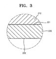
- FIG. 3 is an enlarged view of portion A of FIG. 2 ;
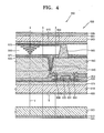
- FIG. 4 is a cross-sectional view of a liquid crystal display apparatus according to another embodiment of the present invention.
- FIG. 5 is an enlarged view of portion B of FIG. 4 ;
- FIG. 6 is a perspective view illustrating a first polarization layer of the liquid crystal display apparatus of FIG. 4 ;
- FIG. 7 is a graph illustrating a relationship between the wavelength of visible light and the reflectance of each of materials of the first polarization layer of the liquid crystal display apparatus of FIG. 4 ;
- FIG. 8 is a graph illustrating a relationship between the wavelength of visible light and the polarization extinction ratio of each of materials of the first polarization layer of the liquid crystal display apparatus of FIG. 1 ;
- FIG. 9 is a cross-sectional view of a liquid crystal display apparatus according to another embodiment of the present invention.
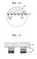
- FIG. 10 is an enlarged view of portion C of the liquid crystal display apparatus of FIG. 9 ;
- FIG. 11 is an enlarged view of grids of portion C of FIG. 10 ;
- FIG. 12 is a graph illustrating a relationship between the content of each of a first component and a second component and the thickness of each of the grids of FIG. 10 .
- FIG. 1 is a perspective view of a liquid crystal display apparatus 100 according to an embodiment of the present invention.
- FIG. 2 is a cross-sectional view taken along line II-II of FIG. 1 .
- FIG. 3 is an enlarged view of portion A of FIG. 2 .
- the liquid crystal display apparatus 100 includes a backlight unit 300, a liquid crystal layer 260, a first polarization layer 220, and a second polarization layer 290.
- the liquid crystal display apparatus 100 also can be described to include a liquid crystal display panel 200 and a backlight unit 300 supplying light to the liquid crystal display panel 200.
- a flexible printed circuit (FPC) board 205 for transmitting an image signal is attached to the liquid crystal display panel 200.
- the backlight unit 300 is disposed at the back of the liquid crystal display panel 200.
- the backlight unit 300 is supplied with power through a connection cable 305, and emits light through a front surface of the backlight unit 300.
- the light emitted by the backlight unit 300 is marked with arrows in FIGS. 1 and 2 .
- the light emitted by the backlight unit 300 is supplied to the liquid crystal display panel 200.
- a reflective layer 320 is disposed on a rear surface of the backlight unit 300 that is opposite to the front surface of the backlight unit 300 facing the liquid crystal layer 260.
- the reflective layer 320 reflects light emitted by the backlight unit 300 toward the liquid crystal display layer 260, thereby improving light efficiency.
- a quarter wavelength retardation layer 310 is disposed between the reflective layer 320 and the backlight unit 300.
- the liquid crystal display panel 200 includes the liquid crystal layer 260, and the first polarization layer 220 and the second polarization layer 290 disposed on each end of the liquid crystal layer 260, respectively. A detailed explanation of the liquid crystal display panel 200 will now be presented with reference to FIG. 2 .
- the liquid crystal display panel 200 includes a first substrate 210.
- the first substrate 210 is a transparent substrate.
- the first substrate 210 may be formed of a transparent glass material having SiO 2 as a main component, or formed of a transparent plastic material.
- the first polarization layer 220 is formed on a surface of the first substrate 210 facing the backlight unit 300.
- a detailed construction of the first polarization layer 220 is illustrated in FIG. 3 that is an enlarged view of the portion A of FIG. 2 .
- the first polarization layer 220 has an absorbent surface 221 and a reflective surface 222.
- the reflective surface 222 of the first polarization layer 220 faces the backlight unit 300, and the absorbent surface 221 of the first polarization layer 220, which is opposite to the surface of the first polarization layer 220 facing the backlight unit 300, faces the first substrate 210.
- the first polarization layer 220 may be formed by applying a reflective material to form the reflective surface 222, by applying an absorbent material to form the absorbent surface 221, and by patterning both the reflective material and the absorbent material.
- a reflective material to form the reflective surface 222
- an absorbent material to form the absorbent surface 221
- the first polarization layer 220 may be formed by forming the absorbent surface 221 and doping a reflective material on a surface of the absorbent surface 221 to from the reflective surface 222, or may be formed by using other methods.
- a buffer layer 211 is formed on a surface of the first substrate 210 opposite to the surface of the first substrate 210 on which the first polarization layer 220 is formed.
- the buffer layer 211 is used to maintain the smoothness of the first substrate 210 and prevent impurities from leaking.
- the buffer layer 211 may be formed of SiO 2 and/or SiNx.
- An active layer 231 may be formed on the buffer layer 211 in a predetermined pattern.
- a gate insulating layer 232 is formed on the active layer 231, and a gate electrode 233 is formed on the gate insulating layer 232 in a predetermined pattern.
- An inter-layer insulating layer 234 is formed on the gate electrode 233 to cover the gate electrode 233.
- the gate insulating layer 232 and the inter-layer insulating layer 234 are etched by dry etching or the like to form contact holes through which portions of the active layer 231 are exposed.
- a source electrode 235 and a drain electrode 236 are formed such that the source electrode 235 and the drain electrode 236 are electrically connected to the active layer 231 through the contact holes.
- a passivation layer 240 is formed to cover the source electrode 235 and the drain electrode 236, and a planarization layer 250 is formed on the passivation layer 240.
- the planarization layer 250 and the passivation layer 240 are etched to form a first electrode 255 in a predetermined pattern such that the first electrode 255 is electrically connected to the source electrode 235 or the drain electrode 236.
- a second substrate 280 is disposed to face the first substrate 210.
- the second substrate 280 is formed of a transparent material like the first substrate 210.
- the liquid crystal layer 260 is disposed between the first substrate 210 and the second substrate 280.
- a color filter layer 285 is formed on a bottom surface of the second substrate 280.
- a second electrode 275 is formed on a bottom surface of the color filter layer 285.
- a first alignment layer 271 and a second alignment layer 272 for aligning the liquid crystal layer 260 are formed on surfaces of the first electrode 255 and the second electrode 275 facing each other.
- the second polarization layer 290 is formed on a top surface of the second substrate 280.
- the second polarization layer 290 acts as an absorbent polarization layer.
- the second polarization layer 290 may include a phase shift layer.
- a protective film 295 is formed on the second polarization layer 290 in order to prevent damage from an external shock.
- a spacer 265 maintaining a space for the liquid crystal layer 260 is formed between the color filter layer 285 and the planarization layer 250.
- liquid crystal display panel 200 shown in FIG. 2 is a thin film transistor (TFT) liquid crystal display (LCD) panel
- TFT thin film transistor
- LCD liquid crystal display
- a potential difference is generated between the first electrode 255 and the second electrode 275 due to an external signal controlled by the gate electrode 233, the source electrode 235, and the drain electrode 236, the alignment of the liquid crystal layer 260 is determined by the potential difference, and visible light supplied by the backlight unit 300 is blocked or transmitted depending on the alignment of the liquid crystal layer 260.
- the backlight unit 300 is transmitted through the color filter layer 285, a color image is created.
- the first polarization layer 220 of the liquid crystal display apparatus 100 of FIG. 1 is disposed between the backlight unit 300 and the liquid crystal layer 260.
- the first polarization layer 220 has the absorbent surface 221 facing the liquid crystal layer 260. Accordingly, during an operation of the liquid crystal display apparatus 100, external light incident through the liquid crystal layer 260 reaches the first polarization layer 220.
- the absorbent surface 221 of the first polarization layer 220 prevents the external light from being reflected by the first polarization layer 220, thereby improving the contrast of the liquid crystal display apparatus 100. Also, the first polarization layer 220 has the reflective surface 222 facing the backlight unit 300.
- Light emitted by the backlight unit 300 tends to be randomly transmitted in different directions. That is, some of the light rays emitted by the backlight unit 300 travel toward the liquid crystal layer 260, and other of the light rays emitted by the backlight unit 300 travels away from the liquid crystal layer 260. As the amount of light travelling away from the liquid crystal layer 260 increases, light efficiency may decrease.
- a component of the light which vibrates along a reflection axis of the first polarization layer 220 that is perpendicular to the transmission axis of the first polarization layer 220, is reflected from the first polarization layer 220 by the reflective surface 222.
- the reflective surface 222 acts to selectively reflect light from the backlight unit 300 based on the polarization of the light from the backlight unit 300.
- the light reflected from the first polarization layer 220 is transformed into circularly polarized light rotating in one direction while passing through the quarter wavelength retardation layer 310.
- the circularly polarized light rotating in one direction is reflected by the reflective layer 320, and is transformed into circularly polarized light rotating in the opposite direction.
- the circularly polarized light rotating in the opposite direction is transformed into linearly polarized light that vibrates along the transmission axis of the first polarization layer 220 while passing through the quarter wavelength retardation layer 310, and thus transmits through the first polarization layer 220 to the liquid crystal layer 260.
- the first polarization layer 220 Since the light emitted by the backlight unit 300 is recycled and mostly directed to the liquid crystal layer 260, light efficiency can be improved. Also, since the first polarization layer 220 has the absorbent surface 221 and the reflective surface 222, the reflection of external light can be prevented and the efficiency of the backlight unit 300 can be improved. Since the first polarization layer 220 has the absorbent surface 221 and the reflective surface 222, an absorbent polarization layer and a reflective polarization layer do not need to be additionally formed.
- FIG. 4 is a cross-sectional view of a liquid crystal display apparatus 400 according to another embodiment of the present invention.
- FIG. 5 is an enlarged view of portion B of FIG. 4 .
- FIG. 6 is a perspective view illustrating a first polarization layer 620 of the liquid crystal display apparatus 400 of FIG. 4 .
- the same reference numeral denotes the same element.
- the liquid crystal display apparatus 400 includes a backlight unit 500, a liquid crystal layer 660, the first polarization layer 620, and a second polarization layer 690.
- the liquid crystal display apparatus 400 can be described to include a liquid crystal display panel 600 and the backlight unit 500.
- a reflective layer 520 is disposed on a surface of the backlight unit 500 opposite to a surface of the backlight unit 500 facing the liquid crystal layer 260.
- a quarter wavelength retardation layer 510 is disposed between the reflective layer 520 and the backlight unit 500.
- the liquid crystal display panel 600 includes the liquid crystal layer 660, and the first polarization layer 620 and the second polarization layer 690 disposed on each end of the liquid crystal layer 660, respectively.
- the liquid crystal display panel 600 includes a first substrate 610.
- the first polarization layer 620 is formed on a surface of the first substrate 610 facing the backlight unit 500.
- FIG. 5 A detailed construction of the first polarization layer 620 is illustrated in FIG. 5 that is an enlarged view of portion B of FIG. 4 .
- the first polarization layer 620 includes a plurality of grids 621 and a plurality of absorbing members 622.
- Each of the grids 621 includes a metal that reflects light.
- the grids 621 are arranged to face the backlight unit 500, and the absorbing members 622 are arranged to face the liquid crystal layer 660. In general, the absorbing members are arranged closer than the grids to the liquid crystal layer. Referring to FIG. 5 , the absorbing members 622 are disposed between the first substrate 610 and the grids 621.
- the grids 621 form a first pattern of grid members and the absorbing members 622 form a second pattern of grid members, which in this embodiment are joined together as shown in FIG. 5 and 6 .
- the grids 621 are formed by arranging conductive lines in parallel to polarize specific wavelengths of electromagnetic waves.
- Each of the grids 621 may be formed of a conductor such as aluminum, silver, or chrome.
- the grids 621 are arranged at intervals.
- a pitch P1 which is an interval between two grids 621, is an important factor determining the performance of the grids 621. If the pitch P1 of the grids 621 is greater than the wavelength of incident light, the grids 621 act as a diffraction grating rather than as a polarizer. On the contrary, if the pitch P1 of the grids 621 is smaller than the wavelength of incident light, the grids 621 mainly act as a polarizer.
- the first polarization layer 620 includes the absorbing members 622.
- the absorbing members 622 are formed between the grids 621 and the first substrate 610.
- the thickness T2 of each of the absorbing members 622 may be different from the thickness T1 of the grids 621, and a pitch P2 of the absorbing members 622, which is an interval between two absorbing members 622, may be the same as the pitch P1 of the grids 621.
- the absorbing members 622 may be formed of a material having a low reflectance.
- Each of the absorbing members 622 may be formed of any of various materials including cadmium selenide (CdSe), cadmium telluride (CdTe), and ruthenium.
- Each of the absorbing members 622 may include a dielectric material, and a mixture of the dielectric material and the metal.
- FIG. 7 is a graph illustrating the reflectance of each of materials as a function of a wavelength of visible light.
- FIG. 8 is a graph illustrating the polarization extinction ratio of each of materials as a function of a wavelength of visible light.
- the first polarization layer 620 was constructed as described with reference to FIGS. 7 and 8 , and the first polarization layer 620 was examined.
- the grids 621 had a pitch P1 of 100 nanometers, a width W1 of 50 nanometers, and a thickness T1 of 100 nanometers.
- the absorbing members 622 had a pitch P2 of 100 nanometers, a width W2 of 50 nanometers, and a thickness T2 of 100 nanometers.
- the horizontal axis represents a wavelength of visible light and the vertical axis represents the reflectance of each material.
- aluminum has a reflectance of higher than 50 % in wavelengths of blue, green, and red light.
- CdSe, CdTe, and ruthenium which are used to form the absorbing members 622 included in the first polarization layer 620 of the liquid crystal display apparatus 400 of FIG. 4 , have a reflectance lower than 30 %, which is much lower than that of aluminum.
- Table 1 shows data of FIG. 7 .
- each of CdSe, CdTe, and Ruthenium has a reflectance of 30 % or less in the wavelengths of blue, green, and red light.
- each of CdSe, CdTe, and Ruthenium is also superior to aluminum in terms of a polarization extinction ratio.
- the horizontal axis represents a wavelength of visible light
- the vertical axis represents the polarization extinction ratio of each material.
- a polarization extinction ratio refers to a ratio of the optical power of an incident S wave to the optical power of a transmitted S wave when S-polarized light is incident. As a polarization extinction ratio increases, polarization performance increases. Table 2 shows data of FIG. 8 .
- each of CdSe and CdTe has a polarization extinction ratio about twice greater than that of aluminum, and ruthenium has a polarization extinction ratio about 1000 times greater than that of aluminum.
- each of the absorbing members 622 may include a dielectric material.
- Each of the absorbing members 622 may include any of various dielectric materials including an organic material or an inorganic material.
- Each of the absorbing members 622 may be formed of an inorganic material such as SiOx (x ⁇ 1), SiNx (x ⁇ 1), MgF 2 , CaF 2 , Al 2 O 3 , SnO 2 indium tin oxide (ITO), indium zinc oxide (IZO), ZnO, In 2 O 3 , Cr 2 O 3 , Ag 2 O, TiO 2 , Ta 2 O 5 , HfO 2 , or a nitride.
- Each of the absorbing members 622 may be formed of an organic material such as polyethylene (PE), polypropylene (PP), polystyrene(PS), polyethylene terephthalate (PET or PETE), polyamide(PA), polyester, polyvinyl chloride (PVC), polycarbonate (PC), acrylonitrile butadiene styrene (ABS), polyvinylidene chloride (PVDC), polytetrafluoroethylene (PTFE), polymethyl methacrylate (PMMA), polylactic acid (PLA), or polyurethane (PU).
- Each of the absorbing members 622 may be formed of a low molecular organic material such as copper phthalocyanine (CuPc), N,N'-Di(naphthalene-1-yl)-N,N'-diphenyl-benzidine (NPB), or tris-8-hydroxyquinoline aluminum) (Alq3).
- CuPc copper phthalocyanine
- NPB N,N'-Di(naphthalene-1-yl)-N,N'-diphenyl-benzidine
- Alq3 tris-8-hydroxyquinoline aluminum
- Each of the absorbing members 622 may include a metal, and a mixture of the metal and the dielectric material. That is, low reflective members having a low reflectance and a high absorption coefficient may be formed by co-depositing a metal and a dielectric material to form a mixture.
- the metal may include Fe, Co, V, Ti, Al, Ag, Si, Cr, Mo, Ge, Y, Zn, Zr, W, Ta, Cu, and Pt.
- Examples of the dielectric material that is mixed with the metal may include an organic material, an inorganic material, or a compound of the organic material and the inorganic material.
- Examples of the inorganic material that is mixed with the metal may include SiOx (x ⁇ 1), SiNx (x ⁇ 1), MgF 2 , CaF 2 , Al 2 O 3 , SnO 2 ITO, IZO, ZnO, In 2 O 3 , Cr 2 O 3 , Ag 2 O, TiO 2 , Ta 2 O 5 , HfO 2 , and a nitride.
- Examples of the organic material that is mixed with the metal may include a high molecular material such as PE, PP, PS, PET or PETE, PA, polyester, PVC, PC, ABS, PVDC, PTFE, PMMA, PLA, or PU, or a low molecular organic material such as CuPc, NPB, or Alq3.
- Each of the absorbing members 622 may be formed by mixing a compound of the organic materials and the inorganic materials with the metal.
- the absorbing members 622 are formed on the grids 621 and cover top surfaces of the grids 621 as shown in FIG. 5 . That is, when external light is incident on the first polarization layer 620, the absorbing members 622 prevent the external light from being reflected from the grids 621 formed of a metal. To this end, the width W2 of the absorbing members 622 may be the same as the width W 1 of the grids 621.
- the first polarization layer 620 is patterned such that the grids 621 and the absorbing members 622 are linearly arranged at predetermined intervals as shown in FIG. 6 .
- the first polarization layer 620 of FIG. 6 can be easily formed by coating the first substrate 610 with a material to form the absorbing members 622, by coating the absorbing member-coated first substrate with a material to from the grids 621, and by performing a patterning process using a mask.
- the first polarization layer 620 may be formed by forming a material on the backlight unit 500 to form the grids 621, by forming a material to form the absorbing members 622, and by performing a patterning process.
- a buffer layer 611 is formed on a surface of the first substrate 610 opposite to the surface of the first substrate 610 on which the first polarization layer 620 is formed.
- An active layer 631 is formed in a predetermined pattern on the buffer layer 611.
- a gate insulating layer 632 is formed on the active layer 631.
- a gate electrode 633 is formed in a predetermined pattern on the gate insulating layer 632.
- An inter-layer insulating layer 634 is formed on the gate electrode 633. Next, contact holes are formed, and a source electrode 635 and a drain electrode 636 are formed such that the source electrode 635 and the drain electrode 636 are electrically connected to the active layer 631 through the contact holes.
- a passivation layer 640 is formed to cover the source electrode 635 and the drain electrode 636.
- a planarization layer 650 is formed on the passivation layer 640.
- a first electrode 655 is formed in a predetermined pattern such that the first electrode 655 is electrically connected to the source electrode 635 or the drain electrode 636.
- a second substrate 680 is disposed to face the first substrate 610.
- the liquid crystal layer 660 is disposed between the first substrate 610 and the second substrate 680.
- a color filter layer 685 is formed on a bottom surface of the second substrate 680.
- a second electrode 675 is formed on a bottom surface of the color filter layer 685.
- a first alignment layer 671 and a second alignment layer 672 aligning the liquid crystal layer 660 are formed on surfaces of the first electrode 655 and the second electrode 675 facing each other.
- the second polarization layer 690 is formed on a top surface of the second substrate 680.
- the second polarization layer 690 acts as an absorbent polarization layer.
- the second polarization layer 690 may include a phase shift layer.
- a protective film 695 is formed on the second polarization layer 690.
- a spacer 665 maintaining a space for the liquid crystal layer 660 is formed between the color filter layer 685 and the planarization layer 650.
- the first polarization layer 620 of the liquid crystal display apparatus 400 of FIG. 4 is disposed between the backlight unit 500 and the liquid crystal layer 660.
- the first polarization layer 620 includes the absorbing members 622 facing the liquid crystal layer 260.
- the liquid crystal display apparatus 400 Accordingly, during the operation of the liquid crystal display apparatus 400, external light incident through the liquid crystal layer 660 reaches the first polarization layer 620.
- the absorbing members 622 of the first polarization layer 620 prevent the external light from being reflected from the first polarization layer 620, thereby improving the contrast of the liquid crystal display apparatus 400.
- the first polarization layer 620 has the grids 621, each of which includes a metal and faces the backlight unit 500. Light emitted by the backlight unit 500 is reflected from the grids 621, and then is reflected again by the reflective layer 520, thereby improving light efficiency and brightness.
- the grid members 621 act to selectively reflect light from the backlight unit 500 based on the polarization of the light from the backlight unit 500.
- the light reflected from the first polarization layer 620 is transformed into circularly polarized light rotating in one direction while passing through the quarter wavelength retardation layer 510.
- the circularly polarized light rotating in one direction is reflected by the reflective layer 520, and is transformed into circularly polarized light rotating in the opposite direction.
- the circularly rotating light rotating in the opposite direction is transformed into linearly polarized light that vibrates along the transmission axis of the first polarization layer 620, and thus transmits through the first polarization layer 620 to the liquid crystal layer 660.
- FIG. 9 is a cross-sectional view of a liquid crystal display apparatus 700 according to another embodiment of the present invention.
- FIG. 10 is an enlarged view of portion C of the liquid crystal display apparatus 700 of FIG. 9 .
- FIG. 11 is an enlarged view of a plurality of grids 821 of portion C of FIG. 10 .
- FIG. 12 is a graph illustrating the content of each of a first component and a second component as a function of the thickness of each of the grids 821 of FIG. 10 .
- the grids 821 form a pattern of grid members, and it can be considered that the first component and the second component of grids 821 form first and second patterns of grid members.
- the liquid crystal display apparatus 700 includes a backlight unit 900, a liquid crystal layer 860, a first polarization layer 820, and a second polarization layer 890.
- the liquid crystal display apparatus 700 can be described to include a liquid crystal display panel 800 and the backlight unit 900.
- a reflective layer 920 is disposed on a surface of the backlight unit 900 opposite to a surface of the backlight unit 900 facing the liquid crystal layer 860.
- a quarter wavelength retardation layer 910 is disposed between the reflective layer 920 and the backlight unit 900.
- the liquid crystal display panel 800 includes the liquid crystal layer 860, and the first polarization layer 820 and the second polarization layer 890 disposed on both ends of the liquid crystal layer 860.
- the liquid crystal display panel 800 includes a first substrate 810.
- the first polarization layer 820 is formed on a surface of the first substrate 810 facing the backlight unit 900.
- a detailed construction of the first polarization layer 820 is illustrated in FIG. 10 that is an enlarged view of portion C of FIG. 9 .
- the first polarization layer 820 includes the plurality of grids 821.
- the grids 821 may be patterned into stripes that are arranged at predetermined intervals.
- a pitch P3 of the grids 821 is an important factor in determining the performance of the grids 821. If the pitch P3 of the grids 821 is greater than the wavelength of incident light, the grids 821 act as a diffraction grating rather than as a polarizer. On the contrary, if the pitch P3 of the grids 821 is smaller than the wavelength of incident light, the grids 821 mainly act as a polarizer.
- the grids 621 may have a width W3 of 100 to 500 nanometers and a thickness T3 of 300 to 500 nanometers.
- Each of the grids 821 includes a first component 821a and a second component 821b.
- a detailed construction of each of the grids 821 is illustrated in FIG. 11 that is an enlarged view of the grids 821 portion of FIG. 10 .
- the first component 821a includes a dielectric material
- the second component 821b includes a metal.
- the content of the first component 821a increases while proceeding toward the liquid crystal layer 860.
- the content of the second component 821b increases while proceeding toward the backlight unit 900.
- the first component 821a may be formed of an insulating transparent material such as SiOx (x ⁇ 1), SiNx (x ⁇ 1), MgF 2 , CaF 2 , Al 2 O 3 , or SnO 2
- the first component 821a may be formed of a conductive transparent material such as ITO, IZO, ZnO, or In 2 O 3 .
- the second component 821b includes a metal.
- the second component 821b may be formed of Fe, Co, V, Ti, Al, Ag, Si, Cr, Mo, Ge, Y, Zn, Zr, W, Ta, Cu, or Pt.
- Each of the grids 821 has a concentration gradient such that the first component 821a is more concentrated near the liquid crystal layer 860 and the second component 821b is more concentrated near the backlight unit 900.
- the content of the first component 821a increases as proceeding toward the first substrate 810, and the content of the second component 821b increases as proceeding away from the first substrate 810. That is, the first component 821 is more concentrated at a location near to the first substrate 810, and the second component 821b is more concentrated at a location far from the first substrate 810.
- External light is incident on the first polarization layer 820 through the liquid crystal layer 860.
- the content of the first component 821a, which is formed of a dielectric material, of each of the grids 821 of the first polarization layer 820 increases as proceeding toward the external light.
- a ratio of a transparent material to an opaque metal in each of the grids 821 increases gradually while proceeding toward the first substrate 810, specifically, toward the liquid crystal layer 860, thereby preventing an interfacial reflection that may be caused by a difference of refractive indices. Accordingly, when external light is incident on the grids 821, the grids 821 absorbs the external light, thereby preventing the reflection of the external light.
- Co-deposition or the like may be used to form the grids 821 having a concentration gradient.
- deposition rates of the first component 821a and the content of the second component 821b can be adjusted with respect to time so that the content of the first component 821a is inversely proportional to the content of the second component 821b.
- a buffer layer 811 is formed on a surface of the first substrate 810 opposite to the surface of the first substrate 810 on which the first polarization layer 820 is formed.
- An active layer 831 is formed in a predetermined pattern on the buffer layer 811.
- a gate insulating layer 832 is formed on the active layer 831.
- a gate electrode 833 is formed in a predetermined pattern on the gate insulating layer 832.
- An inter-layer insulating layer 834 is formed on the gate electrode 833.
- contact holes are formed, and a source electrode 835 and a drain electrode 836 are formed such that the source electrode 835 and the drain electrode 836 are electrically connected to the active layer 831 through the contact holes.
- a passivation layer 840 is formed to cover the source electrode 835 and the drain electrode 836.
- a planarization layer 850 is formed on the passivation layer 840.
- a first electrode 855 is formed in a predetermined pattern such that the first electrode 855 is electrically connected to the source electrode 835 or the drain electrode 836.
- a second substrate 880 is disposed to face the first substrate 810.
- the liquid crystal layer 860 is disposed between the first substrate 810 and the second substrate 880.
- a color filter layer 885 is formed on a bottom surface of the second substrate 880.
- a second electrode 875 is formed on a bottom surface of the color filter layer 885.
- a first alignment layer 871 and a second alignment layer 872 aligning the liquid crystal layer 860 are formed on surfaces of the first electrode 855 and the second electrode 875 facing each other.
- the second polarization layer 890 is formed on a top surface of the second substrate 880.
- the second polarization layer 890 acts as an absorbent polarization layer 890.
- the second polarization layer 890 may include a phase shift layer.
- a protective film 895 is formed on the second polarization layer 890.
- a spacer 865 maintaining a space for the liquid crystal layer 860 is formed between the color filter layer 885 and the planarization layer 850.
- the first polarization layer 820 of the liquid crystal display apparatus 700 of FIG. 9 is disposed between the backlight unit 900 and the liquid crystal layer 860.
- the first polarization layer 820 includes the plurality of grids 821.
- Each of the grids 821 includes the first component 821a and the second component 821b.
- a ratio of an opaque metal to a transparent material increases gradually while proceeding toward the backlight unit 900. Accordingly, light emitted by the backlight unit 900 is reflected by the grids 821, and then is reflected again by the reflective layer 920, thereby improving light efficiency and brightness.
- Light emitted by the backlight unit 900 tends to randomly travel in different directions. That is, some of the light rays emitted by the backlight unit 900 travel toward the liquid crystal layer 860 and the other of the light rays emitted by the backlight unit 900 travels away from the liquid crystal layer 860. As the amount of light rays traveling away from the liquid crystal layer 860 increases, light efficiency may decrease. However, in the liquid crystal display apparatus 700 of FIG. 9 , even though some of the light rays emitted by the backlight unit 900 travels away from the liquid crystal layer 860, the light is reflected from the reflective layer 920 toward the liquid crystal layer 860, thereby preventing a reduction in light efficiency.
- the backlight unit 900 when light emitted by the backlight unit 900 reaches the first polarization layer 820 while travelling toward the liquid crystal layer 860, a component of the light which vibrates along a transmission axis of the first polarization layer 820, among other components of the light vibrating along other axes, transmits through the first polarization layer 820 to the liquid crystal layer 860.
- a component of the light which vibrates along a reflection axis of the first polarization layer 820 that is perpendicular to the transmission axis of the first polarization layer 820, is reflected by the second component 821b of the grids 621 on the first polarization layer 820.
- the second component 821b of the grids 621 act to selectively reflect light from the backlight unit backlight unit 900 based on the polarization of the light from the backlight unit 900.
- the light reflected by the polarization layer 820 is transformed into circularly polarized light rotating in one direction while passing through the quarter wavelength retardation layer 910.
- the circularly polarized light rotating in one direction is reflected by the reflective layer 920, and is transformed into circularly polarized light rotating in the opposite direction.
- the circularly polarized light rotating in the opposite direction is transformed into linearly polarized light that vibrates along the transmission axis of the first polarization layer 820 while passing through the quarter wavelength retardation layer 910, and thus transmits through the first polarization layer 820 to the liquid crystal layer 860.
- the backlight unit 900 Since the light emitted by the backlight unit 900 is recycled and mostly directed to the liquid crystal layer 860, light efficiency can be improved.
- each of the grids 821 of the first polarization layer 820 has a concentration gradient such that the content of the first component 821a a acing as an absorbing member increases while proceeding toward the liquid crystal layer 860 and the content of the second component 821b acting as a reflecting member increases while proceeding toward the backlight unit 900, the reflection of external light can be prevented and the efficiency of the backlight unit 900 can be improved.
- the first polarization layer 820 includes the grids 821, each of which includes the first component 821a acting as the absorbing member and the second component 821b acting as the reflecting member, additionally forming an absorbent polarization layer and a reflective polarization layer may not be necessary.
- the liquid crystal display apparatus can prevent the reflection of external light and can improve contrast and visibility by disposing a polarization layer having a reflective surface and an absorbent surface between a liquid crystal layer and a backlight unit, and can improve brightness by improving the efficiency of the backlight unit.
Landscapes
- Physics & Mathematics (AREA)
- Nonlinear Science (AREA)
- General Physics & Mathematics (AREA)
- Optics & Photonics (AREA)
- Mathematical Physics (AREA)
- Chemical & Material Sciences (AREA)
- Crystallography & Structural Chemistry (AREA)
- Liquid Crystal (AREA)
- Polarising Elements (AREA)
- Devices For Indicating Variable Information By Combining Individual Elements (AREA)
Applications Claiming Priority (1)
| Application Number | Priority Date | Filing Date | Title |
|---|---|---|---|
| KR20080040803A KR100927587B1 (ko) | 2008-04-30 | 2008-04-30 | 액정 표시 장치 |
Publications (3)
| Publication Number | Publication Date |
|---|---|
| EP2116891A2 true EP2116891A2 (de) | 2009-11-11 |
| EP2116891A3 EP2116891A3 (de) | 2009-12-02 |
| EP2116891B1 EP2116891B1 (de) | 2014-01-01 |
Family
ID=40910038
Family Applications (1)
| Application Number | Title | Priority Date | Filing Date |
|---|---|---|---|
| EP20090251229 Not-in-force EP2116891B1 (de) | 2008-04-30 | 2009-04-30 | Flüssigkristallanzeigevorrichtung |
Country Status (5)
| Country | Link |
|---|---|
| US (1) | US8384854B2 (de) |
| EP (1) | EP2116891B1 (de) |
| JP (2) | JP2009271526A (de) |
| KR (1) | KR100927587B1 (de) |
| CN (2) | CN101571643A (de) |
Families Citing this family (8)
| Publication number | Priority date | Publication date | Assignee | Title |
|---|---|---|---|---|
| KR102055683B1 (ko) * | 2013-03-29 | 2019-12-16 | 삼성디스플레이 주식회사 | 유기 발광 표시 장치 |
| KR20150012526A (ko) | 2013-07-25 | 2015-02-04 | 삼성전자주식회사 | 디스플레이 패널 및 이를 가지는 디스플레이장치 |
| KR20160001174A (ko) | 2014-06-26 | 2016-01-06 | 삼성전자주식회사 | 디스플레이 패널의 선형격자의 제조방법 |
| CN106526952A (zh) * | 2016-12-26 | 2017-03-22 | 南京中电熊猫液晶显示科技有限公司 | 彩膜基板及其制造方法、以及液晶显示器 |
| CN109581568B (zh) * | 2017-09-28 | 2022-05-24 | 迪睿合株式会社 | 偏振光板及具备该偏振光板的光学设备 |
| JP6678630B2 (ja) * | 2017-09-28 | 2020-04-08 | デクセリアルズ株式会社 | 偏光板及びこれを備える光学機器 |
| CN108181677A (zh) * | 2017-12-28 | 2018-06-19 | 深圳市华星光电技术有限公司 | 偏光片、液晶面板及液晶显示器 |
| JP2018189980A (ja) * | 2018-07-19 | 2018-11-29 | デクセリアルズ株式会社 | 偏光板 |
Family Cites Families (22)
| Publication number | Priority date | Publication date | Assignee | Title |
|---|---|---|---|---|
| JP2902456B2 (ja) * | 1990-08-09 | 1999-06-07 | 株式会社豊田中央研究所 | 無機偏光薄膜 |
| US5445898A (en) * | 1992-12-16 | 1995-08-29 | Westinghouse Norden Systems | Sunlight viewable thin film electroluminescent display |
| KR100582861B1 (ko) | 1996-09-17 | 2006-05-25 | 세이코 엡슨 가부시키가이샤 | 표시 장치 및 그 표시 장치를 사용한 전자 기기 |
| JP3648870B2 (ja) * | 1996-09-24 | 2005-05-18 | セイコーエプソン株式会社 | 液晶表示装置 |
| US6398364B1 (en) * | 1999-10-06 | 2002-06-04 | Optical Coating Laboratory, Inc. | Off-axis image projection display system |
| CN1327545A (zh) * | 1999-10-29 | 2001-12-19 | 松下电器产业株式会社 | 液晶面板和液晶显示装置 |
| EP1111438A3 (de) * | 1999-12-23 | 2003-03-19 | Samsung SDI Co., Ltd. | Schwarzmatrix und deren Herstellungsverfahren |
| JP3598987B2 (ja) | 2001-03-28 | 2004-12-08 | セイコーエプソン株式会社 | 液晶表示装置および電子機器 |
| US6816216B2 (en) * | 2001-04-12 | 2004-11-09 | Omron Corporation | Optical component and reflective plate, and device using the same optical component |
| TW525020B (en) * | 2001-07-27 | 2003-03-21 | Chi Mei Optoelectronics Corp | Liquid crystal display |
| JP4425059B2 (ja) * | 2003-06-25 | 2010-03-03 | シャープ株式会社 | 偏光光学素子、およびそれを用いた表示装置 |
| US7466484B2 (en) * | 2004-09-23 | 2008-12-16 | Rohm And Haas Denmark Finance A/S | Wire grid polarizers and optical elements containing them |
| US7619816B2 (en) * | 2004-12-15 | 2009-11-17 | Api Nanofabrication And Research Corp. | Structures for polarization and beam control |
| JP2007003870A (ja) * | 2005-06-24 | 2007-01-11 | Seiko Epson Corp | 光学素子の製造方法、光学素子、投射型表示装置 |
| WO2007011047A1 (ja) * | 2005-07-22 | 2007-01-25 | Zeon Corporation | グリッド偏光子及びその製法 |
| KR100718136B1 (ko) * | 2005-08-30 | 2007-05-14 | 삼성전자주식회사 | 와이어 그리드 편광자를 이용한 백라이트 유닛 및 이를채용한 액정표시장치 |
| US20070242352A1 (en) * | 2006-04-13 | 2007-10-18 | Macmaster Steven William | Wire-grid polarizers, methods of fabrication thereof and their use in transmissive displays |
| KR20070117816A (ko) * | 2006-06-09 | 2007-12-13 | 삼성전자주식회사 | 편광판, 이의 제조방법 및 이를 갖는 표시패널 |
| JP4762804B2 (ja) * | 2006-06-28 | 2011-08-31 | チェイル インダストリーズ インコーポレイテッド | 偏光分離素子およびその製造方法 |
| KR100838066B1 (ko) | 2006-07-14 | 2008-06-16 | 삼성에스디아이 주식회사 | 유기 발광 장치 |
| JP4778873B2 (ja) * | 2006-10-20 | 2011-09-21 | 株式会社 日立ディスプレイズ | 液晶表示装置 |
| US7772768B2 (en) * | 2007-03-02 | 2010-08-10 | Samsung Mobile Display Co., Ltd. | Polarizer and flat panel display apparatus including the same |
-
2008
- 2008-04-30 KR KR20080040803A patent/KR100927587B1/ko not_active Expired - Fee Related
-
2009
- 2009-04-23 JP JP2009105473A patent/JP2009271526A/ja active Pending
- 2009-04-24 US US12/385,972 patent/US8384854B2/en active Active
- 2009-04-30 CN CNA2009101381137A patent/CN101571643A/zh active Pending
- 2009-04-30 EP EP20090251229 patent/EP2116891B1/de not_active Not-in-force
- 2009-04-30 CN CN201511021046.2A patent/CN105445997B/zh not_active Expired - Fee Related
-
2011
- 2011-10-12 JP JP2011224575A patent/JP5571641B2/ja not_active Expired - Fee Related
Non-Patent Citations (1)
| Title |
|---|
| None |
Also Published As
| Publication number | Publication date |
|---|---|
| US8384854B2 (en) | 2013-02-26 |
| KR20090114922A (ko) | 2009-11-04 |
| CN105445997B (zh) | 2019-12-13 |
| JP2012027492A (ja) | 2012-02-09 |
| KR100927587B1 (ko) | 2009-11-23 |
| JP2009271526A (ja) | 2009-11-19 |
| EP2116891B1 (de) | 2014-01-01 |
| US20090273728A1 (en) | 2009-11-05 |
| JP5571641B2 (ja) | 2014-08-13 |
| EP2116891A3 (de) | 2009-12-02 |
| CN105445997A (zh) | 2016-03-30 |
| CN101571643A (zh) | 2009-11-04 |
Similar Documents
| Publication | Publication Date | Title |
|---|---|---|
| EP2116891B1 (de) | Flüssigkristallanzeigevorrichtung | |
| US8068266B2 (en) | Display substrate, method of manufacturing the same and electrowetting display panel having the display substrate | |
| US9568767B2 (en) | Display apparatus | |
| KR100800932B1 (ko) | 표시 장치 | |
| US10317694B2 (en) | Color filter-integrated polarizer and method of manufacturing the same | |
| US20190025641A1 (en) | Color filter substrate, display panel and display apparatus containing the color filter substrate | |
| KR20170056558A (ko) | 광 제어 장치, 광 제어 장치의 제조 방법 및 광 제어 장치를 포함하는 표시 장치 | |
| KR20170052596A (ko) | 광 제어 장치, 광 제어 장치의 제조 방법 및 광 제어 장치를 포함하는 표시 장치 | |
| KR20130013534A (ko) | 횡전계형 액정표시장치용 어레이 기판 | |
| US20160033701A1 (en) | Wire grid polarizer and method of fabricating the same | |
| US20060238679A1 (en) | Display device | |
| JP2007041536A (ja) | 表示装置及び液晶表示装置 | |
| JP2006323302A (ja) | 表示装置 | |
| JP2006323303A (ja) | 表示装置 | |
| KR20060086174A (ko) | 일체형 액정 표시 장치 | |
| US20060274239A1 (en) | Liquid crystal display and method of manufacturing of a TFT array panel of the same | |
| US20050179841A1 (en) | Transmissive and reflective mode fringe field switching liquid crystal display | |
| WO2007046209A1 (ja) | 液晶表示装置 | |
| KR102602160B1 (ko) | 백라이트 유닛, 백라이트 유닛을 포함하는 표시 장치 및 표시 장치를 제조하는 방법 | |
| KR102081979B1 (ko) | 표시 장치 | |
| US20210181575A1 (en) | Reflective display panel and manufacturing thereof, and display device | |
| JP4826997B2 (ja) | 表示装置 | |
| KR20060046964A (ko) | 표시 패널 및 이를 구비한 표시 장치 | |
| KR20110031010A (ko) | 반사투과형 액정표시소자 | |
| KR100936956B1 (ko) | 반투과형 액정 표시장치 |
Legal Events
| Date | Code | Title | Description |
|---|---|---|---|
| PUAI | Public reference made under article 153(3) epc to a published international application that has entered the european phase |
Free format text: ORIGINAL CODE: 0009012 |
|
| PUAL | Search report despatched |
Free format text: ORIGINAL CODE: 0009013 |
|
| 17P | Request for examination filed |
Effective date: 20090527 |
|
| AK | Designated contracting states |
Kind code of ref document: A2 Designated state(s): AT BE BG CH CY CZ DE DK EE ES FI FR GB GR HR HU IE IS IT LI LT LU LV MC MK MT NL NO PL PT RO SE SI SK TR |
|
| AK | Designated contracting states |
Kind code of ref document: A3 Designated state(s): AT BE BG CH CY CZ DE DK EE ES FI FR GB GR HR HU IE IS IT LI LT LU LV MC MK MT NL NO PL PT RO SE SI SK TR |
|
| RIC1 | Information provided on ipc code assigned before grant |
Ipc: G02F 1/1335 20060101AFI20110126BHEP Ipc: G02B 5/30 20060101ALI20110126BHEP |
|
| 17Q | First examination report despatched |
Effective date: 20110224 |
|
| RAP1 | Party data changed (applicant data changed or rights of an application transferred) |
Owner name: SAMSUNG DISPLAY CO., LTD. |
|
| GRAP | Despatch of communication of intention to grant a patent |
Free format text: ORIGINAL CODE: EPIDOSNIGR1 |
|
| INTG | Intention to grant announced |
Effective date: 20130704 |
|
| RIN1 | Information on inventor provided before grant (corrected) |
Inventor name: HWANG, KYU-HWAN Inventor name: SONG, YOUNG-WOO Inventor name: OH,JONG-SEOK Inventor name: LEE, JONG-HYUK Inventor name: LEE,JOON-GU Inventor name: HA, JAE-HEUNG Inventor name: PARK, CHUL-WOO |
|
| GRAS | Grant fee paid |
Free format text: ORIGINAL CODE: EPIDOSNIGR3 |
|
| GRAA | (expected) grant |
Free format text: ORIGINAL CODE: 0009210 |
|
| RIN1 | Information on inventor provided before grant (corrected) |
Inventor name: HA, JAE-HEUNG Inventor name: LEE,JOON-GU Inventor name: HWANG, KYU-HWAN Inventor name: SONG, YOUNG-WOO Inventor name: LEE, JONG-HYUK Inventor name: PARK, CHUL-WOO Inventor name: OH,JONG-SEOK |
|
| AK | Designated contracting states |
Kind code of ref document: B1 Designated state(s): AT BE BG CH CY CZ DE DK EE ES FI FR GB GR HR HU IE IS IT LI LT LU LV MC MK MT NL NO PL PT RO SE SI SK TR |
|
| REG | Reference to a national code |
Ref country code: GB Ref legal event code: FG4D |
|
| REG | Reference to a national code |
Ref country code: CH Ref legal event code: EP |
|
| REG | Reference to a national code |
Ref country code: IE Ref legal event code: FG4D |
|
| REG | Reference to a national code |
Ref country code: AT Ref legal event code: REF Ref document number: 647837 Country of ref document: AT Kind code of ref document: T Effective date: 20140215 |
|
| REG | Reference to a national code |
Ref country code: DE Ref legal event code: R096 Ref document number: 602009021116 Country of ref document: DE Effective date: 20140220 |
|
| REG | Reference to a national code |
Ref country code: NL Ref legal event code: VDEP Effective date: 20140101 |
|
| REG | Reference to a national code |
Ref country code: AT Ref legal event code: MK05 Ref document number: 647837 Country of ref document: AT Kind code of ref document: T Effective date: 20140101 |
|
| REG | Reference to a national code |
Ref country code: LT Ref legal event code: MG4D |
|
| PG25 | Lapsed in a contracting state [announced via postgrant information from national office to epo] |
Ref country code: IS Free format text: LAPSE BECAUSE OF FAILURE TO SUBMIT A TRANSLATION OF THE DESCRIPTION OR TO PAY THE FEE WITHIN THE PRESCRIBED TIME-LIMIT Effective date: 20140501 Ref country code: LT Free format text: LAPSE BECAUSE OF FAILURE TO SUBMIT A TRANSLATION OF THE DESCRIPTION OR TO PAY THE FEE WITHIN THE PRESCRIBED TIME-LIMIT Effective date: 20140101 |
|
| PG25 | Lapsed in a contracting state [announced via postgrant information from national office to epo] |
Ref country code: FI Free format text: LAPSE BECAUSE OF FAILURE TO SUBMIT A TRANSLATION OF THE DESCRIPTION OR TO PAY THE FEE WITHIN THE PRESCRIBED TIME-LIMIT Effective date: 20140101 Ref country code: AT Free format text: LAPSE BECAUSE OF FAILURE TO SUBMIT A TRANSLATION OF THE DESCRIPTION OR TO PAY THE FEE WITHIN THE PRESCRIBED TIME-LIMIT Effective date: 20140101 Ref country code: CY Free format text: LAPSE BECAUSE OF FAILURE TO SUBMIT A TRANSLATION OF THE DESCRIPTION OR TO PAY THE FEE WITHIN THE PRESCRIBED TIME-LIMIT Effective date: 20140101 Ref country code: SE Free format text: LAPSE BECAUSE OF FAILURE TO SUBMIT A TRANSLATION OF THE DESCRIPTION OR TO PAY THE FEE WITHIN THE PRESCRIBED TIME-LIMIT Effective date: 20140101 Ref country code: PT Free format text: LAPSE BECAUSE OF FAILURE TO SUBMIT A TRANSLATION OF THE DESCRIPTION OR TO PAY THE FEE WITHIN THE PRESCRIBED TIME-LIMIT Effective date: 20140502 Ref country code: ES Free format text: LAPSE BECAUSE OF FAILURE TO SUBMIT A TRANSLATION OF THE DESCRIPTION OR TO PAY THE FEE WITHIN THE PRESCRIBED TIME-LIMIT Effective date: 20140101 Ref country code: NL Free format text: LAPSE BECAUSE OF FAILURE TO SUBMIT A TRANSLATION OF THE DESCRIPTION OR TO PAY THE FEE WITHIN THE PRESCRIBED TIME-LIMIT Effective date: 20140101 |
|
| PG25 | Lapsed in a contracting state [announced via postgrant information from national office to epo] |
Ref country code: LV Free format text: LAPSE BECAUSE OF FAILURE TO SUBMIT A TRANSLATION OF THE DESCRIPTION OR TO PAY THE FEE WITHIN THE PRESCRIBED TIME-LIMIT Effective date: 20140101 Ref country code: BE Free format text: LAPSE BECAUSE OF FAILURE TO SUBMIT A TRANSLATION OF THE DESCRIPTION OR TO PAY THE FEE WITHIN THE PRESCRIBED TIME-LIMIT Effective date: 20140101 Ref country code: HR Free format text: LAPSE BECAUSE OF FAILURE TO SUBMIT A TRANSLATION OF THE DESCRIPTION OR TO PAY THE FEE WITHIN THE PRESCRIBED TIME-LIMIT Effective date: 20140101 |
|
| REG | Reference to a national code |
Ref country code: DE Ref legal event code: R097 Ref document number: 602009021116 Country of ref document: DE |
|
| PG25 | Lapsed in a contracting state [announced via postgrant information from national office to epo] |
Ref country code: RO Free format text: LAPSE BECAUSE OF FAILURE TO SUBMIT A TRANSLATION OF THE DESCRIPTION OR TO PAY THE FEE WITHIN THE PRESCRIBED TIME-LIMIT Effective date: 20140101 Ref country code: DK Free format text: LAPSE BECAUSE OF FAILURE TO SUBMIT A TRANSLATION OF THE DESCRIPTION OR TO PAY THE FEE WITHIN THE PRESCRIBED TIME-LIMIT Effective date: 20140101 Ref country code: CZ Free format text: LAPSE BECAUSE OF FAILURE TO SUBMIT A TRANSLATION OF THE DESCRIPTION OR TO PAY THE FEE WITHIN THE PRESCRIBED TIME-LIMIT Effective date: 20140101 Ref country code: EE Free format text: LAPSE BECAUSE OF FAILURE TO SUBMIT A TRANSLATION OF THE DESCRIPTION OR TO PAY THE FEE WITHIN THE PRESCRIBED TIME-LIMIT Effective date: 20140101 |
|
| PLBE | No opposition filed within time limit |
Free format text: ORIGINAL CODE: 0009261 |
|
| STAA | Information on the status of an ep patent application or granted ep patent |
Free format text: STATUS: NO OPPOSITION FILED WITHIN TIME LIMIT |
|
| PG25 | Lapsed in a contracting state [announced via postgrant information from national office to epo] |
Ref country code: LU Free format text: LAPSE BECAUSE OF FAILURE TO SUBMIT A TRANSLATION OF THE DESCRIPTION OR TO PAY THE FEE WITHIN THE PRESCRIBED TIME-LIMIT Effective date: 20140430 Ref country code: SK Free format text: LAPSE BECAUSE OF FAILURE TO SUBMIT A TRANSLATION OF THE DESCRIPTION OR TO PAY THE FEE WITHIN THE PRESCRIBED TIME-LIMIT Effective date: 20140101 Ref country code: MC Free format text: LAPSE BECAUSE OF FAILURE TO SUBMIT A TRANSLATION OF THE DESCRIPTION OR TO PAY THE FEE WITHIN THE PRESCRIBED TIME-LIMIT Effective date: 20140101 Ref country code: PL Free format text: LAPSE BECAUSE OF FAILURE TO SUBMIT A TRANSLATION OF THE DESCRIPTION OR TO PAY THE FEE WITHIN THE PRESCRIBED TIME-LIMIT Effective date: 20140101 |
|
| REG | Reference to a national code |
Ref country code: CH Ref legal event code: PL |
|
| 26N | No opposition filed |
Effective date: 20141002 |
|
| REG | Reference to a national code |
Ref country code: DE Ref legal event code: R097 Ref document number: 602009021116 Country of ref document: DE Effective date: 20141002 |
|
| REG | Reference to a national code |
Ref country code: IE Ref legal event code: MM4A |
|
| PG25 | Lapsed in a contracting state [announced via postgrant information from national office to epo] |
Ref country code: CH Free format text: LAPSE BECAUSE OF NON-PAYMENT OF DUE FEES Effective date: 20140430 Ref country code: LI Free format text: LAPSE BECAUSE OF NON-PAYMENT OF DUE FEES Effective date: 20140430 |
|
| PG25 | Lapsed in a contracting state [announced via postgrant information from national office to epo] |
Ref country code: IE Free format text: LAPSE BECAUSE OF NON-PAYMENT OF DUE FEES Effective date: 20140430 |
|
| PG25 | Lapsed in a contracting state [announced via postgrant information from national office to epo] |
Ref country code: SI Free format text: LAPSE BECAUSE OF FAILURE TO SUBMIT A TRANSLATION OF THE DESCRIPTION OR TO PAY THE FEE WITHIN THE PRESCRIBED TIME-LIMIT Effective date: 20140101 |
|
| PG25 | Lapsed in a contracting state [announced via postgrant information from national office to epo] |
Ref country code: MT Free format text: LAPSE BECAUSE OF FAILURE TO SUBMIT A TRANSLATION OF THE DESCRIPTION OR TO PAY THE FEE WITHIN THE PRESCRIBED TIME-LIMIT Effective date: 20140101 |
|
| REG | Reference to a national code |
Ref country code: FR Ref legal event code: PLFP Year of fee payment: 8 |
|
| PG25 | Lapsed in a contracting state [announced via postgrant information from national office to epo] |
Ref country code: NO Free format text: LAPSE BECAUSE OF FAILURE TO SUBMIT A TRANSLATION OF THE DESCRIPTION OR TO PAY THE FEE WITHIN THE PRESCRIBED TIME-LIMIT Effective date: 20140401 |
|
| PG25 | Lapsed in a contracting state [announced via postgrant information from national office to epo] |
Ref country code: BG Free format text: LAPSE BECAUSE OF FAILURE TO SUBMIT A TRANSLATION OF THE DESCRIPTION OR TO PAY THE FEE WITHIN THE PRESCRIBED TIME-LIMIT Effective date: 20140101 Ref country code: GR Free format text: LAPSE BECAUSE OF FAILURE TO SUBMIT A TRANSLATION OF THE DESCRIPTION OR TO PAY THE FEE WITHIN THE PRESCRIBED TIME-LIMIT Effective date: 20140402 Ref country code: IT Free format text: LAPSE BECAUSE OF FAILURE TO SUBMIT A TRANSLATION OF THE DESCRIPTION OR TO PAY THE FEE WITHIN THE PRESCRIBED TIME-LIMIT Effective date: 20140101 |
|
| PG25 | Lapsed in a contracting state [announced via postgrant information from national office to epo] |
Ref country code: TR Free format text: LAPSE BECAUSE OF FAILURE TO SUBMIT A TRANSLATION OF THE DESCRIPTION OR TO PAY THE FEE WITHIN THE PRESCRIBED TIME-LIMIT Effective date: 20140101 Ref country code: HU Free format text: LAPSE BECAUSE OF FAILURE TO SUBMIT A TRANSLATION OF THE DESCRIPTION OR TO PAY THE FEE WITHIN THE PRESCRIBED TIME-LIMIT; INVALID AB INITIO Effective date: 20090430 |
|
| REG | Reference to a national code |
Ref country code: FR Ref legal event code: PLFP Year of fee payment: 9 |
|
| REG | Reference to a national code |
Ref country code: FR Ref legal event code: PLFP Year of fee payment: 10 |
|
| PG25 | Lapsed in a contracting state [announced via postgrant information from national office to epo] |
Ref country code: MK Free format text: LAPSE BECAUSE OF FAILURE TO SUBMIT A TRANSLATION OF THE DESCRIPTION OR TO PAY THE FEE WITHIN THE PRESCRIBED TIME-LIMIT Effective date: 20140101 |
|
| PGFP | Annual fee paid to national office [announced via postgrant information from national office to epo] |
Ref country code: DE Payment date: 20200406 Year of fee payment: 12 Ref country code: FR Payment date: 20200408 Year of fee payment: 12 |
|
| PGFP | Annual fee paid to national office [announced via postgrant information from national office to epo] |
Ref country code: GB Payment date: 20200408 Year of fee payment: 12 |
|
| REG | Reference to a national code |
Ref country code: DE Ref legal event code: R119 Ref document number: 602009021116 Country of ref document: DE |
|
| GBPC | Gb: european patent ceased through non-payment of renewal fee |
Effective date: 20210430 |
|
| PG25 | Lapsed in a contracting state [announced via postgrant information from national office to epo] |
Ref country code: DE Free format text: LAPSE BECAUSE OF NON-PAYMENT OF DUE FEES Effective date: 20211103 Ref country code: FR Free format text: LAPSE BECAUSE OF NON-PAYMENT OF DUE FEES Effective date: 20210430 Ref country code: GB Free format text: LAPSE BECAUSE OF NON-PAYMENT OF DUE FEES Effective date: 20210430 |