EP2109136A1 - Flotoxähnliches eeprom - Google Patents
Flotoxähnliches eeprom Download PDFInfo
- Publication number
- EP2109136A1 EP2109136A1 EP08704022A EP08704022A EP2109136A1 EP 2109136 A1 EP2109136 A1 EP 2109136A1 EP 08704022 A EP08704022 A EP 08704022A EP 08704022 A EP08704022 A EP 08704022A EP 2109136 A1 EP2109136 A1 EP 2109136A1
- Authority
- EP
- European Patent Office
- Prior art keywords
- floating gates
- drain
- gate
- applying
- voltage
- Prior art date
- Legal status (The legal status is an assumption and is not a legal conclusion. Google has not performed a legal analysis and makes no representation as to the accuracy of the status listed.)
- Withdrawn
Links
- 230000009977 dual effect Effects 0.000 claims abstract description 33
- 238000000034 method Methods 0.000 claims description 26
- 239000000758 substrate Substances 0.000 claims description 19
- 239000004065 semiconductor Substances 0.000 claims description 10
- 230000015556 catabolic process Effects 0.000 abstract description 20
- 238000013461 design Methods 0.000 abstract description 15
- 210000004027 cell Anatomy 0.000 description 100
- XUIMIQQOPSSXEZ-UHFFFAOYSA-N Silicon Chemical compound [Si] XUIMIQQOPSSXEZ-UHFFFAOYSA-N 0.000 description 11
- 229910052710 silicon Inorganic materials 0.000 description 11
- 239000010703 silicon Substances 0.000 description 11
- 238000010586 diagram Methods 0.000 description 10
- 238000010276 construction Methods 0.000 description 4
- 230000006870 function Effects 0.000 description 3
- 230000015572 biosynthetic process Effects 0.000 description 2
- 230000000694 effects Effects 0.000 description 2
- 238000013508 migration Methods 0.000 description 2
- 230000005012 migration Effects 0.000 description 2
- 238000012360 testing method Methods 0.000 description 2
- 238000013459 approach Methods 0.000 description 1
- 238000005513 bias potential Methods 0.000 description 1
- 230000006872 improvement Effects 0.000 description 1
- 239000012535 impurity Substances 0.000 description 1
- 238000002955 isolation Methods 0.000 description 1
- 238000012986 modification Methods 0.000 description 1
- 230000004048 modification Effects 0.000 description 1
- 230000009467 reduction Effects 0.000 description 1
- 210000000352 storage cell Anatomy 0.000 description 1
Images


Classifications
-
- H—ELECTRICITY
- H10—SEMICONDUCTOR DEVICES; ELECTRIC SOLID-STATE DEVICES NOT OTHERWISE PROVIDED FOR
- H10B—ELECTRONIC MEMORY DEVICES
- H10B41/00—Electrically erasable-and-programmable ROM [EEPROM] devices comprising floating gates
- H10B41/30—Electrically erasable-and-programmable ROM [EEPROM] devices comprising floating gates characterised by the memory core region
-
- G—PHYSICS
- G11—INFORMATION STORAGE
- G11C—STATIC STORES
- G11C16/00—Erasable programmable read-only memories
- G11C16/02—Erasable programmable read-only memories electrically programmable
- G11C16/04—Erasable programmable read-only memories electrically programmable using variable threshold transistors, e.g. FAMOS
- G11C16/0408—Erasable programmable read-only memories electrically programmable using variable threshold transistors, e.g. FAMOS comprising cells containing floating gate transistors
- G11C16/0433—Erasable programmable read-only memories electrically programmable using variable threshold transistors, e.g. FAMOS comprising cells containing floating gate transistors comprising cells containing a single floating gate transistor and one or more separate select transistors
-
- G—PHYSICS
- G11—INFORMATION STORAGE
- G11C—STATIC STORES
- G11C16/00—Erasable programmable read-only memories
- G11C16/02—Erasable programmable read-only memories electrically programmable
- G11C16/06—Auxiliary circuits, e.g. for writing into memory
- G11C16/10—Programming or data input circuits
-
- G—PHYSICS
- G11—INFORMATION STORAGE
- G11C—STATIC STORES
- G11C16/00—Erasable programmable read-only memories
- G11C16/02—Erasable programmable read-only memories electrically programmable
- G11C16/06—Auxiliary circuits, e.g. for writing into memory
- G11C16/34—Determination of programming status, e.g. threshold voltage, overprogramming or underprogramming, retention
- G11C16/3436—Arrangements for verifying correct programming or erasure
-
- H—ELECTRICITY
- H10—SEMICONDUCTOR DEVICES; ELECTRIC SOLID-STATE DEVICES NOT OTHERWISE PROVIDED FOR
- H10B—ELECTRONIC MEMORY DEVICES
- H10B41/00—Electrically erasable-and-programmable ROM [EEPROM] devices comprising floating gates
- H10B41/10—Electrically erasable-and-programmable ROM [EEPROM] devices comprising floating gates characterised by the top-view layout
-
- H—ELECTRICITY
- H10—SEMICONDUCTOR DEVICES; ELECTRIC SOLID-STATE DEVICES NOT OTHERWISE PROVIDED FOR
- H10B—ELECTRONIC MEMORY DEVICES
- H10B41/00—Electrically erasable-and-programmable ROM [EEPROM] devices comprising floating gates
- H10B41/30—Electrically erasable-and-programmable ROM [EEPROM] devices comprising floating gates characterised by the memory core region
- H10B41/35—Electrically erasable-and-programmable ROM [EEPROM] devices comprising floating gates characterised by the memory core region with a cell select transistor, e.g. NAND
-
- H—ELECTRICITY
- H10—SEMICONDUCTOR DEVICES; ELECTRIC SOLID-STATE DEVICES NOT OTHERWISE PROVIDED FOR
- H10B—ELECTRONIC MEMORY DEVICES
- H10B69/00—Erasable-and-programmable ROM [EPROM] devices not provided for in groups H10B41/00 - H10B63/00, e.g. ultraviolet erasable-and-programmable ROM [UVEPROM] devices
-
- H—ELECTRICITY
- H10—SEMICONDUCTOR DEVICES; ELECTRIC SOLID-STATE DEVICES NOT OTHERWISE PROVIDED FOR
- H10D—INORGANIC ELECTRIC SEMICONDUCTOR DEVICES
- H10D30/00—Field-effect transistors [FET]
- H10D30/01—Manufacture or treatment
- H10D30/021—Manufacture or treatment of FETs having insulated gates [IGFET]
- H10D30/0411—Manufacture or treatment of FETs having insulated gates [IGFET] of FETs having floating gates
-
- H—ELECTRICITY
- H10—SEMICONDUCTOR DEVICES; ELECTRIC SOLID-STATE DEVICES NOT OTHERWISE PROVIDED FOR
- H10D—INORGANIC ELECTRIC SEMICONDUCTOR DEVICES
- H10D30/00—Field-effect transistors [FET]
- H10D30/60—Insulated-gate field-effect transistors [IGFET]
- H10D30/68—Floating-gate IGFETs
- H10D30/681—Floating-gate IGFETs having only two programming levels
- H10D30/683—Floating-gate IGFETs having only two programming levels programmed by tunnelling of carriers, e.g. Fowler-Nordheim tunnelling
-
- H—ELECTRICITY
- H10—SEMICONDUCTOR DEVICES; ELECTRIC SOLID-STATE DEVICES NOT OTHERWISE PROVIDED FOR
- H10D—INORGANIC ELECTRIC SEMICONDUCTOR DEVICES
- H10D30/00—Field-effect transistors [FET]
- H10D30/60—Insulated-gate field-effect transistors [IGFET]
- H10D30/68—Floating-gate IGFETs
- H10D30/6891—Floating-gate IGFETs characterised by the shapes, relative sizes or dispositions of the floating gate electrode
- H10D30/6892—Floating-gate IGFETs characterised by the shapes, relative sizes or dispositions of the floating gate electrode having at least one additional gate other than the floating gate and the control gate, e.g. program gate, erase gate or select gate
-
- H—ELECTRICITY
- H10—SEMICONDUCTOR DEVICES; ELECTRIC SOLID-STATE DEVICES NOT OTHERWISE PROVIDED FOR
- H10D—INORGANIC ELECTRIC SEMICONDUCTOR DEVICES
- H10D64/00—Electrodes of devices having potential barriers
- H10D64/01—Manufacture or treatment
- H10D64/031—Manufacture or treatment of data-storage electrodes
- H10D64/035—Manufacture or treatment of data-storage electrodes comprising conductor-insulator-conductor-insulator-semiconductor structures
Definitions
- the present invention relates to a FLOTOX EEPROM and, particularly, to an EEPROM of a dual cell type including two paired cells and adapted to store the same data in the two cells.
- Electrically writable and rewritable EEPROMs find a wide range of applications because of their capabilities of on-board rewrite and rewrite in units of page and byte. Therefore, the EEPROMs require a highly reliable design and microminiaturization.
- a FLASH which includes a storage cell and an additional verify cell for single data so that data write and erasure can be easily verified (see Patent Document 1).
- a conceivable approach to the highly reliable design of the EEPROM is to employ a dual cell system adapted to store the same data in two cells.
- the EEPROM of the dual cell type is designed so as to store the same data in two cells simply disposed side by side, the reliability is indeed improved, but it is impossible to reduce a cell area, failing to achieve the microminiaturization of the EEPROM. Therefore, a consideration should be given to the layout of the cells in the EEPROM of the dual cell type.
- Fig. 6 (A) is a schematic plan view showing a cell structure of a prior art FLOTOX EEPROM.
- Fig. 6(B) is an X-X sectional view in Fig. 6(A)
- Fig. 6(C) is a Y-Y vertical sectional view in Fig. 6(A) .
- the EEPROM includes a cell transistor 3 and a select transistor 4 which are provided in regions of a p-type silicon substrate 1 isolated from each other by a LOCOS oxide film 2 formed, for example, in a surface portion of the p-type silicon substrate 1 by a LOCOS method.
- These transistors each include a drain 5, a source 6, a floating gate 7 and a control gate 8 provided between the drain 5 and the source 6, and a select gate 9 provided between he floating gate 7 and the drain 5.
- a part of an insulating film 10 provided between the floating gate 7 and the drain 5 has a smaller thickness on the order of about 100 to about 200 ⁇ , and is defined as a tunnel window 11. Electrons are injected into and extracted from the floating gate 7 via the tunnel window 11.
- the FLOTOX EEPROM requires a higher breakdown voltage design because FN tunnel current is used for a write operation. Therefore, a higher impurity concentration p+ region 12 called "channel stopper" is provided below the LOCOS oxide film 2 to increase an isolation breakdown voltage.
- the channel stopper region 12 In the cell structure of the EEPROM, the channel stopper region 12 should be spaced a predetermined distance 13 from the drain 5 (drain junction region). Without the provision of the distance 13, the breakdown voltage of the EEPROM is reduced. This makes it impossible to apply a voltage required for the data write, so that the EEPROM fails to function as a memory. Therefore, the provision of the distance 13 between the channel stopper 12 and the drain 5 hinders the reduction in cell area.
- the EEPROM employs the dual cell system adapted to store the same data in the two cells for the higher reliability design
- the simple juxtaposition of the two cells requires a cell area which is twice that of the prior art EEPROM. Even though the reliable design is achieved, it is impossible to reduce the cell area (chip area).
- a FLOTOX EEPROM of a dual cell type which stores the same data in two cells
- the FLOTOX EEPROM including: two paired floating gates (25a, 25b); two tunnel windows (33a, 33b) respectively provided in association with the floating gates; a single control gate (26) shared by the two floating gates; a select gate (29) shared by the two floating gates and cooperative with the control gate to select at least one of the two floating gates; a single drain (28) shared by the two floating gates; and a single source (27) shared by the two floating gates.
- the cells can be each configured such that the drain region (28) does not contact a channel stopper region (30) provided below a LOCOS oxide film (22). Therefore, the drain has a sufficient breakdown voltage and yet has a minimum area.
- the cell area can be optimized by reducing the sizes of other portions of the two cells according to breakdown voltage requirements.
- the two paired floating gates (25a, 25b) are arranged in a direction which crosses a direction extending between the drain (28) and the source (27), and the select gate (29) includes first and second band lines (29a, 29b) each extending generally parallel to the arrangement direction of the two floating gates in the FLOTOX EEPROM of the dual cell type of claim 1.
- the first band line (29a) includes a greater line width portion opposed to one (25a) of the two floating gates, and a smaller line width portion opposed to the other floating gate (25b).
- the second band line (29b) includes a smaller line width portion opposed to the one floating gate (25a), and a greater line width portion opposed to the other floating gate (25b).
- the two floating gates (25a, 25b) are arranged in the direction crossing the direction extending between the drain (28) and the source (27), so that the shared drain region (28) has a smaller size as measured in the crossing direction.
- the select gate (29) includes the first band line (29a) and the second band line (29b), so that the two cells can be handled as independent cells from which data is read individually by causing punch-through below parts of the band lines (each having a smaller width).
- a method of driving the EEPROM of claim 1 or 2 including the steps of: applying a higher voltage to the control gate (26) and the select gate (29), and biasing the drain (28), the source (27) and a semiconductor substrate (21) at a lower voltage to inject electrons into the two floating gates (25a, 25b) via the tunnel windows (33a, 33b) for an erase operation; applying a higher voltage to the drain (28) and the select gate (29), biasing the control gate (26) and the semiconductor substrate (21) at a lower voltage and opening the source (27) to extract electrons from the two floating gates (25a, 25b) via the tunnel windows (33a, 33b) for a write operation; and applying an operation voltage to the select gate (29) and the drain (28), applying a sense voltage to the control gate (26) and biasing the source (27) and the semiconductor substrate (21) at a ground potential to detect current for a read operation.
- the erase operation, the write operation and the read operation can be properly performed on the two paired floating gates (25a, 25b) by controlling the voltages of the control gate (26), the select gate (29), the drain (28) and the source (27) shared by the two paired floating gates (25a, 25b).
- a method of driving the EEPROM of claim 2 comprising the step of: performing a read operation on one of the two floating gates (25a, 25b) by biasing the source (27) and the semiconductor substrate (21) at a ground potential, applying an operation voltage to the drain (28), applying the ground potential to one of the first band line (29a) and the second band line (29b), and applying the operation voltage to the other band line.
- This method makes it possible to operate the two cells independently.
- a FLOTOX EEPROM of a dual cell type which stores the same data in two cells
- the FLOTOX EEPROM including: two paired floating gates (25a, 25b); two tunnel windows (33a, 33b) respectively provided in association with the floating gates; a single control gate (26) shared by the two floating gates; a single select gate (34) shared by the two floating gates and cooperative with the control gate to select at least one of the two floating gates; a single drain (28) shared by the two floating gates; and two sources (35a, 35b) respectively provided in association with the floating gates.
- the cells can be each configured such that the drain region (28) does not contact a channel stopper region (30) provided below a LOCOS oxide film (22). Therefore, the drain has a sufficient breakdown voltage and yet has a minimum area.
- the cell area can be optimized by reducing the sizes of other portions of the two cells according to the breakdown voltage requirements.
- the two cells can be handled as independent cells. Therefore, the data can be read individually from the two cells. This makes it possible to verify if the two cells normally operate before shipment.
- the two paired floating gates (25a, 25b) may be arranged in a direction which crosses directions extending between the drain (28) and the sources (35a, 35b) .
- the shared drain (28) has a smaller size as measured in the crossing direction, because the two floating gates (25a, 25b) are arranged in the direction crossing the directions extending between the drain (28) and the sources (35a, 35b). Further, it is possible to reduce the cell area while maintaining the breakdown voltages of the floating gates (25a, 25b) and the sources (35a, 35b) at required levels.
- a method of driving the EEPROM of claim 5 or 6, including the steps of: applying a higher voltage to the control gate (26) and the select gate (34), keeping the drain at a lower voltage, and opening the two sources (35a, 35b) to inject electrons into the two floating gates (25a, 25b) via the tunnel windows (33a, 33b) for an erase operation; applying a higher voltage to the drain (28) and the select gate (34), keeping the control gate (26) at a lower voltage and opening the two sources (35a, 35b) to extract electrons from the two floating gates (25a, 25b) via the tunnel windows (33a, 33b) for a write operation; and applying an operation voltage to the select gate (34) and the drain (28), applying a sense voltage to the control gate (26) and keeping the two sources (35a, 35b) at a ground potential to detect current for a read operation.
- the erase operation, the write operation and the read operation can be properly performed on the two paired floating gates (25a, 25b) by controlling the voltages of the control gate (26), the select gate (34) and the drain (28) each shared by the two paired floating gates (25a, 25b), and the two sources (35a, 35b).
- This method makes it possible to easily verify if both of the two cells operate normally.
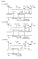
- Figs. 1(A), 1(B) and 1(C) are diagrams for explaining the construction of a FLOTOX EEPROM of a dual cell type according to one embodiment of the present invention. Particularly, Fig. 1(A) is a schematic sectional view. Fig. 1(B) is a sectional view taken along a line b-b in Fig. 1(A), and Fig. 1(C) is a sectional view taken along a line c-c in Fig. 1(A) .
- a cell structure of the EEPROM is provided in a surface portion of a p-type silicon substrate 21 isolated by a field oxide film (LOCOS oxide film) 22 formed in the surface portion of the p-type silicon substrate 21 by a LOCOS method.
- LOCOS oxide film field oxide film
- the cell structure includes a cell transistor 23 and a select transistor 24.
- the cell transistor 23 includes two paired floating gates 25a, 25b, a control gate 26 shared by the two floating gates 25a, 25b, and a single source 27 shared by the two floating gates 25a, 25b.
- the select transistor 24 includes a common drain 28, and a select gate 29 provided between the drain 28 and the two floating agates 25a, 25b.
- the select gate 29 includes a first band line 29a and a second band line 29b each extending in a direction in which the floating gates 25a, 25b are arranged.
- a portion of the first band line 29a associated with the floating gate 25a has a greater width
- a portion of the second band line 29b associated with the floating gate 25a has a smaller width.
- a portion of the first band line 29a associated with the floating gate 25b has a smaller width
- a portion of the second band line 29b associated with the floating gate 25b has a greater width.
- the two paired floating gates 25a, 25b are arranged generally perpendicularly to a direction extending between the drain 28 and the source 27.
- the source 27 and the drain 28 are shared by the two paired floating gates 25a, 25b. This reduces the size of the drain region 28, so that the drain region 28 can be spaced a predetermined distance 31 from a channel stopper region 30 provided below the LOCOS oxide film 22 for a higher breakdown voltage design.
- the drain region 28 of the select transistor 24 which requires the higher breakdown voltage design is shared by the two floating gates 25a, 25b, whereby the size of the drain region 28 is reduced as compared with a case in which the two cells are simply juxtaposed. Further, the cell area can be optimized by reducing the sizes of other portions of the two cells according to the breakdown voltage requirements.
- Tunnel windows 33a, 33b which are defined by smaller thickness portions of an insulating film 32 provided between the drain 28 and the two paired floating gates 25a, 25b, are respectively provided for the two paired floating gates 25a, 25b. Electrons are injected into and extracted from the floating gates 25a, 25b via the tunnel windows 33a, 33b.
- the paired floating gates 25a, 25b share the control gate 26.
- the select gate 29 including the two lines cooperates with the control gate 26 to select the floating gate 25a or 25b.
- the first band line 29a and the second band line 29b of the select gate 29 respectively have a greater gate length (greater width) portion and a smaller gate length (smaller width) portion in association with the floating gate 25a.
- the first band line 29a and the second band line 29b of the select gate 29 respectively have a smaller gate length (smaller width) portion and a greater gate length (greater width) portion in association with the floating gate 25b.
- a short channel effect can be intentionally provided on the smaller gate length portions, and the floating gates 25a, 25b can be individually operated by the other portions of the band lines of the select gate free from the short channel effect. That is, the floating gates 25a, 25b can be operated as independent cells.
- Figs. 2(A), 2 (B) and 2 (C) are schematic diagrams for explaining operations of the EEPROM of the dual cell structure shown in Figs. 1(A) to 1(C) .
- a higher voltage (15 to 17 V) is applied to the drain 28 and the select gate 29 (29a, 29b), and the control gate 26 and the silicon substrate 21 are kept at a GND level (ground potential). Further, the source 27 is opened. Thus, electrons are extracted from the floating gates 25a, 25b due to FN tunnel current.
- a higher voltage (15 to 17 V) is applied to the control gate 26 and the select gate 29 (29a, 29b), and the drain 28 and the silicon substrate 21 are kept at a GND level (ground potential). Further, the source 27 is opened. Thus, electrons are injected into the paired floating gates 25a, 25b from the drain 28 via the tunnel windows 33a, 33b.
- an operation voltage Vcc is applied to the drain 28 and the select gate 29 (29a, 29b).
- a sense voltage (a lower voltage, e.g., 1 to 3 V) is applied to the control gate 26, and the source 27 and the silicon substrate 21 are biased at a GND level (ground potential) for a read operation.
- the cell transistor 23 is held in an ON state or an OFF state, and data is read based on the state of the cell transistor 23.
- either one of the floating gates 25a, 25b is operated as an independent cell to read the data.
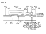
- the floating gate 25a shown in Figs. 1(A) to 1(C) is regarded as the independent cell from which the data is read, for example, the bias potentials of the source 27 and the silicon substrate 21 are kept at a GND level (ground potential) as shown in Fig. 3 . Further, an operation voltage Vcc is applied to the drain 28. Then, Vcc is applied to the first band line 29a, i.e., one 29a of the band lines of the select gate 29, and the second band line 29b, i.e., the other band line 29b of the select gate 29, is kept at 0 V. At this time, punch-through occurs below the second band line 29b, because the second band line 29b has a sufficiently small gate length.
- the current flow of the floating gate 25a is switched on and off by applying the operation voltage Vcc to the first band line 29a, i.e., the one band line 29a of the select gate 29, regardless of the potential (0 V) of the second band line 29b.
- the read operation can be performed by using either one of the paired floating gates 25a, 25b as the independent cell.
- the drain region 28 of the select transistor 24 which is required to have an area sufficient for the higher breakdown voltage design is shared by the two cells, whereby the drain region 28 has a sufficient breakdown voltage and yet has a minimum area.
- the select gate 29 includes the two band lines (the first band line 29a and the second band line 29b) having different widths, whereby the floating gates 25b, 25b each function as an independent cell.
- the p-type and n-type conductivities of the semiconductor members may be reversed.
- the direction of migration of the electrons is also reversed.
- the formation of the field oxide film may be achieved by an STI method rather than by the LOCOS method.
- Figs. 4(A), 4(B) and 4(C) are diagrams for explaining the construction of a FLOTOX EEPROM of the dual cell type according to another embodiment of the present invention. Particularly, Fig. 4(A) is a schematic plan view. Fig. 4(B) is a sectional view taken along a line b-b in Fig. 4(A), and Fig. 4(C) is a sectional view taken along a line c-c in Fig. 4(A) .
- a cell structure of the EEPROM is provided in a surface portion of a p-type silicon substrate 21 isolated by a field oxide film (LOCOS oxide film) 22 formed in the surface portion of the p-type silicon substrate 21 by the LOCOS method.
- the cell structure includes a cell transistor 23 and a select transistor 24.
- the cell transistor 23 includes two paired floating gates 25a, 25b and two sources 35a, 35b, which share a drain 28 provided in the select transistor 24.
- the two paired floating gates 25a, 25b are arranged generally perpendicularly to directions extending between the drain and the sources.
- drain region 28 This reduces the size of the drain region 28, so that the drain region 28 can be spaced a predetermined distance 31 from a channel stopper region 30 provided below the LOCOS oxide film 22 for a higher breakdown voltage design.
- Tunnel windows 33a, 33b which are defined by smaller thickness portions of an insulating film 32 provided between the drain 28 and the two paired floating gates 25a, 25b, are provided for the two paired floating gates 25a, 25b. Electrons are injected into and extracted from the floating gates 25a, 25b via the tunnel windows 33a, 33b.
- the paired floating gates 25a, 25b share a control gate 26. Further, the paired floating gates 25a, 25b share a select gate 34, which cooperates with the control gate 26 to select at least one of the two floating gates 25a, 25b.
- the sources 35a, 35b are respectively provided for the floating gates 25a, 25b.
- the EEPROM of the dual cell structure has a sufficient breakdown voltage and yet has a minimum area.
- the two floating gates 25a, 25b can be each driven as an independent cell from which the data is read.
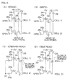
- Figs. 5(A), 5(B), 5(C) and 5(D) are circuit diagrams for explaining operations of the EEPROM of the dual cell structure shown in Figs. 4(A) to 4(C) .
- the operations of the EEPROM of the dual cell structure according to this embodiment will hereinafter be described.
- a higher voltage e.g., 15 to 17 V
- the drain 28 is kept at 0 V.
- the sources 35a, 35b are opened.
- electrons are injected into the paired floating gates 25a, 25b.
- a higher voltage e.g., 15 to 17 V
- the control gate 26 is kept at 0 V, and the sources 35a, 35b are opened.
- electrons are extracted from the paired floating gates 25a, 25b.
- an operation voltage e.g., a power supply voltage
- Vcc a lower voltage
- a lower voltage e.g., about 1 to about 2 V
- sense voltage a lower voltage
- current flowing from the drain 28 is detected with the sources 35a, 35b kept at a ground potential (GND).
- GND ground potential
- the voltage Vth of the cell transistor is lower than the sense voltage, so that the current flows.
- the voltage Vth of the cell transistor is higher than the sense voltage, so that the current does not flow.
- the data stored in the cells can be detected.
- test read operation is performed in the following manner.
- Vcc is applied to the select gate 34 and the drain 28, and the sense voltage is applied to the control gate 26.
- one of the sources 35a, 35b is opened, and the other source is kept at the ground potential (GND).
- GND ground potential
- the FLOTOX EEPROM of the dual cell type is provided, which is of a highly reliable design with a reduced cell area, and finds a wide range of applications.
- the p-type and n-type conductivities of the semiconductor members may be reversed.
- the direction of migration of the electrons is also reversed.
- the formation of the field oxide film may be achieved by an STI method rather than by the LOCOS method.
Landscapes
- Engineering & Computer Science (AREA)
- Microelectronics & Electronic Packaging (AREA)
- Non-Volatile Memory (AREA)
- Semiconductor Memories (AREA)
Applications Claiming Priority (3)
| Application Number | Priority Date | Filing Date | Title |
|---|---|---|---|
| JP2007018053A JP5252808B2 (ja) | 2007-01-29 | 2007-01-29 | Flotox型eeprom |
| JP2007051641A JP5073318B2 (ja) | 2007-03-01 | 2007-03-01 | Flotox型eeprom |
| PCT/JP2008/051213 WO2008093640A1 (ja) | 2007-01-29 | 2008-01-28 | Flotox型eeprom |
Publications (1)
| Publication Number | Publication Date |
|---|---|
| EP2109136A1 true EP2109136A1 (de) | 2009-10-14 |
Family
ID=39673951
Family Applications (1)
| Application Number | Title | Priority Date | Filing Date |
|---|---|---|---|
| EP08704022A Withdrawn EP2109136A1 (de) | 2007-01-29 | 2008-01-28 | Flotoxähnliches eeprom |
Country Status (6)
| Country | Link |
|---|---|
| US (1) | US8050105B2 (de) |
| EP (1) | EP2109136A1 (de) |
| KR (1) | KR20090106503A (de) |
| CN (1) | CN101595555A (de) |
| TW (1) | TW200845370A (de) |
| WO (1) | WO2008093640A1 (de) |
Cited By (1)
| Publication number | Priority date | Publication date | Assignee | Title |
|---|---|---|---|---|
| US8026545B2 (en) | 2008-12-01 | 2011-09-27 | Rohm Co., Ltd. | Eeprom |
Families Citing this family (3)
| Publication number | Priority date | Publication date | Assignee | Title |
|---|---|---|---|---|
| JP5112731B2 (ja) * | 2007-04-04 | 2013-01-09 | ローム株式会社 | Flotox型eeprom |
| US8320191B2 (en) | 2007-08-30 | 2012-11-27 | Infineon Technologies Ag | Memory cell arrangement, method for controlling a memory cell, memory array and electronic device |
| US8462553B2 (en) * | 2009-12-29 | 2013-06-11 | Aplus Flash Technology, Inc. | Cell array for highly-scalable, byte-alterable, two-transistor FLOTOX EEPROM non-volatile memory |
Family Cites Families (6)
| Publication number | Priority date | Publication date | Assignee | Title |
|---|---|---|---|---|
| US5471422A (en) * | 1994-04-11 | 1995-11-28 | Motorola, Inc. | EEPROM cell with isolation transistor and methods for making and operating the same |
| JP4183290B2 (ja) | 1994-12-27 | 2008-11-19 | マクロニクス インターナショナル カンパニイ リミテッド | ベリファイ機能を備えた不揮発性半導体装置 |
| JP3023321B2 (ja) * | 1997-03-10 | 2000-03-21 | 株式会社東芝 | 不揮発性半導体記憶装置 |
| JP3023330B2 (ja) * | 1997-06-10 | 2000-03-21 | 株式会社東芝 | 不揮発性半導体記憶装置 |
| JP4530464B2 (ja) * | 2000-03-09 | 2010-08-25 | ルネサスエレクトロニクス株式会社 | 半導体集積回路 |
| JP2005020349A (ja) * | 2003-06-26 | 2005-01-20 | Renesas Technology Corp | 半導体集積回路および電子システム |
-
2008
- 2008-01-28 WO PCT/JP2008/051213 patent/WO2008093640A1/ja not_active Ceased
- 2008-01-28 US US12/449,169 patent/US8050105B2/en not_active Expired - Fee Related
- 2008-01-28 EP EP08704022A patent/EP2109136A1/de not_active Withdrawn
- 2008-01-28 KR KR1020097013987A patent/KR20090106503A/ko not_active Withdrawn
- 2008-01-28 CN CNA2008800032096A patent/CN101595555A/zh active Pending
- 2008-01-29 TW TW097103291A patent/TW200845370A/zh unknown
Non-Patent Citations (1)
| Title |
|---|
| See references of WO2008093640A1 * |
Cited By (2)
| Publication number | Priority date | Publication date | Assignee | Title |
|---|---|---|---|---|
| US8026545B2 (en) | 2008-12-01 | 2011-09-27 | Rohm Co., Ltd. | Eeprom |
| US9059034B2 (en) | 2008-12-01 | 2015-06-16 | Rohm Co., Ltd. | Eeprom |
Also Published As
| Publication number | Publication date |
|---|---|
| TW200845370A (en) | 2008-11-16 |
| WO2008093640A1 (ja) | 2008-08-07 |
| KR20090106503A (ko) | 2009-10-09 |
| US8050105B2 (en) | 2011-11-01 |
| CN101595555A (zh) | 2009-12-02 |
| US20100002524A1 (en) | 2010-01-07 |
Similar Documents
| Publication | Publication Date | Title |
|---|---|---|
| US9812212B2 (en) | Memory cell with low reading voltages | |
| US7974127B2 (en) | Operation methods for memory cell and array for reducing punch through leakage | |
| US5301150A (en) | Flash erasable single poly EPROM device | |
| US7755135B2 (en) | EEPROM having single gate structure | |
| US7177192B2 (en) | Method of operating a flash memory device | |
| JP2005510889A (ja) | バイト消去可能なeepromメモリを有する半導体デバイス | |
| US8432186B1 (en) | Programmable logic switch | |
| US9935117B2 (en) | Single poly nonvolatile memory cells, arrays thereof, and methods of operating the same | |
| US20090268527A1 (en) | Sonos memory device and method of operating a sonos memory device | |
| KR20050085268A (ko) | 비휘발성 메모리 셀을 프로그램하기 위한 개선된 시스템 | |
| US8050105B2 (en) | FLOTOX-type EEPROM | |
| US6914819B2 (en) | Non-volatile flash memory | |
| JP2008182232A (ja) | 不揮発性メモリ素子及びその動作方法 | |
| US7483310B1 (en) | System and method for providing high endurance low cost CMOS compatible EEPROM devices | |
| JP5252808B2 (ja) | Flotox型eeprom | |
| JP2009094479A (ja) | 不揮発性メモリ装置及びその動作方法 | |
| US7969790B2 (en) | Method of erasing an NVM cell that utilizes a gated diode | |
| US20230200062A1 (en) | Semiconductor device | |
| US8072807B2 (en) | FLOTOX type EEPROM | |
| JP5073318B2 (ja) | Flotox型eeprom | |
| JPH02218158A (ja) | 不揮発性半導体メモリ装置 | |
| KR20140119577A (ko) | 싱글 폴리형 이이피롬의 셀 어레이 및 그 동작방법 | |
| JP5502314B2 (ja) | Eeprom | |
| JP2013077780A (ja) | 半導体記憶装置及び半導体記憶素子 | |
| US20100259996A1 (en) | System and method for providing low cost high endurance low voltage electrically erasable programmable read only memory |
Legal Events
| Date | Code | Title | Description |
|---|---|---|---|
| PUAI | Public reference made under article 153(3) epc to a published international application that has entered the european phase |
Free format text: ORIGINAL CODE: 0009012 |
|
| 17P | Request for examination filed |
Effective date: 20090709 |
|
| AK | Designated contracting states |
Kind code of ref document: A1 Designated state(s): AT BE BG CH CY CZ DE DK EE ES FI FR GB GR HR HU IE IS IT LI LT LU LV MC MT NL NO PL PT RO SE SI SK TR |
|
| DAX | Request for extension of the european patent (deleted) | ||
| STAA | Information on the status of an ep patent application or granted ep patent |
Free format text: STATUS: THE APPLICATION HAS BEEN WITHDRAWN |
|
| 18W | Application withdrawn |
Effective date: 20110103 |