EP2105952A2 - Tiefes reaktives Ionenätzen - Google Patents
Tiefes reaktives Ionenätzen Download PDFInfo
- Publication number
- EP2105952A2 EP2105952A2 EP09156284A EP09156284A EP2105952A2 EP 2105952 A2 EP2105952 A2 EP 2105952A2 EP 09156284 A EP09156284 A EP 09156284A EP 09156284 A EP09156284 A EP 09156284A EP 2105952 A2 EP2105952 A2 EP 2105952A2
- Authority
- EP
- European Patent Office
- Prior art keywords
- etch
- pressure
- sample
- cycle
- mtorr
- Prior art date
- Legal status (The legal status is an assumption and is not a legal conclusion. Google has not performed a legal analysis and makes no representation as to the accuracy of the status listed.)
- Withdrawn
Links
Images




Classifications
-
- H—ELECTRICITY
- H10—SEMICONDUCTOR DEVICES; ELECTRIC SOLID-STATE DEVICES NOT OTHERWISE PROVIDED FOR
- H10P—GENERIC PROCESSES OR APPARATUS FOR THE MANUFACTURE OR TREATMENT OF DEVICES COVERED BY CLASS H10
- H10P50/00—Etching of wafers, substrates or parts of devices
- H10P50/20—Dry etching; Plasma etching; Reactive-ion etching
- H10P50/24—Dry etching; Plasma etching; Reactive-ion etching of semiconductor materials
- H10P50/242—Dry etching; Plasma etching; Reactive-ion etching of semiconductor materials of Group IV materials
- H10P50/244—Dry etching; Plasma etching; Reactive-ion etching of semiconductor materials of Group IV materials comprising alternated and repeated etching and passivation steps
Definitions
- This invention relates to anisotropic etching of substrates, and in particular deep reactive ion etching.
- etching cycle RF power is applied on the substrate to generate an electric field that causes ion bombardment on the bottom of the etch feature (cavity or trench). This removes the polymer only on the bottom of the etch feature and not on the sidewalls. Repeating alternate etching and deposition phases generates an anisotropic etched feature.
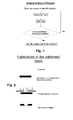
- Fig. 1 shows the sequence diagram of the standard Bosch Process.
- the Bosch process normally uses pressure between 5 and 100mTorr.
- the etch rate is the main concern for productivity purposes, and sidewall roughness is acceptable to some extent
- increasing the pressure above 100mTorr and increasing the ratio between etching time and deposition time are both solutions to achieving a higher etch rate with the same equipment (generally an Inductively Coupled Plasma System).
- DRIE Deep Reactive Ion Etching
- grass This also generates non-uniformities across the wafer because the roughness is rarely uniform across the wafer. This roughness also causes unwanted sidewall roughness.
- FIG. 2 shows an example of how to make the patterned mask.
- a silicon wafer substrate is normally used.
- a photoresist is dispensed on top of the wafer using spin coating technique.
- a quartz plate with a pattern made of metal on top of it is placed between a shining light and the substrate. Regions in the photoresist where the light reaches the substrate get altered and become soluble.
- the wafer is then immersed in a liquid (a developer) that can dissolve selectively these altered regions. What is left is an image made of photoresist that is identical to the metal pattern that was on the quartz plate.
- the outcome of these steps is the sample that is used for anisotropic etching (entered in the ICP chamber in Fig.1 ).
- Fig. 3 is a schematic representation of a cross-section of the sample in a standard Bosch process during the three key moments of the first cycle. In order from top to bottom: at the end of the deposition showing the substrate 10, the photoresist 12, and the polymer layer 14, during the etch step after the polymer 14 is completely removed from the bottom, and at the end of the etch step showing the resulting partly formed trench 16a.
- Fig. 4 shows a schematic representation of the steps that the sample encounters during the second cycle of the sequence shown in Fig.1 when the answer to the question after the first cycle is "NO". This is called the first scallop of the etching.
- the trench is further extended as shown at 16b.
- Fig.5 shows a schematic representation of the steps that the sample encounters during the third cycle of the sequence shown in Fig.1 the answer to the question after the second cycle is "NO".
- Fig. 6 shows the sample after 7 cycles of Standard Bosch Process when successive trench portions 16a to 16n are formed after each cycle. This is repeated until the right depth is obtained. The result is an anisotropic etched feature.
- etch pressure between 1 to 40mTorr.
- etch rate between 1 to 40mTorr.
- Fig. 7 is a sequence diagram of the 3-step method from STS using high pressure.
- Fig. 8 shows a schematic representation of the steps that the sample encounters during the first cycle of the sequence shown in Fig. 7 . Roughness is observed when using high pressure.
- Fig. 9 is a schematic representation of the steps that the sample encounters during the second cycle of the sequence shown in Fig. 7 when answering "NO" at the question after the first cycle.
- Fig. 10 is a schematic representation of the steps that the sample encounters during the third cycle of the sequence shown in Fig. 7 when answering "NO" at the question after the second cycle.
- a method of performing an anisotropic etch on a substrate in an inductively coupled plasma etch chamber comprising performing at least three cycles of a procedure consisting essentially of the four following steps:
- the platen power in the inductively coupled plasma etch chamber is greater for steps b and d than for step c and the pressure in step d is less than the pressure in step b .
- the substrate is silicon.
- the protective polymer is deposited using C 4 F 8 gas, and the etchant gas is selected from the group consisting of SF 6 , O 2 and a combination thereof.
- the Radio Frequency (RF) coil matching network unit needs to be able to react to the fast change of plasma conditions. Reducing the pressure rapidly corresponds to a fast change in impedance and therefore the matching network unit needs to react fast on such changes.
- the addition of an extra bombardment step reduces the mask selectivity.
- Fig. 1 is a sequence diagram of the standard Bosch process
- Fig. 2 is a schematic representation in cross-section of the photolithography process normally used to make the patterned mask
- Fig. 3 is a schematic representation of the cross-section of the sample under a standard Bosch process during the 3 key moments of the first cycle. In order from top to bottom: at the end of the deposition, during the etch step after the polymer is completely removed from the bottom, and at the end of the etch step;
- Fig. 4 is a schematic representation of the cross-section of the sample under a standard Bosch process during the 3 key moments of the first cycle. In order from top to bottom: at the end of the deposition, during the etch step after the polymer is completely removed from the bottom, and at the end of the etch step;
- Fig. 5 is a schematic representation of the cross-section of the sample under a standard Bosch process during the 3 key moments of the first cycle. In order from top to bottom: at the end of the deposition, during the etch step after the polymer is completely removed from the bottom, and at the end of the etch step;
- Fig.6 is a schematic representation of the cross-section of the sample under a standard Bosch process after 7 cycles
- Fig. 7 is a sequence diagram of the 3 step STS modified Bosch Process
- Fig. 8 is a schematic representation of the cross-section of the sample under 3-step Bosch Process during the 3 key moments of the first cycle. In order from top to bottom: at the end of the deposition, during the etch step after the polymer is completely removed from the bottom, and at the end of the etch step;
- Fig. 9 is a schematic representation of the cross-section of the sample under 3-step Bosch Process during the 3 key moments of the second cycle. In order from top to bottom: at the end of the deposition, during the etch step after the polymer is completely removed from the bottom, and at the end of the etch step;
- Fig. 10 is a schematic representation of the cross-section of the sample under 3-step Bosch Process during the 3 key moments of the third cycle. In order from top to bottom: at the end of the deposition, during the etch step after the polymer is completely removed from the bottom, and at the end of the etch step;
- Fig. 11 is a sequence diagram of the invention of a four step process in accordance with an embodiment of the invention.
- Fig. 12 is a schematic representation of the cross-section of the sample under 4-step process in accordance with an embodiment of the invention during the four key moments of the first cycle.
- etch step at the end of the deposition, during the etch step after the polymer is completely removed from the bottom, and at the end of the etch step;
- Fig. 13 is a schematic representation of the cross-section of the sample under 4-step process in accordance with an embodiment of the invention during the 3 key moments of the second cycle.
- etch step at the end of the deposition, during the etch step after the polymer is completely removed from the bottom, and at the end of the etch step;
- Fig. 14 is a schematic representation of the cross-section of the sample under 4-step process during the 3 key moments of the third cycle. In order from top to bottom: at the end of the deposition, during the etch step after the polymer is completely removed from the bottom, and at the end of the etch step;
- Fig. 15 is a SEM micrograph of a cavity on the center of the Sample A. Top: Whole cross-section of the square cavity. Bottom left: Focus on the back wall. Bottom right: Zoom of the photoresist mask and the etch undercut;
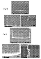
- Fig. 16 is a SEM micrograph of a cavity on the top (opposite to major flat) of the Sample A.
- Top Whole cross-section of the square cavity.
- Bottom left Focus on the back wall.
- Bottom right Zoom of the photoresist mask and the etch undercut;
- Fig. 17 is a SEM micrograph of a cavity on the right hand side (considering the major flat on the bottom) of the Sample A. Top: Whole cross-section of the square cavity. Bottom left: Focus on the back wall. Bottom right: Zoom of the photoresist mask and the etch undercut;
- Fig. 18 is a SEM micrograph of a cavity on the center of the Sample B. Top: Whole cross-section of the square cavity. Bottom left: Focus on the back wall. Bottom right: Zoom of the photoresist mask and the etch undercut;
- Fig. 19 is a SEM micrograph of a cavity on the top (opposite to major flat) of the Sample B.
- Top Whole cross-section of the square cavity.
- Bottom left Focus on the back wall.
- Bottom right Zoom of the photoresist mask and the etch undercut.
- Fig. 20 SEM micrograph of a cavity on the right hand side (considering the major flat on the bottom) of the Sample B. Top: Whole cross-section of the square cavity. Bottom left: Focus on the back wall. Bottom right: Zoom of the photoresist mask and the etch undercut;
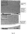
- Fig. 21 is a comparison of wall roughness between Fig 17 (above from Sample A) and Fig. 20 (below from Sample B) on the same site on each sample.
- the inlet of each image shows the whole cross-section;
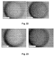
- Fig. 22 is a microscope image on the two worst dice of the wafer in term of roughness for the Sample A.
- Left hand side image Top of the wafer.
- Right hand side Right of the wafer;
- Fig. 23 is a microscope image on the two worst dice of the wafer in term of roughness for the Sample B.
- Left hand side image Top of the wafer.
- Right hand side Right of the wafer;
- Fig. 24 shows the measured dimensions on SEM micrograph for the evaluation of the profile angle.
- the inlet shows a diagram of the shape at the bottom of a square cavity.
- the 3 black lines show 3 possible cross-section lines;
- Fig. 25 shows the measured dimensions on SEM micrograph for the evaluation of the profile angle of the back wall.
- the inlet shows a diagram of the shape at the bottom of a square cavity.
- the black line shows the plan in which the measurement is done;
- Fig. 26 shows the measured dimensions on SEM micrograph for the photoresist end thickness, the undercut and the scallop size.
- FIG 11 shows a sequence diagram in accordance with an embodiment of the present invention.
- the sample is placed in the ICP chamber.
- the plasma is then lit, and the sample undergoes a deposition, followed by the etching step that removes the deposition.
- a high pressure etching main etch
- the cycle finishes with another bombardment condition at low pressure and high platen power prior to the next cycle, making a total of four steps per cycle. These four steps are repeated until the right depth is obtained or if an underneath etch stop layer is reached.
- Fig. 12 is a schematic representation of the steps that the sample encounters during the first cycle of the sequence shown in Fig. 11 .
- the polymer is deposited as explained with reference to Figure 3 .
- This polymer is removed in the second step at least from the surface of the photoresist and the bottom of the opening in the photoresist layer 12. The polymer may remain on the sidewalls, but this remaining layer is not shown in the drawings.
- the high pressure etch is performed to form the first portion 16a of the trench, and then the fourth step is performed to remove any surface roughness.
- Figure 13 shows the formation of the second portion 16b of the trench in the third step. This is formed with surface roughness 18, which is removed in the fourth step before starting the third cycle as shown in Figure 14 .
- Figures 13 and 14 schematize the 4-step method when using high pressure in the main etch step for subsequent cycles 2 and 3. At the end of the high pressure main etch step in each cycle, roughness is observed as in the case of the 3-step method. The roughness removal step then smoothes the surface.
- the following images show Scanning Electron Microscopy (SEM) images coming from a few sites on Sample A.
- Fig. 15 is a SEM micrograph of a cavity on the center of the Sample A. Top: Whole cross-section of the square cavity. Bottom left: Focus on the back wall. Bottom right: Zoom of the photoresist mask and the etch undercut.
- Fig. 16 is a SEM micrograph of a cavity on the top (opposite to major flat) of the Sample A.
- Top Whole cross-section of the square cavity.
- Bottom left Focus on the back wall.
- Bottom right Zoom of the photoresist mask and the etch undercut.
- Fig. 17 is a SEM micrograph of a cavity on the right hand side (considering the major flat on the bottom) of the Sample A. Top: Whole cross-section of the square cavity. Bottom left: Focus on the back wall. Bottom right: Zoom of the photoresist mask and the etch undercut.
- Figs. 18 to 20 are Scanning Electron Microscopy (SEM) images coming from a few sites on Sample B. The same sites as Sample A were observed.
- Fig. 18 is a SEM micrograph of a cavity on the center of the Sample B. Top: Whole cross-section of the square cavity. Bottom left: Focus on the back wall. Bottom right: Zoom of the photoresist mask and the etch undercut.
- Fig. 19 is a SEM micrograph of a cavity on the top (opposite to major flat) of the Sample B.
- Top Whole cross-section of the square cavity.
- Bottom left Focus on the back wall.
- Bottom right Zoom of the photoresist mask and the etch undercut.
- Fig. 20 is a SEM micrograph of a cavity on the right hand side (considering the major flat on the bottom) of the Sample B. Top: Whole cross-section of the square cavity. Bottom left: Focus on the back wall. Bottom right: Zoom of the photoresist mask and the etch undercut.
- Fig. 21 shows a comparison of the wall roughness for the same site on each sample (right hand side of the wafer).
- Sample A above image
- Sample B bottom image
- Sample A recipe will be limited at some depth because sidewall and bottom roughness will worsen as the etch gets deeper.
- Sample B recipe does not show limitation yet at this depth.
- these vertical lines seen in Sample A demonstrate limitation in depth for such recipe for some commercial applications where sidewall roughness is specified tightly.
- This also demonstrates that this recipe has a maximum limit in depth for which it can be used. Roughness can only get worse with the same recipe and eventually, "grass" will appear if we etch further down.
- Sample B recipe does not show such limitations; therefore that recipe is less sensitive to generate grass. Therefore, for the same specification in roughness, the Sample B recipe will be limited at a depth that is greater than for the Sample A recipe.
- the Sample A recipe would have to be modified in order to meet tight specification, and necessarily, the etch rate would be lowered to accommodate smoother sidewalls and smoother bottom surfaces. Either pressure, total time of a Bosch cycle, or the etch-to-deposition ratio would be reduced. Both would result in lower etch rates.
- Figs. 22 and Fig. 23 are microscope images at 10X, on the roughest die on two regions for both wafer (the two worst regions). The same dice were compared on both wafers. The focus is on the bottom of the cavity. We observe that Sample B has slightly less roughness on the bottom compared to Sample A.
- Fig. 22 is a microscope image on the two worst dice of the wafer in term of roughness for the Sample A. Left hand side image: Top of the wafer. Right hand side: Right of the wafer.
- Fig. 23 is a microscope image on the two worst dice of the wafer in term of roughness for the Sample B. Left hand side image: Top of the wafer. Right hand side: Right of the wafer.
- Fig. 25 shows the dimensions we measured to evaluate the profile angle. This is the standard way to measure the profile angle in the DRIE field.
- Fig. 24 depicts the shape of the bottom of the cavity for a square mask opening when the profile is re-entrant (i.e. profile angle > 90°).
- profile angle > 90° The cleavage of such structure is difficult and the position of the cross-section line will vary from one to another. Therefore the profile angle evaluated in Table 4.2.3 is only indicative and no uniformity was evaluated.
- Fig.25 shows the measured dimensions used to measure the profile angle of the back wall. The same Equation 2 was used. This measurement does not depend on the cross-section line and is therefore reproducible form one to another. This measure was used to compare objectively the two profiles. We observe that the averages are identical but that less variation is observe across the wafer for Sample B. This can be potentially explained with the fact that Sample B recipe well clears the roughness on the bottom of the cavity up to the corner of the cavity at each cycle.
- Fig. 24 shows the measured dimensions on SEM micrograph for the evaluation of the profile angle.
- the inset shows a diagram of the shape at the bottom of a square cavity.
- the three lines show three possible cross-section lines.
- Fig. 25 shows the measured dimensions on SEM micrograph for the evaluation of the profile angle of the back wall.
- the inset shows a diagram of the shape at the bottom of a square cavity.
- the red line shows the plan in which the measurement is done.
- Fig 26 shows the dimensions where we measured the photoresist end thickness, the undercut and the scallop size.
- the undercut is the distance between the opening of the photoresist mask and the lateral edge of the first scallop.
- the Sample A undercut shows less uniform undercut across the wafer. It is not sure at this point if this is due to the fourth step on the first cycle.
- the scallop size is the horizontal dimension of the second scallop. We measure this particular scallop because the scallops tend to diminish in size as the etch goes deeper. Therefore this scallop is assumed to be the largest on each cavity. This value is identical on both samples. This dimension mainly depend on the high pressure etch step. Since this step is identical in both recipes, it is normal to find the same result.
- Equation 3 we used the average depth of the cavity, an initial thickness of 10 ⁇ 0.1 ⁇ m (guarantied specification for this photolithography manufactured mask), and the minimum end thickness found on each wafer. Therefore this selectivity is the worst case found in all measurements. The fact that Sample B has a lower selectivity was expected since more ion bombardment is used at each cycle. However, selectivity greater than 100:1 is generally considered in the industry as out standing for such etching.
- Embodiments of the present invention when compared to the 3-step method results in a similar profile angle, a similar etch rate, the same scallop size, and a similar undercut.
- Embodiments of the present invention also prevent the worsening of the bottom roughness, and therefore allow the use of high pressure without its associated disadvantages. It also pushes further the theoretical limit of the maximum depth that can be achieved with the standard Bosch process.
Landscapes
- Drying Of Semiconductors (AREA)
Applications Claiming Priority (1)
| Application Number | Priority Date | Filing Date | Title |
|---|---|---|---|
| US3991208P | 2008-03-27 | 2008-03-27 |
Publications (2)
| Publication Number | Publication Date |
|---|---|
| EP2105952A2 true EP2105952A2 (de) | 2009-09-30 |
| EP2105952A3 EP2105952A3 (de) | 2010-10-20 |
Family
ID=40790642
Family Applications (1)
| Application Number | Title | Priority Date | Filing Date |
|---|---|---|---|
| EP09156284A Withdrawn EP2105952A3 (de) | 2008-03-27 | 2009-03-26 | Tiefes reaktives Ionenätzen |
Country Status (2)
| Country | Link |
|---|---|
| US (1) | US20090242512A1 (de) |
| EP (1) | EP2105952A3 (de) |
Families Citing this family (14)
| Publication number | Priority date | Publication date | Assignee | Title |
|---|---|---|---|---|
| KR101867998B1 (ko) * | 2011-06-14 | 2018-06-15 | 삼성전자주식회사 | 패턴 형성 방법 |
| US9267605B2 (en) | 2011-11-07 | 2016-02-23 | Lam Research Corporation | Pressure control valve assembly of plasma processing chamber and rapid alternating process |
| US20130203259A1 (en) * | 2012-02-07 | 2013-08-08 | Lam Research Corporation | Pressure control valve assembly of plasma processing chamber and rapid alternating process |
| US9679751B2 (en) | 2012-03-15 | 2017-06-13 | Lam Research Corporation | Chamber filler kit for plasma etch chamber useful for fast gas switching |
| JP6173086B2 (ja) * | 2013-07-19 | 2017-08-02 | キヤノン株式会社 | シリコン基板のエッチング方法 |
| JP6456049B2 (ja) * | 2014-06-16 | 2019-01-23 | キヤノン株式会社 | 貫通基板の形成方法 |
| EP3012857A1 (de) | 2014-10-21 | 2016-04-27 | ams AG | Verfahren zur Herstellung einer Öffnung mit glatter vertikaler Seitenwand in einem Halbleitersubstrat |
| US9997364B2 (en) * | 2016-10-19 | 2018-06-12 | Lam Research Corporation | High aspect ratio etch |
| CN108573867B (zh) * | 2017-03-13 | 2020-10-16 | 北京北方华创微电子装备有限公司 | 硅深孔刻蚀方法 |
| CN109218945A (zh) * | 2018-08-07 | 2019-01-15 | 瑞声科技(新加坡)有限公司 | Mems结构的制造方法、mems结构及硅麦克风 |
| CN109767980B (zh) * | 2019-01-22 | 2021-07-30 | 上海华虹宏力半导体制造有限公司 | 超级结及其制造方法、超级结的深沟槽制造方法 |
| JP2020122740A (ja) * | 2019-01-31 | 2020-08-13 | セイコーエプソン株式会社 | 構造体形成方法およびデバイス |
| JP7853127B2 (ja) * | 2022-03-16 | 2026-04-28 | 株式会社ディスコ | チップの製造方法 |
| CN118280922B (zh) * | 2024-05-29 | 2025-04-29 | 浙江创芯集成电路有限公司 | 半导体结构的形成方法 |
Citations (2)
| Publication number | Priority date | Publication date | Assignee | Title |
|---|---|---|---|---|
| US5501893A (en) | 1992-12-05 | 1996-03-26 | Robert Bosch Gmbh | Method of anisotropically etching silicon |
| US6127273A (en) | 1996-10-07 | 2000-10-03 | Robert Bosch Gmbh | Process for anisotropic plasma etching of different substrates |
Family Cites Families (5)
| Publication number | Priority date | Publication date | Assignee | Title |
|---|---|---|---|---|
| US5972235A (en) * | 1997-02-28 | 1999-10-26 | Candescent Technologies Corporation | Plasma etching using polycarbonate mask and low pressure-high density plasma |
| JP2991177B2 (ja) * | 1997-12-15 | 1999-12-20 | 日本電気株式会社 | 半導体装置の製造方法 |
| FR2834382B1 (fr) * | 2002-01-03 | 2005-03-18 | Cit Alcatel | Procede et dispositif de gravure anisotrope du silicium a haut facteur d'aspect |
| US6846746B2 (en) * | 2002-05-01 | 2005-01-25 | Applied Materials, Inc. | Method of smoothing a trench sidewall after a deep trench silicon etch process |
| US7359177B2 (en) * | 2005-05-10 | 2008-04-15 | Applied Materials, Inc. | Dual bias frequency plasma reactor with feedback control of E.S.C. voltage using wafer voltage measurement at the bias supply output |
-
2009
- 2009-03-24 US US12/409,699 patent/US20090242512A1/en not_active Abandoned
- 2009-03-26 EP EP09156284A patent/EP2105952A3/de not_active Withdrawn
Patent Citations (2)
| Publication number | Priority date | Publication date | Assignee | Title |
|---|---|---|---|---|
| US5501893A (en) | 1992-12-05 | 1996-03-26 | Robert Bosch Gmbh | Method of anisotropically etching silicon |
| US6127273A (en) | 1996-10-07 | 2000-10-03 | Robert Bosch Gmbh | Process for anisotropic plasma etching of different substrates |
Also Published As
| Publication number | Publication date |
|---|---|
| EP2105952A3 (de) | 2010-10-20 |
| US20090242512A1 (en) | 2009-10-01 |
Similar Documents
| Publication | Publication Date | Title |
|---|---|---|
| US20090242512A1 (en) | Deep reactive ion etching | |
| US9224615B2 (en) | Noble gas bombardment to reduce scallops in bosch etching | |
| US5354417A (en) | Etching MoSi2 using SF6, HBr and O2 | |
| US6380095B1 (en) | Silicon trench etch using silicon-containing precursors to reduce or avoid mask erosion | |
| US7829465B2 (en) | Method for plasma etching of positively sloped structures | |
| CN111243951B (zh) | 一种深硅刻蚀方法 | |
| US11854817B2 (en) | Manufacturing method for deep trench capacitor with scalloped profile | |
| EP1042796A1 (de) | Verbesserte methode eine oxidschicht zu ätzen | |
| JPH1092798A (ja) | 単結晶シリコンのエッチング方法 | |
| EP2022106A2 (de) | Verfahren zur minimierung von masken-unterschnitten und -kerben für ein plasmaverarbeitungssystem | |
| JPH11354499A (ja) | コンタクトホール等の形成方法 | |
| JP2004304029A (ja) | プラズマ処理方法 | |
| EP4649526A1 (de) | Verfahren zur herstellung eines supraleitenden durchgangs durch einen halbleiterwafer | |
| US6900136B2 (en) | Method for reducing reactive ion etching (RIE) lag in semiconductor fabrication processes | |
| US6540885B1 (en) | Profile control of oxide trench features for dual damascene applications | |
| CN108133888B (zh) | 一种深硅刻蚀方法 | |
| US20210159082A1 (en) | Protective layers and methods of formation during plasma etching processes | |
| US6117764A (en) | Use of a plasma source to form a layer during the formation of a semiconductor device | |
| EP2579299B1 (de) | Plasmaätzverfahren | |
| US5908320A (en) | High selectivity BPSG:TiSi2 contact etch process | |
| Selamoglu et al. | Tapered etching of aluminum with CHF3/Cl2/BCl3 and its impact on step coverage of plasma‐deposited silicon oxide from tetraethoxysilane | |
| EP4202979A1 (de) | Verfahren zur verminderung der oberflächenrauheit | |
| US20240234157A9 (en) | Polymer Removal via Multiple Flash Steps during Plasma Etch | |
| JP2011211135A (ja) | プラズマ処理方法 | |
| WO2000029640A1 (en) | Method for residue-free anisotropic etching of aluminum and its alloys |
Legal Events
| Date | Code | Title | Description |
|---|---|---|---|
| PUAI | Public reference made under article 153(3) epc to a published international application that has entered the european phase |
Free format text: ORIGINAL CODE: 0009012 |
|
| AK | Designated contracting states |
Kind code of ref document: A2 Designated state(s): AT BE BG CH CY CZ DE DK EE ES FI FR GB GR HR HU IE IS IT LI LT LU LV MC MK MT NL NO PL PT RO SE SI SK TR |
|
| AX | Request for extension of the european patent |
Extension state: AL BA RS |
|
| PUAL | Search report despatched |
Free format text: ORIGINAL CODE: 0009013 |
|
| AK | Designated contracting states |
Kind code of ref document: A3 Designated state(s): AT BE BG CH CY CZ DE DK EE ES FI FR GB GR HR HU IE IS IT LI LT LU LV MC MK MT NL NO PL PT RO SE SI SK TR |
|
| AX | Request for extension of the european patent |
Extension state: AL BA RS |
|
| 17P | Request for examination filed |
Effective date: 20110416 |
|
| AKX | Designation fees paid |
Designated state(s): AT BE BG CH CY CZ DE DK EE ES FI FR GB GR HR HU IE IS IT LI LT LU LV MC MK MT NL NO PL PT RO SE SI SK TR |
|
| RAP1 | Party data changed (applicant data changed or rights of an application transferred) |
Owner name: TELEDYNE DALSA SEMICONDUCTOR INC. |
|
| STAA | Information on the status of an ep patent application or granted ep patent |
Free format text: STATUS: THE APPLICATION IS DEEMED TO BE WITHDRAWN |
|
| 18D | Application deemed to be withdrawn |
Effective date: 20121002 |