EP2081229A2 - Solid-state imaging device, method of fabricating solid-state imaging device - Google Patents
Solid-state imaging device, method of fabricating solid-state imaging device Download PDFInfo
- Publication number
- EP2081229A2 EP2081229A2 EP09000727A EP09000727A EP2081229A2 EP 2081229 A2 EP2081229 A2 EP 2081229A2 EP 09000727 A EP09000727 A EP 09000727A EP 09000727 A EP09000727 A EP 09000727A EP 2081229 A2 EP2081229 A2 EP 2081229A2
- Authority
- EP
- European Patent Office
- Prior art keywords
- imaging device
- film
- state imaging
- solid
- opening
- Prior art date
- Legal status (The legal status is an assumption and is not a legal conclusion. Google has not performed a legal analysis and makes no representation as to the accuracy of the status listed.)
- Granted
Links
Images







Classifications
-
- H—ELECTRICITY
- H10—SEMICONDUCTOR DEVICES; ELECTRIC SOLID-STATE DEVICES NOT OTHERWISE PROVIDED FOR
- H10F—INORGANIC SEMICONDUCTOR DEVICES SENSITIVE TO INFRARED RADIATION, LIGHT, ELECTROMAGNETIC RADIATION OF SHORTER WAVELENGTH OR CORPUSCULAR RADIATION
- H10F39/00—Integrated devices, or assemblies of multiple devices, comprising at least one element covered by group H10F30/00, e.g. radiation detectors comprising photodiode arrays
- H10F39/011—Manufacture or treatment of image sensors covered by group H10F39/12
- H10F39/026—Wafer-level processing
-
- H—ELECTRICITY
- H10—SEMICONDUCTOR DEVICES; ELECTRIC SOLID-STATE DEVICES NOT OTHERWISE PROVIDED FOR
- H10F—INORGANIC SEMICONDUCTOR DEVICES SENSITIVE TO INFRARED RADIATION, LIGHT, ELECTROMAGNETIC RADIATION OF SHORTER WAVELENGTH OR CORPUSCULAR RADIATION
- H10F39/00—Integrated devices, or assemblies of multiple devices, comprising at least one element covered by group H10F30/00, e.g. radiation detectors comprising photodiode arrays
- H10F39/10—Integrated devices
- H10F39/12—Image sensors
-
- H—ELECTRICITY
- H10—SEMICONDUCTOR DEVICES; ELECTRIC SOLID-STATE DEVICES NOT OTHERWISE PROVIDED FOR
- H10F—INORGANIC SEMICONDUCTOR DEVICES SENSITIVE TO INFRARED RADIATION, LIGHT, ELECTROMAGNETIC RADIATION OF SHORTER WAVELENGTH OR CORPUSCULAR RADIATION
- H10F39/00—Integrated devices, or assemblies of multiple devices, comprising at least one element covered by group H10F30/00, e.g. radiation detectors comprising photodiode arrays
- H10F39/10—Integrated devices
- H10F39/12—Image sensors
- H10F39/199—Back-illuminated image sensors
-
- H—ELECTRICITY
- H10—SEMICONDUCTOR DEVICES; ELECTRIC SOLID-STATE DEVICES NOT OTHERWISE PROVIDED FOR
- H10F—INORGANIC SEMICONDUCTOR DEVICES SENSITIVE TO INFRARED RADIATION, LIGHT, ELECTROMAGNETIC RADIATION OF SHORTER WAVELENGTH OR CORPUSCULAR RADIATION
- H10F39/00—Integrated devices, or assemblies of multiple devices, comprising at least one element covered by group H10F30/00, e.g. radiation detectors comprising photodiode arrays
- H10F39/80—Constructional details of image sensors
- H10F39/805—Coatings
- H10F39/8057—Optical shielding
-
- H—ELECTRICITY
- H10—SEMICONDUCTOR DEVICES; ELECTRIC SOLID-STATE DEVICES NOT OTHERWISE PROVIDED FOR
- H10F—INORGANIC SEMICONDUCTOR DEVICES SENSITIVE TO INFRARED RADIATION, LIGHT, ELECTROMAGNETIC RADIATION OF SHORTER WAVELENGTH OR CORPUSCULAR RADIATION
- H10F39/00—Integrated devices, or assemblies of multiple devices, comprising at least one element covered by group H10F30/00, e.g. radiation detectors comprising photodiode arrays
- H10F39/80—Constructional details of image sensors
- H10F39/811—Interconnections
-
- H—ELECTRICITY
- H10—SEMICONDUCTOR DEVICES; ELECTRIC SOLID-STATE DEVICES NOT OTHERWISE PROVIDED FOR
- H10W—GENERIC PACKAGES, INTERCONNECTIONS, CONNECTORS OR OTHER CONSTRUCTIONAL DETAILS OF DEVICES COVERED BY CLASS H10
- H10W20/00—Interconnections in chips, wafers or substrates
- H10W20/01—Manufacture or treatment
- H10W20/021—Manufacture or treatment of interconnections within wafers or substrates
- H10W20/023—Manufacture or treatment of interconnections within wafers or substrates the interconnections being through-semiconductor vias
-
- H—ELECTRICITY
- H10—SEMICONDUCTOR DEVICES; ELECTRIC SOLID-STATE DEVICES NOT OTHERWISE PROVIDED FOR
- H10W—GENERIC PACKAGES, INTERCONNECTIONS, CONNECTORS OR OTHER CONSTRUCTIONAL DETAILS OF DEVICES COVERED BY CLASS H10
- H10W20/00—Interconnections in chips, wafers or substrates
- H10W20/01—Manufacture or treatment
- H10W20/021—Manufacture or treatment of interconnections within wafers or substrates
- H10W20/023—Manufacture or treatment of interconnections within wafers or substrates the interconnections being through-semiconductor vias
- H10W20/0234—Manufacture or treatment of interconnections within wafers or substrates the interconnections being through-semiconductor vias comprising etching via holes that stop on pads or on electrodes
-
- H—ELECTRICITY
- H10—SEMICONDUCTOR DEVICES; ELECTRIC SOLID-STATE DEVICES NOT OTHERWISE PROVIDED FOR
- H10W—GENERIC PACKAGES, INTERCONNECTIONS, CONNECTORS OR OTHER CONSTRUCTIONAL DETAILS OF DEVICES COVERED BY CLASS H10
- H10W20/00—Interconnections in chips, wafers or substrates
- H10W20/01—Manufacture or treatment
- H10W20/021—Manufacture or treatment of interconnections within wafers or substrates
- H10W20/023—Manufacture or treatment of interconnections within wafers or substrates the interconnections being through-semiconductor vias
- H10W20/0242—Manufacture or treatment of interconnections within wafers or substrates the interconnections being through-semiconductor vias comprising etching via holes from the back sides of the chips, wafers or substrates
-
- H—ELECTRICITY
- H10—SEMICONDUCTOR DEVICES; ELECTRIC SOLID-STATE DEVICES NOT OTHERWISE PROVIDED FOR
- H10W—GENERIC PACKAGES, INTERCONNECTIONS, CONNECTORS OR OTHER CONSTRUCTIONAL DETAILS OF DEVICES COVERED BY CLASS H10
- H10W20/00—Interconnections in chips, wafers or substrates
- H10W20/01—Manufacture or treatment
- H10W20/021—Manufacture or treatment of interconnections within wafers or substrates
- H10W20/023—Manufacture or treatment of interconnections within wafers or substrates the interconnections being through-semiconductor vias
- H10W20/0265—Manufacture or treatment of interconnections within wafers or substrates the interconnections being through-semiconductor vias characterised by the sidewall insulation
-
- H—ELECTRICITY
- H10—SEMICONDUCTOR DEVICES; ELECTRIC SOLID-STATE DEVICES NOT OTHERWISE PROVIDED FOR
- H10W—GENERIC PACKAGES, INTERCONNECTIONS, CONNECTORS OR OTHER CONSTRUCTIONAL DETAILS OF DEVICES COVERED BY CLASS H10
- H10W20/00—Interconnections in chips, wafers or substrates
- H10W20/20—Interconnections within wafers or substrates, e.g. through-silicon vias [TSV]
-
- H—ELECTRICITY
- H10—SEMICONDUCTOR DEVICES; ELECTRIC SOLID-STATE DEVICES NOT OTHERWISE PROVIDED FOR
- H10W—GENERIC PACKAGES, INTERCONNECTIONS, CONNECTORS OR OTHER CONSTRUCTIONAL DETAILS OF DEVICES COVERED BY CLASS H10
- H10W72/00—Interconnections or connectors in packages
- H10W72/50—Bond wires
- H10W72/531—Shapes of wire connectors
- H10W72/536—Shapes of wire connectors the connected ends being ball-shaped
-
- H—ELECTRICITY
- H10—SEMICONDUCTOR DEVICES; ELECTRIC SOLID-STATE DEVICES NOT OTHERWISE PROVIDED FOR
- H10W—GENERIC PACKAGES, INTERCONNECTIONS, CONNECTORS OR OTHER CONSTRUCTIONAL DETAILS OF DEVICES COVERED BY CLASS H10
- H10W72/00—Interconnections or connectors in packages
- H10W72/50—Bond wires
- H10W72/551—Materials of bond wires
- H10W72/552—Materials of bond wires comprising metals or metalloids, e.g. silver
- H10W72/5522—Materials of bond wires comprising metals or metalloids, e.g. silver comprising gold [Au]
-
- H—ELECTRICITY
- H10—SEMICONDUCTOR DEVICES; ELECTRIC SOLID-STATE DEVICES NOT OTHERWISE PROVIDED FOR
- H10W—GENERIC PACKAGES, INTERCONNECTIONS, CONNECTORS OR OTHER CONSTRUCTIONAL DETAILS OF DEVICES COVERED BY CLASS H10
- H10W72/00—Interconnections or connectors in packages
- H10W72/90—Bond pads, in general
- H10W72/981—Auxiliary members, e.g. spacers
- H10W72/983—Reinforcing structures, e.g. collars
Definitions
- the present invention contains subject matter related to Japanese Patent Application JP 2008-010904 filed in the Japanese Patent Office on January 21, 2008, the entire contents of which being incorporated herein by reference.
- the invention relates to a backside-illuminated solid-state imaging device, a method of fabricating the backside-illuminated solid-state imaging device, and a camera.
- a backside-illuminated solid-state imaging device for improving photoelectric conversion efficiency and sensitivity to incident light.
- the backside-illuminated solid-state imaging device light is illuminated from backside of the solid-state imaging device.
- the backside-illuminated solid-state imaging device is configured to include a semiconductor substrate on which photodiodes as photoelectric converters, pixel transistors, a plurality of wiring layers forming a signal circuitry, and the like are formed (see Japanese Unexamined Patent Application Publication No. 2005-347707 , and Japanese Unexamined Patent Application Publication No. 2005-353631 ).
- the backside-illuminated solid-state imaging device includes a pad portion formed on a rear side of the semiconductor substrate that can supply predetermined electrical potential to a multilayer interconnect formed on a front-surface side of the semiconductor substrate.
- FIG. 1 is a schematic cross-sectional configuration diagram illustrating a backside-illuminated solid-state imaging device according to the related art.
- the cross-sectional configuration diagram in FIG. 1 specifically illustrates a region that includes a pad portion 60 formed in a peripheral region of a rear side of the backside-illuminated solid-state imaging device.
- the backside-illuminated solid-state imaging device 70 includes an imaging region in which photodiodes 54 each used as a photoelectric converter and a plurality of pixels including pixel transistors (MOS transistors), a peripheral circuitry are formed on a semiconductor Si layer 53, and a pad portion 60 formed in a peripheral region of a rear side thereof.
- the pixel transistors each forming a pixel are formed on a front-surface side of the Si layer 53.
- multi-layer interconnects 52 e.g., Cu interconnects
- a plurality of wiring layers 51 including a wire-bonding AL interconnect 52a are formed on a surface of the Si layer 53 via an interlayer dielectric 61.
- a supporting substrate 50 formed of a silicon substrate is formed on a front-surface side of the plurality of wiring layers 51.
- an insulating film 55 used as an antireflective film, a shield film 56, and a passivation film 57 are multiply layered in this order on a rear side of the Si layer 53. Further, on-chip color filters are formed on the passivation film 57 corresponding to the imaging region, and on-chip microlenses 53 are formed on the passivation film 57.
- the imaging region includes an optical black region formed outside of an effective pixel region for specifying black levels of images. Pixels and color filters similar to the pixels in the effective pixel region are formed in the optical black region.
- the shield film 56 is formed over an entire surface including other pixel transistors and peripheral circuitries except for light-receiving portions in the effective pixel region, namely, the photodiodes 54 and pad portions 60.
- the pad portion 60 includes an opening 62 to expose the AL interconnect 52a connected to predetermined interconnects 52 of the plurality of wiring layers 51. Specifically, after the on-microchiplenses have been formed, an opening 62 is formed such that desired Al interconnects 52a are exposed from a rear surface of the backside-illuminated solid-state imaging device 70 towards a front-surface thereof on which the multilayer interconnection layer 51 is formed, thereby forming the pad portion 60 for taking out an electrode.
- the pad portion 60 is formed by etching the Si layer 53 including photodiodes 54 formed thereon, an insulating film 55 formed on an incident light surface of the Si layer 53, an interlayer dielectric 61 of the plurality of wiring layers 51, and the like.
- Au fine wires (so called bonding wires) 63 are connected to Al interconnects 52a (wire-bonding) that are exposed from the opening 62.
- the Si layer 53 is exposed from an internal sidewall of the pad portion 60, the Si layer 53 and the Au fine wires 63 are brought into contact when the Au fine wires 63 are wire-bonded to the Al interconnects 52a in the pad portion 60. Therefore, current is likely to flow between a well region (e.g., p-type well region) for the Au fine wires 63 having ground potential and a region having different potential. That is, leak current flows from the Au fine wires 63 to the Si layer 53.
- a well region e.g., p-type well region
- the interlayer dielectric 61 of the plurality of wiring layers 51 is exposed from the internal sidewall of the opening 62 forming the pad portion 60.
- the interlayer dielectric 61 includes metal used as the interconnects 52 forming a signal circuitry.
- only providing the interlayer dielectric 61 that is exposed from the opening 62 may not be sufficient to prevent the interconnects 52 from absorbing moisture. That is, S09P0033 the interconnects 52 may deteriorate under a high-humidity environment.
- an insulating film with a small dielectric constant (a Low- ⁇ dielectric) is used as the interlayer dielectric 61 of the plurality of wiring layers 51; however, a film property of the Low- ⁇ dielectric may also deteriorate under such high-humidity environment, thereby exhibiting no moisture resistance in the interlayer dielectric 61.
- Japanese Unexamined Patent Application Publication No. 2005-347707 discloses a pad portion configuration including an insulating film formed on the sidewall thereof.
- the pad portion since the insulating film is only formed for the pad portion, the number of steps for fabricating backside-illuminated solid-state imaging devices may increase.
- the pad portion may be coated with an organic film, however, the organic film may not be able to cover the pad portion sufficiently (not enough coverage), thereby exhibiting not enough reliability.
- the related art shield film used in the backside-illuminated solid-state imaging device is electrically floating, electrical potential is not stabilized. As a result, the electrical potential of the shield film may cause an adverse effect on pixels of the solid-state imaging device.
- Embodiments of the invention intend to provide a solid-state imaging device that exhibits excellent reliability, a method of fabricating the solid-state imaging device, and a camera.
- An embodiment of the invention intends to provide a solid-state imaging device receiving incident light from a backside thereof.
- the imaging device includes a semiconductor layer on which a plurality of pixels including photoelectric converters and pixel transistors are formed, a plurality of wiring layers formed on a first surface of the semiconductor layer, a pad portion formed on a second surface of the semiconductor layer, an opening formed to reach a conductive layer of the plurality of wiring layers, and an insulating film extendedly coated from the second surface to an internal side-wall of the opening so as to insulate the semiconductor layer.
- An embodiment of the invention also provides a method of fabricating a solid-state imaging device.
- the method includes forming a plurality of wiring layers on a first surface of a semiconductor layer on which a plurality of pixels including photoelectric converters and pixel transistors, forming an opening corresponding to a pad portion of a second surface of the semiconductor layer to reach a conductive layer of the plurality of wiring layers, and forming an insulating film extendedly coated from the second surface to an internal side-wall of the opening so as to insulate the semiconductor layer.
- An embodiment of the invention further provides a camera including a solid-state imaging device, an optical lens, and a signal processor.
- the solid-state imaging device includes a semiconductor layer on which a plurality of pixels including photoelectric converters and pixel transistors are formed, a plurality of wiring layers formed on a first surface of the semiconductor layer, a pad portion formed on a second surface of the semiconductor layer, an opening formed to reach a conductive layer of the plurality of wiring layers, and an insulating film extendedly formed from the second surface to an internal side-wall of the opening so as to coat the semiconductor layer.
- the insulating film is extendedly formed from the surface of the semiconductor layer to the internal side-wall of the opening of the pad portion formed on the solid state imaging device to insulate the semiconductor layer, advert effect on the semiconductor layer and the plurality of wiring layers may be prevented.
- the insulating film is extendedly coated from the surface of the semiconductor layer to the internal side-wall of the opening of the pad portion, the advert effect on the semiconductor layer and the plurality of wiring layers may be prevented, thereby improving product reliability of the solid-state imaging device.
- FIG. 2 is a schematic diagram illustrating a solid-state imaging device according to a first embodiment of the invention.
- a solid-state imaging device according to embodiments of the invention is a backside-illuminated CMOS solid-state imaging device.
- a solid-state imaging device is configured to include imaging region 3, peripheral circuitries 6, 7, pad portions 5.
- the imaging region 3 includes a matrix of numerous unit pixels, and address lines arranged in rows, and signal lines arranged in columns.
- the imaging region 3 includes an effective pixel region 3a and an optical black region 3b that determines a black level of each pixel.
- the optical black region 3b also includes similar pixels as those included in the effective pixel region 3a.
- the pixels in the optical black region 3b are arranged outside of the effective pixel region 3a.
- Each pixel in the imaging region 3 includes the photoelectric converter such as a photodiode and a plurality of pixel transistors (MOS transistors).
- Each of the pixel transistors may include four transistors, examples of which include a transferring transistor, a resetting transistor, an amplifying transistor, and a selecting transistor.
- each pixel transistor may simply include three transistors, examples of which include the transferring transistor, the resetting transistor, and the amplifying transistor.
- each pixel transistor may include other transistors.
- FIG. 3 shows an example of a cross sectional structure of the unit pixel.
- a unit pixel 31a is formed by forming a second conductive p-type pixel separating region 32, a photodiode (PD) 11 as a photoelectric converter and a plurality of pixel transistors Tr1, Tr2 on a first conductive n-type silicon semiconductor layer 10.
- the photodiode 11 includes an n-type semiconductor layer 10 surrounded by a p-type pixel separating region 32 and a relatively deeply formed p-type semiconductor well region 35 in which the pixel transistors Tr1 and Tr2 are formed, and p+ accumulation layers 33, 34 for controlling dark current on both front-surface and rear-surface sides of the solid-state imaging device.
- the n-type semiconductor layer 10 forming the photodiode 11 includes a highly concentrated n+ charge-storing region 10a and a lowly concentrated n-type region 10b forming the n-type semiconductor layer 10.
- the n-type region 10b of the n-type semiconductor 10 is extendedly formed below the p-type semiconductor well region 35 in which the pixel transistors Tr1, Tr2 are formed.
- Tr1 indicates a transferring transistor
- Tr2 indicates other transistors such as a resetting transistor, an amplifying transistor, or a selecting transistor.
- the pixel transistor Tr1 includes the n+ source-drain region 37 of floating diffusion, the n+ charge-storing region 10a of the photodiode 11, and a gate electrode 41 formed via a gate insulating film.
- the pixel transistor Tr2 includes a paired source drain regions 38, 39 and a gate electrode 42.
- a plurality of wiring layers 9 having interconnects M1 to M4 multiply layered via an interlayer dielectric 14 is formed on a front-surface of the semiconductor layer 10, and a supporting substrate 8 formed such as a silicon substrate is bonded to the plurality of wiring layers 9.
- the interconnects M1 to M3 in the first to third layers forms a signal circuitry which is formed of Cu interconnects by damascene process.
- the interconnect M4 in the fourth layer is a conductive layer including Al interconnects that is connected with Au fine wires wire-bonding process.
- An insulating film used as antireflective film 45 is provided with a rear side of the semiconductor layer 10.
- the antireflective film 45 is formed of a film stack having a nitride film (SiN) 12 and a silicon oxide (SiO 2 ) film 17 stacked on the semiconductor layer 10 in this order.
- the shield film 18 is formed on the antireflective film 45 excluding a light-receiving portion for a photodiode, and a passivation film 19 is further formed over the shield film 18.
- the passivation film 19 may be formed of a planarized film.
- the shield film 18 is formed of a metal film. Further, an on-chip color filters CF for primary colors of red (R), green (G), blue (B) are formed on the passivation film 19 corresponding to the imaging region, and on-chip microlenses 25 are formed on the on-chip color filters CF.
- peripheral circuitries 6, 7 each are configured to include a vertical driving circuitry, a column signal processing circuitry, a horizontal driving circuitry, an output circuitry, a control circuitry, and the like.
- the control circuitry generates a clock signal or control signal that controls fundamental operation of the vertical driving circuitry, column signal processing circuitry, and horizontal driving circuitry based on a vertical synchronizing signal, a horizontal synchronizing signal, and a master clock; and input the generated signals into the vertical driving circuitry, column signal processing circuitry, horizontal driving circuitry, and the like.
- the vertical driving circuitry may be formed of a shift register that sequentially selects and scans pixels per column in the imaging region 3 in a vertical direction, and then supplies to the column signal processing circuitry signal charge generated based on an amount of light received by the photoelectric converter for each pixel via vertical signal lines.
- the column signal processing circuitries are arranged for each column of the pixels, and signals output by the pixels per row is signal-processed per pixel column such as noise cancellation or signal amplification with signals output by the black reference pixels in the optical black region.
- a horizontal selecting switch is connected between horizontal signal lines in an output stage of the column signal processing circuitry.
- the horizontal driving circuitry may be formed of a shift register that sequentially selects pixels per column of the column signal circuitry by sequentially outputting horizontal pulses, and then causes each of the column signal processing circuitries to output the pixel signals to the horizontal signal lines.
- the output circuitry signal processes the signals sequentially supplied from each of the column signal processing circuitries via the horizontal signal lines, and outputs the resulting signals.
- ground connecting pad portion 5g a ground interconnect is connected with the shield film 18 as will be described later.
- the ground connecting pad portion 5g includes an opening formed in the same step as the step of forming an opening in the pad portion 5.
- FIG. 4 illustrates a cross sectional structure of the pad portion 5 along A-A line in FIG. 2 .
- insulation is securely formed so as to separate bonding wires, such as Au fine wires wire-bonded with the pad portions 5, from the semiconductor layer 10 in the pad portion 5 as shown in FIG. 4.
- FIG. 5 illustrates a cross sectional structure of the ground connecting pad portion 5g along B-B line in FIG. 2 .
- ground potential is provided with the shield film 18, and insulation is securely formed to separate the shield film 18 with the ground potential from the semiconductor layer 10.
- the interconnect M4 is extended to a portion corresponding to the pad portion 5.
- the pad portion 5 includes an opening 16 such that the Al interconnect M4 is exposed from the surface of the on-chip microlens film 21, on which the on-chip microlenses 25 are formed.
- a silicon oxide film 17, passivation film 19, and on-chip microlens film 21 that form an antireflective film are provided as an insulating film on an internal side-wall of the opening 16 so as to cover the semiconductor layer 10.
- the Al interconnect M4 is exposed from a bottom of the opening 16.
- the shield film 18 is not formed on a region corresponding to the opening 16.
- Bonding wires such as Au fine wires 24 are wire-bonded with the Al interconnect M4 exposed from the bottom face of the pad portion 5.
- an insulating film including the silicon oxide film 17, passivation film 19, and on-chip microlens film 21 are extendedly formed such that the semiconductor layer 10 on the internal side-wall of the opening 16 is insulated, thereby preventing contingent current leak.
- the interconnects M1 to M4 of the plurality of wiring layers 9 and the interlayer dielectric 14 can be prevented from absorbing moisture. Thus, the reliability of the solid-state imaging device can be improved.
- the ground interconnect (conductive layer) 15 connected to the predetermined interconnects to which ground potential is supplied is extended to a position corresponding to a position of the ground interconnecting pad portion 5g.
- the ground interconnect 15 is formed of Al fine wires, and formed simultaneously with the interconnect M4 in the same layer thereof.
- the ground interconnecting pad portion 5g includes the opening 16 formed from the surface of the on-chip microlens film 21 to the ground interconnect 16, the silicon oxide film 17 used as an antireflective film in the imaging region on the internal side-wall of the opening 16 so as to insulate the semiconductor layer 10, and an extended portion 18a of the shield film 18 formed from internal side-wall of the opening 16 to the bottom thereof so that the shield film 18 is electrically connected to the ground interconnect 15. Further, the passivation film 19 and the microlens film 21 are also extendedly formed on the internal side-wall of the opening 16.
- the ground interconnect 15 is electrically connected to the pad portion 5 to which the ground potential is supplied.
- a configuration of the pad portion 5 to which the ground potential is supplied is substantially the same as that of the pad portion 5 in FIG. 4 .
- the shield film 18 is set to the ground potential and is electrically stabilized. Further, since the silicon oxide film 17 forming the antireflective film and extendedly formed on the internal side-wall of the opening provides insulation between the semiconductor layer 10 and shield film 18, the semiconductor layer 10 is securely insulated from the shield film 18. Since the passivation film 19 and on-chip microlens film 21 are extendedly formed on the internal side-wall of the opening 16, absorption of moisture in the interconnects M1 to M4 in the plurality of wiring layers 9 can be prevented. Thus, the reliability of the solid-state imaging device can be improved.
- the A-A cross sectional configuration indicates a cross sectional configuration of the pad portion 5 and the optical black region 3b whereas the B-B cross sectional configuration indicates a cross sectional configuration of the ground connecting pad portion 5g of the shield film.
- a structure including the Si semiconductor layer 10, the plurality of wiring layers 9 formed on the front-surface of the Si semiconductor layer 10, and the supporting substrate 8 provided on the front-surface of the plurality of wiring layers 9.
- the imaging region of the Si semiconductor layer 10 includes two dimensionally arranged pixels formed of photodiodes 11 each used as a photoelectric converter and a plurality of pixel transistors.
- a method of fabricating the structure includes forming the semiconductor layer 10 and the plurality of wiring layers 9 on a separate substrate; bonding the supporting substrate 8 on a surface of the plurality of wiring layers 9; and removing the substrate on which the semiconductor layer 10 has been formed.
- FIG. 6A is one example of the plurality of wiring layers 9 including four interconnects M1, M2, M3, M4, each of which is connected to one of predetermined interconnects via a contact hall 13.
- the interconnect M4 is wire-bonded to an external connection in the later-described pad portion 5.
- the interconnect M4 is made of Aluminum (A1) so as to have an excellent connection with Au bonding wire.
- the first to third interconnects M1 to M3 can be made either of A1 or Cu.
- the plurality of wiring layers 9 in FIG. 6B also includes predetermined interconnects; however, only the ground interconnect 15 is illustrated in FIG. 6B .
- the ground interconnect 15 is placed so as to brought into contact with the shield film in the later-described ground connecting pad portion 5g, thereby setting potential of the shield film to be congruent with the ground potential. Since the cross sectional configuration along the line B-B of the solid-state imaging device 1 in FIG. 2 excludes the effective pixel region 3a and the optical black region 3b, the photodiodes 11 are not formed on the Si semiconductor layer 10.
- a nitride film (SiN) 12 forming the antireflective film 45 is formed on the entire surface of the Si semiconductor layer 10.
- the nitride film is used as the antireflective film 45; however, the antireflective film 45 may be configured to include the nitride film and a hafnium oxide (HfO 2 ) film stacked thereon.
- the front-surface of the solid-state imaging device is defined as a side forming the plurality of wiring layers 9 whereas the rear-surface thereof is defined as a side forming the antireflective film, in viewing from the Si semiconductor layer 10 on which the photodiodes 11 are formed.
- the openings 16 are formed by etching portions of the structure corresponding to the pad portion 5 and the ground connecting pad portion 5g.
- the opening 16 is formed so as to expose the interconnect M4
- the opening 16 is formed so as to expose the ground interconnect 15.
- the silicon oxide (SiO 2 ) film 17 is deposited on the surface of the nitride film 12.
- the silicon oxide film is deposited on a sidewall and a bottom of the opening 16.
- the antireflective film 45 is formed of a two-layered film including the nitride film 12 and the silicon oxide film.
- the silicon oxide film 17 formed on the bottom of the opening 16 is selectively removed by etching.
- the silicon oxide film 17 can be removed by dry-etching.
- the interconnect M4 and the ground interconnect 15 are re-exposed from the bottom of the opening 16 in this manner.
- the shield film 18 is deposited on the entire internal side-wall of the opening 16.
- tungsten (W), aluminum (Al), molybdenum (Mo), iridium (Ir) can be given.
- the shield film 18 is deposited on the entire internal side-wall of the opening 16 by sputtering process or CVD process.
- a shield film deposited by sputtering process can exhibit more adhesiveness than a shield film made by CVD process.
- the shield film is deposited by sputtering, the grain size of the material is relatively large; however, the grain size of the material is relatively small by CVD process, thereby improving the shielding properties of the material deposited by CVD process in comparison to that deposited by sputtering.
- the shield film may be deposited by sputtering and CVD processed in combination. In this embodiment, tungsten (W) is used as a material for the shield film 18.
- the shield film 18 placed on the upper portions of the effective pixel region 3a and the pad portion 5 is removed using a resist mask.
- the shield film 18 is selectively deposited on the internal side-wall of the opening 16 excluding the portions of photodiodes 11 (light-receiving portion) in the effective pixel region 3a and the pad portion 5 shown in FIG. 2 .
- the shield film 18 is not deposited on the opening 16 of the pad portion 5 but is deposited on the optical black region 3b.
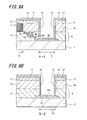
- FIG. 10A the shield film 18 placed on the upper portions of the effective pixel region 3a and the pad portion 5 (see FIG. 2 ) is removed using a resist mask.
- the shield film 18 is selectively deposited on the internal side-wall of the opening 16 excluding the portions of photodiodes 11 (light-receiving portion) in the effective pixel region 3a and the pad portion 5 shown in FIG. 2 .
- the shield film 18 is not deposited on the opening 16 of the pad portion 5 but is deposited on the optical black region
- the shield film 18 is deposited on the internal side-wall and the bottom of the opening 16 of the ground connecting pad portion 5g.
- the shield film 18 is connected to the ground interconnect 15 at the bottom of the opening 16 of the ground connecting pad portion 5g.
- the potential of the shield film 18 formed is fixed to the same potential as the ground potential.
- the opening 16 is formed in the preceding step to the step of depositing the silicon oxide film 17. Since one of the openings 16 is formed as the ground connecting pad portion 5g that exposes the ground interconnect and the shield film 18 is deposited on the internal side-wall and the bottom of the opening 16 of the ground connecting pad portion 5g in the step of depositing the shield film 18, the potential of the shield film 18 is fixed to the same potential as the ground potential. Since the silicon oxide film 17 is deposited on the internal side-wall of the opening 16, the shield film 18 will not directly be in contact with the Si semiconductor 10 and the plurality of wiring layers 9.
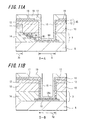
- the passivation film 19 for planarization is deposited thereon as illustrated in FIGS. 11A, 11B .
- the passivation film is deposited on the entire surface including the internal side-wall and the bottom of the opening 16.
- a silicon nitride (SiN) film can be used, and a plasma nitride film can more preferably be used.
- first resist layers 20 are placed in the openings 16 that form the pad portion 5 and the ground connecting pad portion 5g.
- on-chip color filters CF are formed corresponding to the photodiodes 11 in the effective pixel region 3a and the optical black region 3b (see FIG. 2 .).
- the on-chip color filters CF each corresponding to one of the colors R (red), G (green), B (blue) are formed so as to match with positions of the respective photodiodes 11.
- the on-chip color filters CF are formed by applying a resist for each color, exposing the resist, and developing the resist. Since the effective pixel region 3a and the optical black region 3b are not shown in the cross sectional configuration in FIG. 13B , the on-chip color filters CF are not illustrated in FIG. 13B .
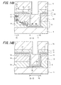
- the on-chip microlens film 21 is applied on the entire surface of the passivation film 19 including the surfaces of the on-chip color filters CF.
- the on-chip microlens film 21 is an organic material, an example of which includes novolac resin. The material is fabricated as an on-chip microlens in the subsequent step.
- a second resist layer 26 is formed on positions corresponding to each of the on-chip color filters CF, and the second resist layer is then exposed, developed, reflowed to form a structure of the on-chip microlens.
- the entire surface of the second resist layer 26 is etched.
- a shape of the on-chip microlens film 21 is transformed into the shape of the second resist layer 26 shown in FIG. 15A to form the on-chip microlenses 25 in the effective pixel region 3a and the optical black region 3b.
- the first resist layer 20 placed in the openings 16 of the pad portion 5 and the ground connecting pad portion 5g is removed, thereby forming the openings 16 again.
- the first resist layer 20 placed in the openings 16 is etched so as to expose the interconnect M4 as shown in FIG.
- the shield film 18 is exposed in the example shown in FIG. 16B ; however, since the ground interconnect 15 has been in contact with the shield film 18, small amounts of the passivation film 19 or other films can be remained on the shield film 18. Further, as shown in FIG. 16B , since the passivation film 19, the on-chip maicrolens film 21, and the first resist layer 20 are formed in this order on the shield film 18 on the internal side-wall of the opening 16, moisture resistance of the shield film 18 on the internal side-wall can be improved, thereby preventing deterioration of the shield film 18.
- the bonding wires 24 are wire-bonded with the interconnect M4 exposed from the bottom of the opening 16, thereby taking out the electrode to the outside.
- Au fine wires may be employed as the bonding wires 24.
- the potential of the shield film 18 is fixed to the same potential as the ground potential.
- a method of fabricating a solid-state imaging device includes forming the opening 16 including the pad portion 5 and the ground connecting pad portion 5g prior to depositing the insulating film and the silicon oxide film 17, both forming the antireflective film 45.
- the silicon oxide film 17 forming part of the antireflective film 45 can be uniformly formed on the internal side-wall of the opening 16.
- the shield film 18 and the bonding wires 24 will not be in contact with the Si semiconductor layer 10 in a case where the shield film 18 and the bonding wires 24 are formed on the internal side-wall of the opening 16.
- the step of connecting the shield film 18 to ground can simultaneously be carried out with the step of depositing the shield film 18. Since the shield film 18 on the internal side-wall of the opening 16 of the ground connecting pad portion 5g is covered with the passivation film 19 and on-chip microlens film 21, the moisture resistance of the shield film 18 can be improved, thereby preventing deterioration of the shield film 18.
- tungsten is used as a material of the shield film 18; however, other materials such as aluminum (Al), molybdenum (Mo), ruthenium (Ru), and iridium (Ir) may also be used.
- Al aluminum
- Mo molybdenum
- Ru ruthenium
- Ir iridium
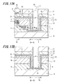
- FIG. 17 is a schematic diagram illustrating a solid-state imaging device according to a second embodiment of the invention.
- the solid-state imaging device according to this embodiment aluminum is used as a material of the shield film, and the same reference numerals as those used in FIGS. 4, 5 are used to denote the corresponding parts in FIGS. 17A, 17B , and duplicated descriptions thereof are thus omitted.
- the solid-state imaging device according to the second embodiment includes the same configuration as that shown in FIG. 1 .
- FIG. 17A shows the A-A cross-sectional configuration while FIG. 17B shows the B-B cross-sectional configuration in FIG. 2 .
- the solid-state imaging device according to the second embodiment is manufactured in compliance with the fabricating steps for the first embodiment; however, the location of depositing a shield film 22 in the second embodiment is different from that shown in the first embodiment.
- an area of the shield film 22 corresponding to the effective pixel region 3a is etched in the similar manner as the first embodiment; however, an area of the shield film 22 corresponding to the opening 16 of the pad portion 5 is not etched.
- the shield film 22 is partially removed to form an insulating portion 23 such that the areas of the shield film 22 corresponding to the opening portion 16 of the pad portion 5 is electrically insulated from other areas of the shield film 22 including those corresponding to the opening portion of the ground connecting pad portion 5g.
- the areas of the shield film 22 corresponding to the opening portion 16 of the pad portion 5 is electrically cut off from other areas of the shield film 22 formed on the ground connecting pad portion 5g by forming the insulating portion 23 in the shield film.
- the area of the shield film 22 corresponding to the opening 16 of the pad portion 5 is electrically insulated from the area of the shield film 22 corresponding to the ground connecting pad portion 5g.
- the passivation filrm 19, on-chip color filters CF, and on-chip microlenses 25 are formed in the similar steps as those conducted in the first embodiment.
- the bottom of the opening 16 of the pad portion 5 is etched so as to expose the shield film 16 as shown in FIG. 17A .
- the bottom of the opening 16 of the ground connecting pad portion 5g is etched so as not to etch the shield film 22.
- the shield film 22 is exposed in the example shown in FIGS. 17A, 17B ; however, since the interconnect has been in contact with the shield film 22, small amounts of the passivation film 19 or other films can be remained on the shield film 22.
- the shield film 22 made of aluminum (Al) is brought into contact with the ground connecting interconnect 15 exposed from the opening 16 in the ground connecting pad portion 5g, the potential in the area of the shield film 22 corresponding to the ground connecting pad portion 5g is fixed to the same potential as the ground potential.
- the bonding wire 24 made of gold (Au) is connected to the external electrode and the interconnect M4 via the shield film 22 in the opening 16 of the pad portion 5.
- the shield film 22 made of aluminum (Al) is alloyed with the boding wire 24 made of Au.
- the internal side-wall of the opening 16 corresponding to the pad portion 5 in this embodiment is coated with the shield film 22 formed of metal layers via the insulating film formed of the silicon oxide film 17. Since one metal layer (shield film 22) is formed on the internal side-wall of the opening 16 of the pad portion 5 in this manner, it is possible to reduce damage to the insulating film (silicon oxide film 17) formed on the internal side-wall of the opening 16 of the pad portion 5 in wire bonding. Further, the leak current can be prevented from flowing between the bonding wire 24 made of gold (Au) and the silicon layer 10 forming a semiconductor layer.
- the interlayer dielectric 14 of the plurality of wiring layers 9 can be prevented from being exposed from the opening 16, and absorption of moisture in the metal interconnects used in the plurality of wiring layers 9 and in the interlayer dielectric 14 can also be prevented. Further, the passivation capability of the insulating film (silicon oxide film 17) can be increased by forming the metal layer (shield film 22) on the internal side-wall of the opening 16 of the pad portion 5.
- a camera may be formed with the solid-state imaging device 1 of the aforementioned first or second embodiment.
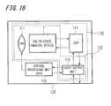
- FIG. 18 shows a camera including the solid-state imaging device of the embodiment.
- the camera 110 shown in FIG. 18 is configured to include the backside-illuminated imaging device 1, an optical lens system 111, an input-output unit 112, a signal processor 113, and a central processing unit for controlling the optical lens system as one assembly.
- the backside-illuminated imaging device 1 can be configured to include the optical lens system 111, the input-output unit 112, and the signal processor 113.
- a camera 115 is configured to only include the solid-state imaging device 1, the optical lens system 111, and the input-output unit 112.
- a camera 116 is configured to include the solid-state imaging device 1, the optical lens system 111, the input-output unit 112, and the signal processor 113.
Landscapes
- Solid State Image Pick-Up Elements (AREA)
- Transforming Light Signals Into Electric Signals (AREA)
Abstract
Description
- The present invention contains subject matter related to Japanese Patent Application
JP 2008-010904 - The invention relates to a backside-illuminated solid-state imaging device, a method of fabricating the backside-illuminated solid-state imaging device, and a camera.
- In a CMOS type solid-state imaging device, there has been disclosed a backside-illuminated solid-state imaging device for improving photoelectric conversion efficiency and sensitivity to incident light. In the backside-illuminated solid-state imaging device, light is illuminated from backside of the solid-state imaging device. The backside-illuminated solid-state imaging device is configured to include a semiconductor substrate on which photodiodes as photoelectric converters, pixel transistors, a plurality of wiring layers forming a signal circuitry, and the like are formed (see Japanese Unexamined Patent Application Publication No.
2005-347707 2005-353631 - The backside-illuminated solid-state imaging device includes a pad portion formed on a rear side of the semiconductor substrate that can supply predetermined electrical potential to a multilayer interconnect formed on a front-surface side of the semiconductor substrate.
-
FIG. 1 is a schematic cross-sectional configuration diagram illustrating a backside-illuminated solid-state imaging device according to the related art. The cross-sectional configuration diagram inFIG. 1 specifically illustrates a region that includes apad portion 60 formed in a peripheral region of a rear side of the backside-illuminated solid-state imaging device. - The backside-illuminated solid-
state imaging device 70 includes an imaging region in whichphotodiodes 54 each used as a photoelectric converter and a plurality of pixels including pixel transistors (MOS transistors), a peripheral circuitry are formed on asemiconductor Si layer 53, and apad portion 60 formed in a peripheral region of a rear side thereof. Although not shown in the figure, the pixel transistors each forming a pixel are formed on a front-surface side of theSi layer 53. Further, multi-layer interconnects 52 (e.g., Cu interconnects) and a plurality ofwiring layers 51 including a wire-bondingAL interconnect 52a are formed on a surface of theSi layer 53 via an interlayer dielectric 61. A supportingsubstrate 50 formed of a silicon substrate is formed on a front-surface side of the plurality ofwiring layers 51. - In contrast, an
insulating film 55 used as an antireflective film, ashield film 56, and apassivation film 57 are multiply layered in this order on a rear side of theSi layer 53. Further, on-chip color filters are formed on thepassivation film 57 corresponding to the imaging region, and on-chip microlenses 53 are formed on thepassivation film 57. The imaging region includes an optical black region formed outside of an effective pixel region for specifying black levels of images. Pixels and color filters similar to the pixels in the effective pixel region are formed in the optical black region. Theshield film 56 is formed over an entire surface including other pixel transistors and peripheral circuitries except for light-receiving portions in the effective pixel region, namely, thephotodiodes 54 andpad portions 60. - The
pad portion 60 includes anopening 62 to expose theAL interconnect 52a connected topredetermined interconnects 52 of the plurality ofwiring layers 51. Specifically, after the on-microchiplenses have been formed, anopening 62 is formed such that desiredAl interconnects 52a are exposed from a rear surface of the backside-illuminated solid-state imaging device 70 towards a front-surface thereof on which themultilayer interconnection layer 51 is formed, thereby forming thepad portion 60 for taking out an electrode. In this process, thepad portion 60 is formed by etching theSi layer 53 includingphotodiodes 54 formed thereon, aninsulating film 55 formed on an incident light surface of theSi layer 53, an interlayer dielectric 61 of the plurality ofwiring layers 51, and the like. In thepad portion 60 formed in this manner, for example, Au fine wires (so called bonding wires) 63 are connected toAl interconnects 52a (wire-bonding) that are exposed from theopening 62. - However, in the related art backside-illuminated solid-state imaging devices, since the
Si layer 53 is exposed from an internal sidewall of thepad portion 60, theSi layer 53 and the Aufine wires 63 are brought into contact when the Aufine wires 63 are wire-bonded to the Al interconnects 52a in thepad portion 60. Therefore, current is likely to flow between a well region (e.g., p-type well region) for the Aufine wires 63 having ground potential and a region having different potential. That is, leak current flows from the Aufine wires 63 to theSi layer 53. - The interlayer dielectric 61 of the plurality of
wiring layers 51 is exposed from the internal sidewall of theopening 62 forming thepad portion 60. The interlayer dielectric 61 includes metal used as theinterconnects 52 forming a signal circuitry. Thus, only providing the interlayer dielectric 61 that is exposed from the opening 62 may not be sufficient to prevent theinterconnects 52 from absorbing moisture. That is, S09P0033 theinterconnects 52 may deteriorate under a high-humidity environment. In the cutting-edge CMOS process, an insulating film with a small dielectric constant (a Low-κ dielectric) is used as the interlayer dielectric 61 of the plurality ofwiring layers 51; however, a film property of the Low-κ dielectric may also deteriorate under such high-humidity environment, thereby exhibiting no moisture resistance in the interlayer dielectric 61. - Japanese Unexamined Patent Application Publication No.
2005-347707 - Further, since the related art shield film used in the backside-illuminated solid-state imaging device is electrically floating, electrical potential is not stabilized. As a result, the electrical potential of the shield film may cause an adverse effect on pixels of the solid-state imaging device.
- Embodiments of the invention intend to provide a solid-state imaging device that exhibits excellent reliability, a method of fabricating the solid-state imaging device, and a camera.
- An embodiment of the invention intends to provide a solid-state imaging device receiving incident light from a backside thereof. The imaging device includes a semiconductor layer on which a plurality of pixels including photoelectric converters and pixel transistors are formed, a plurality of wiring layers formed on a first surface of the semiconductor layer, a pad portion formed on a second surface of the semiconductor layer, an opening formed to reach a conductive layer of the plurality of wiring layers, and an insulating film extendedly coated from the second surface to an internal side-wall of the opening so as to insulate the semiconductor layer.
- An embodiment of the invention also provides a method of fabricating a solid-state imaging device. The method includes forming a plurality of wiring layers on a first surface of a semiconductor layer on which a plurality of pixels including photoelectric converters and pixel transistors, forming an opening corresponding to a pad portion of a second surface of the semiconductor layer to reach a conductive layer of the plurality of wiring layers, and forming an insulating film extendedly coated from the second surface to an internal side-wall of the opening so as to insulate the semiconductor layer.
- An embodiment of the invention further provides a camera including a solid-state imaging device, an optical lens, and a signal processor. In the camera, the solid-state imaging device includes a semiconductor layer on which a plurality of pixels including photoelectric converters and pixel transistors are formed, a plurality of wiring layers formed on a first surface of the semiconductor layer, a pad portion formed on a second surface of the semiconductor layer, an opening formed to reach a conductive layer of the plurality of wiring layers, and an insulating film extendedly formed from the second surface to an internal side-wall of the opening so as to coat the semiconductor layer.
- In an embodiment of the invention, the insulating film is extendedly formed from the surface of the semiconductor layer to the internal side-wall of the opening of the pad portion formed on the solid state imaging device to insulate the semiconductor layer, advert effect on the semiconductor layer and the plurality of wiring layers may be prevented.
- According to an embodiment of the invention, since the insulating film is extendedly coated from the surface of the semiconductor layer to the internal side-wall of the opening of the pad portion, the advert effect on the semiconductor layer and the plurality of wiring layers may be prevented, thereby improving product reliability of the solid-state imaging device.
-
-
FIG. 1 is a schematic cross-section configuration diagram illustrating a solid-state imaging device according to the related art. -
FIG. 2 is a schematic diagram illustrating a solid-state imaging device according to a first embodiment of the invention. -
FIG. 3 is a schematic cross-sectional configuration diagram illustrating main parts of the solid-state imaging device according to the embodiment of the invention. -
FIG. 4 is a schematic cross-section configuration diagram illustrating a pad portion used in the solid-state imaging device according to the embodiment of the invention. -
FIG. 5 is a schematic cross-sectional configuration diagram illustrating a ground connection pad portion used in the solid-state imaging device according to the embodiment of the invention. -
FIGS. 6A, 6B are respectively a cross-section configuration diagram along the line A-A, and a cross-sectional configuration diagram along the line B-B (part one) of the solid-state imaging device according to the embodiment of the invention. -
FIGS. 7A, 7B are respectively a cross-section configuration diagram along the line A-A, and a cross-sectional configuration diagram along the line B-B (part two) of the solid-state imaging device according to the embodiment of the invention. -
FIGS. 8A, 8B are respectively a cross-section configuration diagram along the line A-A, and a cross-sectional configuration diagram along the line B-B (part three) of the solid-state imaging device according to the embodiment of the invention. -
FIGS. 9A, 9B are respectively a cross-section configuration diagram along the line A-A, and a cross-sectional configuration diagram along the line B-B (part four) of the solid-state imaging device according to the embodiment of the invention. -
FIGS. 10A, 10B are respectively a cross-section configuration diagram along the line A-A, and a cross-sectional configuration diagram along the line B-B (part five) of the solid-state imaging device according to the embodiment of the invention. -
FIGS. 11A, 11B are respectively a cross-section configuration diagram along the line A-A, and a cross-sectional configuration diagram along the line B-B (part six) of the solid-state imaging device according to the embodiment of the invention. -
FIGS. 12A, 12B are respectively a cross-section configuration diagram along the line A-A, and a cross-sectional configuration diagram along the line B-B (part seven) of the solid-state imaging device according to the embodiment of the invention. -
FIGS. 13A, 13B are respectively a cross-section configuration diagram along the line A-A, and a cross-sectional configuration diagram along the line B-B (part eight) of the solid-state imaging device according to the embodiment of the invention. -
FIGS. 14A, 14B are respectively a cross-section configuration diagram along the line A-A, and a cross-sectional configuration diagram along the line B-B (part nine) of the solid-state imaging device according to the embodiment of the invention. -
FIGS. 15A, 15B are respectively a cross-section configuration diagram along the line A-A, and a cross-sectional configuration diagram along the line B-B (part 10) of the solid-state imaging device according to the embodiment of the invention. -
FIGS. 16A, 16B are respectively a cross-section configuration diagram along the line A-A, and a cross-sectional configuration diagram along the line B-B (part 11) of the solid-state imaging device according to the embodiment of the invention. -
FIGS. 17A, 17B are respectively a cross-section configuration diagram along the line A-A, and a cross-sectional configuration diagram along the line B-B of a solid-state imaging device according to a second embodiment of the invention. -
FIG. 18 is a schematic diagram illustrating a camera according to an embodiment of the invention. - Embodiments of the invention will be described below with reference to accompanying drawings.
-
FIG. 2 is a schematic diagram illustrating a solid-state imaging device according to a first embodiment of the invention. A solid-state imaging device according to embodiments of the invention is a backside-illuminated CMOS solid-state imaging device. - A solid-state imaging device according to an embodiment of the invention is configured to include
imaging region 3,peripheral circuitries pad portions 5. - The
imaging region 3 includes a matrix of numerous unit pixels, and address lines arranged in rows, and signal lines arranged in columns. Theimaging region 3 includes aneffective pixel region 3a and an opticalblack region 3b that determines a black level of each pixel. - The optical
black region 3b also includes similar pixels as those included in theeffective pixel region 3a. The pixels in the opticalblack region 3b are arranged outside of theeffective pixel region 3a. An entire region of the solid-state imaging device, excluding the photoelectric converters (light-receiving portion) of theeffective pixel region 3a and thepad portions 5, is covered with the shield film. - Each pixel in the
imaging region 3 includes the photoelectric converter such as a photodiode and a plurality of pixel transistors (MOS transistors). Each of the pixel transistors may include four transistors, examples of which include a transferring transistor, a resetting transistor, an amplifying transistor, and a selecting transistor. Alternatively, each pixel transistor may simply include three transistors, examples of which include the transferring transistor, the resetting transistor, and the amplifying transistor. Or, each pixel transistor may include other transistors. -
FIG. 3 shows an example of a cross sectional structure of the unit pixel. In this example, a unit pixel 31a is formed by forming a second conductive p-typepixel separating region 32, a photodiode (PD) 11 as a photoelectric converter and a plurality of pixel transistors Tr1, Tr2 on a first conductive n-typesilicon semiconductor layer 10. Thephotodiode 11 includes an n-type semiconductor layer 10 surrounded by a p-typepixel separating region 32 and a relatively deeply formed p-typesemiconductor well region 35 in which the pixel transistors Tr1 and Tr2 are formed, and p+ accumulation layers 33, 34 for controlling dark current on both front-surface and rear-surface sides of the solid-state imaging device. The n-type semiconductor layer 10 forming thephotodiode 11 includes a highly concentrated n+ charge-storingregion 10a and a lowly concentrated n-type region 10b forming the n-type semiconductor layer 10. The n-type region 10b of the n-type semiconductor 10 is extendedly formed below the p-typesemiconductor well region 35 in which the pixel transistors Tr1, Tr2 are formed. - The pixel transistors Tr1, Tr2, for example, each include four transistors as described earlier. In the figure, Tr1 indicates a transferring transistor, and Tr2 indicates other transistors such as a resetting transistor, an amplifying transistor, or a selecting transistor. The pixel transistor Tr1 includes the n+ source-
drain region 37 of floating diffusion, the n+ charge-storingregion 10a of thephotodiode 11, and agate electrode 41 formed via a gate insulating film. The pixel transistor Tr2 includes a pairedsource drain regions gate electrode 42. - A plurality of
wiring layers 9 having interconnects M1 to M4 multiply layered via aninterlayer dielectric 14 is formed on a front-surface of thesemiconductor layer 10, and a supportingsubstrate 8 formed such as a silicon substrate is bonded to the plurality of wiring layers 9. The interconnects M1 to M3 in the first to third layers forms a signal circuitry which is formed of Cu interconnects by damascene process. The interconnect M4 in the fourth layer is a conductive layer including Al interconnects that is connected with Au fine wires wire-bonding process. - An insulating film used as
antireflective film 45 is provided with a rear side of thesemiconductor layer 10. Theantireflective film 45 is formed of a film stack having a nitride film (SiN) 12 and a silicon oxide (SiO2)film 17 stacked on thesemiconductor layer 10 in this order. Theshield film 18 is formed on theantireflective film 45 excluding a light-receiving portion for a photodiode, and apassivation film 19 is further formed over theshield film 18. Thepassivation film 19 may be formed of a planarized film. Theshield film 18 is formed of a metal film. Further, an on-chip color filters CF for primary colors of red (R), green (G), blue (B) are formed on thepassivation film 19 corresponding to the imaging region, and on-chip microlenses 25 are formed on the on-chip color filters CF. - In contrast, although not shown in the figure,
peripheral circuitries imaging region 3 in a vertical direction, and then supplies to the column signal processing circuitry signal charge generated based on an amount of light received by the photoelectric converter for each pixel via vertical signal lines. The column signal processing circuitries are arranged for each column of the pixels, and signals output by the pixels per row is signal-processed per pixel column such as noise cancellation or signal amplification with signals output by the black reference pixels in the optical black region. A horizontal selecting switch is connected between horizontal signal lines in an output stage of the column signal processing circuitry. The horizontal driving circuitry may be formed of a shift register that sequentially selects pixels per column of the column signal circuitry by sequentially outputting horizontal pulses, and then causes each of the column signal processing circuitries to output the pixel signals to the horizontal signal lines. The output circuitry signal processes the signals sequentially supplied from each of the column signal processing circuitries via the horizontal signal lines, and outputs the resulting signals. - Since the solid-
state imaging device 1 of the embodiment is backside-illuminated type, a plurality ofpad portions 5 are formed around the imaging region thereof such that interconnects formed on the front-surface of the solid-state imaging device 1 can be taken out of thepad portions 5. One of thepad portions 5 is used as a ground interconnect (hereinafter called "ground connecting pad portion") 5g. In the ground connectingpad portion 5g, a ground interconnect is connected with theshield film 18 as will be described later. The ground connectingpad portion 5g includes an opening formed in the same step as the step of forming an opening in thepad portion 5. -
FIG. 4 illustrates a cross sectional structure of thepad portion 5 along A-A line inFIG. 2 . According to the solid-state imaging device 1 of the embodiment, insulation is securely formed so as to separate bonding wires, such as Au fine wires wire-bonded with thepad portions 5, from thesemiconductor layer 10 in thepad portion 5 as shown inFIG. 4. FIG. 5 illustrates a cross sectional structure of the ground connectingpad portion 5g along B-B line inFIG. 2 . As shown inFIG. 5 , in the ground connectingpad portion 5g, ground potential is provided with theshield film 18, and insulation is securely formed to separate theshield film 18 with the ground potential from thesemiconductor layer 10. - As shown in
FIG. 4 , adequate Cu interconnects of M1, M2, and M3 are connected in the plurality of wiring layers 9. In this embodiment, the interconnects M1 to M3 are connected, and interconnects M3 and M4 (conductive layer) are connected. The interconnect M4 is extended to a portion corresponding to thepad portion 5. Thepad portion 5 includes anopening 16 such that the Al interconnect M4 is exposed from the surface of the on-chip microlens film 21, on which the on-chip microlenses 25 are formed. Asilicon oxide film 17,passivation film 19, and on-chip microlens film 21 that form an antireflective film are provided as an insulating film on an internal side-wall of theopening 16 so as to cover thesemiconductor layer 10. The Al interconnect M4 is exposed from a bottom of theopening 16. Theshield film 18 is not formed on a region corresponding to theopening 16. - Bonding wires such as Au
fine wires 24 are wire-bonded with the Al interconnect M4 exposed from the bottom face of thepad portion 5. In thepad portion 5, an insulating film including thesilicon oxide film 17,passivation film 19, and on-chip microlens film 21 are extendedly formed such that thesemiconductor layer 10 on the internal side-wall of theopening 16 is insulated, thereby preventing contingent current leak. The interconnects M1 to M4 of the plurality ofwiring layers 9 and theinterlayer dielectric 14 can be prevented from absorbing moisture. Thus, the reliability of the solid-state imaging device can be improved. - As shown in
FIG. 5 , of the interconnects M1 to M4 (not shown in the figure) in the plurality ofwiring layers 9, the ground interconnect (conductive layer) 15 connected to the predetermined interconnects to which ground potential is supplied is extended to a position corresponding to a position of the ground interconnectingpad portion 5g. Theground interconnect 15 is formed of Al fine wires, and formed simultaneously with the interconnect M4 in the same layer thereof. The groundinterconnecting pad portion 5g includes theopening 16 formed from the surface of the on-chip microlens film 21 to theground interconnect 16, thesilicon oxide film 17 used as an antireflective film in the imaging region on the internal side-wall of theopening 16 so as to insulate thesemiconductor layer 10, and anextended portion 18a of theshield film 18 formed from internal side-wall of theopening 16 to the bottom thereof so that theshield film 18 is electrically connected to theground interconnect 15. Further, thepassivation film 19 and themicrolens film 21 are also extendedly formed on the internal side-wall of theopening 16. Although not shown in the figure, theground interconnect 15 is electrically connected to thepad portion 5 to which the ground potential is supplied. A configuration of thepad portion 5 to which the ground potential is supplied is substantially the same as that of thepad portion 5 inFIG. 4 . - In the ground connecting
pad portion 5g having such a configuration, since theextended portion 18a of theshield film 18 is electrically connected to theground interconnect 15 extended to theopening 16, theshield film 18 is set to the ground potential and is electrically stabilized. Further, since thesilicon oxide film 17 forming the antireflective film and extendedly formed on the internal side-wall of the opening provides insulation between thesemiconductor layer 10 andshield film 18, thesemiconductor layer 10 is securely insulated from theshield film 18. Since thepassivation film 19 and on-chip microlens film 21 are extendedly formed on the internal side-wall of theopening 16, absorption of moisture in the interconnects M1 to M4 in the plurality ofwiring layers 9 can be prevented. Thus, the reliability of the solid-state imaging device can be improved. - Next, a method of fabricating the aforementioned solid-
state imaging device 1, in particular, a method of fabricating the pad portion having a cross sectional configuration along A-A and B-B inFIG. 2 is described with reference toFIGS. 6A, 6B to 17 . The A-A cross sectional configuration indicates a cross sectional configuration of thepad portion 5 and the opticalblack region 3b whereas the B-B cross sectional configuration indicates a cross sectional configuration of the ground connectingpad portion 5g of the shield film. - First, as shown in
FIGS. 6A, 6B , there is provided a structure including theSi semiconductor layer 10, the plurality ofwiring layers 9 formed on the front-surface of theSi semiconductor layer 10, and the supportingsubstrate 8 provided on the front-surface of the plurality of wiring layers 9. The imaging region of theSi semiconductor layer 10 includes two dimensionally arranged pixels formed ofphotodiodes 11 each used as a photoelectric converter and a plurality of pixel transistors.
A method of fabricating the structure includes forming thesemiconductor layer 10 and the plurality ofwiring layers 9 on a separate substrate; bonding the supportingsubstrate 8 on a surface of the plurality ofwiring layers 9; and removing the substrate on which thesemiconductor layer 10 has been formed. - In the plurality of
wiring layers 9, a plurality of interconnects including those for signal circuitries and other components are formed via theinterlayer dielectric 14, for a material of which silicon oxide film (SiO2) is used.FIG. 6A is one example of the plurality ofwiring layers 9 including four interconnects M1, M2, M3, M4, each of which is connected to one of predetermined interconnects via acontact hall 13. In this embodiment, the interconnect M4 is wire-bonded to an external connection in the later-describedpad portion 5. The interconnect M4 is made of Aluminum (A1) so as to have an excellent connection with Au bonding wire. The first to third interconnects M1 to M3 can be made either of A1 or Cu. If the interconnects M1 to M3 are made of Cu, the interconnects M1 to M3 will exhibit excellent conductivity. The plurality ofwiring layers 9 inFIG. 6B also includes predetermined interconnects; however, only theground interconnect 15 is illustrated inFIG. 6B . Theground interconnect 15 is placed so as to brought into contact with the shield film in the later-described ground connectingpad portion 5g, thereby setting potential of the shield film to be congruent with the ground potential.
Since the cross sectional configuration along the line B-B of the solid-state imaging device 1 inFIG. 2 excludes theeffective pixel region 3a and the opticalblack region 3b, thephotodiodes 11 are not formed on theSi semiconductor layer 10. - Referring back to
FIG. 6B , a nitride film (SiN) 12 forming theantireflective film 45 is formed on the entire surface of theSi semiconductor layer 10. In this embodiment, the nitride film is used as theantireflective film 45; however, theantireflective film 45 may be configured to include the nitride film and a hafnium oxide (HfO2) film stacked thereon.
In this embodiment, the front-surface of the solid-state imaging device is defined as a side forming the plurality ofwiring layers 9 whereas the rear-surface thereof is defined as a side forming the antireflective film, in viewing from theSi semiconductor layer 10 on which thephotodiodes 11 are formed. - Next, as illustrated in
FIGS. 7A, 7B , theopenings 16 are formed by etching portions of the structure corresponding to thepad portion 5 and the ground connectingpad portion 5g. InFIG. 7A , theopening 16 is formed so as to expose the interconnect M4, whereas inFIG. 7B , theopening 16 is formed so as to expose theground interconnect 15. - Next, as illustrated in
FIGS. 8A, 8B , the silicon oxide (SiO2)film 17 is deposited on the surface of thenitride film 12. The silicon oxide film is deposited on a sidewall and a bottom of theopening 16. In this embodiment, theantireflective film 45 is formed of a two-layered film including thenitride film 12 and the silicon oxide film. - As illustrated in
FIGS. 9A, 9B , thesilicon oxide film 17 formed on the bottom of theopening 16 is selectively removed by etching. For example, after portions other than the bottom of theopening 16 have been masked with a resist film, thesilicon oxide film 17 can be removed by dry-etching. The interconnect M4 and theground interconnect 15 are re-exposed from the bottom of theopening 16 in this manner. After having selectively removed thesilicon oxide film 17, theshield film 18 is deposited on the entire internal side-wall of theopening 16. As examples of a material for theshield film 18 having shielding properties, tungsten (W), aluminum (Al), molybdenum (Mo), iridium (Ir) can be given. Theshield film 18 is deposited on the entire internal side-wall of theopening 16 by sputtering process or CVD process. A shield film deposited by sputtering process can exhibit more adhesiveness than a shield film made by CVD process. When the shield film is deposited by sputtering, the grain size of the material is relatively large; however, the grain size of the material is relatively small by CVD process, thereby improving the shielding properties of the material deposited by CVD process in comparison to that deposited by sputtering. Alternatively, the shield film may be deposited by sputtering and CVD processed in combination. In this embodiment, tungsten (W) is used as a material for theshield film 18. - Subsequently, as illustrated in
FIGS 10A, 10B , theshield film 18 placed on the upper portions of theeffective pixel region 3a and the pad portion 5 (seeFIG. 2 ) is removed using a resist mask. Theshield film 18 is selectively deposited on the internal side-wall of theopening 16 excluding the portions of photodiodes 11 (light-receiving portion) in theeffective pixel region 3a and thepad portion 5 shown inFIG. 2 .
For example, as illustrated inFIG. 10A , theshield film 18 is not deposited on theopening 16 of thepad portion 5 but is deposited on the opticalblack region 3b. As illustrated inFIG. 10B , theshield film 18 is deposited on the internal side-wall and the bottom of theopening 16 of the ground connectingpad portion 5g. Theshield film 18 is connected to theground interconnect 15 at the bottom of theopening 16 of the ground connectingpad portion 5g. Thus, the potential of theshield film 18 formed is fixed to the same potential as the ground potential. In this embodiment, theopening 16 is formed in the preceding step to the step of depositing thesilicon oxide film 17. Since one of theopenings 16 is formed as the ground connectingpad portion 5g that exposes the ground interconnect and theshield film 18 is deposited on the internal side-wall and the bottom of theopening 16 of the ground connectingpad portion 5g in the step of depositing theshield film 18, the potential of theshield film 18 is fixed to the same potential as the ground potential. Since thesilicon oxide film 17 is deposited on the internal side-wall of theopening 16, theshield film 18 will not directly be in contact with theSi semiconductor 10 and the plurality of wiring layers 9. - After the
shield film 18 has been formed on the predetermined position, thepassivation film 19 for planarization is deposited thereon as illustrated inFIGS. 11A, 11B . The passivation film is deposited on the entire surface including the internal side-wall and the bottom of theopening 16. As thepassivation film 19, a silicon nitride (SiN) film can be used, and a plasma nitride film can more preferably be used. - Next, as illustrated in
FIGS. 12A, 12B , first resistlayers 20 are placed in theopenings 16 that form thepad portion 5 and the ground connectingpad portion 5g. - As illustrated in
FIGS. 13A, 13B , on-chip color filters CF are formed corresponding to thephotodiodes 11 in theeffective pixel region 3a and the opticalblack region 3b (seeFIG. 2 .). In this embodiment, the on-chip color filters CF each corresponding to one of the colors R (red), G (green), B (blue) are formed so as to match with positions of therespective photodiodes 11. The on-chip color filters CF are formed by applying a resist for each color, exposing the resist, and developing the resist. Since theeffective pixel region 3a and the opticalblack region 3b are not shown in the cross sectional configuration inFIG. 13B , the on-chip color filters CF are not illustrated inFIG. 13B . - As shown in
FIGS. 14A, 14B , the on-chip microlens film 21 is applied on the entire surface of thepassivation film 19 including the surfaces of the on-chip color filters CF. The on-chip microlens film 21 is an organic material, an example of which includes novolac resin. The material is fabricated as an on-chip microlens in the subsequent step. - Next, as shown in
FIG. 15A , having applied the on-chip microlens film 21, a second resistlayer 26 is formed on positions corresponding to each of the on-chip color filters CF, and the second resist layer is then exposed, developed, reflowed to form a structure of the on-chip microlens. - Finally, as shown in
FIGS 16A, 16B , the entire surface of the second resistlayer 26 is etched. As illustrated inFIG. 16A , a shape of the on-chip microlens film 21 is transformed into the shape of the second resistlayer 26 shown inFIG. 15A to form the on-chip microlenses 25 in theeffective pixel region 3a and the opticalblack region 3b. Further, with the etching process, the first resistlayer 20 placed in theopenings 16 of thepad portion 5 and the ground connectingpad portion 5g is removed, thereby forming theopenings 16 again. The first resistlayer 20 placed in theopenings 16 is etched so as to expose the interconnect M4 as shown inFIG. 16A whereas the first resistlayer 20 is etched so as not to etch theshield film 18 as shown inFIG. 16B . Theshield film 18 is exposed in the example shown inFIG. 16B ; however, since theground interconnect 15 has been in contact with theshield film 18, small amounts of thepassivation film 19 or other films can be remained on theshield film 18. Further, as shown inFIG. 16B , since thepassivation film 19, the on-chip maicrolens film 21, and the first resistlayer 20 are formed in this order on theshield film 18 on the internal side-wall of theopening 16, moisture resistance of theshield film 18 on the internal side-wall can be improved, thereby preventing deterioration of theshield film 18. - In the
pad portion 5 formed in this manner, thebonding wires 24 are wire-bonded with the interconnect M4 exposed from the bottom of theopening 16, thereby taking out the electrode to the outside. In this embodiment, Au fine wires may be employed as thebonding wires 24. - In this embodiment, since a layer including the
silicon oxide film 17, thepassivation film 19, and the on-chip microlens film 21 is formed on the internal side-wall of theopening 16, current will not be leaked from thebonding wires 24 via theSi semiconductor layer 10 due to the difference in the potential between the areas in theSi semiconductor layer 10. Moreover, since exposure of theinterlayer dielectric 14 of the plurality ofwiring layers 9 from the internal side-wall of theopening 16 can be prevented, absorption of moisture can be prevented in the interconnects included in the plurality ofwiring layers 9 and theinterlayer dielectric 14. Thus, the product reliability of the solid-state imaging device increases with an increase of the moisture resistance of the plurality of wiring layers 9. - Further, in this embodiment; since the
shield film 18 is connected with theground interconnect 15 in the ground connectingpad portion 5g, the potential of theshield film 18 is fixed to the same potential as the ground potential. - In this embodiment, a method of fabricating a solid-state imaging device includes forming the
opening 16 including thepad portion 5 and the ground connectingpad portion 5g prior to depositing the insulating film and thesilicon oxide film 17, both forming theantireflective film 45. Thus, thesilicon oxide film 17 forming part of theantireflective film 45 can be uniformly formed on the internal side-wall of theopening 16. With this method, theshield film 18 and thebonding wires 24 will not be in contact with theSi semiconductor layer 10 in a case where theshield film 18 and thebonding wires 24 are formed on the internal side-wall of theopening 16. In a case of forming theshield film 18 on theantireflective film 45, if theground connecting interconnect 15 has been provided to theopening 16, the step of connecting theshield film 18 to ground can simultaneously be carried out with the step of depositing theshield film 18. Since theshield film 18 on the internal side-wall of theopening 16 of the ground connectingpad portion 5g is covered with thepassivation film 19 and on-chip microlens film 21, the moisture resistance of theshield film 18 can be improved, thereby preventing deterioration of theshield film 18. - The solid-state imaging device according to the embodiment, tungsten (W) is used as a material of the
shield film 18; however, other materials such as aluminum (Al), molybdenum (Mo), ruthenium (Ru), and iridium (Ir) may also be used. - Next,
FIG. 17 is a schematic diagram illustrating a solid-state imaging device according to a second embodiment of the invention. The solid-state imaging device according to this embodiment, aluminum is used as a material of the shield film, and the same reference numerals as those used inFIGS. 4, 5 are used to denote the corresponding parts inFIGS. 17A, 17B , and duplicated descriptions thereof are thus omitted.
The solid-state imaging device according to the second embodiment includes the same configuration as that shown inFIG. 1 .FIG. 17A shows the A-A cross-sectional configuration whileFIG. 17B shows the B-B cross-sectional configuration inFIG. 2 . - The solid-state imaging device according to the second embodiment is manufactured in compliance with the fabricating steps for the first embodiment; however, the location of depositing a
shield film 22 in the second embodiment is different from that shown in the first embodiment.
In the second embodiment, an area of theshield film 22 corresponding to theeffective pixel region 3a is etched in the similar manner as the first embodiment; however, an area of theshield film 22 corresponding to theopening 16 of thepad portion 5 is not etched. Theshield film 22 is partially removed to form an insulatingportion 23 such that the areas of theshield film 22 corresponding to the openingportion 16 of thepad portion 5 is electrically insulated from other areas of theshield film 22 including those corresponding to the opening portion of the ground connectingpad portion 5g. In this manner, the areas of theshield film 22 corresponding to the openingportion 16 of thepad portion 5 is electrically cut off from other areas of theshield film 22 formed on the ground connectingpad portion 5g by forming the insulatingportion 23 in the shield film. Thus, according to this embodiment, by having the insulatingportion 23, the area of theshield film 22 corresponding to theopening 16 of thepad portion 5 is electrically insulated from the area of theshield film 22 corresponding to the ground connectingpad portion 5g. - After the
shield film 22 has selectively been formed in this manner, thepassivation filrm 19, on-chip color filters CF, and on-chip microlenses 25 are formed in the similar steps as those conducted in the first embodiment. However, in an etching step for forming the on-ship microlenses 25, the bottom of theopening 16 of thepad portion 5 is etched so as to expose theshield film 16 as shown inFIG. 17A . The bottom of theopening 16 of the ground connectingpad portion 5g is etched so as not to etch theshield film 22. Theshield film 22 is exposed in the example shown inFIGS. 17A, 17B ; however, since the interconnect has been in contact with theshield film 22, small amounts of thepassivation film 19 or other films can be remained on theshield film 22. - As similar to the first embodiment, since the
shield film 22 made of aluminum (Al) is brought into contact with theground connecting interconnect 15 exposed from theopening 16 in the ground connectingpad portion 5g, the potential in the area of theshield film 22 corresponding to the ground connectingpad portion 5g is fixed to the same potential as the ground potential. Thebonding wire 24 made of gold (Au) is connected to the external electrode and the interconnect M4 via theshield film 22 in theopening 16 of thepad portion 5. In this embodiment, theshield film 22 made of aluminum (Al) is alloyed with theboding wire 24 made of Au. - The internal side-wall of the
opening 16 corresponding to thepad portion 5 in this embodiment is coated with theshield film 22 formed of metal layers via the insulating film formed of thesilicon oxide film 17. Since one metal layer (shield film 22) is formed on the internal side-wall of theopening 16 of thepad portion 5 in this manner, it is possible to reduce damage to the insulating film (silicon oxide film 17) formed on the internal side-wall of theopening 16 of thepad portion 5 in wire bonding.
Further, the leak current can be prevented from flowing between thebonding wire 24 made of gold (Au) and thesilicon layer 10 forming a semiconductor layer. Moreover, theinterlayer dielectric 14 of the plurality ofwiring layers 9 can be prevented from being exposed from theopening 16, and absorption of moisture in the metal interconnects used in the plurality ofwiring layers 9 and in theinterlayer dielectric 14 can also be prevented. Further, the passivation capability of the insulating film (silicon oxide film 17) can be increased by forming the metal layer (shield film 22) on the internal side-wall of theopening 16 of thepad portion 5. - As described in the second embodiment, if a material used for the shield film can be alloyed with a material for the bonding wire, the shield film can be left on the internal side-wall and the bottom of the opening of the pad portion. In the embodiments having the aforementioned configurations, it is possible to improve the reliability of the pad portion.
A camera may be formed with the solid-state imaging device 1 of the aforementioned first or second embodiment.FIG. 18 shows a camera including the solid-state imaging device of the embodiment. Thecamera 110 shown inFIG. 18 is configured to include the backside-illuminatedimaging device 1, anoptical lens system 111, an input-output unit 112, asignal processor 113, and a central processing unit for controlling the optical lens system as one assembly. Alternatively, the backside-illuminatedimaging device 1 can be configured to include theoptical lens system 111, the input-output unit 112, and thesignal processor 113. Further, as another example, acamera 115 is configured to only include the solid-state imaging device 1, theoptical lens system 111, and the input-output unit 112. As still another example, acamera 116 is configured to include the solid-state imaging device 1, theoptical lens system 111, the input-output unit 112, and thesignal processor 113. - It should be understood by those skilled in the art that various modifications, combinations, sub-combinations and alterations may occur depending on design requirements and other factors insofar as they are within the scope of the appended claims or the equivalents thereof.
Claims (11)
- A solid-state imaging device receiving incident light from a backside thereof, the imaging device comprising:a semiconductor layer on which a plurality of pixels including photoelectric converters and pixel transistors are formed;a wiring layer formed on a first surface of the semiconductor layer;a pad portion formed on a second surface of the semiconductor layer;an opening formed to reach a conductive layer of the wiring layer; andan insulating film extendedly coated from the second surface to an internal side-wall of the opening so as to insulate the semiconductor layer.
- A solid-state imaging device according to claim 1, further comprising:a shield film formed on the insulating film, whereinan extended portion of the shield film is electrically connected to the conductive layer so as to supply ground potential to the conductive layer.
- A solid-state imaging device according to claims 1 to 2, further comprising:a bonding wire connected to the conductive layer exposed from a bottom of the opening.
- A solid-state imaging device according to claims 1 to 3, wherein
the insulating film includes an antireflective film. - A solid-state imaging device according to claims 1 to 4, wherein
the insulating film includes an antireflective film, a passivation film, and an on-chip microlens film. - A method of fabricating a solid-state imaging device comprising:forming a wiring layer on a first surface of a semiconductor layer on which a plurality of pixels including photoelectric converters and pixel transistors;forming an opening corresponding to a pad portion of a second surface of the semiconductor layer to reach a conductive layer of the wiring layer; andforming an insulating film extendedly coated from the second surface to an internal side-wall of the opening so as to insulate the semiconductor layer.
- A method of fabricating a solid-state imaging device according to claim 6, further comprising:forming a shield film on the insulating film extendedly coated from the second surface to an conductive layer in a bottom of the opening of the semiconductor layer; whereinin the step of forming the opening, the conductive layer is formed such that ground potential is supplied thereto.
- A method of fabricating a solid-state imaging device according to claims 6 to 7, further comprising:connecting a bonding wire to the conductive layer exposed from a bottom of the opening.
- A method of fabricating a solid-state imaging device according to claims 6 to 8, wherein
in the step of forming the insulating film, an antireflective film is used as the insulating film. - A method of fabricating a solid-state imaging device according to claims 6 to 9, wherein
in the step of forming the insulating film, an antireflective film, a passivation film and an on-chip microlens film are used as the insulating film. - A camera comprising:a solid-state imaging device;an optical lens; anda signal processor, whereinthe solid-state imaging device includes a semiconductor layer on which a plurality of pixels including photoelectric converters and pixel transistors are formed;a wiring layer formed on a first surface of the semiconductor layer;a pad portion formed on a second surface of the semiconductor layer;an opening formed to reach a conductive layer of the wiring layer; andan insulating film extendedly formed from the second surface to an internal side-wall of the opening so as to coat the semiconductor layer.
Applications Claiming Priority (1)
| Application Number | Priority Date | Filing Date | Title |
|---|---|---|---|
| JP2008010904A JP4609497B2 (en) | 2008-01-21 | 2008-01-21 | Solid-state imaging device, manufacturing method thereof, and camera |
Publications (3)
| Publication Number | Publication Date |
|---|---|
| EP2081229A2 true EP2081229A2 (en) | 2009-07-22 |
| EP2081229A3 EP2081229A3 (en) | 2010-08-11 |
| EP2081229B1 EP2081229B1 (en) | 2013-03-20 |
Family
ID=40637205
Family Applications (1)
| Application Number | Title | Priority Date | Filing Date |
|---|---|---|---|
| EP09000727A Not-in-force EP2081229B1 (en) | 2008-01-21 | 2009-01-20 | Solid-state imaging device, method of fabricating solid-state imaging device |
Country Status (6)
| Country | Link |
|---|---|
| US (2) | US8300127B2 (en) |
| EP (1) | EP2081229B1 (en) |
| JP (1) | JP4609497B2 (en) |
| KR (1) | KR101556628B1 (en) |
| CN (2) | CN102130140B (en) |
| TW (1) | TWI407554B (en) |
Cited By (4)
| Publication number | Priority date | Publication date | Assignee | Title |
|---|---|---|---|---|
| WO2011137179A1 (en) * | 2010-04-29 | 2011-11-03 | Omnivision Technologies, Inc. | Isolated wire bond in integrated electrical components |
| WO2011137176A1 (en) * | 2010-04-29 | 2011-11-03 | Omnivision Technologies, Inc. | Method for making an isolated wire bond in electrical components |
| TWI463646B (en) * | 2010-07-16 | 2014-12-01 | United Microelectronics Corp | Backside illuminated image sensor |
| US10438985B2 (en) | 2009-10-29 | 2019-10-08 | Sony Corporation | Semiconductor device, manufacturing method thereof, and electronic apparatus |
Families Citing this family (68)
| Publication number | Priority date | Publication date | Assignee | Title |
|---|---|---|---|---|
| JP4609497B2 (en) * | 2008-01-21 | 2011-01-12 | ソニー株式会社 | Solid-state imaging device, manufacturing method thereof, and camera |
| US8293122B2 (en) * | 2009-01-21 | 2012-10-23 | Taiwan Semiconductor Manufacturing Company, Ltd. | Dual metal for a backside package of backside illuminated image sensor |
| JP2010182790A (en) * | 2009-02-04 | 2010-08-19 | Fujifilm Corp | Solid-state imaging element, imaging apparatus, and manufacturing method of solid-state imaging element |
| JP2010182789A (en) * | 2009-02-04 | 2010-08-19 | Fujifilm Corp | Solid-state imaging element, imaging device, and manufacturing method of solid-state imaging element |
| US8426938B2 (en) | 2009-02-16 | 2013-04-23 | Samsung Electronics Co., Ltd. | Image sensor and method of fabricating the same |
| JP5985136B2 (en) | 2009-03-19 | 2016-09-06 | ソニー株式会社 | SEMICONDUCTOR DEVICE, ITS MANUFACTURING METHOD, AND ELECTRONIC DEVICE |
| JP2010238848A (en) * | 2009-03-31 | 2010-10-21 | Sony Corp | Solid-state imaging device and electronic apparatus |
| JP2010267736A (en) * | 2009-05-13 | 2010-11-25 | Panasonic Corp | Solid-state image sensor |
| JP5306123B2 (en) * | 2009-09-11 | 2013-10-02 | 株式会社東芝 | Back-illuminated solid-state imaging device |
| JP2011086709A (en) * | 2009-10-14 | 2011-04-28 | Toshiba Corp | Solid-state imaging device and method for manufacturing same |
| JP5568969B2 (en) * | 2009-11-30 | 2014-08-13 | ソニー株式会社 | SOLID-STATE IMAGING DEVICE, ITS MANUFACTURING METHOD, AND ELECTRONIC DEVICE |
| JP2011124946A (en) * | 2009-12-14 | 2011-06-23 | Panasonic Corp | Solid-state image sensor and camera with the same |
| JP5566093B2 (en) | 2009-12-18 | 2014-08-06 | キヤノン株式会社 | Solid-state imaging device |
| JP5489705B2 (en) * | 2009-12-26 | 2014-05-14 | キヤノン株式会社 | Solid-state imaging device and imaging system |
| KR20110077451A (en) * | 2009-12-30 | 2011-07-07 | 삼성전자주식회사 | An image sensor, a method of manufacturing the same, and an apparatus including the image sensor |
| JP5446915B2 (en) * | 2010-01-21 | 2014-03-19 | セイコーエプソン株式会社 | Biological information detector and biological information measuring device |
| JP5630027B2 (en) * | 2010-01-29 | 2014-11-26 | ソニー株式会社 | Solid-state imaging device, manufacturing method thereof, electronic apparatus, and semiconductor device |
| JP2011198854A (en) | 2010-03-17 | 2011-10-06 | Fujifilm Corp | Photoelectric conversion film stack-type solid-state imaging device and imaging apparatus |
| JP5853351B2 (en) * | 2010-03-25 | 2016-02-09 | ソニー株式会社 | SEMICONDUCTOR DEVICE, SEMICONDUCTOR DEVICE MANUFACTURING METHOD, AND ELECTRONIC DEVICE |
| JP5663925B2 (en) | 2010-03-31 | 2015-02-04 | ソニー株式会社 | Solid-state imaging device, manufacturing method thereof, and electronic apparatus |
| JP5582879B2 (en) * | 2010-06-09 | 2014-09-03 | 株式会社東芝 | Semiconductor device and manufacturing method thereof |
| JP2010212735A (en) * | 2010-06-17 | 2010-09-24 | Sony Corp | Solid-state image pickup device and method of manufacturing the same, and camera |
| JP5327146B2 (en) * | 2010-06-17 | 2013-10-30 | ソニー株式会社 | Solid-state imaging device, manufacturing method thereof, and camera |
| JP5585232B2 (en) * | 2010-06-18 | 2014-09-10 | ソニー株式会社 | Solid-state imaging device, electronic equipment |
| JP5693060B2 (en) * | 2010-06-30 | 2015-04-01 | キヤノン株式会社 | Solid-state imaging device and imaging system |
| JP2012023251A (en) * | 2010-07-15 | 2012-02-02 | Sony Corp | Solid state imaging element, method for manufacturing solid state imaging element, and electronic apparatus |
| US8847380B2 (en) * | 2010-09-17 | 2014-09-30 | Tessera, Inc. | Staged via formation from both sides of chip |
| JP2012084609A (en) * | 2010-10-07 | 2012-04-26 | Sony Corp | Solid state image pickup device, manufacturing method for the device, and electronic apparatus |
| JP5640630B2 (en) | 2010-10-12 | 2014-12-17 | ソニー株式会社 | Solid-state imaging device, method for manufacturing solid-state imaging device, and electronic apparatus |
| JP5716347B2 (en) * | 2010-10-21 | 2015-05-13 | ソニー株式会社 | Solid-state imaging device and electronic device |
| JP5857399B2 (en) * | 2010-11-12 | 2016-02-10 | ソニー株式会社 | Solid-state imaging device and electronic device |
| US9165970B2 (en) * | 2011-02-16 | 2015-10-20 | Taiwan Semiconductor Manufacturing Company, Ltd. | Back side illuminated image sensor having isolated bonding pads |
| JP2012174800A (en) * | 2011-02-18 | 2012-09-10 | Sony Corp | Semiconductor device, manufacturing apparatus and manufacturing method |
| JP2012175078A (en) * | 2011-02-24 | 2012-09-10 | Sony Corp | Solid state image pickup device, manufacturing method of solid state image pickup device, electronic apparatus, and semiconductor device |
| US8710612B2 (en) | 2011-05-20 | 2014-04-29 | Taiwan Semiconductor Manufacturing Company, Ltd. | Semiconductor device having a bonding pad and shield structure of different thickness |
| US8664736B2 (en) * | 2011-05-20 | 2014-03-04 | Taiwan Semiconductor Manufacturing Company, Ltd. | Bonding pad structure for a backside illuminated image sensor device and method of manufacturing the same |
| KR20120135627A (en) * | 2011-06-07 | 2012-12-17 | 삼성전자주식회사 | Image sensor and method of forming the same |
| US8435824B2 (en) * | 2011-07-07 | 2013-05-07 | Taiwan Semiconductor Manufacturing Company, Ltd. | Backside illumination sensor having a bonding pad structure and method of making the same |
| US9013022B2 (en) | 2011-08-04 | 2015-04-21 | Taiwan Semiconductor Manufacturing Company, Ltd. | Pad structure including glue layer and non-low-k dielectric layer in BSI image sensor chips |
| JP6205110B2 (en) * | 2012-04-23 | 2017-09-27 | オリンパス株式会社 | Imaging module |
| CN103531597B (en) * | 2012-07-03 | 2016-06-08 | 台湾积体电路制造股份有限公司 | Reduce the back side illumination image sensor of the leakage that sidewall causes |
| US8710607B2 (en) | 2012-07-12 | 2014-04-29 | Taiwan Semiconductor Manufacturing Company, Ltd. | Method and apparatus for image sensor packaging |
| JP6007694B2 (en) * | 2012-09-14 | 2016-10-12 | ソニー株式会社 | Solid-state imaging device and electronic apparatus |
| US9232122B2 (en) * | 2012-09-19 | 2016-01-05 | Lg Innotek Co., Ltd. | Camera module having an array sensor |
| JP2014099582A (en) | 2012-10-18 | 2014-05-29 | Sony Corp | Solid-state imaging device |
| US9722099B2 (en) * | 2013-03-14 | 2017-08-01 | Taiwan Semiconductor Manufacturing Company, Ltd. | Light sensing device with outgassing hole in a light shielding layer and an anti-reflection film |
| TWI612649B (en) * | 2013-03-18 | 2018-01-21 | 新力股份有限公司 | Semiconductor devices and electronic devices |
| JP6200188B2 (en) * | 2013-04-08 | 2017-09-20 | キヤノン株式会社 | Solid-state imaging device, manufacturing method thereof, and camera |
| JP6120094B2 (en) * | 2013-07-05 | 2017-04-26 | ソニー株式会社 | Solid-state imaging device, manufacturing method thereof, and electronic apparatus |
| JP5956968B2 (en) * | 2013-09-13 | 2016-07-27 | 株式会社東芝 | Light receiving element and optically coupled signal isolator |
| US9247116B2 (en) * | 2014-03-14 | 2016-01-26 | Taiwan Semiconductor Manufacturing Co., Ltd. | Image sensor device with light guiding structure |
| JP2015179700A (en) * | 2014-03-18 | 2015-10-08 | キヤノン株式会社 | Manufacturing method of solid-state imaging device |
| US9324755B2 (en) * | 2014-05-05 | 2016-04-26 | Semiconductor Components Industries, Llc | Image sensors with reduced stack height |
| KR102720747B1 (en) * | 2015-03-12 | 2024-10-23 | 소니그룹주식회사 | Imaging device, manufacturing method and electronic device |
| JP6176313B2 (en) * | 2015-12-02 | 2017-08-09 | ソニー株式会社 | Solid-state imaging device, manufacturing method thereof, and electronic apparatus |
| JP6650779B2 (en) * | 2016-02-19 | 2020-02-19 | キヤノン株式会社 | Imaging device, imaging system, and driving method of imaging device |
| US10109666B2 (en) | 2016-04-13 | 2018-10-23 | Taiwan Semiconductor Manufacturing Co., Ltd. | Pad structure for backside illuminated (BSI) image sensors |
| JP2018011018A (en) * | 2016-07-15 | 2018-01-18 | ソニー株式会社 | Solid-state imaging device, manufacturing method, and electronic apparatus |
| JP6236181B2 (en) * | 2017-04-05 | 2017-11-22 | キヤノン株式会社 | Solid-state imaging device and manufacturing method thereof |
| JP6663887B2 (en) * | 2017-07-11 | 2020-03-13 | ソニー株式会社 | Solid-state imaging device, manufacturing method thereof, and electronic device |
| WO2019017147A1 (en) * | 2017-07-18 | 2019-01-24 | ソニーセミコンダクタソリューションズ株式会社 | Imaging apparatus and method for manufacturing imaging apparatus |
| US11227836B2 (en) * | 2018-10-23 | 2022-01-18 | Taiwan Semiconductor Manufacturing Company, Ltd. | Pad structure for enhanced bondability |
| CN110429091B (en) * | 2019-07-29 | 2023-03-03 | 上海集成电路研发中心有限公司 | Global pixel structure with light blocking structure and forming method |
| JP7603382B2 (en) * | 2019-11-18 | 2024-12-20 | ソニーセミコンダクタソリューションズ株式会社 | Image pickup device and method for manufacturing image pickup device |
| KR102784209B1 (en) | 2020-01-30 | 2025-03-24 | 삼성전자주식회사 | Image sensor and method for fabricating the same |
| US11652127B2 (en) * | 2020-04-17 | 2023-05-16 | Taiwan Semiconductor Manufacturing Company Limited | Image sensor device and methods of forming the same |
| US20230411431A1 (en) * | 2022-05-17 | 2023-12-21 | Taiwan Semiconductor Manufacturing Company, Ltd. | Stacked cmos image sensor and method of manufacturing the same |
| CN119208344B (en) * | 2024-11-25 | 2025-04-04 | 浙江创芯集成电路有限公司 | Back-illuminated process flow optimization method and semiconductor device |
Citations (3)
| Publication number | Priority date | Publication date | Assignee | Title |
|---|---|---|---|---|
| JP2005347707A (en) | 2004-06-07 | 2005-12-15 | Sony Corp | Solid-state imaging device and manufacturing method thereof |
| JP2005353631A (en) | 2004-06-08 | 2005-12-22 | Sony Corp | Method for manufacturing solid-state imaging device |
| JP2008010904A (en) | 2006-06-27 | 2008-01-17 | Sony Corp | Wireless communication system, wireless communication apparatus, wireless communication method, and computer program |
Family Cites Families (19)
| Publication number | Priority date | Publication date | Assignee | Title |
|---|---|---|---|---|
| US5821168A (en) * | 1997-07-16 | 1998-10-13 | Motorola, Inc. | Process for forming a semiconductor device |
| JP3324581B2 (en) * | 1999-09-21 | 2002-09-17 | 日本電気株式会社 | Solid-state imaging device and manufacturing method thereof |
| JP4776752B2 (en) * | 2000-04-19 | 2011-09-21 | ルネサスエレクトロニクス株式会社 | Semiconductor device |
| JP4040261B2 (en) * | 2001-03-22 | 2008-01-30 | 富士フイルム株式会社 | Solid-state imaging device and driving method thereof |
| JP4383959B2 (en) * | 2003-05-28 | 2009-12-16 | キヤノン株式会社 | Photoelectric conversion device and manufacturing method thereof |
| JP4046069B2 (en) | 2003-11-17 | 2008-02-13 | ソニー株式会社 | Solid-state imaging device and manufacturing method of solid-state imaging device |
| JP4432502B2 (en) * | 2004-01-20 | 2010-03-17 | ソニー株式会社 | Semiconductor device |
| JP4389626B2 (en) * | 2004-03-29 | 2009-12-24 | ソニー株式会社 | Manufacturing method of solid-state imaging device |
| JP4466213B2 (en) * | 2004-06-14 | 2010-05-26 | ソニー株式会社 | Method for manufacturing solid-state imaging device |
| JP4270105B2 (en) * | 2004-10-29 | 2009-05-27 | ソニー株式会社 | Solid-state image sensor |
| TWI382455B (en) * | 2004-11-04 | 2013-01-11 | Semiconductor Energy Lab | Semiconductor device and method of manufacturing same |
| JP4714502B2 (en) * | 2005-04-26 | 2011-06-29 | パナソニック株式会社 | Solid-state imaging device |
| JP5082855B2 (en) | 2005-11-11 | 2012-11-28 | 株式会社ニコン | Solid-state imaging device having antireflection film, display device, and manufacturing method thereof |
| KR100731128B1 (en) * | 2005-12-28 | 2007-06-22 | 동부일렉트로닉스 주식회사 | Manufacturing Method of CMOS Image Sensor |
| TWI284390B (en) * | 2006-01-10 | 2007-07-21 | Ind Tech Res Inst | Manufacturing method of charge store device |
| JP4774311B2 (en) * | 2006-02-17 | 2011-09-14 | 富士フイルム株式会社 | Solid-state imaging device, driving method thereof, and imaging apparatus |
| JP2007299840A (en) * | 2006-04-28 | 2007-11-15 | Fujifilm Corp | CCD type solid-state imaging device and manufacturing method thereof |
| JP2008172580A (en) * | 2007-01-12 | 2008-07-24 | Toshiba Corp | Solid-state imaging device and solid-state imaging device |
| JP4609497B2 (en) | 2008-01-21 | 2011-01-12 | ソニー株式会社 | Solid-state imaging device, manufacturing method thereof, and camera |
-
2008
- 2008-01-21 JP JP2008010904A patent/JP4609497B2/en not_active Expired - Fee Related
- 2008-12-29 TW TW097151260A patent/TWI407554B/en not_active IP Right Cessation
-
2009
- 2009-01-15 US US12/354,457 patent/US8300127B2/en active Active
- 2009-01-20 EP EP09000727A patent/EP2081229B1/en not_active Not-in-force
- 2009-01-21 CN CN201010565727.6A patent/CN102130140B/en not_active Expired - Fee Related
- 2009-01-21 CN CN2009100010869A patent/CN101494234B/en not_active Expired - Fee Related
- 2009-01-21 KR KR1020090005041A patent/KR101556628B1/en not_active Expired - Fee Related
-
2011
- 2011-07-08 US US13/178,640 patent/US8363136B2/en not_active Expired - Fee Related
Patent Citations (3)
| Publication number | Priority date | Publication date | Assignee | Title |
|---|---|---|---|---|
| JP2005347707A (en) | 2004-06-07 | 2005-12-15 | Sony Corp | Solid-state imaging device and manufacturing method thereof |
| JP2005353631A (en) | 2004-06-08 | 2005-12-22 | Sony Corp | Method for manufacturing solid-state imaging device |
| JP2008010904A (en) | 2006-06-27 | 2008-01-17 | Sony Corp | Wireless communication system, wireless communication apparatus, wireless communication method, and computer program |
Cited By (7)
| Publication number | Priority date | Publication date | Assignee | Title |
|---|---|---|---|---|
| US10438985B2 (en) | 2009-10-29 | 2019-10-08 | Sony Corporation | Semiconductor device, manufacturing method thereof, and electronic apparatus |
| EP2317558B1 (en) * | 2009-10-29 | 2020-06-24 | Sony Corporation | Semiconductor device, manufacturing method thereof, and electronic apparatus |
| WO2011137179A1 (en) * | 2010-04-29 | 2011-11-03 | Omnivision Technologies, Inc. | Isolated wire bond in integrated electrical components |
| WO2011137176A1 (en) * | 2010-04-29 | 2011-11-03 | Omnivision Technologies, Inc. | Method for making an isolated wire bond in electrical components |
| US8318580B2 (en) | 2010-04-29 | 2012-11-27 | Omnivision Technologies, Inc. | Isolating wire bonding in integrated electrical components |
| US8748946B2 (en) | 2010-04-29 | 2014-06-10 | Omnivision Technologies, Inc. | Isolated wire bond in integrated electrical components |
| TWI463646B (en) * | 2010-07-16 | 2014-12-01 | United Microelectronics Corp | Backside illuminated image sensor |
Also Published As
| Publication number | Publication date |
|---|---|
| JP4609497B2 (en) | 2011-01-12 |
| CN101494234B (en) | 2011-01-26 |
| US8363136B2 (en) | 2013-01-29 |
| CN101494234A (en) | 2009-07-29 |
| KR101556628B1 (en) | 2015-10-01 |
| EP2081229A3 (en) | 2010-08-11 |
| JP2009176777A (en) | 2009-08-06 |
| CN102130140B (en) | 2015-06-17 |
| US20110261223A1 (en) | 2011-10-27 |
| KR20090080490A (en) | 2009-07-24 |
| CN102130140A (en) | 2011-07-20 |
| US8300127B2 (en) | 2012-10-30 |
| US20090185060A1 (en) | 2009-07-23 |
| TW200939465A (en) | 2009-09-16 |
| EP2081229B1 (en) | 2013-03-20 |
| TWI407554B (en) | 2013-09-01 |
Similar Documents
| Publication | Publication Date | Title |
|---|---|---|
| EP2081229B1 (en) | Solid-state imaging device, method of fabricating solid-state imaging device | |
| US12520614B2 (en) | Solid-state image sensor, method for producing solid-state image sensor, and electronic device | |
| US11817471B2 (en) | Imaging device and electronic device configured by bonding a plurality of semiconductor substrates | |
| JP5357441B2 (en) | Method for manufacturing solid-state imaging device | |
| KR101899595B1 (en) | Solid-state imaging device, manufacturing method of solid-state imaging device, and electronic equipment | |
| EP3610508B1 (en) | Solid-state imaging device | |
| JP5843475B2 (en) | Solid-state imaging device and method for manufacturing solid-state imaging device | |
| JP5553693B2 (en) | Solid-state imaging device and imaging system | |
| CN103227178B (en) | For improvement of the method and apparatus of the reflectance optical grid of imageing sensor | |
| JP2004071931A (en) | Solid-state imaging device and method of manufacturing the same | |
| JP2023055816A (en) | Solid-state imaging device and method for manufacturing solid-state imaging device | |
| JP2010212735A (en) | Solid-state image pickup device and method of manufacturing the same, and camera | |
| US20100164031A1 (en) | Image sensor and manufacturing method thereof | |
| JP5327146B2 (en) | Solid-state imaging device, manufacturing method thereof, and camera |
Legal Events
| Date | Code | Title | Description |
|---|---|---|---|
| PUAI | Public reference made under article 153(3) epc to a published international application that has entered the european phase |
Free format text: ORIGINAL CODE: 0009012 |
|
| 17P | Request for examination filed |
Effective date: 20090120 |
|
| AK | Designated contracting states |
Kind code of ref document: A2 Designated state(s): AT BE BG CH CY CZ DE DK EE ES FI FR GB GR HR HU IE IS IT LI LT LU LV MC MK MT NL NO PL PT RO SE SI SK TR |
|
| AX | Request for extension of the european patent |
Extension state: AL BA RS |
|
| PUAL | Search report despatched |
Free format text: ORIGINAL CODE: 0009013 |
|
| AK | Designated contracting states |
Kind code of ref document: A3 Designated state(s): AT BE BG CH CY CZ DE DK EE ES FI FR GB GR HR HU IE IS IT LI LT LU LV MC MK MT NL NO PL PT RO SE SI SK TR |
|
| AX | Request for extension of the european patent |
Extension state: AL BA RS |
|
| AKX | Designation fees paid |
Designated state(s): DE FR GB |
|
| 17Q | First examination report despatched |
Effective date: 20120430 |
|
| 17Q | First examination report despatched |
Effective date: 20120507 |
|
| RIC1 | Information provided on ipc code assigned before grant |
Ipc: H01L 27/146 20060101AFI20120711BHEP |
|
| GRAP | Despatch of communication of intention to grant a patent |
Free format text: ORIGINAL CODE: EPIDOSNIGR1 |
|
| GRAS | Grant fee paid |
Free format text: ORIGINAL CODE: EPIDOSNIGR3 |
|
| GRAA | (expected) grant |
Free format text: ORIGINAL CODE: 0009210 |
|
| AK | Designated contracting states |
Kind code of ref document: B1 Designated state(s): DE FR GB |
|
| REG | Reference to a national code |
Ref country code: GB Ref legal event code: FG4D |
|
| REG | Reference to a national code |
Ref country code: DE Ref legal event code: R096 Ref document number: 602009014031 Country of ref document: DE Effective date: 20130516 |
|
| PLBE | No opposition filed within time limit |
Free format text: ORIGINAL CODE: 0009261 |
|
| STAA | Information on the status of an ep patent application or granted ep patent |
Free format text: STATUS: NO OPPOSITION FILED WITHIN TIME LIMIT |
|
| 26N | No opposition filed |
Effective date: 20140102 |
|
| REG | Reference to a national code |
Ref country code: DE Ref legal event code: R097 Ref document number: 602009014031 Country of ref document: DE Effective date: 20140102 |
|
| PGFP | Annual fee paid to national office [announced via postgrant information from national office to epo] |
Ref country code: FR Payment date: 20140123 Year of fee payment: 6 |
|
| GBPC | Gb: european patent ceased through non-payment of renewal fee |
Effective date: 20140120 |
|
| PG25 | Lapsed in a contracting state [announced via postgrant information from national office to epo] |
Ref country code: GB Free format text: LAPSE BECAUSE OF NON-PAYMENT OF DUE FEES Effective date: 20140120 |
|
| REG | Reference to a national code |
Ref country code: DE Ref legal event code: R084 Ref document number: 602009014031 Country of ref document: DE |
|
| REG | Reference to a national code |
Ref country code: DE Ref legal event code: R084 Ref document number: 602009014031 Country of ref document: DE Effective date: 20150410 |
|
| REG | Reference to a national code |
Ref country code: FR Ref legal event code: ST Effective date: 20150930 |
|
| PG25 | Lapsed in a contracting state [announced via postgrant information from national office to epo] |
Ref country code: FR Free format text: LAPSE BECAUSE OF NON-PAYMENT OF DUE FEES Effective date: 20150202 |
|
| REG | Reference to a national code |
Ref country code: DE Ref legal event code: R081 Ref document number: 602009014031 Country of ref document: DE Owner name: SONY SEMICONDUCTOR SOLUTIONS CORP., ATSUGI-SHI, JP Free format text: FORMER OWNER: SONY CORPORATION, TOKYO, JP |
|
| P01 | Opt-out of the competence of the unified patent court (upc) registered |
Effective date: 20230527 |
|
| PGFP | Annual fee paid to national office [announced via postgrant information from national office to epo] |
Ref country code: DE Payment date: 20231219 Year of fee payment: 16 |
|
| REG | Reference to a national code |
Ref country code: DE Ref legal event code: R079 Ref document number: 602009014031 Country of ref document: DE Free format text: PREVIOUS MAIN CLASS: H01L0027146000 Ipc: H10F0039180000 |
|
| REG | Reference to a national code |
Ref country code: DE Ref legal event code: R082 Ref document number: 602009014031 Country of ref document: DE Representative=s name: DENNEMEYER & ASSOCIATES RECHTSANWALTSGESELLSCH, DE |
|
| REG | Reference to a national code |
Ref country code: DE Ref legal event code: R119 Ref document number: 602009014031 Country of ref document: DE |
|
| PG25 | Lapsed in a contracting state [announced via postgrant information from national office to epo] |
Ref country code: DE Free format text: LAPSE BECAUSE OF NON-PAYMENT OF DUE FEES Effective date: 20250801 |