EP2080228B1 - Single voltage supply pseudomorphic high electron mobility transistor (phemt) power device and process for manufacturing the same - Google Patents
Single voltage supply pseudomorphic high electron mobility transistor (phemt) power device and process for manufacturing the same Download PDFInfo
- Publication number
- EP2080228B1 EP2080228B1 EP06821723.1A EP06821723A EP2080228B1 EP 2080228 B1 EP2080228 B1 EP 2080228B1 EP 06821723 A EP06821723 A EP 06821723A EP 2080228 B1 EP2080228 B1 EP 2080228B1
- Authority
- EP
- European Patent Office
- Prior art keywords
- layer
- contact layer
- power device
- schottky
- source
- Prior art date
- Legal status (The legal status is an assumption and is not a legal conclusion. Google has not performed a legal analysis and makes no representation as to the accuracy of the status listed.)
- Active
Links
Images


Classifications
-
- H—ELECTRICITY
- H10—SEMICONDUCTOR DEVICES; ELECTRIC SOLID-STATE DEVICES NOT OTHERWISE PROVIDED FOR
- H10D—INORGANIC ELECTRIC SEMICONDUCTOR DEVICES
- H10D30/00—Field-effect transistors [FET]
- H10D30/40—FETs having zero-dimensional [0D], one-dimensional [1D] or two-dimensional [2D] charge carrier gas channels
- H10D30/47—FETs having zero-dimensional [0D], one-dimensional [1D] or two-dimensional [2D] charge carrier gas channels having two-dimensional [2D] charge carrier gas channels, e.g. nanoribbon FETs or high electron mobility transistors [HEMT]
- H10D30/471—High electron mobility transistors [HEMT] or high hole mobility transistors [HHMT]
- H10D30/473—High electron mobility transistors [HEMT] or high hole mobility transistors [HHMT] having confinement of carriers by multiple heterojunctions, e.g. quantum well HEMT
- H10D30/4732—High electron mobility transistors [HEMT] or high hole mobility transistors [HHMT] having confinement of carriers by multiple heterojunctions, e.g. quantum well HEMT using Group III-V semiconductor material
- H10D30/4738—High electron mobility transistors [HEMT] or high hole mobility transistors [HHMT] having confinement of carriers by multiple heterojunctions, e.g. quantum well HEMT using Group III-V semiconductor material having multiple donor layers
-
- H—ELECTRICITY
- H10—SEMICONDUCTOR DEVICES; ELECTRIC SOLID-STATE DEVICES NOT OTHERWISE PROVIDED FOR
- H10D—INORGANIC ELECTRIC SEMICONDUCTOR DEVICES
- H10D62/00—Semiconductor bodies, or regions thereof, of devices having potential barriers
- H10D62/80—Semiconductor bodies, or regions thereof, of devices having potential barriers characterised by the materials
- H10D62/81—Semiconductor bodies, or regions thereof, of devices having potential barriers characterised by the materials of structures exhibiting quantum-confinement effects, e.g. single quantum wells; of structures having periodic or quasi-periodic potential variation
- H10D62/815—Semiconductor bodies, or regions thereof, of devices having potential barriers characterised by the materials of structures exhibiting quantum-confinement effects, e.g. single quantum wells; of structures having periodic or quasi-periodic potential variation of structures having periodic or quasi-periodic potential variation, e.g. superlattices or multiple quantum wells [MQW]
- H10D62/8161—Semiconductor bodies, or regions thereof, of devices having potential barriers characterised by the materials of structures exhibiting quantum-confinement effects, e.g. single quantum wells; of structures having periodic or quasi-periodic potential variation of structures having periodic or quasi-periodic potential variation, e.g. superlattices or multiple quantum wells [MQW] potential variation due to variations in composition or crystallinity, e.g. heterojunction superlattices
- H10D62/8162—Semiconductor bodies, or regions thereof, of devices having potential barriers characterised by the materials of structures exhibiting quantum-confinement effects, e.g. single quantum wells; of structures having periodic or quasi-periodic potential variation of structures having periodic or quasi-periodic potential variation, e.g. superlattices or multiple quantum wells [MQW] potential variation due to variations in composition or crystallinity, e.g. heterojunction superlattices having quantum effects only in the vertical direction, i.e. layered structures having quantum effects solely resulting from vertical potential variation
- H10D62/8164—Semiconductor bodies, or regions thereof, of devices having potential barriers characterised by the materials of structures exhibiting quantum-confinement effects, e.g. single quantum wells; of structures having periodic or quasi-periodic potential variation of structures having periodic or quasi-periodic potential variation, e.g. superlattices or multiple quantum wells [MQW] potential variation due to variations in composition or crystallinity, e.g. heterojunction superlattices having quantum effects only in the vertical direction, i.e. layered structures having quantum effects solely resulting from vertical potential variation comprising only semiconductor materials
-
- H—ELECTRICITY
- H10—SEMICONDUCTOR DEVICES; ELECTRIC SOLID-STATE DEVICES NOT OTHERWISE PROVIDED FOR
- H10D—INORGANIC ELECTRIC SEMICONDUCTOR DEVICES
- H10D64/00—Electrodes of devices having potential barriers
- H10D64/111—Field plates
-
- H—ELECTRICITY
- H10—SEMICONDUCTOR DEVICES; ELECTRIC SOLID-STATE DEVICES NOT OTHERWISE PROVIDED FOR
- H10D—INORGANIC ELECTRIC SEMICONDUCTOR DEVICES
- H10D64/00—Electrodes of devices having potential barriers
- H10D64/20—Electrodes characterised by their shapes, relative sizes or dispositions
- H10D64/23—Electrodes carrying the current to be rectified, amplified, oscillated or switched, e.g. sources, drains, anodes or cathodes
- H10D64/251—Source or drain electrodes for field-effect devices
- H10D64/254—Source or drain electrodes for field-effect devices for lateral devices wherein the source or drain electrodes extend entirely through the semiconductor bodies, e.g. via-holes for back side contacts
Definitions
- the present invention relates in general to a power device, and more particularly to a pseudomorphic high electron mobility transistor (PHEMT) power device and to a process for manufacturing the same.
- PHEMT pseudomorphic high electron mobility transistor
- PHEMTs pseudomorphic high electron mobility transistors
- PHEMTs pseudomorphic high electron mobility transistors
- PHEMT technology is also used in high-speed analog and digital IC's such as 2.5-10 Gb/s lightwave communication systems.
- the higher frequency response of PHEMTs are currently finding use in millimeter wave communications (40 Gb/s) and radar systems.
- pseudomorphic high electron mobility transistors PHEMTs usually require a negative gate voltage bias to operate (see for example US 2002/024057 A1 ). Therefore, as compared to heterojunction bipolar transistors (HBTs) that use a positive gate voltage, the introduction of such a negative voltage disadvantageously requires a dedicated voltage supply circuit that increases chip complexity and manufacturing costs.
- HBTs heterojunction bipolar transistors
- a PHEMT power device capable of operating with a single voltage supply is for example disclosed in US 2003/122152 A1 .
- the PHEMT power device includes an epitaxial substrate including a GaAs buffer layer, an AlGaAs/GaAs superlattice layer, an undoped AlGaAs layer, a first doped silicon layer, a first spacer, an InGaAs electron transit layer, a second spacer, a second doped silicon layer having a different doping concentration from the first doped silicon layer, a lightly doped AlGaAs layer, and an undoped GaAs cap layer stacked sequentially on a semi-insulating GaAs substrate; a source electrode and a drain electrode formed on and in ohmic contact with the undoped GaAs cap layer; and a gate electrode formed on the lightly doped AlGaAs layer to extend through the undoped GaAs cap layer.
- EP 0 514 079 A2 discloses a high electron mobility transistor which includes a pair of charge screen layers disposed over a first one of active and charge donor layers of the high electron mobility transistor.
- the two screen layers are patterned to provide a double recessed channel.
- a first charge screen layer disposed adjacent to the charge donor layer is etched to provide a recess having a first length between source and drain electrodes, whereas a second charge screen layer disposed over the first aforementioned charge screen layer and a portion of the aforementioned first charge screen layer are etched to provide a second, substantially longer length between source and drain electrodes.
- the gate electrode is provided in the first aforementioned recess in Schottky barrier contact with the charge donor layer.
- WO 2004/025707 A discloses a semiconductor structure that integrates wide bandgap semiconductors with silicon.
- the semiconductor structure includes: a substrate; a SiCAIN region formed over the substrate, and an active region formed over the SiCAIN region.
- the substrate can comprise silicon, silicon carbide (SiC) or silicon germanium (SiGe).
- the active region can include a gallium nitride material region, such as GaN, AlGaN, InGaN or AlInGaN. It also can include AIN and InN region.
- the structure also can include a crystalline oxide interface formed between the substrate and the SiCAIN region. A preferred crystalline oxide interface is Si-Al-O-N.
- the active layer can be formed by known fabrication processes, including metal organic chemical vapor deposition or by atomic layer epitaxy.
- the crystalline oxide interface is normally formed by growing SiCAIN on Si(111) via a crystalline oxide interface, but can also be formed by metal organic chemical vapor deposition or by atomic layer epitaxy.
- the Applicant has noticed that in order to provide a PHEMT power device operable with a single voltage supply (the drain supply voltage only), it is necessary to optimize the pinch-off voltage that permits to achieve class A operating conditions (drain-to-source current equal to half of the maximum achievable one) while maintaining the gate grounded without any bias.
- an optimized PHEMT power device having excellent linearity and power-added efficiency, high breakdown voltage, and capable of operating with a single voltage supply should meet the following requirements: a low knee voltage, a high and uniform transconductance, and a low source-gate capacitance.
- the main objective of present invention is therefore to provide a PHEMT power device operable with a single voltage supply, suitable for a satisfactory use in highfrequency digital wireless communications, in particular which may be used to amplify signals up to 40GHz, i.e., for example C frequency band, X frequency band and Ka frequency band, and having a higher linearity, breakdown voltage and power-added efficiency than the PHEMTs in the prior art.
- a PHEMT power device operable with a single voltage supply, suitable for a satisfactory use in highfrequency digital wireless communications, in particular which may be used to amplify signals up to 40GHz, i.e., for example C frequency band, X frequency band and Ka frequency band, and having a higher linearity, breakdown voltage and power-added efficiency than the PHEMTs in the prior art.
- Another objective of present invention is to provide a process for manufacturing this PHEMT power device.
- the present invention achieves the aforementioned objective by exploiting advances in epitaxial growth technologies of III-V semiconductor heterojunctions, which advances ensure the possibility of engineering the band structure, doping type and level in different regions of semiconductor devices, and by adopting new semiconductor materials with superior electrical characteristics, such as wide band-gap semiconductor, and by properly designing the PHEMT structure. Use of these additional degrees of freedom provides the opportunity of developing new devices with considerable improvement in RF performance.
- the present invention achieves the aforementioned objective by introducing an optimized epilayer sequence and a double recessed gate geometry. More in detail, the present invention achieves the aforementioned objective by providing a pseudomorphic high electron mobility transistor (PHEMT) power device including:
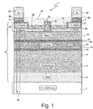
- Figure 1 is a sectional view of a PHEMT power device according to an embodiment of the present invention.
- the PHEMT power device 1 includes a III-V substrate 2, e.g., a semi-insulating GaAs substrate, a doped epitaxial substrate 3 formed on the semi-insulating GaAs substrate 2, and source, drain and gate electrodes 4, 5 and 6 formed on the epitaxial substrate 3.
- a III-V substrate 2 e.g., a semi-insulating GaAs substrate
- a doped epitaxial substrate 3 formed on the semi-insulating GaAs substrate 2
- source, drain and gate electrodes 4, 5 and 6 formed on the epitaxial substrate 3.
- epitaxial substrate 3 comprises an undoped GaAs buffer layer 10; an undoped AlGaAs/GaAs superlattice layer 11; an undoped wide-bandgap AlGaAs layer 12; a first ultrathin doped silicon (pulse) electron supply (donor) layer 13, a first spacer layer 14, an undoped narrow-bandgap InGaAs electron transit (channel) layer 15, a second spacer layer 16, a second ultrathin silicon doped (pulse) electron supply (donor) layer 17 with a different doping concentration than the first electron supply layer 13, an undoped or lightly doped wide-bandgap Schottky AlGaAs layer 18, and a GaAs (ohmic) contact (cap) layer 19 sequentially stacked on the semi-insulating GaAs substrate 2.
- GaAs contact layer 19 is doped and includes a lower lightly doped GaAs contact layer 20 and an upper highly doped GaAs contact layer 21.
- doped GaAs contact layer 19 is approximately 100 nm thick
- lightly doped GaAs contact layer 20 is approximately 30 nm thick and is formed to have a doping concentration of approximately 3.10 17 cm -3
- highly doped GaAs contact layer 21 is approximately 70 nm thick and is formed to have a doping concentration of approximately 3.5 ⁇ 10 18 cm -3 .
- Undoped AlGaAs layer 12 is approximately 4 nm thick and contains aluminum (Al) approximately ranging from 22% to 24% by mole ratio
- InGaAs electron transit layer 15 is approximately 13-15 nm thick and contains indium (In) ranging approximately from 15% to 20% by mole ratio
- lightly doped AlGaAs layer 18 is approximately 30 nm thick, contains aluminum (Al) approximately ranging from 22% to 24% by mole ratio, and is formed to have a doping concentration ranging approximately from 1.0.10 17 to 3.0 ⁇ 10 17 cm -3 .
- the first electron supply layer 13 has a lower doping concentration than the second electron supply layer 17. Additionally, in order to have a doping level in the InGaAs electron transit layer 15 approximately ranging from 1.7 ⁇ 10 12 to 2.7 ⁇ 10 12 cm -2 , first electron supply layer 13 is formed to have a doping level of approximately 1 ⁇ 10 12 cm -2 , and second electron supply layer 17 is formed to have a doping level of approximately 5 ⁇ 10 12 cm -2 . Additionally, the first and the second electron supply layers 13, 17 are each approximately 0.5 nm thick.
- an Au/Ge/Ni/Au metallization is deposited on the highly doped GaAs contact layer 21 and subjected to rapid thermal annealing (RTA) to form source and drain electrodes 4, 5 in ohmic contact with the highly doped GaAs contact layer 21.
- RTA rapid thermal annealing
- epitaxial substrate 3 may be mesa-etched or, preferably, ion implanted using Deuterium or Fluorine high energy ions down to the AlGaAs/GaAs superlattice layer 11.
- doped GaAs contact layer 19 is recess etched to form a double recess structure 22 including an upper wide recess 23 formed in the highly doped GaAs contact layer 21 and a lower narrow recess 24 formed in lightly doped GaAs contact layer 20 and partly in lightly doped AlGaAs layer 18.
- highly doped GaAs contact layer 21 between source and drain electrodes 4, 5 is etched to form wide recess 23, and then lightly doped GaAs contact layer 20 is selectively wet etched inside the wide recess 23 down to lightly doped AlGaAs layer 18 to form narrow recess 24.
- selective etching is carried out using a ph-controlled and temperature-controlled citric acid and hydrogen peroxide solution.
- each one of the two etchings are performed by patterning lightly and highly doped GaAs contact layers 20, 21 with positive i-line photoresists. Presence of the lightly doped AlGaAs layer 18 ensures etching uniformity even in wet etching performed to form the double recess during the manufacture of the PHEMT power device 1.
- gate electrode 6 is then formed in contact with the AlGaAs Schottky layer 18 by evaporating titanium (Ti) and aluminium (Al) on an exposed surface of lightly doped AlGaAs layer 18.
- gate electrode 6 extends centrally in double recess 22 from AlGaAs Schottky layer 18 and through both lightly and highly doped lower GaAs contact layers 20, 21 and protrudes outside double recess 22.
- PECVD Plasma Enhanced Chemical Vapour Deposition
- a Ti/Pt/Au base metal layer 26 is then formed, for example by evaporation, and then layered on source and drain electrodes 4, 5, and an Au layer 27 is then formed, for example by electroplating, on the base metal layer 26.
- Base metal layer 26 defines an interdiffusion barrier that isolates ohmic contact and prevents gold from diffusing from Au-plated layer 27 to source and gate electrodes 4, 5.
- Source and drain electrodes 4, 5 are then connected to respective source and drain pads (not shown) via Au-plated airbridges (not shown).
- semi-insulating GaAs substrate 2 is thinned down from an initial thickness of approximately 650 ⁇ m to a final thickness ranging approximately from 50 to 120 ⁇ m, and then the PHEMT 1 is back-etched to form a via-hole 28, which is metallized, including a surrounding area, with a thick Au layer to extend from thinned semi-insulating GaAs substrate 2 up to source electrode 4 for source pad interconnection, in order to minimize the parasitic source-to-ground inductances, and heat sink provision.
- FIG. 2 is a sectional view of a PHEMT power device similar to that shown in Figure 1 , where same reference numerals designate same elements.
- PHEMT power device shown in Figure 2 designated by 1', differs from PHEMT power device 1 shown in Figure 1 in that gate electrode 6 is generally T-shaped with a lower leg portion 6a formed of Ti and an upper head portion 6b formed of A1. More in detail, leg portion 6a of gate electrode 6 has an height substantially equal to depth of double recess 22, so that head portion 6b of gate electrode 6 protrudes outside double recess 22.
- the T shape is obtained by dry-etching the Ti of the gate metal stack in a suitable Fluorine/Oxygen plasma chemistry in low-damage isotropic plasma-etch reactor.
- the Fluorine gas carrier could be CF 4 , or CHF 3 or SF 6 .
- the oxygen carrier gas could be O 2 .
- the Plasma is created by an RF discharge in a Plasma Etch parallel plate configuration.
- Each plate of the chamber is heated, for example in the range 100 to 200 °C, the chamber pressure is in the range 200 to 1000 mTorr.
- RF power discharge should be lowered to reduce as much as possible surface damage caused by ion and electron bombardment.
- the RF power discharge must be lower than 50 Watt.
- ECR Electron Cyclotron Resonance, ICP - Inductively Coupled Plasma.
- the Al of the head portion 6b of the gate electrode 6 is used as a mask layer because the Al becomes fluorinated and remains un-etched by the Fluorine plasma. So, the head portion 6b of the gate electrode 6, made of Al, stays un-etched, while the leg portion 6a of the of the gate electrode 6, made of Ti and lying on the AlGaAs Schottky layer 18, becomes laterally etched. In this way a gate length down to 0.15 ⁇ m can be obtained with a quick and low-cost manufacturing process, keeping a low gate finger resistance.
- FIG 3 is a sectional view of a PHEMT power device similar to those shown in Figures 1 and 2 , where same reference numerals designate same elements.
- PHEMT power device shown in Figure 3 designated by 1" differs from PHEMT power devices shown in Figures 1 and 2 in that it is provided with a field plate 29 connected to the gate electrode 6 and extending toward the drain electrode 5 without overlapping either the highly doped contact layer 21 or the drain electrode (5).
- the field plate 29 is formed as a gate extension 6c coplanar with highly doped GaAs contact layer 21, vertically overlapping part of protective insulating layer 25 on the lightly doped GaAs contact layer 20, and ending at a distance of 1.0 ⁇ m from highly doped lower GaAs contact layer 21.
- the protective insulating layer 25 made of silicon nitride (Si 3 N 4 ) is ultrathin (less than 50 nm), and is deposited by PECVD so optimized to reach a high dielectric constant of the Si 3 N 4 , and to control the GaAs/Si 3 N 4 interface states.
- AlGaAs layer 18 is the donor layer, and in the final PHEMT power device this layer should be depleted from Schottky gate 6 to AlGaAs/GaAs interface to eliminate any effect of parallel conduction in AlGaAs otherwise detrimental to PHEMT performance.
- this layer must be considered that increasing the doping level in the donor layer reduces the breakdown voltage of the PHEMT.
- a pulsed doped, ⁇ doped AlGaAs layer is possible to use of a Si monolayer, approximately 0.5 nm thick, with a very high doping level.
- GaAs buffer layer 10 because of drain to source electric field, part of electrons can be injected into GaAs buffer layer 10. This phenomenon induces a gain reduction as a result of increasing drain output conductance.
- electron injection into the GaAs buffer layer 10 is controlled by means of AlGaAs/GaAs superlattice layer 11 into GaAs buffer layer 10, that at the same time does not change channel quality.
- the PHEMT power device with different gate length according to the present invention has a pinch-off voltage approximately from - 0.8V to -0.6V, a saturation current ranging from 100 to 300 mA/mm at a gate voltage of 0V, and a maximum saturation current ranging from 300 to 600 mA/mm at a gate voltage of 0.8V.
- transconductance is nearly consistent in the range of 250-350 mS/mm at a gate voltage ranging from 0 to 1V.
- the PHEMT power device exhibits improved linearity.
- the PHEMT power device according to the present invention exhibits a low knee voltage of about 1V and an off-state breakdown voltage of about 18V without a field-plate structure and of 40V with a field-plate structure, while maximum current remained unaffected. This result explains that a high gate drain breakdown voltage can be obtained keeping low ohmic contact resistance.
- the PHEMT power device has an output power up to 29 dBm/mm with an associated power gain up to 12 dB, which power characteristics have been determined by a load-pull method at a typical value of 1 dB of gain compression up to a frequency of 10 GHz if the gate length is conveniently adapted.
- power performance are additionally increased achieving an output power up to 32 dBm/mm and an associated power gain up to 15 dB for C band applications.
- the PHEMT power device may be used to amplify signals up to 40GHz by appropriately varying the gate length.
- the formation of a doped GaAs contact layer 19, particularly made up of a lower lightly doped lower GaAs contact layer 20 and an upper highly doped lower GaAs contact layer 21 in ohmic contact with the source and drain electrodes allows the contact resistance therebetween to be lowered, thus improving voltage characteristics of the PHEMT.
- a double recess structure 22 made up of an upper wide recess 23 formed in upper highly doped GaAs contact layer 21 and of a lower narrow recess 24 formed in lower lightly doped GaAs contact layer 20 allows for the ohmic contact to be placed on highly doped GaAs contact layer 21, thus improving the overall power characteristics of the PHEMT, in particular significantly increasing the breakdown voltage while maintaining a low knee voltage, and improving linearity and power-added efficiency.
- the combination of the double recess structure 22 with the lightly and highly doped GaAs contact layers 20, 21 allows the PHEMT power device to operate with a single voltage supply, without any need for a negative bias voltage to the gate contact.
- the PHEMT of the present invention allows the Class A amplifier requirements to be fulfilled with the gate contact pad directly connected to ground.
- the doped silicon layer 13 with a lower doping concentration than the doped silicon layer 17 makes the transconductance of the PHEMT power device invariant with respect to gate-to-source voltages, while the lightly doped AlGaAs layer 18 ensures etching uniformity in wet recess etching performed to manufacture the PHEMT power device, thus making the overall manufacturing process for the PHEMT power device easy and hence improving the productivity.
- a T-gate structure allows gate-to-source capacitance and gate finger resistance to be significantly reduced, allowing the PHEMT to achieve operating frequencies up to 40 GHz.
- the undoped wide-bandgap AlGaAs layer 12 and the first ultrathin doped silicon electron supply layer 13 may be replaced with a single uniformly doped AlGaAs electron supply layer.
Landscapes
- Junction Field-Effect Transistors (AREA)
- Electrodes Of Semiconductors (AREA)
Description
- The present invention relates in general to a power device, and more particularly to a pseudomorphic high electron mobility transistor (PHEMT) power device and to a process for manufacturing the same.
- As is known, pseudomorphic high electron mobility transistors (PHEMTs) are extensively used in wireless communication systems for switching, power and low noise amplifier applications. These transistors find wide market acceptance because of their high RF gain and power added efficiency (PAE) and low noise figure (NF). The excellent properties of these transistors also make them attractive for use in satellite communication systems including direct broadcast satellite television (DBS-TV) and global satellite communication systems. PHEMT technology is also used in high-speed analog and digital IC's such as 2.5-10 Gb/s lightwave communication systems. The higher frequency response of PHEMTs are currently finding use in millimeter wave communications (40 Gb/s) and radar systems.
- The increasing market demand for RF power devices with higher and higher performance for wireless communication systems, radar detection, satellite and electronic warfare systems has led the electronics industry to extend the operating frequencies of available power devices and technologies. To increase operating frequencies of power devices up to the millimeter wave range, several key technological features have been proposed including an optimized PHEMT epitaxial layer structure, an optimized device layout of the unit cell for specific applications, and thin-film technology development adequate for high frequency functions. In particular, the most significant requirement set for the epitaxial layer structure is associated with the condition of ensuring that free electrons in the conductive channel are physically separated from ionized donors. This solution allows for a significant reduction in ionized impurity scattering, enhancing electron mobility and therefore marked performance improvements over conventional metal-semiconductor field effect transistors (MESFET).
- Additionally, pseudomorphic high electron mobility transistors PHEMTs usually require a negative gate voltage bias to operate (see for example
US 2002/024057 A1 ). Therefore, as compared to heterojunction bipolar transistors (HBTs) that use a positive gate voltage, the introduction of such a negative voltage disadvantageously requires a dedicated voltage supply circuit that increases chip complexity and manufacturing costs. - A PHEMT power device capable of operating with a single voltage supply is for example disclosed in
US 2003/122152 A1 . The PHEMT power device includes an epitaxial substrate including a GaAs buffer layer, an AlGaAs/GaAs superlattice layer, an undoped AlGaAs layer, a first doped silicon layer, a first spacer, an InGaAs electron transit layer, a second spacer, a second doped silicon layer having a different doping concentration from the first doped silicon layer, a lightly doped AlGaAs layer, and an undoped GaAs cap layer stacked sequentially on a semi-insulating GaAs substrate; a source electrode and a drain electrode formed on and in ohmic contact with the undoped GaAs cap layer; and a gate electrode formed on the lightly doped AlGaAs layer to extend through the undoped GaAs cap layer. -
EP 0 514 079 A2 discloses a high electron mobility transistor which includes a pair of charge screen layers disposed over a first one of active and charge donor layers of the high electron mobility transistor. The two screen layers are patterned to provide a double recessed channel. A first charge screen layer disposed adjacent to the charge donor layer is etched to provide a recess having a first length between source and drain electrodes, whereas a second charge screen layer disposed over the first aforementioned charge screen layer and a portion of the aforementioned first charge screen layer are etched to provide a second, substantially longer length between source and drain electrodes. The gate electrode is provided in the first aforementioned recess in Schottky barrier contact with the charge donor layer. -
WO 2004/025707 A discloses a semiconductor structure that integrates wide bandgap semiconductors with silicon. The semiconductor structure includes: a substrate; a SiCAIN region formed over the substrate, and an active region formed over the SiCAIN region. The substrate can comprise silicon, silicon carbide (SiC) or silicon germanium (SiGe). The active region can include a gallium nitride material region, such as GaN, AlGaN, InGaN or AlInGaN. It also can include AIN and InN region. The structure also can include a crystalline oxide interface formed between the substrate and the SiCAIN region. A preferred crystalline oxide interface is Si-Al-O-N. The active layer can be formed by known fabrication processes, including metal organic chemical vapor deposition or by atomic layer epitaxy. The crystalline oxide interface is normally formed by growing SiCAIN on Si(111) via a crystalline oxide interface, but can also be formed by metal organic chemical vapor deposition or by atomic layer epitaxy. - The Applicant has noticed that in order to provide a PHEMT power device operable with a single voltage supply (the drain supply voltage only), it is necessary to optimize the pinch-off voltage that permits to achieve class A operating conditions (drain-to-source current equal to half of the maximum achievable one) while maintaining the gate grounded without any bias.
- In particular, the Applicant has noticed that an optimized PHEMT power device having excellent linearity and power-added efficiency, high breakdown voltage, and capable of operating with a single voltage supply should meet the following requirements: a low knee voltage, a high and uniform transconductance, and a low source-gate capacitance.
- In this respect, the Applicant has noticed that even if the PHEMT power device disclosed in
US 2003/122152 A1 is operable with a single voltage supply, its performance proves however to be satisfactory only in the C frequency band (4 to 6 GHz), while becomes quite unsatisfactory in the X frequency band (8.0 to 12.0 GHz), and the PHEMT power device is completely unusable in the Ka (K-above) frequency band (18 to 40 GHz). - Therefore, the Applicant has noticed that in order to provide a PHEMT power device operable with a single voltage supply and having also excellent performance in the X frequency band and the Ka frequency band, it is necessary to further optimize the structure of the dedicated epitaxial substrate and, consequently, the device manufacturing process disclosed in
US2003/122152 A1 . - The main objective of present invention is therefore to provide a PHEMT power device operable with a single voltage supply, suitable for a satisfactory use in highfrequency digital wireless communications, in particular which may be used to amplify signals up to 40GHz, i.e., for example C frequency band, X frequency band and Ka frequency band, and having a higher linearity, breakdown voltage and power-added efficiency than the PHEMTs in the prior art.
- Another objective of present invention is to provide a process for manufacturing this PHEMT power device.
- These objectives are achieved by the present invention in that it relates to a PHEMT power device and to a process for manufacturing the same, as defined in the appended claims.
- The present invention achieves the aforementioned objective by exploiting advances in epitaxial growth technologies of III-V semiconductor heterojunctions, which advances ensure the possibility of engineering the band structure, doping type and level in different regions of semiconductor devices, and by adopting new semiconductor materials with superior electrical characteristics, such as wide band-gap semiconductor, and by properly designing the PHEMT structure. Use of these additional degrees of freedom provides the opportunity of developing new devices with considerable improvement in RF performance. In particular, the present invention achieves the aforementioned objective by introducing an optimized epilayer sequence and a double recessed gate geometry. More in detail, the present invention achieves the aforementioned objective by providing a pseudomorphic high electron mobility transistor (PHEMT) power device including:
- a semi-insulating substrate;
- an epitaxial substrate formed on the semi-insulating substrate; the epitaxial substrate including a buffer layer, a superlattice layer, a first electron supply layer, a first spacer layer, an electron transit layer, a second spacer layer, a second electron supply layer, a Schottky layer, and a contact layer sequentially stacked on the semi-insulating substrate; wherein the first electron supply layer has a lower doping concentration then the second electron supply layer;
- source and drain electrodes formed on, and in ohmic contact with the contact layer; and
- a gate electrode formed on the Schottky layer to extend through the contact layer;
- wherein the contact layer includes:
- a lightly doped contact layer formed on the Schottky layer;
- a highly doped contact layer formed on the lightly doped contact layer and having a doping concentration higher than the lightly doped contact layer;
- wherein the PHEMT power device further comprises:
- a wide recess formed to penetrate the highly doped contact layer so as to expose a surface of the lightly doped contact layer; and
- a narrow recess formed in the wide recess to penetrate the lightly doped contact layer so as to expose a surface of the Schottky layer;
- wherein the gate electrode is formed in the narrow recess and in Schottky contact with the Schottky layer to extend from the exposed surface of the Schottky layer through the lightly and highly doped contact layers; and
- the source and drain electrodes are formed on, and in ohmic contact with the highly doped contact layer outside the wide recess so that the wide recess is arranged between the source and drain electrodes.
- For a better understanding of the present invention, preferred embodiments, which are intended purely by way of example and are not to be construed as limiting, will now be described with reference to the attached drawings, wherein:
-
Figure 1 is a sectional view of a PHEMT power device according to an embodiment of the present invention; -
Figure 2 is a sectional view of a PHEMT power device according to another embodiment of the present invention; and -
Figure 3 is a sectional view of the PHEMT power device according to a different embodiment of the present invention. - The following discussion is presented to enable a person skilled in the art to make and use the invention. Various modifications to the embodiments will be readily apparent to those skilled in the art, and the generic principles herein may be applied to other embodiments and applications without departing from the spirit and scope of the present invention. Thus, the present invention is not intended to be limited to the embodiments shown, but is to be accorded the widest scope consistent with the principles and features disclosed herein and defined in the attached claims.
-
Figure 1 is a sectional view of a PHEMT power device according to an embodiment of the present invention. - The PHEMT
power device 1 includes a III-V substrate 2, e.g., a semi-insulating GaAs substrate, a dopedepitaxial substrate 3 formed on thesemi-insulating GaAs substrate 2, and source, drain andgate electrodes epitaxial substrate 3. - In particular,
epitaxial substrate 3 comprises an undoped GaAsbuffer layer 10; an undoped AlGaAs/GaAssuperlattice layer 11; an undoped wide-bandgap AlGaAslayer 12; a first ultrathin doped silicon (pulse) electron supply (donor)layer 13, afirst spacer layer 14, an undoped narrow-bandgap InGaAs electron transit (channel)layer 15, asecond spacer layer 16, a second ultrathin silicon doped (pulse) electron supply (donor)layer 17 with a different doping concentration than the firstelectron supply layer 13, an undoped or lightly doped wide-bandgap SchottkyAlGaAs layer 18, and a GaAs (ohmic) contact (cap)layer 19 sequentially stacked on thesemi-insulating GaAs substrate 2. - In order to lower ohmic contact resistance between
GaAs contact layer 19 and source anddrain electrodes GaAs contact layer 19 is doped and includes a lower lightly dopedGaAs contact layer 20 and an upper highly dopedGaAs contact layer 21. In particular, dopedGaAs contact layer 19 is approximately 100 nm thick, lightly dopedGaAs contact layer 20 is approximately 30 nm thick and is formed to have a doping concentration of approximately 3.1017 cm-3, and highly dopedGaAs contact layer 21 is approximately 70 nm thick and is formed to have a doping concentration of approximately 3.5·1018cm-3. -
Undoped AlGaAs layer 12 is approximately 4 nm thick and contains aluminum (Al) approximately ranging from 22% to 24% by mole ratio, InGaAselectron transit layer 15 is approximately 13-15 nm thick and contains indium (In) ranging approximately from 15% to 20% by mole ratio; and lightly dopedAlGaAs layer 18 is approximately 30 nm thick, contains aluminum (Al) approximately ranging from 22% to 24% by mole ratio, and is formed to have a doping concentration ranging approximately from 1.0.1017 to 3.0·1017 cm-3. - In order to improve transconductance linearity, the first
electron supply layer 13 has a lower doping concentration than the secondelectron supply layer 17. Additionally, in order to have a doping level in the InGaAselectron transit layer 15 approximately ranging from 1.7·1012 to 2.7·1012 cm-2, firstelectron supply layer 13 is formed to have a doping level of approximately 1·1012 cm-2, and secondelectron supply layer 17 is formed to have a doping level of approximately 5·1012 cm-2. Additionally, the first and the second electron supply layers 13, 17 are each approximately 0.5 nm thick. - To obtain Ohmic contact an Au/Ge/Ni/Au metallization is deposited on the highly doped
GaAs contact layer 21 and subjected to rapid thermal annealing (RTA) to form source anddrain electrodes GaAs contact layer 21. - In order to separate active areas of individual PHEMT power devices,
epitaxial substrate 3 may be mesa-etched or, preferably, ion implanted using Deuterium or Fluorine high energy ions down to the AlGaAs/GaAs superlattice layer 11. - After these two steps in order to increase the breakdown voltage and maintain the knee voltage low, while preserving high transconductance and high PHEMT gain, thereby improving the PHEMT power characteristics, doped
GaAs contact layer 19 is recess etched to form adouble recess structure 22 including an upperwide recess 23 formed in the highly dopedGaAs contact layer 21 and a lowernarrow recess 24 formed in lightly dopedGaAs contact layer 20 and partly in lightly dopedAlGaAs layer 18. In particular, to formdouble recess structure 22, highly dopedGaAs contact layer 21 between source anddrain electrodes wide recess 23, and then lightly dopedGaAs contact layer 20 is selectively wet etched inside thewide recess 23 down to lightly dopedAlGaAs layer 18 to formnarrow recess 24. In particular, selective etching is carried out using a ph-controlled and temperature-controlled citric acid and hydrogen peroxide solution. Additionally, each one of the two etchings are performed by patterning lightly and highly doped GaAs contact layers 20, 21 with positive i-line photoresists. Presence of the lightly dopedAlGaAs layer 18 ensures etching uniformity even in wet etching performed to form the double recess during the manufacture of thePHEMT power device 1. - After formation of
double recess 22,gate electrode 6 is then formed in contact with theAlGaAs Schottky layer 18 by evaporating titanium (Ti) and aluminium (Al) on an exposed surface of lightly dopedAlGaAs layer 18. In particular,gate electrode 6 extends centrally indouble recess 22 fromAlGaAs Schottky layer 18 and through both lightly and highly doped lower GaAs contact layers 20, 21 and protrudes outsidedouble recess 22. - A protective insulating
layer 25, for example made of silicon nitride (Si3N4), is then formed, for example by Plasma Enhanced Chemical Vapour Deposition (PECVD), on a surface of the highly dopedGaAs contact layer 21 exposed by source, drain andgate electrodes - A Ti/Pt/Au
base metal layer 26 is then formed, for example by evaporation, and then layered on source anddrain electrodes Au layer 27 is then formed, for example by electroplating, on thebase metal layer 26.Base metal layer 26 defines an interdiffusion barrier that isolates ohmic contact and prevents gold from diffusing from Au-platedlayer 27 to source andgate electrodes - Source and
drain electrodes - Finally,
semi-insulating GaAs substrate 2 is thinned down from an initial thickness of approximately 650 µm to a final thickness ranging approximately from 50 to 120 µm, and then thePHEMT 1 is back-etched to form a via-hole 28, which is metallized, including a surrounding area, with a thick Au layer to extend from thinnedsemi-insulating GaAs substrate 2 up tosource electrode 4 for source pad interconnection, in order to minimize the parasitic source-to-ground inductances, and heat sink provision. -
Figure 2 is a sectional view of a PHEMT power device similar to that shown inFigure 1 , where same reference numerals designate same elements. In particular, PHEMT power device shown inFigure 2 , designated by 1', differs fromPHEMT power device 1 shown inFigure 1 in thatgate electrode 6 is generally T-shaped with alower leg portion 6a formed of Ti and anupper head portion 6b formed of A1. More in detail,leg portion 6a ofgate electrode 6 has an height substantially equal to depth ofdouble recess 22, so thathead portion 6b ofgate electrode 6 protrudes outsidedouble recess 22. More in detail, the T shape is obtained by dry-etching the Ti of the gate metal stack in a suitable Fluorine/Oxygen plasma chemistry in low-damage isotropic plasma-etch reactor. The Fluorine gas carrier could be CF4, or CHF3 or SF6. The oxygen carrier gas could be O2. - The Plasma is created by an RF discharge in a Plasma Etch parallel plate configuration. Each plate of the chamber is heated, for example in the range 100 to 200 °C, the chamber pressure is in the range 200 to 1000 mTorr. RF power discharge should be lowered to reduce as much as possible surface damage caused by ion and electron bombardment. When a Plasma Etch parallel plate configuration is utilised for this gate etch the RF power discharge must be lower than 50 Watt. Furthermore, better results are achievable if equipment able to ensure cold plasma are introduced (ECR - Electron Cyclotron Resonance, ICP - Inductively Coupled Plasma).
- In such a process, the Al of the
head portion 6b of thegate electrode 6 is used as a mask layer because the Al becomes fluorinated and remains un-etched by the Fluorine plasma. So, thehead portion 6b of thegate electrode 6, made of Al, stays un-etched, while theleg portion 6a of the of thegate electrode 6, made of Ti and lying on theAlGaAs Schottky layer 18, becomes laterally etched. In this way a gate length down to 0.15 µm can be obtained with a quick and low-cost manufacturing process, keeping a low gate finger resistance. -
Figure 3 is a sectional view of a PHEMT power device similar to those shown inFigures 1 and2 , where same reference numerals designate same elements. In particular, PHEMT power device shown inFigure 3 , designated by 1", differs from PHEMT power devices shown inFigures 1 and2 in that it is provided with afield plate 29 connected to thegate electrode 6 and extending toward thedrain electrode 5 without overlapping either the highly dopedcontact layer 21 or the drain electrode (5). In particular, thefield plate 29 is formed as agate extension 6c coplanar with highly dopedGaAs contact layer 21, vertically overlapping part of protective insulatinglayer 25 on the lightly dopedGaAs contact layer 20, and ending at a distance of 1.0 µm from highly doped lowerGaAs contact layer 21. The protective insulatinglayer 25 made of silicon nitride (Si3N4) is ultrathin (less than 50 nm), and is deposited by PECVD so optimized to reach a high dielectric constant of the Si3N4, and to control the GaAs/Si3N4 interface states. - In the PHEMT power devices shown in
Figures 1 ,2 , and3 different GaAs and AlGaAs layers are provided, but the heterojunction of greatest interest is that between silicon dopedAlGaAs layer undoped InGaAs layer 15. In fact, due to the higher bandgap of AlGaAs layer compared to the adjacent InGaAs layer, free electrons diffuse into the InGaAs layer and form a two dimensional electron gas (2-DEG) at the heterointerface, where they remain confined in a very thin sheet, and transport properties of the 2-DEG are much better than those of free electrons in a conventional MESFET. -
AlGaAs layer 18 is the donor layer, and in the final PHEMT power device this layer should be depleted fromSchottky gate 6 to AlGaAs/GaAs interface to eliminate any effect of parallel conduction in AlGaAs otherwise detrimental to PHEMT performance. During heterostructure design, it must be considered that increasing the doping level in the donor layer reduces the breakdown voltage of the PHEMT. To overcome this difficulty while maintaining a high 2-DEG sheet carrier concentration, it is possible to use a pulsed doped, δ doped AlGaAs layer. This solution makes use of a Si monolayer, approximately 0.5 nm thick, with a very high doping level. - As for thickness of spacer layers 14, 16, even though free electrons are physically separated from donors, close proximity produces an electrostatic interaction, known as Coulomb Scattering. This effect is reduced by separating the 2-DEG from the AlGaAs donor layer by means of a thin spacer layer of undoped AlGaAs. It is worthwhile to mention that noise performance of a PHEMT is strictly connected to spacer thickness.
- As for
GaAs buffer layer 10, because of drain to source electric field, part of electrons can be injected intoGaAs buffer layer 10. This phenomenon induces a gain reduction as a result of increasing drain output conductance. In the PHEMTs, electron injection into theGaAs buffer layer 10 is controlled by means of AlGaAs/GaAs superlattice layer 11 intoGaAs buffer layer 10, that at the same time does not change channel quality. - Described here below are results of characteristic measurements carried out on a PHEMT power device manufactured according to the present invention and with a 0.5-µm-gate length, 0.25-µm-gate length and with a field-plate structure. All the mentioned results are referred to a 100-µm-unit gate width and for 1-mm-total gate width. In particular, as far as transconductance and saturation current are concerned, the PHEMT power device with different gate length according to the present invention has a pinch-off voltage approximately from - 0.8V to -0.6V, a saturation current ranging from 100 to 300 mA/mm at a gate voltage of 0V, and a maximum saturation current ranging from 300 to 600 mA/mm at a gate voltage of 0.8V. In addition, transconductance is nearly consistent in the range of 250-350 mS/mm at a gate voltage ranging from 0 to 1V. As a result, the PHEMT power device exhibits improved linearity. As far as current-voltage characteristic is concerned, the PHEMT power device according to the present invention exhibits a low knee voltage of about 1V and an off-state breakdown voltage of about 18V without a field-plate structure and of 40V with a field-plate structure, while maximum current remained unaffected. This result explains that a high gate drain breakdown voltage can be obtained keeping low ohmic contact resistance. As far as power characteristics are concerned, the PHEMT power device according to the present invention has an output power up to 29 dBm/mm with an associated power gain up to 12 dB, which power characteristics have been determined by a load-pull method at a typical value of 1 dB of gain compression up to a frequency of 10 GHz if the gate length is conveniently adapted. Introducing the field-plate structure, power performance are additionally increased achieving an output power up to 32 dBm/mm and an associated power gain up to 15 dB for C band applications. Finally, as far as high RF amplifier applications are concerned, the PHEMT power device according to the present invention may be used to amplify signals up to 40GHz by appropriately varying the gate length.
- The advantages of the present invention are evident from the foregoing. In particular, in the PHEMT power device according to the present invention, the formation of a doped
GaAs contact layer 19, particularly made up of a lower lightly doped lowerGaAs contact layer 20 and an upper highly doped lowerGaAs contact layer 21 in ohmic contact with the source and drain electrodes allows the contact resistance therebetween to be lowered, thus improving voltage characteristics of the PHEMT. - Additionally, the formation of a
double recess structure 22 made up of an upperwide recess 23 formed in upper highly dopedGaAs contact layer 21 and of a lowernarrow recess 24 formed in lower lightly dopedGaAs contact layer 20 allows for the ohmic contact to be placed on highly dopedGaAs contact layer 21, thus improving the overall power characteristics of the PHEMT, in particular significantly increasing the breakdown voltage while maintaining a low knee voltage, and improving linearity and power-added efficiency. - Moreover, the combination of the
double recess structure 22 with the lightly and highly doped GaAs contact layers 20, 21 allows the PHEMT power device to operate with a single voltage supply, without any need for a negative bias voltage to the gate contact. - Further, the PHEMT of the present invention allows the Class A amplifier requirements to be fulfilled with the gate contact pad directly connected to ground.
- Yet further, the doped
silicon layer 13 with a lower doping concentration than the dopedsilicon layer 17 makes the transconductance of the PHEMT power device invariant with respect to gate-to-source voltages, while the lightly dopedAlGaAs layer 18 ensures etching uniformity in wet recess etching performed to manufacture the PHEMT power device, thus making the overall manufacturing process for the PHEMT power device easy and hence improving the productivity. - Finally, a T-gate structure allows gate-to-source capacitance and gate finger resistance to be significantly reduced, allowing the PHEMT to achieve operating frequencies up to 40 GHz.
- Finally, numerous modifications and variants can be made to the present invention, all falling within the scope of the invention, as defined in the appended claims.
- For example, the undoped wide-
bandgap AlGaAs layer 12 and the first ultrathin doped siliconelectron supply layer 13 may be replaced with a single uniformly doped AlGaAs electron supply layer.
Claims (33)
- A Ka-band, single-voltage supply pseudomorphic high electron mobility transistor (PHEMT) power device (1; 1'; 1") comprising:a semi-insulating substrate (2);an epitaxial substrate (3) formed on the semi-insulating substrate (2); the epitaxial substrate (3) comprising a buffer layer (10), a superlattice layer (11), a first electron supply layer (12, 13), a first spacer layer (14), an electron transit layer (15), a second spacer layer (16), a second electron supply layer (17), a Schottky layer (18), and a contact layer (19) sequentially stacked on the semi-insulating substrate (2); wherein the first electron supply layer (12, 13) has a lower doping concentration then the second electron supply layer (17);source and drain electrodes (4, 5) formed on, and in ohmic contact with the contact layer (19); anda gate electrode (6) formed on the Schottky layer (18) to extend through the contact layer (19);wherein the contact layer (19) comprises:a lightly doped contact layer (20) formed on the Schottky layer (18); anda highly doped contact layer (21) formed on the lightly doped contact layer (20) and having a doping concentration higher than the lightly doped contact layer (20) ;wherein the PHEMT power device (1) further comprises:a wide recess (23) formed to penetrate the highly doped contact layer (21) so as to expose a surface of the lightly doped contact layer (20); anda narrow recess (24) formed in the wide recess (23) to penetrate the lightly doped contact layer (20) so as to expose a surface of the Schottky layer (18);wherein the gate electrode (6) is formed in the narrow recess (24) and in Schottky contact with the Schottky layer (18) to extend from the exposed surface of the Schottky layer (18) through the lightly and highly doped contact layers (20, 21); andwherein the source and drain electrodes (4, 5) are formed on, and in ohmic contact with the highly doped contact layer (21) outside the wide recess (23) so that the wide recess (23) is arranged between the source and drain electrodes (4, 5).
- The PHEMT power device of claim 1, further including:
a protective insulating layer (25) formed on a surface of the highly doped contact layer (21) exposed by source, drain and gate electrodes (4, 5, 6). - The PHEMT power device of claim 1 or 2, further including:a base metal layer (26) formed on the source and drain electrodes (4, 5); andan Au layer (27) formed on the base metal layer (26).
- The PHEMT power device of any preceding claim, further including:
a metallized via-hole (28) formed to extend from the semi-insulating substrate (2) to the source electrode (4) for source pad interconnection and heat sink provision. - The PHEMT power device of any preceding claim, wherein the gate electrode (6) is generally T-shaped.
- The PHEMT power device of claim 2, further including:
a field plate (29) formed on the protective insulating layer (25), electrically connected to the gate electrode (6) and extending toward the drain electrode (5) without overlapping either the highly doped contact layer (21) or the drain electrode (5). - The PHEMT power device of claim 6, wherein the field plate is formed as a gate extension (6c) which is substantially coplanar with the highly doped GaAs contact layer (21), vertically overlaps part of the lightly doped GaAs contact layer (20), and ends at a distance from the highly doped contact layer (21).
- The PHEMT power device of claim 1, 2 and 3, wherein the substrate (2) is a semi-insulating substrate formed of GaAs, the buffer layer (10) is formed of GaAs, the superlattice layer (11) is formed of AlGaAs/GaAs, the first and second electron supply layers (13, 17) are formed of doped silicon, the electron transit layer (15) is formed of InGaAs; the Schottky layer (18) is formed of AlGaAs, the lightly and highly doped contact layers (21, 22) are formed of GaAs, the gate electrode (6) is formed of Ti/Al, the source and drain electrodes (4, 5) are formed of Au/Ge/Ni/Au metal thin films, the protective insulating layer (25) is formed of silicon nitride, and the base metal layer (26) is formed of Ti/Pt/Au.
- The PHEMT power device of any preceding claim, wherein the lightly doped contact layer (20) has a doping concentration of approximately 3.1017 cm-3, and the highly doped contact layer (21) has a doping concentration of approximately 3.5·1018 cm-3.
- The PHEMT power device of any preceding claim, wherein the first and second electron supply layers (13, 17) are formed to have doping concentrations so as to have a doping level in the electron transit layer (15) approximately ranging from 1.7·1012 to 2.7·1012 cm-2.
- The PHEMT power device of any preceding claim, wherein the first electron supply layer (13) is formed to have a doping level of approximately 1·1012 cm-2, and the second electron supply layer (17) is formed to have a doping level of approximately 5·1012 cm-2.
- The PHEMT power device of any preceding claim, wherein the electron transit layer (15) contains indium ranging approximately from 15% to 20% by mole ratio, the Schottky layer (18) contains aluminum approximately ranging from 22% to 24% by mole ratio, and is formed to have a doping concentration ranging approximately from 1.0·1017 to 3.0·1017 cm-3.
- The PHEMT power device of any preceding claim, wherein the first electron supply layer (12, 13) includes:an undoped wide-bandgap layer (12) formed on the superlattice layer (11); anda doped silicon layer (13) formed on the undoped wide-bandgap layer (12).
- The PHEMT power device of claim 13, wherein the undoped wide-bandgap layer (12) is formed of AlGaAs and contains aluminum approximately ranging from 22% to 24% by mole ratio.
- A process for manufacturing a Ka-band, single-voltage supply pseudomorphic high electron mobility transistor (PHEMT) power device (1; 1'; 1") comprising:providing a semi-insulating substrate (2);forming an epitaxial substrate (3) on the semi-insulating substrate (2), wherein forming an epitaxial substrate (3) comprises sequentially stacking a buffer layer (10), a superlattice layer (11), a first electron supply layer (12, 13), a first spacer layer (14), an electron transit layer (15), a second spacer layer (16), a second electron supply layer (17), a Schottky layer (18), and a contact layer (19) on the semi-insulating substrate (2); wherein the first electron supply layer (12, 13) has a lower doping concentration then the second electron supply layer (17);forming source and drain electrodes (4, 5) on, and in ohmic contact with the contact layer (19); andforming a gate electrode (6) on the Schottky layer (18) to extend through the contact layer (19);wherein forming a contact layer (19) comprises:forming a lightly doped contact layer (20) on the Schottky layer (18);forming a highly doped contact layer (21) on the lightly doped contact layer (20) and having a doping concentration higher than the lightly doped contact layer (20) ;wherein the manufacturing process further comprises:forming a wide recess (23) to penetrate the highly doped contact layer (21) so as to expose a surface of the lightly doped contact layer (20); andforming a narrow recess (24) in the wide recess (23) to penetrate the lightly doped contact layer (20) so as to expose a surface of the Schottky layer (18);wherein the gate electrode (6) is formed in the narrow recess (24) and in Schottky contact with the Schottky layer (18) to extend from the exposed surface of the Schottky layer (18) through the lightly and highly doped contact layers (20, 21); andthe source and drain electrodes (4, 5) are formed on, and in ohmic contact with the highly doped contact layer (21) outside the wide recess (23) so that the wide recess (23) is arranged between the source and drain electrodes (4, 5).
- The process of claim 15, wherein source and drain electrodes (4, 5) are formed before the wide and narrow recesses (20, 21).
- The process of claim 15 or 16, wherein forming source and drain electrodes (4, 5) includes:forming respective metal thin films on the highly doped contact layer (21); andrapidly thermally annealing the deposited metal thin films.
- The process of any preceding claim 15 to 17, further including:
forming a protective insulating layer (25) on a surface of the highly doped contact layer (21) exposed by the source, drain and gate electrodes (4, 5, 6). - The process of any preceding claim 15 to 18, further including:forming a base metal layer (26) on the source and drain electrodes (4, 5); andforming an Au layer (27) on the base metal layer (26) .
- The process of any preceding claim 15 to 19, further including:
forming and metalizing a via-hole (28) to extend from the semi-insulating substrate (2) to the source electrode (4) for source pad interconnection and heat sink provision. - The process of claim 20, wherein forming a via-hole (28) includes:
back-etching the semi-insulating substrate (2) and the epitaxial substrate (3). - The process of claim 20 or 21, further including:
thinning the semi-insulating substrate (2) before formation of the via-hole (28). - The process of any preceding claim 15 to 22, wherein the gate electrode (6) is generally T-shaped.
- The process of claim 23, wherein the T-shaped gate electrode (6) includes a narrow portion (6a) formed of Titanium in the narrow recess (24), and a wide portion (6b) formed of Aluminum outside the narrow recess (24);
and wherein forming the T-shaped gate electrode (6) includes:evaporating the Titanium and the Aluminum on an exposed surface of the Schottky layer (18); anddry-etching the Titanium in a Fluorine/Oxygen plasma. - The process of claim 18, further including:
forming a field plate (29) on the protective insulating layer (25), electrically connected to the gate electrode (6) and extending toward the drain electrode (5) without overlapping either the highly doped contact layer (21) or the drain electrode (5). - The process of claim 25, wherein forming a field plate includes:
forming a gate extension (6c) substantially coplanar with the highly doped GaAs contact layer (21), vertically overlapping part of the lightly doped GaAs contact layer (20), and ending at a distance from the highly doped contact layer (21). - The process of claim 15, 18, and 19, wherein the substrate (2) is a semi-insulating substrate formed of GaAs, the buffer layer (10) is formed of GaAs, the superlattice layer (11) is formed of AlGaAs/GaAs, the first and second electron supply layers (13, 17) are formed of doped silicon, the electron transit layer (15) is formed of InGaAs; the Schottky layer (18) is formed of AlGaAs, the lightly and highly doped contact layers (21, 22) are formed of GaAs, the gate electrode (6) is formed of Ti/Al, the source and drain electrodes (4, 5) are formed of Au/Ge/Ni/Au metal thin films, the protective insulating layer (25) is formed of silicon nitride, and the base metal layer (26) is formed of Ti/Pt/Au.
- The process of any preceding claim 15 to 27, wherein the lightly doped contact layer (20) has a doping concentration of approximately 3·1017 cm-3, and the highly doped contact layer (21) has a doping concentration of approximately 3.5·1018 cm-3.
- The process of any preceding claim 15 to 28, wherein the first and second electron supply layers (13, 17) are formed to have doping concentrations so as to have a doping level in the electron transit layer (15) approximately ranging from 1.7·1012 to 2.7·1012 cm-2.
- The process of any claim 15 to 29, wherein the first electron supply layer (13) is formed to have a doping level of approximately 1·1012 cm-2, and the second electron supply layer (17) is formed to have a doping level of approximately 5·1012 cm-2.
- The process of any preceding claim 15 to 30, wherein the electron transit layer (15) contains indium ranging approximately from 15% to 20% by mole ratio, the Schottky layer (18) contains aluminum approximately ranging from 22% to 24% by mole ratio, and is formed to have a doping concentration ranging approximately from 1.0·1017 to 3.0·1017 cm-3.
- The process of any preceding claim 15 to 31, wherein the first electron supply layer (12, 13) includes:an undoped wide-bandgap layer (12) formed on the superlattice layer (11); anda doped silicon layer (13) formed on the undoped wide-bandgap layer (12).
- The process of claim 32, wherein the undoped wide-bandgap layer (12) is formed of AlGaAs and contains aluminum approximately ranging from 22% to 24% by mole ratio.
Priority Applications (1)
| Application Number | Priority Date | Filing Date | Title |
|---|---|---|---|
| PL06821723T PL2080228T3 (en) | 2006-10-04 | 2006-10-04 | HIGH ELECTRON MOBILITY PSEUDOMORPHIC TRANSISTOR DEVICE (PHEMT) WITH SINGLE VOLTAGE POWER SUPPLY AND THE METHOD OF ITS MANUFACTURING |
Applications Claiming Priority (1)
| Application Number | Priority Date | Filing Date | Title |
|---|---|---|---|
| PCT/IT2006/000705 WO2008041249A1 (en) | 2006-10-04 | 2006-10-04 | Single voltage supply pseudomorphic high electron mobility transistor (phemt) power device and process for manufacturing the same |
Publications (2)
| Publication Number | Publication Date |
|---|---|
| EP2080228A1 EP2080228A1 (en) | 2009-07-22 |
| EP2080228B1 true EP2080228B1 (en) | 2020-12-02 |
Family
ID=38043017
Family Applications (1)
| Application Number | Title | Priority Date | Filing Date |
|---|---|---|---|
| EP06821723.1A Active EP2080228B1 (en) | 2006-10-04 | 2006-10-04 | Single voltage supply pseudomorphic high electron mobility transistor (phemt) power device and process for manufacturing the same |
Country Status (9)
| Country | Link |
|---|---|
| US (1) | US8120066B2 (en) |
| EP (1) | EP2080228B1 (en) |
| JP (1) | JP2010506397A (en) |
| CN (1) | CN101636843B (en) |
| ES (1) | ES2837454T3 (en) |
| PL (1) | PL2080228T3 (en) |
| PT (1) | PT2080228T (en) |
| TW (1) | TWI433317B (en) |
| WO (1) | WO2008041249A1 (en) |
Families Citing this family (59)
| Publication number | Priority date | Publication date | Assignee | Title |
|---|---|---|---|---|
| US7573078B2 (en) * | 2004-05-11 | 2009-08-11 | Cree, Inc. | Wide bandgap transistors with multiple field plates |
| US7550783B2 (en) * | 2004-05-11 | 2009-06-23 | Cree, Inc. | Wide bandgap HEMTs with source connected field plates |
| US9773877B2 (en) * | 2004-05-13 | 2017-09-26 | Cree, Inc. | Wide bandgap field effect transistors with source connected field plates |
| US8981876B2 (en) | 2004-11-15 | 2015-03-17 | Avago Technologies General Ip (Singapore) Pte. Ltd. | Piezoelectric resonator structures and electrical filters having frame elements |
| US7791434B2 (en) * | 2004-12-22 | 2010-09-07 | Avago Technologies Wireless Ip (Singapore) Pte. Ltd. | Acoustic resonator performance enhancement using selective metal etch and having a trench in the piezoelectric |
| US11791385B2 (en) * | 2005-03-11 | 2023-10-17 | Wolfspeed, Inc. | Wide bandgap transistors with gate-source field plates |
| JP5105160B2 (en) * | 2006-11-13 | 2012-12-19 | クリー インコーポレイテッド | Transistor |
| US7884394B2 (en) * | 2009-02-09 | 2011-02-08 | Transphorm Inc. | III-nitride devices and circuits |
| US8902023B2 (en) | 2009-06-24 | 2014-12-02 | Avago Technologies General Ip (Singapore) Pte. Ltd. | Acoustic resonator structure having an electrode with a cantilevered portion |
| US8248185B2 (en) | 2009-06-24 | 2012-08-21 | Avago Technologies Wireless Ip (Singapore) Pte. Ltd. | Acoustic resonator structure comprising a bridge |
| WO2010151721A1 (en) * | 2009-06-25 | 2010-12-29 | The Government Of The United States Of America, As Represented By The Secretary Of The Navy | Transistor with enhanced channel charge inducing material layer and threshold voltage control |
| US8324661B2 (en) * | 2009-12-23 | 2012-12-04 | Intel Corporation | Quantum well transistors with remote counter doping |
| US8796904B2 (en) | 2011-10-31 | 2014-08-05 | Avago Technologies General Ip (Singapore) Pte. Ltd. | Bulk acoustic resonator comprising piezoelectric layer and inverse piezoelectric layer |
| US9243316B2 (en) | 2010-01-22 | 2016-01-26 | Avago Technologies General Ip (Singapore) Pte. Ltd. | Method of fabricating piezoelectric material with selected c-axis orientation |
| US8860120B2 (en) * | 2010-09-22 | 2014-10-14 | Nxp, B.V. | Field modulating plate and circuit |
| US8962443B2 (en) | 2011-01-31 | 2015-02-24 | Avago Technologies General Ip (Singapore) Pte. Ltd. | Semiconductor device having an airbridge and method of fabricating the same |
| JP5776217B2 (en) * | 2011-02-24 | 2015-09-09 | 富士通株式会社 | Compound semiconductor device |
| US9136818B2 (en) | 2011-02-28 | 2015-09-15 | Avago Technologies General Ip (Singapore) Pte. Ltd. | Stacked acoustic resonator comprising a bridge |
| US9425764B2 (en) | 2012-10-25 | 2016-08-23 | Avago Technologies General Ip (Singapore) Pte. Ltd. | Accoustic resonator having composite electrodes with integrated lateral features |
| US9148117B2 (en) | 2011-02-28 | 2015-09-29 | Avago Technologies General Ip (Singapore) Pte. Ltd. | Coupled resonator filter comprising a bridge and frame elements |
| US9154112B2 (en) | 2011-02-28 | 2015-10-06 | Avago Technologies General Ip (Singapore) Pte. Ltd. | Coupled resonator filter comprising a bridge |
| US9203374B2 (en) | 2011-02-28 | 2015-12-01 | Avago Technologies General Ip (Singapore) Pte. Ltd. | Film bulk acoustic resonator comprising a bridge |
| US9099983B2 (en) | 2011-02-28 | 2015-08-04 | Avago Technologies General Ip (Singapore) Pte. Ltd. | Bulk acoustic wave resonator device comprising a bridge in an acoustic reflector |
| US9490771B2 (en) | 2012-10-29 | 2016-11-08 | Avago Technologies General Ip (Singapore) Pte. Ltd. | Acoustic resonator comprising collar and frame |
| US9490418B2 (en) | 2011-03-29 | 2016-11-08 | Avago Technologies General Ip (Singapore) Pte. Ltd. | Acoustic resonator comprising collar and acoustic reflector with temperature compensating layer |
| US8575820B2 (en) | 2011-03-29 | 2013-11-05 | Avago Technologies General Ip (Singapore) Pte. Ltd. | Stacked bulk acoustic resonator |
| US9444426B2 (en) | 2012-10-25 | 2016-09-13 | Avago Technologies General Ip (Singapore) Pte. Ltd. | Accoustic resonator having integrated lateral feature and temperature compensation feature |
| US9401692B2 (en) | 2012-10-29 | 2016-07-26 | Avago Technologies General Ip (Singapore) Pte. Ltd. | Acoustic resonator having collar structure |
| US9024357B2 (en) * | 2011-04-15 | 2015-05-05 | Stmicroelectronics S.R.L. | Method for manufacturing a HEMT transistor and corresponding HEMT transistor |
| US8350445B1 (en) | 2011-06-16 | 2013-01-08 | Avago Technologies Wireless Ip (Singapore) Pte. Ltd. | Bulk acoustic resonator comprising non-piezoelectric layer and bridge |
| CN102280476B (en) * | 2011-08-08 | 2012-12-19 | 中国电子科技集团公司第五十五研究所 | Pseudomorphic high electron mobility transistor and manufacturing method thereof |
| CN102299170B (en) * | 2011-08-08 | 2013-07-24 | 中国电子科技集团公司第五十五研究所 | GaAs pseudomorphic high-electron-mobility transistor epitaxy material |
| US8772833B2 (en) * | 2011-09-21 | 2014-07-08 | Electronics And Telecommunications Research Institute | Power semiconductor device and fabrication method thereof |
| US9958416B2 (en) | 2011-11-23 | 2018-05-01 | The General Hospital Corporation | Analyte detection using magnetic hall effect |
| CN103187249B (en) * | 2011-12-30 | 2016-05-25 | 中国科学院物理研究所 | A kind of preparation method of semiconductor nano material device |
| US9385684B2 (en) | 2012-10-23 | 2016-07-05 | Avago Technologies General Ip (Singapore) Pte. Ltd. | Acoustic resonator having guard ring |
| KR102024290B1 (en) * | 2012-11-08 | 2019-11-04 | 엘지이노텍 주식회사 | Power semiconductor device |
| CN103123933A (en) * | 2012-12-25 | 2013-05-29 | 中国电子科技集团公司第五十五研究所 | GaAs pseudomorphic high electron mobility transistor |
| US9018056B2 (en) * | 2013-03-15 | 2015-04-28 | The United States Of America, As Represented By The Secretary Of The Navy | Complementary field effect transistors using gallium polar and nitrogen polar III-nitride material |
| US9679981B2 (en) | 2013-06-09 | 2017-06-13 | Cree, Inc. | Cascode structures for GaN HEMTs |
| US9847411B2 (en) | 2013-06-09 | 2017-12-19 | Cree, Inc. | Recessed field plate transistor structures |
| US9041061B2 (en) * | 2013-07-25 | 2015-05-26 | International Business Machines Corporation | III-V device with overlapped extension regions using replacement gate |
| CN103943677B (en) * | 2014-04-16 | 2016-08-17 | 中国科学院半导体研究所 | A kind of chip scale gallium nitride based transistor and preparation method thereof |
| JP6659871B2 (en) * | 2017-04-14 | 2020-03-04 | ダイナックス セミコンダクター インコーポレイテッドDynax Semiconductor,Inc. | Semiconductor device and manufacturing method thereof |
| CN106960874A (en) * | 2017-04-29 | 2017-07-18 | 复旦大学 | A kind of method of raising AlGaN/GaN high electron mobility fieldtron breakdown voltages |
| CN109103243A (en) * | 2018-07-24 | 2018-12-28 | 厦门市三安集成电路有限公司 | A kind of PHEMT device of high value resistor |
| TWI734257B (en) * | 2018-11-16 | 2021-07-21 | 美商安托梅拉公司 | Semiconductor device including source/drain dopant diffusion blocking superlattices to reduce contact resistance and associated methods |
| US11081485B2 (en) * | 2019-10-23 | 2021-08-03 | Win Semiconductors Corp. | Monolithic integrated circuit device having gate-sinking pHEMTs |
| US12206014B2 (en) | 2019-11-29 | 2025-01-21 | Nippon Telegraph And Telephone Corporation | Field-effect transistor and method for manufacturing the same |
| JPWO2021186653A1 (en) * | 2020-03-18 | 2021-09-23 | ||
| JPWO2021186652A1 (en) * | 2020-03-18 | 2021-09-23 | ||
| US20230083321A1 (en) * | 2020-03-18 | 2023-03-16 | Nippon Telegraph And Telephone Corporation | Voltage Current Conversion Device |
| CN113363254B (en) * | 2021-06-02 | 2024-06-18 | 厦门市三安集成电路有限公司 | Semiconductor device and method for manufacturing the same |
| CN113363255B (en) * | 2021-06-02 | 2024-02-27 | 厦门市三安集成电路有限公司 | Semiconductor device and preparation method thereof |
| US11876128B2 (en) * | 2021-09-13 | 2024-01-16 | Walter Tony WOHLMUTH | Field effect transistor |
| CN115995488A (en) * | 2021-10-19 | 2023-04-21 | 吴华特 | field effect transistor |
| CN114373804A (en) * | 2021-12-14 | 2022-04-19 | 华为技术有限公司 | Pseudomorphic high mobility transistors, low noise amplifiers, and related devices |
| WO2023191776A1 (en) * | 2022-03-30 | 2023-10-05 | Monde Wireless Inc. | N-polar iii-nitride device structures with a p-type layer |
| CN116960150A (en) * | 2022-04-19 | 2023-10-27 | 联华电子股份有限公司 | high electron mobility transistor |
Citations (3)
| Publication number | Priority date | Publication date | Assignee | Title |
|---|---|---|---|---|
| US5811844A (en) * | 1997-07-03 | 1998-09-22 | Lucent Technologies Inc. | Low noise, high power pseudomorphic HEMT |
| US6307221B1 (en) * | 1998-11-18 | 2001-10-23 | The Whitaker Corporation | InxGa1-xP etch stop layer for double recess pseudomorphic high electron mobility transistor structures |
| WO2001091188A2 (en) * | 2000-05-24 | 2001-11-29 | Raytheon Company | Semiconductor structures for hemt |
Family Cites Families (17)
| Publication number | Priority date | Publication date | Assignee | Title |
|---|---|---|---|---|
| JPH0491441A (en) * | 1990-08-02 | 1992-03-24 | Nikko Kyodo Co Ltd | Manufacture of field-effect transistor |
| US5140386A (en) | 1991-05-09 | 1992-08-18 | Raytheon Company | High electron mobility transistor |
| JPH05152347A (en) * | 1991-11-28 | 1993-06-18 | Sanyo Electric Co Ltd | Compound semiconductor device |
| JP3163822B2 (en) * | 1993-02-23 | 2001-05-08 | セイコーエプソン株式会社 | Transistor and manufacturing method thereof |
| JPH1056168A (en) * | 1996-08-08 | 1998-02-24 | Mitsubishi Electric Corp | Field effect transistor |
| JP3534624B2 (en) | 1998-05-01 | 2004-06-07 | 沖電気工業株式会社 | Method for manufacturing semiconductor device |
| WO2000007248A1 (en) * | 1998-07-31 | 2000-02-10 | Raytheon Company | High electron mobility transistor |
| JP3353764B2 (en) * | 1999-11-12 | 2002-12-03 | 日本電気株式会社 | Method for manufacturing semiconductor device |
| TWI257179B (en) * | 2000-07-17 | 2006-06-21 | Fujitsu Quantum Devices Ltd | High-speed compound semiconductor device operable at large output power with minimum leakage current |
| US6703638B2 (en) * | 2001-05-21 | 2004-03-09 | Tyco Electronics Corporation | Enhancement and depletion-mode phemt device having two ingap etch-stop layers |
| KR100438895B1 (en) | 2001-12-28 | 2004-07-02 | 한국전자통신연구원 | Pseudomorphic high electron mobility transistor power device and method for manufacturing the same |
| JP2003206199A (en) * | 2002-01-16 | 2003-07-22 | Nikko Materials Co Ltd | Compound semiconductor crystal |
| JP2004055788A (en) * | 2002-07-19 | 2004-02-19 | Sony Corp | Semiconductor device |
| AU2003278828A1 (en) | 2002-09-13 | 2004-04-30 | Arizona Board Of Regents | Active electronic devices based on gallium nitride and its alloys grown on silicon substrates with buffer layers of sicain |
| US7078743B2 (en) * | 2003-05-15 | 2006-07-18 | Matsushita Electric Industrial Co., Ltd. | Field effect transistor semiconductor device |
| US20080064155A1 (en) * | 2004-08-31 | 2008-03-13 | Koninklijke Philips Electronics, N.V. | Method for Producing a Multi-Stage Recess in a Layer Structure and a Field Effect Transistor with a Multi-Recessed Gate |
| US11791385B2 (en) * | 2005-03-11 | 2023-10-17 | Wolfspeed, Inc. | Wide bandgap transistors with gate-source field plates |
-
2006
- 2006-10-04 CN CN2006800564991A patent/CN101636843B/en not_active Expired - Fee Related
- 2006-10-04 PT PT68217231T patent/PT2080228T/en unknown
- 2006-10-04 EP EP06821723.1A patent/EP2080228B1/en active Active
- 2006-10-04 ES ES06821723T patent/ES2837454T3/en active Active
- 2006-10-04 PL PL06821723T patent/PL2080228T3/en unknown
- 2006-10-04 WO PCT/IT2006/000705 patent/WO2008041249A1/en not_active Ceased
- 2006-10-04 US US12/444,383 patent/US8120066B2/en active Active
- 2006-10-04 JP JP2009531017A patent/JP2010506397A/en active Pending
-
2007
- 2007-10-04 TW TW096137320A patent/TWI433317B/en active
Patent Citations (3)
| Publication number | Priority date | Publication date | Assignee | Title |
|---|---|---|---|---|
| US5811844A (en) * | 1997-07-03 | 1998-09-22 | Lucent Technologies Inc. | Low noise, high power pseudomorphic HEMT |
| US6307221B1 (en) * | 1998-11-18 | 2001-10-23 | The Whitaker Corporation | InxGa1-xP etch stop layer for double recess pseudomorphic high electron mobility transistor structures |
| WO2001091188A2 (en) * | 2000-05-24 | 2001-11-29 | Raytheon Company | Semiconductor structures for hemt |
Also Published As
| Publication number | Publication date |
|---|---|
| PL2080228T3 (en) | 2021-04-19 |
| CN101636843A (en) | 2010-01-27 |
| EP2080228A1 (en) | 2009-07-22 |
| TW200834917A (en) | 2008-08-16 |
| CN101636843B (en) | 2012-06-13 |
| PT2080228T (en) | 2020-12-23 |
| TWI433317B (en) | 2014-04-01 |
| US20100102358A1 (en) | 2010-04-29 |
| WO2008041249A8 (en) | 2008-08-14 |
| WO2008041249A1 (en) | 2008-04-10 |
| ES2837454T3 (en) | 2021-06-30 |
| JP2010506397A (en) | 2010-02-25 |
| US8120066B2 (en) | 2012-02-21 |
Similar Documents
| Publication | Publication Date | Title |
|---|---|---|
| US8120066B2 (en) | Single voltage supply pseudomorphic high electron mobility transistor (PHEMT) power device and process for manufacturing the same | |
| CN103026491B (en) | Normally-off Group III Nitride Metal-Two-Dimensional Electron Gas Tunneling Junction Field Effect Transistor | |
| CN108028273B (en) | Semiconductor device and method for manufacturing semiconductor device | |
| TWI430341B (en) | Manufacture of single or multiple gate field plates | |
| US6777278B2 (en) | Methods of fabricating aluminum gallium nitride/gallium nitride high electron mobility transistors having a gate contact on a gallium nitride based cap segment | |
| KR20220076516A (en) | Stepped Field Plates Proximate Conduction Channel and Related Manufacturing Methods | |
| CN103887334B (en) | GaN high electron mobility transistor and GaN diode | |
| US12402348B2 (en) | Field effect transistor with selective channel layer doping | |
| EP2601678B1 (en) | Manufacturing of scalable gate length high electron mobility transistors | |
| US20130313561A1 (en) | Group iii-nitride transistor with charge-inducing layer | |
| US12342562B2 (en) | High electron mobility transistor and method for forming the same using the metal gate layer and spacer as an etch mask | |
| US20110227132A1 (en) | Field-effect transistor | |
| WO2011013306A1 (en) | Semiconductor device | |
| TW201926718A (en) | Semiconductor device | |
| US6144048A (en) | Heterojunction field effect transistor and method of fabricating the same | |
| Hao et al. | Research on GaN-based RF devices: high-frequency gate structure design, submicrometer-length gate fabrication, suppressed SCE, low parasitic resistance, minimized current collapse, and lower gate leakage | |
| EP0855748B1 (en) | Heterojunction field-effect transistor and method of fabricating the same | |
| US6455361B1 (en) | Semiconductor device and manufacturing method of the same | |
| US20240274507A1 (en) | Vias for Semiconductor Devices Formed from Multiple Etching | |
| KR100523065B1 (en) | Method of fabricating compound semiconductor device using γ-gate electrode with stacked metal films | |
| KR20240011386A (en) | Structure of GaN device with double self-align gate and its fabrication method | |
| CN119907261A (en) | High electron mobility transistor chip and preparation method thereof | |
| CN121795110A (en) | Semiconductor device, method for manufacturing semiconductor device, and communication device | |
| KR20130053952A (en) | Mosfet and method for manufacturing thereof |
Legal Events
| Date | Code | Title | Description |
|---|---|---|---|
| PUAI | Public reference made under article 153(3) epc to a published international application that has entered the european phase |
Free format text: ORIGINAL CODE: 0009012 |
|
| 17P | Request for examination filed |
Effective date: 20090430 |
|
| AK | Designated contracting states |
Kind code of ref document: A1 Designated state(s): AT BE BG CH CY CZ DE DK EE ES FI FR GB GR HU IE IS IT LI LT LU LV MC NL PL PT RO SE SI SK TR |
|
| DAX | Request for extension of the european patent (deleted) | ||
| 17Q | First examination report despatched |
Effective date: 20130626 |
|
| APBK | Appeal reference recorded |
Free format text: ORIGINAL CODE: EPIDOSNREFNE |
|
| APBN | Date of receipt of notice of appeal recorded |
Free format text: ORIGINAL CODE: EPIDOSNNOA2E |
|
| APBR | Date of receipt of statement of grounds of appeal recorded |
Free format text: ORIGINAL CODE: EPIDOSNNOA3E |
|
| APAF | Appeal reference modified |
Free format text: ORIGINAL CODE: EPIDOSCREFNE |
|
| APBX | Invitation to file observations in appeal sent |
Free format text: ORIGINAL CODE: EPIDOSNOBA2E |
|
| APBZ | Receipt of observations in appeal recorded |
Free format text: ORIGINAL CODE: EPIDOSNOBA4E |
|
| APBT | Appeal procedure closed |
Free format text: ORIGINAL CODE: EPIDOSNNOA9E |
|
| GRAP | Despatch of communication of intention to grant a patent |
Free format text: ORIGINAL CODE: EPIDOSNIGR1 |
|
| STAA | Information on the status of an ep patent application or granted ep patent |
Free format text: STATUS: GRANT OF PATENT IS INTENDED |
|
| INTG | Intention to grant announced |
Effective date: 20200720 |
|
| GRAS | Grant fee paid |
Free format text: ORIGINAL CODE: EPIDOSNIGR3 |
|
| RAP1 | Party data changed (applicant data changed or rights of an application transferred) |
Owner name: LEONARDO S.P.A. |
|
| GRAA | (expected) grant |
Free format text: ORIGINAL CODE: 0009210 |
|
| STAA | Information on the status of an ep patent application or granted ep patent |
Free format text: STATUS: THE PATENT HAS BEEN GRANTED |
|
| AK | Designated contracting states |
Kind code of ref document: B1 Designated state(s): AT BE BG CH CY CZ DE DK EE ES FI FR GB GR HU IE IS IT LI LT LU LV MC NL PL PT RO SE SI SK TR |
|
| REG | Reference to a national code |
Ref country code: GB Ref legal event code: FG4D |
|
| REG | Reference to a national code |
Ref country code: AT Ref legal event code: REF Ref document number: 1341863 Country of ref document: AT Kind code of ref document: T Effective date: 20201215 Ref country code: CH Ref legal event code: EP |
|
| REG | Reference to a national code |
Ref country code: PT Ref legal event code: SC4A Ref document number: 2080228 Country of ref document: PT Date of ref document: 20201223 Kind code of ref document: T Free format text: AVAILABILITY OF NATIONAL TRANSLATION Effective date: 20201215 Ref country code: NL Ref legal event code: FP Ref country code: IE Ref legal event code: FG4D |
|
| REG | Reference to a national code |
Ref country code: DE Ref legal event code: R096 Ref document number: 602006059837 Country of ref document: DE |
|
| REG | Reference to a national code |
Ref country code: SE Ref legal event code: TRGR |
|
| PG25 | Lapsed in a contracting state [announced via postgrant information from national office to epo] |
Ref country code: FI Free format text: LAPSE BECAUSE OF FAILURE TO SUBMIT A TRANSLATION OF THE DESCRIPTION OR TO PAY THE FEE WITHIN THE PRESCRIBED TIME-LIMIT Effective date: 20201202 Ref country code: GR Free format text: LAPSE BECAUSE OF FAILURE TO SUBMIT A TRANSLATION OF THE DESCRIPTION OR TO PAY THE FEE WITHIN THE PRESCRIBED TIME-LIMIT Effective date: 20210303 |
|
| REG | Reference to a national code |
Ref country code: AT Ref legal event code: MK05 Ref document number: 1341863 Country of ref document: AT Kind code of ref document: T Effective date: 20201202 |
|
| PG25 | Lapsed in a contracting state [announced via postgrant information from national office to epo] |
Ref country code: LV Free format text: LAPSE BECAUSE OF FAILURE TO SUBMIT A TRANSLATION OF THE DESCRIPTION OR TO PAY THE FEE WITHIN THE PRESCRIBED TIME-LIMIT Effective date: 20201202 Ref country code: BG Free format text: LAPSE BECAUSE OF FAILURE TO SUBMIT A TRANSLATION OF THE DESCRIPTION OR TO PAY THE FEE WITHIN THE PRESCRIBED TIME-LIMIT Effective date: 20210302 |
|
| REG | Reference to a national code |
Ref country code: ES Ref legal event code: FG2A Ref document number: 2837454 Country of ref document: ES Kind code of ref document: T3 Effective date: 20210630 |
|
| REG | Reference to a national code |
Ref country code: LT Ref legal event code: MG9D |
|
| PG25 | Lapsed in a contracting state [announced via postgrant information from national office to epo] |
Ref country code: LT Free format text: LAPSE BECAUSE OF FAILURE TO SUBMIT A TRANSLATION OF THE DESCRIPTION OR TO PAY THE FEE WITHIN THE PRESCRIBED TIME-LIMIT Effective date: 20201202 Ref country code: SK Free format text: LAPSE BECAUSE OF FAILURE TO SUBMIT A TRANSLATION OF THE DESCRIPTION OR TO PAY THE FEE WITHIN THE PRESCRIBED TIME-LIMIT Effective date: 20201202 Ref country code: RO Free format text: LAPSE BECAUSE OF FAILURE TO SUBMIT A TRANSLATION OF THE DESCRIPTION OR TO PAY THE FEE WITHIN THE PRESCRIBED TIME-LIMIT Effective date: 20201202 Ref country code: CZ Free format text: LAPSE BECAUSE OF FAILURE TO SUBMIT A TRANSLATION OF THE DESCRIPTION OR TO PAY THE FEE WITHIN THE PRESCRIBED TIME-LIMIT Effective date: 20201202 Ref country code: EE Free format text: LAPSE BECAUSE OF FAILURE TO SUBMIT A TRANSLATION OF THE DESCRIPTION OR TO PAY THE FEE WITHIN THE PRESCRIBED TIME-LIMIT Effective date: 20201202 |
|
| PG25 | Lapsed in a contracting state [announced via postgrant information from national office to epo] |
Ref country code: AT Free format text: LAPSE BECAUSE OF FAILURE TO SUBMIT A TRANSLATION OF THE DESCRIPTION OR TO PAY THE FEE WITHIN THE PRESCRIBED TIME-LIMIT Effective date: 20201202 |
|
| REG | Reference to a national code |
Ref country code: DE Ref legal event code: R097 Ref document number: 602006059837 Country of ref document: DE |
|
| PG25 | Lapsed in a contracting state [announced via postgrant information from national office to epo] |
Ref country code: IS Free format text: LAPSE BECAUSE OF FAILURE TO SUBMIT A TRANSLATION OF THE DESCRIPTION OR TO PAY THE FEE WITHIN THE PRESCRIBED TIME-LIMIT Effective date: 20210402 |
|
| PLBE | No opposition filed within time limit |
Free format text: ORIGINAL CODE: 0009261 |
|
| STAA | Information on the status of an ep patent application or granted ep patent |
Free format text: STATUS: NO OPPOSITION FILED WITHIN TIME LIMIT |
|
| 26N | No opposition filed |
Effective date: 20210903 |
|
| PG25 | Lapsed in a contracting state [announced via postgrant information from national office to epo] |
Ref country code: SI Free format text: LAPSE BECAUSE OF FAILURE TO SUBMIT A TRANSLATION OF THE DESCRIPTION OR TO PAY THE FEE WITHIN THE PRESCRIBED TIME-LIMIT Effective date: 20201202 Ref country code: DK Free format text: LAPSE BECAUSE OF FAILURE TO SUBMIT A TRANSLATION OF THE DESCRIPTION OR TO PAY THE FEE WITHIN THE PRESCRIBED TIME-LIMIT Effective date: 20201202 |
|
| REG | Reference to a national code |
Ref country code: CH Ref legal event code: PL |
|
| PG25 | Lapsed in a contracting state [announced via postgrant information from national office to epo] |
Ref country code: IS Free format text: LAPSE BECAUSE OF FAILURE TO SUBMIT A TRANSLATION OF THE DESCRIPTION OR TO PAY THE FEE WITHIN THE PRESCRIBED TIME-LIMIT Effective date: 20210402 |
|
| REG | Reference to a national code |
Ref country code: BE Ref legal event code: MM Effective date: 20211031 |
|
| PG25 | Lapsed in a contracting state [announced via postgrant information from national office to epo] |
Ref country code: MC Free format text: LAPSE BECAUSE OF FAILURE TO SUBMIT A TRANSLATION OF THE DESCRIPTION OR TO PAY THE FEE WITHIN THE PRESCRIBED TIME-LIMIT Effective date: 20201202 |
|
| PG25 | Lapsed in a contracting state [announced via postgrant information from national office to epo] |
Ref country code: LU Free format text: LAPSE BECAUSE OF NON-PAYMENT OF DUE FEES Effective date: 20211004 Ref country code: BE Free format text: LAPSE BECAUSE OF NON-PAYMENT OF DUE FEES Effective date: 20211031 |
|
| PG25 | Lapsed in a contracting state [announced via postgrant information from national office to epo] |
Ref country code: LI Free format text: LAPSE BECAUSE OF NON-PAYMENT OF DUE FEES Effective date: 20211031 Ref country code: CH Free format text: LAPSE BECAUSE OF NON-PAYMENT OF DUE FEES Effective date: 20211031 |
|
| PG25 | Lapsed in a contracting state [announced via postgrant information from national office to epo] |
Ref country code: IE Free format text: LAPSE BECAUSE OF NON-PAYMENT OF DUE FEES Effective date: 20211004 |
|
| PG25 | Lapsed in a contracting state [announced via postgrant information from national office to epo] |
Ref country code: HU Free format text: LAPSE BECAUSE OF FAILURE TO SUBMIT A TRANSLATION OF THE DESCRIPTION OR TO PAY THE FEE WITHIN THE PRESCRIBED TIME-LIMIT; INVALID AB INITIO Effective date: 20061004 Ref country code: CY Free format text: LAPSE BECAUSE OF FAILURE TO SUBMIT A TRANSLATION OF THE DESCRIPTION OR TO PAY THE FEE WITHIN THE PRESCRIBED TIME-LIMIT Effective date: 20201202 |
|
| PG25 | Lapsed in a contracting state [announced via postgrant information from national office to epo] |
Ref country code: TR Free format text: LAPSE BECAUSE OF FAILURE TO SUBMIT A TRANSLATION OF THE DESCRIPTION OR TO PAY THE FEE WITHIN THE PRESCRIBED TIME-LIMIT Effective date: 20201202 |
|
| REG | Reference to a national code |
Ref country code: DE Ref legal event code: R079 Ref document number: 602006059837 Country of ref document: DE Free format text: PREVIOUS MAIN CLASS: H01L0029423000 Ipc: H10D0064270000 |
|
| PGFP | Annual fee paid to national office [announced via postgrant information from national office to epo] |
Ref country code: PT Payment date: 20250915 Year of fee payment: 20 |
|
| PGFP | Annual fee paid to national office [announced via postgrant information from national office to epo] |
Ref country code: PL Payment date: 20250909 Year of fee payment: 20 |
|
| PGFP | Annual fee paid to national office [announced via postgrant information from national office to epo] |
Ref country code: NL Payment date: 20251024 Year of fee payment: 20 |
|
| PGFP | Annual fee paid to national office [announced via postgrant information from national office to epo] |
Ref country code: DE Payment date: 20251028 Year of fee payment: 20 |
|
| PGFP | Annual fee paid to national office [announced via postgrant information from national office to epo] |
Ref country code: GB Payment date: 20251023 Year of fee payment: 20 |
|
| PGFP | Annual fee paid to national office [announced via postgrant information from national office to epo] |
Ref country code: IT Payment date: 20251003 Year of fee payment: 20 |
|
| PGFP | Annual fee paid to national office [announced via postgrant information from national office to epo] |
Ref country code: FR Payment date: 20251027 Year of fee payment: 20 |
|
| PGFP | Annual fee paid to national office [announced via postgrant information from national office to epo] |
Ref country code: SE Payment date: 20251024 Year of fee payment: 20 |
|
| PGFP | Annual fee paid to national office [announced via postgrant information from national office to epo] |
Ref country code: ES Payment date: 20251118 Year of fee payment: 20 |