EP2071637A2 - Lichtemittierende Diode - Google Patents
Lichtemittierende Diode Download PDFInfo
- Publication number
- EP2071637A2 EP2071637A2 EP08253440A EP08253440A EP2071637A2 EP 2071637 A2 EP2071637 A2 EP 2071637A2 EP 08253440 A EP08253440 A EP 08253440A EP 08253440 A EP08253440 A EP 08253440A EP 2071637 A2 EP2071637 A2 EP 2071637A2
- Authority
- EP
- European Patent Office
- Prior art keywords
- led
- led chip
- reflective layer
- light
- substrate surface
- Prior art date
- Legal status (The legal status is an assumption and is not a legal conclusion. Google has not performed a legal analysis and makes no representation as to the accuracy of the status listed.)
- Withdrawn
Links
Images


Classifications
-
- H—ELECTRICITY
- H10—SEMICONDUCTOR DEVICES; ELECTRIC SOLID-STATE DEVICES NOT OTHERWISE PROVIDED FOR
- H10F—INORGANIC SEMICONDUCTOR DEVICES SENSITIVE TO INFRARED RADIATION, LIGHT, ELECTROMAGNETIC RADIATION OF SHORTER WAVELENGTH OR CORPUSCULAR RADIATION
- H10F55/00—Radiation-sensitive semiconductor devices covered by groups H10F10/00, H10F19/00 or H10F30/00 being structurally associated with electric light sources and electrically or optically coupled thereto
- H10F55/10—Radiation-sensitive semiconductor devices covered by groups H10F10/00, H10F19/00 or H10F30/00 being structurally associated with electric light sources and electrically or optically coupled thereto wherein the radiation-sensitive semiconductor devices control the electric light source, e.g. image converters, image amplifiers or image storage devices
-
- H—ELECTRICITY
- H10—SEMICONDUCTOR DEVICES; ELECTRIC SOLID-STATE DEVICES NOT OTHERWISE PROVIDED FOR
- H10H—INORGANIC LIGHT-EMITTING SEMICONDUCTOR DEVICES HAVING POTENTIAL BARRIERS
- H10H20/00—Individual inorganic light-emitting semiconductor devices having potential barriers, e.g. light-emitting diodes [LED]
- H10H20/80—Constructional details
- H10H20/85—Packages
- H10H20/855—Optical field-shaping means, e.g. lenses
- H10H20/856—Reflecting means
-
- H—ELECTRICITY
- H10—SEMICONDUCTOR DEVICES; ELECTRIC SOLID-STATE DEVICES NOT OTHERWISE PROVIDED FOR
- H10H—INORGANIC LIGHT-EMITTING SEMICONDUCTOR DEVICES HAVING POTENTIAL BARRIERS
- H10H20/00—Individual inorganic light-emitting semiconductor devices having potential barriers, e.g. light-emitting diodes [LED]
- H10H20/80—Constructional details
- H10H20/85—Packages
- H10H20/852—Encapsulations
- H10H20/853—Encapsulations characterised by their shape
-
- H—ELECTRICITY
- H10—SEMICONDUCTOR DEVICES; ELECTRIC SOLID-STATE DEVICES NOT OTHERWISE PROVIDED FOR
- H10W—GENERIC PACKAGES, INTERCONNECTIONS, CONNECTORS OR OTHER CONSTRUCTIONAL DETAILS OF DEVICES COVERED BY CLASS H10
- H10W74/00—Encapsulations, e.g. protective coatings
- H10W74/10—Encapsulations, e.g. protective coatings characterised by their shape or disposition
Definitions
- the present invention relates generally to light-emitting devices and particularly to a light-emitting diode (LED).
- LED light-emitting diode
- an LED includes a silicon substrate, an LED chip disposed on the silicon substrate, and a light pervious encapsulation covering the LED chip. Light emitted by the LED chip passes through the light pervious encapsulation to outside.
- a bowl or cup shaped space is defined in the silicon substrate for receiving the LED chip.
- An intensity distribution of the LED can be adjusted according to the design of the bowl or cup shaped space.
- light emitted from the LED chip may be internally reflected many times within the space before passing through the light pervious encapsulation. As a result, the brightness of the LED is decreased and the luminous efficiency of the LED is degraded.
- An LED includes a silicon substrate having a substantially flat substrate surface, a plurality of electrodes extending through the silicon substrate, an LED chip configured for emitting light, a first and a second coplanar reflective layers formed on the surface, and a light pervious encapsulation member mounted on the substrate surface.
- the light pervious encapsulation member covers the LED chip, the first reflective layer and a portion of the second reflective layer.
- the LED chip is mounted on the substrate surface and electrically connected with the electrodes.
- the first reflective layer and the second reflective layer are configured for reflecting the light emitted from the LED chip.
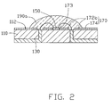
- FIG. 1 is a schematic, cross-sectional view of a light-emitting diode in accordance with a first embodiment, including an LED chip mounted on a reflective surface, and a hemispherical shaped encapsulation.
- FIG. 2 is similar to FIG.1 but with a different placement of the LED chip.
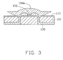
- FIG. 3 is similar to FIG. 1 but with a cone-shaped encapsulation.
- FIG. 4 is a schematic, cross-sectional view of a light-emitting diode in accordance with a second embodiment, including a blind via covered by an encapsulation.
- FIG. 5 is similar to FIG. 4 but with the blind via located inside of the encapsulation.
- the LED 100 includes a silicon substrate 110, an LED chip 150, and a light pervious encapsulation 190a.
- the silicon substrate 110 is configured for supporting the LED chip 150 and the encapsulation 190a thereon, and for dissipating heat generated from the LED chip 150.
- the silicon substrate 110 includes a surface 112.
- the surface 112 can be a flat surface.
- a plurality of electrodes 130 extends through the silicon substrate 110 and is made of an electrically conductive material.
- the electrically conductive material can be an electrically conductive paste or a metal, such as gold, silver, aluminum and etc.
- each of the electrodes 130 has an L shaped cross section.
- the LED chip 150 is mounted on the surface 112 of the silicon substrate 110.
- the silicon substrate 110 dissipates the heat generated by the LED chip 150 towards the outside of the LED 10.
- the LED chip 150 can be electrically connected with the electrode 130 by a wiring bonding technique.
- a reflective layer 170 is formed on the surface 112 of the silicon substrate 110 for reflecting light emitted from the LED chip 150 toward the encapsulation 190a.
- the reflective layer 170 includes a first reflective portion 172a and a second reflective portion 174.
- the first reflective portion 172a and the second reflective portion 174 are coplanar and formed on the surface 112 of the substrate 110.
- the first reflective portion 172a is sandwiched between the LED chip 150 and the surface 112.
- the LED chip 150 can be adhesively mounted on the first reflective portion 172a by silver ink.
- the reflective layer 170 can be made of a reflective material.
- the reflective material can be a metal such as silver, aluminum, copper and etc.
- the reflective material also can be ceramic powder or TiO2.
- the first reflective layer and the second reflective layer can be insulated with all of the electrodes 130 or at least one of the electrodes 130.
- a through hole 173 can be defined in the middle of the first reflective portion 172b.
- the LED chip 150 in the through hole 173 can be mounted directly on the surface 112 of the silicon substrate 110.
- the height of the first reflective portion 172b is smaller than that of the LED chip 150.
- the encapsulation 190a is disposed on the surface 112 of the substrate and covers the LED chip 150, the first reflective portion 172a and a portion of the second reflective portion 174.
- the encapsulation 190a is configured for converging a direction of the light emitted from the LED chip 150, thus adjusting an illuminating scope of the LED 100.
- the encapsulation 190a protects the LED chip 150 from contaminants.
- a refractive index of the encapsulation 190a is, for example, in an approximate range of 1.4 to 1.55.
- the encapsulation 190a can be made of a light-permeable material including but not limited to cyclic olefin copolymer (COC), polymethylmethacrolate (PMMA), polycarbonate (PC), PC and/or PMMA, and polyetherimide (PIE).
- COC cyclic olefin copolymer
- PMMA polymethylmethacrolate
- PC polycarbonate
- PIE polyetherimide
- the encapsulation 190a can be hemisphere-shaped.
- the encapsulation 190a also can be other shapes known in the art having light gathering function, such as a cone-shaped lens 190b having an aspheric surface, referring to FIG. 3 .
- an LED 200 according to a second embodiment is shown.
- the structure of the LED 200 is similar with that of the LED 100 in the first embodiment.
- the LED 200 includes a silicon substrate 210, an LED chip 150, and a light pervious encapsulation 190a.
- the difference is that a blind via 214 is defined in the surface 212 of the substrate 210.
- the blind via 214 is exposed to the outside of the encapsulation 190a.
- An auxiliary electric component 220 is completely received in the blind via 214 positioned below the surface 112 of the silicon substrate 110.
- the auxiliary electric component 220 does not absorb/block light emitted from the LED chip 150. All the light emitted from the LED chip 150 can reach the encapsulation 190a. As a result, the brightness and the luminous efficiency of the LED 200 are stably maintained.
- the auxiliary electric component 220 is an anti-static electric component, such as a zener diode, a Schottky barrier diode (SND), a silicon-based tunneling diode, an integrated circuit for static electricity protection and etc.
- the auxiliary electric component 220 is electrically connected with the LED chip 150 in parallel (not shown) so that the auxiliary electric component 220 prevents the LED chip 150 from reverse breakdown caused by static electricity.
- the auxiliary electric component 320 can be a light intensity sensor.
- the blind via 214 is defined in the surface 112 of the substrate 210 and inside the coverage of the encapsulation 190a, so that the auxiliary electric component 320 can precisely measure the light intensity of the LED chip 150.
- the light intensity sensor may be connected with a feedback circuit (not shown) for stabilizing the intensity of the LED chip 150.
- the reflective layer 170 can be replaced by a fluorescent layer made of fluorescent materials.
- the fluorescent layer is configured for providing light of a desirable color.
Landscapes
- Led Device Packages (AREA)
Applications Claiming Priority (1)
| Application Number | Priority Date | Filing Date | Title |
|---|---|---|---|
| CN2007102029837A CN101459211B (zh) | 2007-12-11 | 2007-12-11 | 固态发光器件 |
Publications (1)
| Publication Number | Publication Date |
|---|---|
| EP2071637A2 true EP2071637A2 (de) | 2009-06-17 |
Family
ID=40329088
Family Applications (1)
| Application Number | Title | Priority Date | Filing Date |
|---|---|---|---|
| EP08253440A Withdrawn EP2071637A2 (de) | 2007-12-11 | 2008-10-22 | Lichtemittierende Diode |
Country Status (3)
| Country | Link |
|---|---|
| US (1) | US7994518B2 (de) |
| EP (1) | EP2071637A2 (de) |
| CN (1) | CN101459211B (de) |
Cited By (1)
| Publication number | Priority date | Publication date | Assignee | Title |
|---|---|---|---|---|
| EP2556293A4 (de) * | 2010-04-07 | 2014-05-21 | Appotronics Corp Ltd | Beleuchtungsvorrichtung von hoher helligkeit mit doppelseitiger ansteuerung von wellenlängenumwandlungsmaterialien |
Families Citing this family (40)
| Publication number | Priority date | Publication date | Assignee | Title |
|---|---|---|---|---|
| TWI426206B (zh) * | 2008-12-25 | 2014-02-11 | 友達光電股份有限公司 | 發光二極體裝置 |
| KR101064026B1 (ko) * | 2009-02-17 | 2011-09-08 | 엘지이노텍 주식회사 | 발광 디바이스 패키지 및 그 제조방법 |
| JP5343831B2 (ja) | 2009-04-16 | 2013-11-13 | 日亜化学工業株式会社 | 発光装置 |
| TWI472067B (zh) * | 2010-04-28 | 2015-02-01 | Lg伊諾特股份有限公司 | 光學封裝及其製造方法 |
| KR101130137B1 (ko) * | 2010-07-02 | 2012-03-28 | 연세대학교 산학협력단 | 발광다이오드 모듈 |
| TWI478319B (zh) * | 2010-07-20 | 2015-03-21 | 晶元光電股份有限公司 | 整合式發光裝置及其製造方法 |
| USD712850S1 (en) | 2010-11-18 | 2014-09-09 | Cree, Inc. | Light emitter device |
| USD721339S1 (en) | 2010-12-03 | 2015-01-20 | Cree, Inc. | Light emitter device |
| US8564000B2 (en) | 2010-11-22 | 2013-10-22 | Cree, Inc. | Light emitting devices for light emitting diodes (LEDs) |
| USD707192S1 (en) | 2010-11-18 | 2014-06-17 | Cree, Inc. | Light emitting device |
| CN102468406B (zh) * | 2010-11-19 | 2014-11-05 | 展晶科技(深圳)有限公司 | 发光二极管封装结构及其制造方法 |
| US9490235B2 (en) | 2010-11-22 | 2016-11-08 | Cree, Inc. | Light emitting devices, systems, and methods |
| US9300062B2 (en) | 2010-11-22 | 2016-03-29 | Cree, Inc. | Attachment devices and methods for light emitting devices |
| US9000470B2 (en) | 2010-11-22 | 2015-04-07 | Cree, Inc. | Light emitter devices |
| US8575639B2 (en) | 2011-02-16 | 2013-11-05 | Cree, Inc. | Light emitting devices for light emitting diodes (LEDs) |
| US8624271B2 (en) | 2010-11-22 | 2014-01-07 | Cree, Inc. | Light emitting devices |
| CN102479909B (zh) * | 2010-11-24 | 2014-12-10 | 展晶科技(深圳)有限公司 | 发光二极管 |
| USD706231S1 (en) | 2010-12-03 | 2014-06-03 | Cree, Inc. | Light emitting device |
| USD702653S1 (en) | 2011-10-26 | 2014-04-15 | Cree, Inc. | Light emitting device component |
| US8809880B2 (en) | 2011-02-16 | 2014-08-19 | Cree, Inc. | Light emitting diode (LED) chips and devices for providing failure mitigation in LED arrays |
| US8455908B2 (en) * | 2011-02-16 | 2013-06-04 | Cree, Inc. | Light emitting devices |
| TWI517452B (zh) * | 2011-03-02 | 2016-01-11 | 建準電機工業股份有限公司 | 發光晶體之多晶封裝結構 |
| USD705181S1 (en) | 2011-10-26 | 2014-05-20 | Cree, Inc. | Light emitting device component |
| CN104081112B (zh) | 2011-11-07 | 2016-03-16 | 克利公司 | 高电压阵列发光二极管(led)器件、设备和方法 |
| US9735198B2 (en) | 2012-03-30 | 2017-08-15 | Cree, Inc. | Substrate based light emitter devices, components, and related methods |
| US10134961B2 (en) | 2012-03-30 | 2018-11-20 | Cree, Inc. | Submount based surface mount device (SMD) light emitter components and methods |
| CN103000785A (zh) * | 2012-11-05 | 2013-03-27 | 何忠亮 | 一种led发光结构及其制作方法 |
| US9345091B2 (en) | 2013-02-08 | 2016-05-17 | Cree, Inc. | Light emitting device (LED) light fixture control systems and related methods |
| US10295124B2 (en) * | 2013-02-27 | 2019-05-21 | Cree, Inc. | Light emitter packages and methods |
| DE102013215326A1 (de) * | 2013-04-30 | 2014-10-30 | Tridonic Jennersdorf Gmbh | LED-Modul mit hochreflektierender Fläche |
| USD739565S1 (en) | 2013-06-27 | 2015-09-22 | Cree, Inc. | Light emitter unit |
| USD740453S1 (en) | 2013-06-27 | 2015-10-06 | Cree, Inc. | Light emitter unit |
| CN104282830B (zh) * | 2013-07-12 | 2018-01-30 | 展晶科技(深圳)有限公司 | 发光二极管模组 |
| JP6201617B2 (ja) * | 2013-10-17 | 2017-09-27 | 日亜化学工業株式会社 | 発光装置 |
| CN104393159A (zh) * | 2014-10-21 | 2015-03-04 | 深圳市瑞丰光电子股份有限公司 | 一种led灯丝 |
| CN111509110A (zh) * | 2014-11-18 | 2020-08-07 | 首尔半导体株式会社 | 发光装置 |
| US9252337B1 (en) | 2014-12-22 | 2016-02-02 | Bridgelux, Inc. | Composite substrate for light emitting diodes |
| USD823492S1 (en) | 2016-10-04 | 2018-07-17 | Cree, Inc. | Light emitting device |
| CN118712309A (zh) * | 2020-11-20 | 2024-09-27 | 隆达电子股份有限公司 | 发光装置、背光板及显示面板 |
| JP2024118546A (ja) * | 2023-02-21 | 2024-09-02 | シャープディスプレイテクノロジー株式会社 | 照明装置、表示装置及び照明装置の製造方法 |
Family Cites Families (11)
| Publication number | Priority date | Publication date | Assignee | Title |
|---|---|---|---|---|
| JP2735089B2 (ja) | 1993-03-22 | 1998-04-02 | 株式会社サトミ製作所 | 軽質の細かい異物の除去方法 |
| CN1129968C (zh) * | 2000-11-23 | 2003-12-03 | 诠兴开发科技股份有限公司 | 发光二极管的封装方法 |
| KR200299491Y1 (ko) * | 2002-09-02 | 2003-01-03 | 코리아옵토 주식회사 | 표면실장형 발광다이오드 |
| TWM246811U (en) | 2003-07-28 | 2004-10-11 | Lightop Technology Co Ltd | Improved light emitting diode structure with fluorescent ink |
| US8610145B2 (en) * | 2003-09-30 | 2013-12-17 | Kabushiki Kaisha Toshiba | Light emitting device |
| US7329905B2 (en) * | 2004-06-30 | 2008-02-12 | Cree, Inc. | Chip-scale methods for packaging light emitting devices and chip-scale packaged light emitting devices |
| TWI249257B (en) | 2004-09-24 | 2006-02-11 | Epistar Corp | Illumination apparatus |
| JP4176703B2 (ja) * | 2004-11-25 | 2008-11-05 | 松下電器産業株式会社 | 半導体発光装置、照明装置、携帯通信機器、カメラ、及び製造方法 |
| TW200721525A (en) | 2005-11-16 | 2007-06-01 | High Power Lighting Corp | Package structure of combining zener diode chip and light-emitting diode chip |
| US7607815B2 (en) * | 2006-11-27 | 2009-10-27 | Avago Technologies Ecbu Ip (Singapore) Pte. Ltd. | Low profile and high efficiency lighting device for backlighting applications |
| US20080246397A1 (en) * | 2007-04-04 | 2008-10-09 | Bily Wang | Manufacturing method of white light led and structure thereof |
-
2007
- 2007-12-11 CN CN2007102029837A patent/CN101459211B/zh not_active Expired - Fee Related
-
2008
- 2008-09-02 US US12/202,555 patent/US7994518B2/en not_active Expired - Fee Related
- 2008-10-22 EP EP08253440A patent/EP2071637A2/de not_active Withdrawn
Cited By (1)
| Publication number | Priority date | Publication date | Assignee | Title |
|---|---|---|---|---|
| EP2556293A4 (de) * | 2010-04-07 | 2014-05-21 | Appotronics Corp Ltd | Beleuchtungsvorrichtung von hoher helligkeit mit doppelseitiger ansteuerung von wellenlängenumwandlungsmaterialien |
Also Published As
| Publication number | Publication date |
|---|---|
| CN101459211A (zh) | 2009-06-17 |
| CN101459211B (zh) | 2011-03-02 |
| US7994518B2 (en) | 2011-08-09 |
| US20090146155A1 (en) | 2009-06-11 |
Similar Documents
| Publication | Publication Date | Title |
|---|---|---|
| EP2071637A2 (de) | Lichtemittierende Diode | |
| CN101315963B (zh) | 半导体发光装置 | |
| CN101371358B (zh) | 具有集成静电放电保护的用于发光二极管的封装 | |
| US10043954B2 (en) | Lighting device with a phosphor layer on a peripheral side surface of a light-emitting element and a reflecting layer on an upper surface of the light-emitting element and on an upper surface of the phosphor layer | |
| JP5746076B2 (ja) | 半導体発光デバイスパッケージのサブマウント及びそのサブマウントを備える半導体発光デバイスパッケージ | |
| US10355183B2 (en) | LED package | |
| EP2398072A1 (de) | Lichtemittierendes halbleiterbauelement | |
| US8368085B2 (en) | Semiconductor package | |
| US8569789B2 (en) | Light emitting diode package with reflective layer | |
| US10559728B2 (en) | Semiconductor package structure | |
| US20130009183A1 (en) | Reflective circuit board for led backlight | |
| JP5955318B2 (ja) | 発光ダイオード | |
| JP6738224B2 (ja) | Ledパッケージ | |
| CN102939670A (zh) | 光电子器件 | |
| US8461599B2 (en) | Light emitting diode with a stable color temperature | |
| US20120138962A1 (en) | Light emitting diode package | |
| EP2360993A2 (de) | Lichtemittierende Vorrichtung mit Rauschunterdrückung und Beleuchtungsvorrichtung beinhaltend dieselbe | |
| CN105720180B (zh) | Led模块 | |
| US20140001500A1 (en) | Led light bar | |
| US20090159913A1 (en) | Light-emitting diode | |
| CN104518075B (zh) | 发光二极管封装结构 | |
| KR20110138756A (ko) | 발광 소자 | |
| KR101610384B1 (ko) | 발광 소자 및 이를 이용한 발광 모듈 | |
| US10978628B2 (en) | Device and connection carrier | |
| US10510931B2 (en) | Side-view light emitting diode package structure |
Legal Events
| Date | Code | Title | Description |
|---|---|---|---|
| PUAI | Public reference made under article 153(3) epc to a published international application that has entered the european phase |
Free format text: ORIGINAL CODE: 0009012 |
|
| AK | Designated contracting states |
Kind code of ref document: A2 Designated state(s): AT BE BG CH CY CZ DE DK EE ES FI FR GB GR HR HU IE IS IT LI LT LU LV MC MT NL NO PL PT RO SE SI SK TR |
|
| AX | Request for extension of the european patent |
Extension state: AL BA MK RS |
|
| STAA | Information on the status of an ep patent application or granted ep patent |
Free format text: STATUS: THE APPLICATION IS DEEMED TO BE WITHDRAWN |
|
| 18D | Application deemed to be withdrawn |
Effective date: 20110503 |