EP2069721B1 - Chopped hall effect sensor - Google Patents
Chopped hall effect sensor Download PDFInfo
- Publication number
- EP2069721B1 EP2069721B1 EP07796403.9A EP07796403A EP2069721B1 EP 2069721 B1 EP2069721 B1 EP 2069721B1 EP 07796403 A EP07796403 A EP 07796403A EP 2069721 B1 EP2069721 B1 EP 2069721B1
- Authority
- EP
- European Patent Office
- Prior art keywords
- output
- filter
- signal
- hall
- input
- Prior art date
- Legal status (The legal status is an assumption and is not a legal conclusion. Google has not performed a legal analysis and makes no representation as to the accuracy of the status listed.)
- Active
Links
- 230000005355 Hall effect Effects 0.000 title claims description 52
- 230000004044 response Effects 0.000 claims description 31
- 238000012935 Averaging Methods 0.000 claims description 14
- 238000001914 filtration Methods 0.000 claims description 6
- 238000005070 sampling Methods 0.000 description 17
- 238000000034 method Methods 0.000 description 10
- 238000009499 grossing Methods 0.000 description 8
- 230000008901 benefit Effects 0.000 description 5
- 238000012546 transfer Methods 0.000 description 5
- 238000010586 diagram Methods 0.000 description 4
- 238000013461 design Methods 0.000 description 3
- 230000002411 adverse Effects 0.000 description 2
- 230000002238 attenuated effect Effects 0.000 description 2
- 230000000295 complement effect Effects 0.000 description 2
- 230000008878 coupling Effects 0.000 description 2
- 238000010168 coupling process Methods 0.000 description 2
- 238000005859 coupling reaction Methods 0.000 description 2
- 230000000694 effects Effects 0.000 description 2
- 230000008569 process Effects 0.000 description 2
- 238000012545 processing Methods 0.000 description 2
- 230000006641 stabilisation Effects 0.000 description 2
- 238000011105 stabilization Methods 0.000 description 2
- 230000007704 transition Effects 0.000 description 2
- 238000009825 accumulation Methods 0.000 description 1
- 230000003321 amplification Effects 0.000 description 1
- 239000003990 capacitor Substances 0.000 description 1
- 230000008859 change Effects 0.000 description 1
- 230000003116 impacting effect Effects 0.000 description 1
- 230000007246 mechanism Effects 0.000 description 1
- 238000003199 nucleic acid amplification method Methods 0.000 description 1
- 230000010363 phase shift Effects 0.000 description 1
- 238000011084 recovery Methods 0.000 description 1
- 239000004065 semiconductor Substances 0.000 description 1
- 230000035945 sensitivity Effects 0.000 description 1
- 238000009987 spinning Methods 0.000 description 1
- 230000001360 synchronised effect Effects 0.000 description 1
- 238000009966 trimming Methods 0.000 description 1
Images


Classifications
-
- G—PHYSICS
- G01—MEASURING; TESTING
- G01D—MEASURING NOT SPECIALLY ADAPTED FOR A SPECIFIC VARIABLE; ARRANGEMENTS FOR MEASURING TWO OR MORE VARIABLES NOT COVERED IN A SINGLE OTHER SUBCLASS; TARIFF METERING APPARATUS; MEASURING OR TESTING NOT OTHERWISE PROVIDED FOR
- G01D3/00—Indicating or recording apparatus with provision for the special purposes referred to in the subgroups
- G01D3/02—Indicating or recording apparatus with provision for the special purposes referred to in the subgroups with provision for altering or correcting the law of variation
-
- G—PHYSICS
- G01—MEASURING; TESTING
- G01R—MEASURING ELECTRIC VARIABLES; MEASURING MAGNETIC VARIABLES
- G01R33/00—Arrangements or instruments for measuring magnetic variables
- G01R33/02—Measuring direction or magnitude of magnetic fields or magnetic flux
-
- G—PHYSICS
- G01—MEASURING; TESTING
- G01R—MEASURING ELECTRIC VARIABLES; MEASURING MAGNETIC VARIABLES
- G01R33/00—Arrangements or instruments for measuring magnetic variables
- G01R33/02—Measuring direction or magnitude of magnetic fields or magnetic flux
- G01R33/06—Measuring direction or magnitude of magnetic fields or magnetic flux using galvano-magnetic devices
- G01R33/07—Hall effect devices
-
- G—PHYSICS
- G06—COMPUTING; CALCULATING OR COUNTING
- G06M—COUNTING MECHANISMS; COUNTING OF OBJECTS NOT OTHERWISE PROVIDED FOR
- G06M1/00—Design features of general application
- G06M1/27—Design features of general application for representing the result of count in the form of electric signals, e.g. by sensing markings on the counter drum
- G06M1/274—Design features of general application for representing the result of count in the form of electric signals, e.g. by sensing markings on the counter drum using magnetic means; using Hall-effect devices
Definitions
- This invention relates generally to Hall effet sensors and, more particularly, to a chopped Hall effect sensor having fast response time and reduced noise.
- Hall effect sensors are used in a wide variety of applications including industrial and consumer applications. As one example, Hall effect sensors are widely used in the automotive industry for mechanical position sensing, such as gear tooth sensors used in brake systems. Such applications require accuracy.
- Hall effect elements or plates experience imbalances due to resistance gradients, geometrical asymmetries and piezoresistive effects which can introduce an offset voltage.
- the magnitude and polarity of the offset voltage are a function of stresses in the semiconductor from which the element is formed, which stresses vary with mechanical pressure and temperature.
- Various techniques have been used to address and cancel the Hall offset voltage, including chopper stabilization techniques.
- the autozero technique involves sampling the offset, follower by subtraction of this sampled offset from the input signal, which is then amplified.
- the chopper technique involves the use of filtering, modulation and demodulation. Topically, modulation is performed on the input signal, which is then combined with the unmodulated offset signal prior to amplification and subsequent demodulation. This demodulation has the effect of demodulating the modulated input signal and modulating the unmodulated offset signal. This modulated offset signal is then filtered out using a low pass filter.
- the switched Hall plate sometimes referred to alternatively as a spinning Hall plate, includes a Hall element having (typically) for contacts and a modulation switch circuit to periodically connect the supply voltage and the amplifier input to one pair of contacts or the other. Quadrature phases of operation are defined by complimentary clock signals.
- Use of such a switched Hall plate provides a way to discriminate the Hall offset voltage (referred to herein as the Hall offset signal component) from the magnetically induced signals (referred to herein as the magnetic signal component). In one such circuit, the switched Hall plate modulates the magnetic signal component and the offset signal component remains substantially invariant.
- the chopped amplifier demodulates the magnetic signal component and modulates the offset signal component which is then attenuated by the low pass filter to provide the sensor output signals. While this technique is effective to remove the Hall offset voltage the resulting ripple on the sensor output signal and the sensor response time must be balanced since, the more filtering applied, the lower the resulting ripple, but also the slower the sensor response time.
- Hall effect sensor applications additionally require faster response times to input magnetic field steps.
- Hall effect sensors used in current sensing applications must respond quickly to step changes in the magnetic field, for example in order to rapidly detect fault conditions, such as short circuits in automobile batteries.
- this circuit entirely eliminates ripple on the sensor output signal and thus, provides a faster step response time by avoiding ripple filtering; however, these benefits are achieved at the cost of a degraded signal to noise ratio. This is because the sampling and holding operation can produce noise fold back (i.e., aliasing) since the baseband noise is undersampled.
- a Hall effect sensor includes a Hall element, a Hall plate modulation circuit, an amplifier, and a filter including a selective filter tuned to the modulation frequency.
- the Hall plate modulation circuit is responsive to the output signal of the Hall element and operates to modulate the magnetic signal component or the offset signal component of the Hall output signal.
- the amplifier is responsive to the modulation circuit output signal and provides an amplifier output signal to the filter.
- the filter includes an anti-aliasing filter coupled between the amplifier and the selective filter.
- the Hall effect sensor is provided with fast response time through the use of the selective filter that removes the offset signal component with its associated ripple, thereby eliminating the significant low pass filtering requirements of some conventional chopped Hall effect sensors.
- a high signal to noise ratio is achieved with the use of the anti-aliasing filter that removes frequency components above a predetermined frequency, so that the selective filter meets the Nyquist criterion for noise signals, thereby reducing baseband noise by preventing aliasing.
- the offset signal component is modulated by the modulation circuit
- an even number of additional modulation circuits are provided between the output of the Hall plate modulation circuit and the input to the filter. In this way, the offset signal component is modulated when it reaches the selective filter for removal.
- the amplifier includes an odd number of additional modulation circuits between the output of the Hall plate modulation circuit and the input to the filter, again ensuring that the offset signal component is modulated when it reaches the selective filter for removal.
- Embodiments of the invention may include one or more of the following features.
- the amplifier may be a closed or open loop amplifier.
- the loop may be closed at the input to the anti-aliasing filter, at the output of the anti-aliasing filter, or at the output of the selective filter.
- the anti-aliasing filter may serve an additional loop compensation purpose.
- the filter may include a smoothing filter.
- the amplifier may or may not be chopped.
- the amplifer must be chopped.
- the feedback network may or may not be chopped.
- One illustrative selective filter includes a plurality of sample and hold circuits arranged in pairs, with each sample and hold circuit having an input coupled to the output of the anti-aliasing filter and an output.
- the filter further includes an averaging circuit having a plurality of inputs, each coupled to the output of a respective sample and hold circuit, and an output at which the selective filter output signal is provided.
- Each of the sample and hold circuits samples the input signal at the modulation frequency and at a phase separated from the phase of the other sample and hold circuit of the same pair by 180 degrees and at a phase arbitrarily separated from the phase at which the other pairs of sample and hold circuits operate.
- the anti-aliasing filter includes a first sample and hold circuit having an input coupled to the output of the anti-aliasing filter, a second sample and hold circuit having an input coupled to the output of the anti-aliasing filter, and an averaging circuit having inputs coupled to the outputs of the first and second sample and hold circuits.
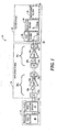
- a chopped Hall effect sensor 10 includes a switched Hall plate 14 providing a switched Hall output signal 16, an amplifier stage 24 having an input responsive to the switched Hall output signal 16 and an output at which is provided an amplifier output signal 26, and a filter stage 34 having an input responsive to the amplifier output signal 26 and an output at which is provided a sensor output signal 36.
- the filter stage 34 includes an anti-aliasing filter 38 and a selective filter 40, as shown.
- the Hall effect sensor 10 is provided with low noise and fast response time.
- Fast response time is achieved with the use of the selective filter 40 that removes the offset signal component with its associated ripple, thereby eliminating the significant low pass filtering requirements of some conventional chopped Hall effect sensors.
- a high signal to noise ratio is achieved with the use of the anti-aliasing filter 38 to remove frequency components above a predetermined frequency, so that the selective filter 40 meets the Nyquist criterion for noise signals, thereby reducing resulting baseband noise by preventing aliasing.
- the anti-aliasing filter 38 removes frequency components above the sensor clock frequency and the selective filter 40 samples at twice the clock frequency.
- the anti-aliasing filter is a low pass filter.
- the filter requirements of the anti-aliasing filter are relaxed as compared to conventional chopped Hall sensors in which the low pass filter is the mechanism for removing the offset signal component with its associated ripple.
- the anti-aliasing filter 38 is a first order low pass filter.
- the switched Hall plate 14 includes a Hall element or plate 18 having an output at which is provided a Hall output signal 20 that varies in accordance with a sensed magnetic field and a Hall plate modulation switch circuit, or simply a Hall plate modulation circuit 22 having an input responsive to the Hall output signal and an output at which is provided the switched Hall output signal (also referred to herein as the modulation circuit output signal) 16.
- the switched Hall output signal 16 is coupled to an input of the amplifer stage 24, as shown.
- the Hall output signal 20 and switched Hall output signal 16 include a magnetic signal component V H and a Hall offset signal component V op .
- the modulation circuit 22 may be controlled to modulate the Hall offset signal component V op or the magnetic signal component V H at a modulation frequency, referred to alternatively herein as the clock frequency f CLK .
- a modulation frequency referred to alternatively herein as the clock frequency f CLK .
- An illustrative, conventional modulation circuit that modulates the Hall offset signal component V op is shown and described in connection with Figures 2-2C and an illustrative, conventional modulation circuit that modulates the magnetic signal component V H is shown and described in connection with Figures 3-3C .
- the Hall effect sensor 10 includes an even number of modulation circuits between the output of the Hall plate modulation circuit 22 and the input of the filter stage 34 in order to enable the selective filter 40 to remove the modulated offset signal component.
- One illustrative Hall effect sensor of this type is shown in Figure 4 .
- the even number of modulation circuits in the amplifier stage operate to, one or more times, demodulate and again modulate the offset Signal component to ensure that the offset signal component is modulated when it reaches the filter stage and thus, can be removed by the selective filter 40 in order to recover the magnetic signal component.
- the amplifer stage 24 may not be a chopped amplifier and thus, may not perform any signal modulation, thereby resulting in zero modulation circuits between the output of the Hall plate modulation circuit 22 and the input to the filter stage 34.
- the Hall effect sensor 10 includes an odd number of modulation circuits between the output of the Hall plate modulation circuit 22 and the input of the filter stage 34 in order to enable the selective filter 40 to remove the offset signal component.
- One illustrative Hall effect sensor of this type is shown in Figure 5 . With this arrangement, the odd number of modulation circuits in the amplifier stage ensures that the offset signal component is modulated when it reaches the filter stage and thus, can be removed by the selective filter 40 in order to recover the magnetic signal component.
- At least one amplifier 30a - 30n comprising the amplifer stage 24 is a chopped amplifier in embodiments in which the modulation circuit 22 modulates the magnetic signal component since otherwise, the offset signal component would not be up-converted for removal by the selective filter (and optionally more than one amplifier 30a - 30n is chopped, as long as an odd number of chopper stages are used).
- the amplifer stage 24 may include one or more amplifiers 30a - 30n.
- Each amplifier 30a - 30n has a gain stage 32a - 32n and may or may not be chopped. If chopped, the amplifier includes at least one modulation circuit, as may be provided by a pair of cross-coupled switches 46a - 46n and may additionally include a second modulation circuit, as may be provided by a pair of cross-coupled switches 42a - 42n, as shown in dotted lines for amplifier 30a and in solid lines for amplifier 30n.
- Each of the amplifiers 30a - 30n like the Hall element 18, has an associated offset voltage, here shown by respective voltage sources 48a - 48n at the input to the respective gain stage 32a - 32n.
- the modulation circuits 42a - 42n and 46a 46n operate to modulate or demodulated the processed signal and may be implemented, for example with MOSFET switches. In the illustrated embodiment, the modulation circuits 42a - 42n and 46a - 46n operate at the clock frequency f CLK . It will be appreciated however that the amplifier stage 24 may be chopped at a different frequency than the clock frequency used by the Hall plate modulation circuit 22.
- the particular choice of number of amplifiers 30a - 30n comprising the amplifier stage 24 is based generally on the desired overall gain for the amplifier 24. It is desirable that the amplifier gain be large enough so that any offset associated with any non-chopped circuitry that follows the filter stage 34 is signifcantly less than the Hall and amplifier offsets, thereby minimizing the contribution of such "back-end" offset.
- the overall gain is selected, how much gain is provided by any given amplifier 30a - 30n requires consideration of various factors such as bandwidth and response time. For example, in closed loop configurations, the higher the gain for a particular stage, the lower the bandwidth; however, the lower the bandwidth, the slower the sensor response time.
- each amplifier need not be identical in terms of topology and specifications.
- the gain of the different amplifiers 30a - 30n may vary.
- the topologies may vary.
- the amplifiers 30a - 30n may be closed or open loop amplifiers.
- Whether one or more of the amplifiers 30a - 30n includes one or two modulation circuits 42a - 42n, 46a - 46n is based on whether the Hall plate modulation circuit 22 modulates the Hall offset signal component V op or the magnetic signal component V H , since as mentioned above, in the former case, an even number of modulation circuits is required between the output of the Hall plate modulation circuit 22 and the input of the filter stage 34 in order to cancel the offset signal component and in the latter case, an odd number of modulation circuits is required between the output of the Hall plate modulation circuit and the input of the filter stage in order to cancel the offset signal component.
- the anti-aliasing filter 38 removes frequency components as necessary to ensure that the selective filter 40 meets the Nyquist criterion for noise signals.
- the filter 38 has a cutoff frequency on the order of 0.35f CLK .
- various filter designs are possible for the low pass filter and the particular cutoff frequency of the filter 38 is a function of the sampling frequency of the selective filter 40 and the desired sensor response time.
- the selective filter 40 is tuned to a frequency at which incoming signals are eliminated and also attenuates other frequency components above a given bandwidth.
- the selective filter 40 is tuned to a frequency selected to ensure removal of the offset signal component with its associated ripple.
- the selective filter is tuned to the clock frequency f CLK at which the offset signal component is modulated when it reaches the selective filter.
- the selective filter 40 is a sampled data filter in the form of a sine filter having a frequency domain transfer function shaped like a sinc function (see Figure 7A ) and a time domain transfer function shaped like a rectangular function.
- the selective filter 40 is a discrete time filter in the sense that its zeros in the frequency domain are at exactly the harmonics related to one-half of the sample frequency.
- the selective filter samples at a frequency equal to twice the sensor clock frequency f CLK .
- the zeros are located at N(f SF /2) or Nf CLK , where N is any integer.
- the filter 40 removes all the signal components at the clock frequency f CLK and its harmonics and attenuates the other frequency components above a given bandwidth.
- the selective filter eliminates the undesired output ripple, whose amplitude is proportional to the DC input offset signal component.
- the resulting sensor output signal 36 includes only the magnetic signal component, since the selective filter entirely eliminates the offset signal component with its associated ripple.
- the extent of attenuation at frequencies other than harmonics of the clock frequency is a function of the number of samples of the input signal taken within one clock period, with greater attenuation achieved by taking more samples.
- the particular selection of the sample frequency requires a tradeoff between greater signal attenuation as is achieved by averaging a larger number of samples (as will provide a higher overall sampling frequency) versus area efficiency achieved by using the minimum number of samples (as will provide a lower overall sampling frequency).
- the illustrative selective filter 40 is a sample based sinc filter
- alternative filter designs are possible while still achieving the benefits of the illustrative selective filter; namely, of eliminating the offset signal component with its associated ripple.
- the selective filter 40 is an averaging filter and may take the form of a continuous time filter, discrete timefilter, an analog filter, or a digital filter. As one example, a continuous time comb filter may be used.
- the filter stage 34 may include an optional smoothing filter 44 to further attenuate high frequency content (not located at the clock harmonics) in addition to the attenuation already supplied by the selective filter 40. Additionally, since this smoothing filter 44 is only intended for high frequency attenuation (secondary side lobes of the selective filter transfer function), its cutoff frequency does not need to be small. For example, in the illustrative embodiment, the smoothing filter has a cutoff frequency of at least f CLK . Thus, the smoothing filter 44 does not introduce any significant delay to the sensor.
- a conventional switched Hall plate 50 of the type that modulates the Hall offset signal component is shown to include a Hall element or plate 52 and a Hall plate modulation switch circuit 54.
- the Hall element 52 includes four equally spaced contacts 52a, 52b, 52c, and 52d, each coupled to a first terminal of a respective switch 56a, 56b, 56c, and 56d, as shown.
- a second terminal of switches 56b and 56c are coupled to provide the positive node of the switched Hall output signal 16, here labeled Vo+, and the second terminal of switches 56a and 56d are coupled to provide the negative node of the switched Hall output signal 16, here labeled Vo-.
- switches 60a, 60b, 60c, and 60d are arranged to selectively couple the Hall contacts 52a, 52b, 52c, 52d to the supply voltage Vs and ground. More particularly, switches 56b, 56d, 60a, and 60c are controlled by a clock signal CLK and switches 56a, 56c, 60b, and 60d are controlled by a complementary clock signal CLK/, as shown.
- the clock signals CLK and CLK/ have two states, a ⁇ 0 . state and a ⁇ 90 . state, as shown in Figure 2A .
- phase ⁇ 0* current flows from terminal 52a to 52c and the switched Hall output signal Vo is equal to V H + V op , where V op is the Hall plate offset voltage or Hall offset signal component and V H is the magnetic signal component.
- phase ⁇ 90* current flows from terminal 52b to 52d and the switched Hall output signal Vo is equal to V H - V op .
- the modulation switch circuit 54 modulates the Hall offset signal component V op , as shown in Figure 2B for zero Gauss.
- the magnetic signal component V H remains substantially invariant, as shown in Figure 2C .
- an alternative conventional switched Hall plate 70 of the type that modulates the magnetic signal component is shown to include a Hall element 72 and a Hall plate modulation switch circuit 74.
- the Hall element 72 is identical to element 52 of Figure 2 and includes four contacts 72a, 72b, 72c, and 72d, each coupled to a first terminal of a respective switch 76a, 76b, 76c, and 76d.
- a second terminal of switches 76a and 76b are coupled to provide the positive node of the switched Hall output signal, here labeled Vo+, and the second terminal of switches 56c and 56d are coupled to provide the negative node of the switched Hall output signal, here labeled Vo-.
- a comparison of Figures 2 and 3 reveals that the output contacts of the Hall element are interchanged during the ⁇ 90 - phase.
- Additional switches 80a, 80b, 80c, and 80d are arranged to selectively couple the Hall contacts 72a, 72b, 72c, and 72d to the supply voltage Vs and ground.
- Switches 76b, 76d, 80a, and 80c are controlled by clock signal CLK and switches 76a, 76c, 80b, and 80d are controlled by complementary clock signal CLK/, as shown.
- Clock signals CLK and CLK/ are identical to like signals in Figure 2 and thus have two states ⁇ 0* and ⁇ 90* , as shown.
- the modulation switch circuit 54 modulates the magnetic signal component to provide a modulated magnetic signal component V H , as shown in Figure 3C for zero Gauss.
- the Hall offset signal component V op remains substantially invariant as is shown in Figure 3B .
- the Hall offset voltage can be represented as a voltage source 58 between the Hall element 52 and the Hall plate modulation switch circuit 54.
- the Hall offset voltage 58 is added to the amplifier offset voltage 48a for example ( Figure 1 ) after being modulated by the Hall plate modulation circuit 54 ( Figure 2 ) and demodulated by the modulation circuit 42a (if the same clock frequency f CLK is used for the Hall element and the amplifier).
- the Hall offset voltage appears at the output of the switched Hall plate, as shown by voltage source 78.
- the Hall offset voltage 78 is indistinguishable from the amplifier offset voltage 48a for example in embodiments not including optional modulation circuit 42a ( Figure 1 ).
- the Hall offset voltage and the amplifier offset voltage will be simultaneously processed and cancelled by the sensor 10 of the present invention.
- a chopped Hall effect sensor 100 includes a switched Hall plate 50 of the type shown in Figure 2 that provides a switched Hall output signal 114 comprising a modulated Hall offset signal component V op and a substantially invariant magnetic signal component V H , as shown in Figure 4A . Also shown in dotted lines in Figure 4A is the substantially invariant magnetic signal component of the signal 114.
- the sensor 100 further includes a chopped amplifier 110 having an input coupled to the output of the switched Hall plate 50 and an output at which an amplified signal 116 is provided.
- a filter stage 120 like filter stage 34 of Figure 1 , has an input coupled to the output of the amplifier stage 110 and an output at which the sensor output signal 118 is provided.
- the filter stage 120 is shown without the optional smoothing filter (labeled 44 in Figure 1 ).
- the amplifier 110 is a closed loop amplifier having a feedback network 124, as shown.
- One illustrative embodiment of the feedback network 124 is shown and described in connection with Figure 6 .
- Use of a closed loop amplifier is desirable due to the resulting high linearity and gain stability over frequency, temperature, process and power supply levels.
- the magnetic signal component V H ( Figure 4A ) is at baseband, the tighter bandwidth required of the closed loop amplifier 110 does not adversely impact recovery of the magnetic signal component.
- An additional advantage to the closed loop amplifiers 110 in the embodiment of Figure 4 is the ability to provide a higher gain amplifier while maintaining the same gain bandwidth product, therefore reducing the closed loop bandwidth as much as might be necessary to achieve stability.
- the filter stage 34 may be significant area savings. For example, if a Miller compensation scheme is used, where the "reflected" capacitance sets the cutoff frequency, and the bandwidth is able to be set to achieve both loop stability and to allow the selective filter 150 to meet the Nyquist criteria, then the low pass filter 144 can perform the functionality of both the Miller stage and the anti-aliasing filter. Alternatively, if the bandwidth cannot be set to meet both the stability and anti-aliasing requirements, regardless of whether the compensation scheme includes a Miller stage, then a separate anti-aliasing filter must be provided and the feedback loop can be closed before the anti-aliasing filter.
- the switched Hall output signal 114 is coupled to an input of a summing node 126 and the feedback network 124 is also coupled to an input of the summing node 126, as shown.
- the summing node 126 may be a current or a voltage summing node.
- the output of the summing node 126 is coupled to a first modulation circuit, here shown in the form of a pair of cross-coupled switches 130 that modulate the incoming signal at the clock frequency f CLK .
- the output signal 132 of modulation circuit 130 thus contains a modulated magnetic signal component and a demodulated offset signal component, as shown in Figure 4B . Also shown in dotted lines in Figure 4B is the demodulated offset signal component 132a.
- the offset signal component of the signal 132 includes the Hall offset signal component V op (as represented by voltage source 58 in Figure 2 ) and the amplifier offset signal component V oa (as represented by voltage source 134 in Figure 4 ).
- the clock frequency f CLK is selected such that the clock period is in the order of one-half (or less) of the desired step response time (SRT).
- the desired step response time is on the order of 2.0 ⁇ s
- the clock frequency is on the order of 1 MHz.
- Gain stage 138 provides an amplified signal to a further modulation circuit, here shown in the form of a pair of cross-coupled switches 140, as shown.
- the gain stage 138 must have a bandwidth large enough to pass the modulated magnetic signal component.
- the gain stage bandwidth is at least five times the clock frequency f CLK .
- the tighter bandwidth required to implement the amplifier 110 in a closed loop form must be balanced with the minimum bandwidth necessary to pass the desired magnetic signal component. Since the modulated magnetic signal component does not go through the filter 144 or the Miller feedback stage 124, the closed loop bandwidth does not affect the modulated signal bandwidth. Only the amplifier's section through which the modulated magnetic signal component passes needs to have enough bandwidth to pass the desired magnetic signal component.
- Modulation circuit 140 operates at the clock frequency f CLK to provide the amplified signal 116 containing a demodulated magnetic signal component and a modulated offset signal component, as shown in Figure 4C . Also shown in dotted lines in Figure 4C is the demodulated magnetic signal component 116a. Note again that the offset being modulated by the modulation circuit 140 includes the Hall offset and the amplifier offset which are added at the output of the first modulation circuit 130.
- the amplified signal 116 is coupled to the filter stage 120 and more particularly, to the anti-aliasing, low pass filter 144, as shown.
- the purpose of the filter 144 is to perform an anti-aliasing function by removing frequency components that would fold-back to the baseband.
- the selective filter 150 samples at a frequency equal to twice the clock frequency f CLK .
- the cutoff frequency of the filter 144 must be limited to a maximum of the clock frequency f CLK and in one illustrative embodiment is on the order of 0.35f CLK .
- the low pass filter 144 provides the filtered signal 148 of Figure 4D that includes a partially attenuated modulated offset signal component and a demodulated magnetic signal component.
- the signal 148 contains successive alternating polarity exponential responses which is the chopped amplifier's residual ripple. The degree of attenuation of the ripple depends directly on the cutoff frequency of the filter 144. Also shown in dotted lines in Figure 4D is the demodulated magnetic signal component 148a.
- the time constant ⁇ of the filter 144 must be such that the rise time does not exceed one-half of the desired step response time (SRT).
- SRT step response time
- the selective filter 150 is a discrete time filter having zeros located at N(f SF /2), where N is any integer and f SF is the sampling frequency.
- the selective filter 150 is a time domain averaging filter with which the input signal 148 is averaged at the rate f CLK and the sampling frequency f SF is selected to be equal to two times the clock frequency f CLK .
- the resulting sensor output signal 118 is shown in Figure 4E to include only the magnetic signal component (identical to magnetic signal component 148a as provided at the output of the filter 144), since the selective filter entirely eliminates the offset signal component 148 with its associated ripple.
- this embodiment contains an even number of modulation circuits between the output of the Hall plate modulation circuit 50 that modulates the Hall offset signal component and the input to the filter stage 120.
- the modulation circuit output signal 114 is processed by two modulation circuits 130 and 140, before reaching the low pass filter 144.
- Modulation circuit 130 demodulates the offset signal component to baseband and modulation circuit 140 then up-converts the offset signal component so that the selective filter 150 can remove the offset and its associated ripple to thereby recover the desired magnetic signal component.
- an alternative Hall effect sensor 200 includes a switched Hall plate 70 of the type shown in Figure 3 that provides a switched Hall plate output signal 214 comprising a substantially invariant Hall offset signal component V op and a modulated magnetic signal component V H , as shown in Figure 5A . Also shown in dotted lines in Figure 5A is the substantially invariant Hall offset signal component V op .
- the sensor 200 further includes a chopped amplifer 210 having an input coupled to the output of the switched Hall plate 70 and an output at which an amplified signal 216 is provided.
- a filter stage 220 has an input coupled to the output of the amplifier stage 210 and an output at which the sensor output signal 218 is provided.
- the optional smoothing filter is not shown.
- the amplifier 210 is a closed loop amplifier having a feedback network 224, as shown.
- the illustrative feedback network shown in Figure 6 is suitable to provide the feedback network 224 in the embodiment of Figure 5 . It will be appreciated by those of ordinary skill in the art, that the same advantages described above in connection with the closed loop amplitier 110 of Figure 4 are realized in the sensor of Figure 5 (e.g., high linearity, gain stability, higher gain and area savings).
- the tighter bandwidth required to implement the amplifier 210 in a closed loop form must be balanced with the minimum bandwidth necessary to pass the desired magnetic signal component. Since the modulated magnetic signal component does not go through the filter 244 or the Miller feedback stage 224, the closed loop bandwidth does not affect the modulated signal bandwidth. Only the amplifier section through which the modulated magnetic signal component passes needs to have enough bandwidth to pass the desired magnetic signal component.
- a summing node 226 has inputs coupled to the feedback network 224 and an output coupled to a first modulation circuit, shown here in the form of a pair of cross-coupled switches 230 that modulate the incoming signal at the clock frequency f CLK .
- the output signal of modulation circuit 230 is coupled to an input of the gain stage 238.
- the switched Hall output signal 214 is also coupled to the input of the gain stage 238, as shown. Thus, in this embodiment, the switched Hall output signal 214 is not processed by the modulation circuit 230.
- a voltage source 234 representing the amplitier offset signal component V oa .
- Gain stage 238 provides an amplified signal to a further modulation circuit, here in the form of a pair of cross-coupled switches 240, as shown.
- the gain stage 238 must have a bandwidth large enough to pass the magnetic signal component that has been modulated by the switched Hall plate 70.
- the gain stage bandwidth is at least five times the clock frequency f CLK .
- Modulation circuit 240 operates at the clock frequency f CLK to provide the amplified signal 216 having a demodulated magnetic signal component and a modulated offset signal component, as shown in Figure 5B . Also shown in dotted lines in Figure 5B is the demodulated magnetic signal component 216a. Note again that the offset being modulated by the second modulation circuit 240 includes the Hall offset signal component V op (as represented by voltage source 78 in Figure 3 ) and the amplifer offset signal component V oa (as represented by voltage source 234 in Figure 5 ), which offsets are added at the input to the gain stage 238.
- the cutoff frequency of the filter 244 is selected to be on the order of 0.35f CLK . With such a cutoff frequency, the filter 244 will not totally attenuate the ripple caused by the offset signal component since the ripple contains harmonics of f CLK . However, the selective filter 250 does completely eliminate the ripple.
- the output signal 248 of the low pass filter 244 is shown in Figure 5C . Also shown in dotted lines in Figure 5C , is the demodulated magnetic signal component 248a of the signal 248.
- the sampling frequency f SF of the selective filter 250 is selected to be equal to two times the clock frequency f CLK , resulting in the filter zeros being located at f CLK and its harmonics.
- the selective filter 250 removes frequency components at f CLK and its harmonics, the undesired output ripple, that has an amplitude proportional to the DC offset signal component, and thus the offset signal component itself is eliminated.
- the resulting sensor output signal 218 is shown in Figure 5D to include only the magnetic signal component (identical to magnetic signal component 248a as provided at the output of the filter 244), since the selective filter entirely eliminates the offset signal component.
- the selective filter 250 is a time domain averaging filter with which the input signal 248 is averaged at the rate f CLK .
- An illustrative embodiment for the selective filter 250 is described and shown in connection with Figure 7 .
- this embodiment contains an odd number of modulation circuits between the output of the Hall plate modulation circuit 70 that modulates the magnetic signal component and the input to the filter stage 220.
- the modulation circuit output signal 214 is processed by one modulation circuit 240, before reaching the low pass filter 244.
- Modulation circuit 240 up-converts the offset signal component so that the selective filter 250 can remove the offset and its associated ripple to thereby recover the desired magnetic signal component.
- the modulation circuit 230 is shown in dotted lines to illustrate that its position may be varied. More particularly, the modulation circuit 230 may be positioned as shown in Figure 5 , between the summing node 226 and the gain stage 238. Alternatively, the modulation circuit 230 may be provided as part of the feedback network 224. In either position, the modulation circuit 230 modulates the feedback signal prior to its being added to the modulated magnetic signal component at the input to the gain stage 238.
- a portion of a Hall effect sensor 300 similar to Hall effect sensor 200 of Figure 4 is shown to include an illustrative feedback network 310 of the type suitable to provide the feedback network 124 of Figure 4 or the feedback network 224 of Figure 5 .
- the sensor portion 300 includes an amplifier 312, similar to amplifier 210 of Figure 4 and thus, including a summing node 314, a first modulation circuit, here shown in the form of a pair of cross-coupled switches 318, a gain stage 320, and a second modulation circuit, here shown in the form of a pair of cross-coupled switches 324, all arranged and operable as described in connection with similar respective elements 126, 130, 138, and 140 of Figure 4 .
- the sensor portion 300 further includes an anti-aliasing low pass filter 328 arranged and operable as described in connection with similar filter 144 of Figure 4 .
- the feedback network 310 like the feedback network 124 of Figure 4 , has an input coupled to the output of the filter 328 and provides a feedback signal to an input of summing node 314.
- the feedback network 310 includes an active amplifier, such as a transconductance amplifier whose output current can be adjusted to a desired level.
- the feedback network 310 may include a Gilbert cell which is a current multiplier that can be used to adjust the gain of the feedback amplifier 334 and thus, the overall closed loop gain. It will be appreciated by those of ordinary skill in the art that other feedback networks can be used to provide gain adjustment capabilities for the feedback amplifier, such as by changing a resistor, a voltage or a current, thereby allowing the overall gain of the Hall effect sensor to be adjusted or programmed.
- the feedback network 310 includes a first modulation circuit, shown here in the form of a pair of cross-coupled switches 330 having an input coupled to the output of filter 328 and an output coupled to a feedback gain stage 334.
- the output of the gain stage 334 is coupled to an input of a further modulation circuit, also shown here in the form of a pair of cross-coupled switches 338, which switches provide at an output the feedback signal for coupling to the summing node 314, as shown.
- the modulation circuits 330, 338 modulate the respective input signal at the clock frequency f CLK .
- the feedback amplifier 334 may be chopped, as provided in the embodiment of Figure 6 with modulation circuits 330 and 338. With this arrangement, the modulated offset coming from the feedback amplifier 334 goes around the loop and also through the filter 328, so that this offset is treated in the same way as both the offset signal component from the Hall plate and the offset signal component from the forward amplifier 320.
- the feedback network 310 of Figure 6 is one of various ways to implement the feedback network. As one example, a resistive feedback network could be used.
- an illustrative selective filter 400 of the type suitable for use as the selective filter 40 of Figure 1 , the selective filter 150 of Figure 4 , or the selective filter 250 of Figure 5 includes a first sample and hold circuit 404 and a second sample and hold circuit 408, each having an input responsive to an anti-alias filtered signal, like signal 148 of Figure 4 or signal 248 of Figure 5 .
- Each sample and hold circuit 404, 408 has an output coupled to an averaging network 410, as shown.
- the output signal 412 of the averaging network 400 provides the output of the selective filter 400.
- the transfer function 420 of the filter 400 is shaped like a sinc function, while in the time domain is shaped like a rectangular function.
- the filter 400 removes frequency components at N(f SF /2), where N is any integer and f SF is the sampling frequency and attenuates higher frequency components.
- the sampling frequency f SF is equal to twice the clock frequency f CLK
- the filter removes components at f CLK and its harmonics.
- the selective filter 400 provides a negligible attenuation from DC up to approximately t SF /8, with the attenuation increasing gradually from that frequency up to f SF /2.
- the attenuation is infinite (i.e., zero in the frequency domain), as shown in Figure 7A .
- this does not pose a constraint on the system, assuming that the bandwidth for the magnetic signal component being processed is much smaller than f SF .
- signals 148 and 148a of Figure 4D are shown with notations to illustrate operation of the selective filter 400.
- the first sample and hold circuit 404 samples the input signal in response to a sample clock signal 406 having a frequency equal to the modulation frequency f CLK and a phase ⁇
- the second sample and hold circuit 408 samples the input signal in response to a sample clock signal 412 at the same frequency F CLK , but at a phase ⁇ + ⁇ , where ⁇ is equal to 180°.
- Short pulses are used to perform the sampling operation. The duration of the pulses is set large enough to allow the signal to reach its final value before holding, as is a function of the RC time constant associated with the resistance of the sample and hold switches and the capacitance of the capacitor. In one illustrative embodiment, the pulse width is on the order of 200ns.
- the sample and hold circuit 404 is shown in Figure 7B to sample the input signal at the peaks of the signal 148 and the sample and hold circuit 408 samples the input signal at the valleys of the signal. Since the peaks of the input signal 148 correspond to transitions of the modulation clock signal, in the illustrated example, the sample clock signals coincide with transitions of the modulation clock signal. However, it will be appreciated that the phase shift between the sample clock signals and the modulation clock signal can be arbitrary. In fact, it may be desirable to sample the input signal closer to the zero crossing of the ripple in order to avoid large signal excursions.
- the selective filter operation described thus far in which the input signal is averaged at the modulation frequency rate of f CLK , several samples are accumulated, averaged, and then discarded in order to accumulate and average new samples to provide the next averaged signal value.
- This type of filter operation may be referred to as an "accumulation and dump" operation and may be described in the context of the illustrative circuit as the selective filter output signal comprising a plurality of signal averages, with each signal average being based on samples of the anti-aliasing filter output signal taken within a single modulation clock cycle.
- a running average may be used in which N samples are stored and averaged to provide a first averaged signal value and when a new sample is taken (i.e., sample N+1), the oldest previously stored sample (i.e., sample 1) is dropped and a new averaging is performed based on the previously stored samples (i.e., samples 2, 3, ... N) and the new sample (i.e., sample N+1).
- the input signal is averaged at the sampling rate f SF .
- this type of running average operation may be described as the selective filter output signal comprising a plurality of signal averages, with each signal average being based on a plurality of samples of the anti-aliasing filter output signal used to provide a previous signal average and a new sample of the anti-aliasing filter output signal.
- the selective filter 400 has the property of tracking any change on the clock frequency, for example as may be due to temperature or process variations. This is because the sampling frequency t SF is selected to be twice the clock signal frequency f CLK and is in fact generated from the clock signal. With this arrangement, precise synchronization of the filter 400 to the ripple frequency f CLK is achieved, thereby ensuring accurate cancellation of the offset ripple.
- the filter in addition to removing all the signal components at the clock frequency f CLK and its harmonics, the filter also attenuates the other frequency components above a given bandwidth.
- the extent of attenuation at frequencies other than harmonics of the clock frequency is a function of the number of samples of the input signal taken within one clock period, with greater attenuation in the filter sidelobes being achieved by taking more samples.
- the particular selection of the sample frequency requires a tradeoff between greater signal attenuation as is achieved with by taking more samples (i.e., a higher overall sampling frequency) versus area efficiency achieved by taking fewer samples (i.e, a lower overall sampling frequency). It will be appreciated by those of ordinary skill in the art that the illustrative embodiment in which the sample frequency f SF is twice the clock frequency f CLK represents the minimum sample frequency possible to achieve the selective filter averaging operation.
- the selective filter may be designed to take N pairs of samples of the input signal during each clock cycle, again where I is the minimum value of N. Samples are taken in pairs (i.e., an even number of samples are taken during each clock cycle) in order to average out the ripple during each clock cycle, which ripple is symmetrical around the magnetic signal component.
- the sampling frequency f SF is a multiple of the modulation frequency F CLK .
- the clock signals controlling a given pair of samples are separated in phase by 180 degrees and the clock signals controlling different pairs of samples are arbitrarily separated in phase.
- the more general filter may be described as including a plurality of sample and hold circuits arranged in pairs, each having an input coupled to the output of the anti-aliasing filter and an output.
- the filter includes N pairs of sample and hold circuits, or 2N sample and hold circuits.
- the filter further includes an averaging circuit having a plurality of inputs, each coupled to the output of a respective sample and hold circuit, and an output at which the selective filter output signal is provided.
- Each of the 2N sample and hold circuits samples the low-pass filtered signal at the modulation frequency F CLK (so that the signal is sampled during each clock cycle at a multiple of the modulation frequency) and at a phase separated from the phase of the other sample and hold circuit of the same pair by 180 degrees and a phase arbitrarily separated from the phase of the other sample and hold circuit pairs.
- a further alternative chopped Hall effect sensor 500 includes switched Hall plate 50 of the type described in Figure 3 that modulates the offset signal components.
- the sensor 500 further includes a chopped amplifier 510 having an input coupled to the output of the switched Hall plate 50 and an output at which an amplified signal 516 is provided.
- a filter stage 520 has an input coupled to the output of the amplifier stage 510 and an output at which the sensor output signal 518 is provided. Again, the optional smoothing filter is not shown.
- the amplifier 510 is substantially identical to the amplifier 110 of Figure 4 and thus includes a summing node 526, a first modulation circuit, shown here in the form of a pair of cross-coupled switches 530, a gain stage 538, and a second modulation circuit, also shown here in the form of a pair of cross-coupled switches 540, all arranged and operable in the same manner as like respective components 126, 130, 138, and 140 in Figure 4 .
- the filter stage 520 is substantially identical to the filter stage 120 of Figure 4 and thus, includes an anti-aliasing filter 544 and a selective filter 550 (which may be of the type shown in Figure 7 ), arranged and operable in the same manner as like respective components 144 and 150 in Figure 4 .
- the amplifier 510 is a closed loop amplifier having a feedback network 524, as shown.
- the illustrative feedback network 310 shown in Figure 6 is suitable for use to provide the feedback network 524 in the embodiment of Figure 8 .
- the sensor 500 of Figure 8 differs from the sensor 100 of Figure 4 in that, in Figure 8 , the amplifier loop is closed around the selective filter 550.
- the feedback network 524 has an input coupled to the output of the selective filter 550 and an output coupled to the summing node 526, as shown.
- This arrangement is advantageous in embodiments in which the poles associated with the amplifier loop are located so as to prevent the zeros introduced by the selective filter 550 from adversely impacting the loop stability.
- the selective filter 550 positioned within the amplifier loop as shown in Figure 8 , the zeros introduced by the selective filter (as will be located at harmonics of the sample frequency) will contribute to the loop stability. Again, depending on the location of the poles, this might not be problematic. And positioning the selective filter 550 within the amplifier loop provides the benefit of minimizing the impact of the any offset associated with the selective filter on the overall system offset.
- any offset associated with the selective filter may impact the overall offset performance, particularly, if the chopped amplifier gain is not large by comparison.
- FIG. 9 a waveform 900 representing an illustrative magnetic step disturbance is shown.
- Figure 9A shows an illustrative step response of the anti-aliasing filter of the inventive Hall effect sensor, for example of filter 38 of Figure 1 , filter 144 of Figure 4 , filter 244 of Figure 5 and filter 544 of Figure 8 , for a sensor having an amplifier bandwidth on the order of 250KHz in response to the input step disturbance of Figure 9 .
- the output of the anti-aliasing filter is shown in Figure 9A both for the case where a Hall offset voltage exists (as labeled 904) and for the case where there is no Hall offset voltage (as labeled 908).
- Figure 9B shows an illustrative step response 910 of the selective filter of the inventive chopped Hall effect sensor, for example of filter 40 of Figure 1 , filter 150 of Figure 4 , filter 250 of Figure 5 , and filter 550 of Figure 8 in response to the input step disturbance of Figure 9 .
- the selective filter introduces a delay of only one clock cycle.
- the above-described Hall effect sensors 10 of Figure 1 , 100 of Figure 4 , 200 of Figure 5 , and 500 of Figure 8 provide an effective circuit topology to remove undesirable Hall and amplifier offset signal components and provide the recovered magnetic signal component without ripple, without fold-back noise and with a fast response time.
- the selective filter averages the ripple, thereby completely removing it, without introducing significant delay (just I/f CLK ).
- the anti-aliasing low pass filter prevents noise fold-back, and a fast step response time is achieved by proper design considerations including selection of the clock signal frequency f CLK and the anti-aliasing filter cutoff frequency.
- Hall effect sensor embodiments described herein have the Hall plate modulation circuit operating at the same modulation frequency as the signal modulation performed by the amplifier stage, it will be appreciated by those of ordinary skill in the art that, in certain instances, it may be desirable to modulate the Hall offset signal component at one frequency and the amplifier offset at a different frequency. In this case, the modulation frequencies must be far enough separated and the selective filter must be tuned to both frequencies in order to properly demodulate the signals and keep them separated.
- Hall effect sensors may include more than one (i.e., N) Hall plates for providing respective current or voltage output signals in various arithmetic combinations of the sensed magnetic-field.
- N modulation circuits are provided, each processing the output signal of a respective Hall plate and providing an output signal for coupling to a summing node for further processing as described above in connection with the various embodiments of the invention.
Landscapes
- Physics & Mathematics (AREA)
- General Physics & Mathematics (AREA)
- Condensed Matter Physics & Semiconductors (AREA)
- Engineering & Computer Science (AREA)
- Technology Law (AREA)
- Theoretical Computer Science (AREA)
- Measuring Magnetic Variables (AREA)
- Hall/Mr Elements (AREA)
Description
- This invention relates generally to Hall effet sensors and, more particularly, to a chopped Hall effect sensor having fast response time and reduced noise.
- Hall effect sensors are used in a wide variety of applications including industrial and consumer applications. As one example, Hall effect sensors are widely used in the automotive industry for mechanical position sensing, such as gear tooth sensors used in brake systems. Such applications require accuracy.
- Hall effect elements or plates experience imbalances due to resistance gradients, geometrical asymmetries and piezoresistive effects which can introduce an offset voltage. The magnitude and polarity of the offset voltage are a function of stresses in the semiconductor from which the element is formed, which stresses vary with mechanical pressure and temperature. Various techniques have been used to address and cancel the Hall offset voltage, including chopper stabilization techniques.
- Anton Bakker et al: "A CMOS Nested Chopper Instrumentation Amplifier with 100-nV Offset", IEEE Journal of Solid-State Circuits, describes chopper stabilization techniques comprising autozeroing and chopping. The autozero technique involves sampling the offset, follower by subtraction of this sampled offset from the input signal, which is then amplified. The chopper technique involves the use of filtering, modulation and demodulation. Topically, modulation is performed on the input signal, which is then combined with the unmodulated offset signal prior to amplification and subsequent demodulation. This demodulation has the effect of demodulating the modulated input signal and modulating the unmodulated offset signal. This modulated offset signal is then filtered out using a low pass filter.
- One type of chopped Hall effect-sensor includes a switched Hall plate, a chopped amplifier, and a low pass filter. The switched Hall plate, sometimes referred to alternatively as a spinning Hall plate, includes a Hall element having (typically) for contacts and a modulation switch circuit to periodically connect the supply voltage and the amplifier input to one pair of contacts or the other. Quadrature phases of operation are defined by complimentary clock signals. Use of such a switched Hall plate provides a way to discriminate the Hall offset voltage (referred to herein as the Hall offset signal component) from the magnetically induced signals (referred to herein as the magnetic signal component). In one such circuit, the switched Hall plate modulates the magnetic signal component and the offset signal component remains substantially invariant. The chopped amplifier demodulates the magnetic signal component and modulates the offset signal component which is then attenuated by the low pass filter to provide the sensor output signals. While this technique is effective to remove the Hall offset voltage the resulting ripple on the sensor output signal and the sensor response time must be balanced since, the more filtering applied, the lower the resulting ripple, but also the slower the sensor response time.
- Some more recent Hall effect sensor applications additionally require faster response times to input magnetic field steps. As one example, Hall effect sensors used in current sensing applications must respond quickly to step changes in the magnetic field, for example in order to rapidly detect fault conditions, such as short circuits in automobile batteries.
- One chopped Hall effect sensor that improves upon the above-described sensor in terms of response time is described in
U.S. Patent No. 5,621,319 entitled "Chopped Hall Sensor with Synchronously Chopped Sample and Hold Circuit" which issued on April 15, 1997 to Allegro Microsystems, Inc. of Worcester, MA, the Assignee of the subject invention. The described sensor includes a switched Hall plate and an amplifier, with the switched Hall plate arranged to modulate the magnetic signal component and maintain the offset signal component substantially invariant. Here, the modulated magnetic signal component is demodulated by sample and hold techniques. According to this technique, signal demodulation is performed by tracking and holding during both clock phases and then inverting the modulated signal during the second phase. In this way, this circuit entirely eliminates ripple on the sensor output signal and thus, provides a faster step response time by avoiding ripple filtering; however, these benefits are achieved at the cost of a degraded signal to noise ratio. This is because the sampling and holding operation can produce noise fold back (i.e., aliasing) since the baseband noise is undersampled. - A Hall effect sensor according to the invention includes a Hall element, a Hall plate modulation circuit, an amplifier, and a filter including a selective filter tuned to the modulation frequency. The Hall plate modulation circuit is responsive to the output signal of the Hall element and operates to modulate the magnetic signal component or the offset signal component of the Hall output signal. The amplifier is responsive to the modulation circuit output signal and provides an amplifier output signal to the filter. The filter includes an anti-aliasing filter coupled between the amplifier and the selective filter.
- With this arrangement, the Hall effect sensor is provided with fast response time through the use of the selective filter that removes the offset signal component with its associated ripple, thereby eliminating the significant low pass filtering requirements of some conventional chopped Hall effect sensors. A high signal to noise ratio is achieved with the use of the anti-aliasing filter that removes frequency components above a predetermined frequency, so that the selective filter meets the Nyquist criterion for noise signals, thereby reducing baseband noise by preventing aliasing.
- In embodiments in which the offset signal component is modulated by the modulation circuit, an even number of additional modulation circuits are provided between the output of the Hall plate modulation circuit and the input to the filter. In this way, the offset signal component is modulated when it reaches the selective filter for removal. Alternatively, in embodiments in which the magnetic signal component is modulated, the amplifier includes an odd number of additional modulation circuits between the output of the Hall plate modulation circuit and the input to the filter, again ensuring that the offset signal component is modulated when it reaches the selective filter for removal.
- Embodiments of the invention may include one or more of the following features. The amplifier may be a closed or open loop amplifier. In closed loop embodiments, the loop may be closed at the input to the anti-aliasing filter, at the output of the anti-aliasing filter, or at the output of the selective filter. Also, in embodiments in which the amplifier loop is closed at the output of the anti-aliasing filter, the anti-aliasing filter may serve an additional loop compensation purpose. The filter may include a smoothing filter.
- In embodiments in which the offset signal component is modulated by the modulation circuit, the amplifier may or may not be chopped. However, in embodiments in which the magnetic signal component is modulated by the modulation circuit, the amplifer must be chopped. In embodiments in which the amplifier is chopped and the amplifier is a closed loop amplifier, the feedback network may or may not be chopped.
- One illustrative selective filter includes a plurality of sample and hold circuits arranged in pairs, with each sample and hold circuit having an input coupled to the output of the anti-aliasing filter and an output. The filter further includes an averaging circuit having a plurality of inputs, each coupled to the output of a respective sample and hold circuit, and an output at which the selective filter output signal is provided. Each of the sample and hold circuits samples the input signal at the modulation frequency and at a phase separated from the phase of the other sample and hold circuit of the same pair by 180 degrees and at a phase arbitrarily separated from the phase at which the other pairs of sample and hold circuits operate.
- In one particular embodiment, the anti-aliasing filter includes a first sample and hold circuit having an input coupled to the output of the anti-aliasing filter, a second sample and hold circuit having an input coupled to the output of the anti-aliasing filter, and an averaging circuit having inputs coupled to the outputs of the first and second sample and hold circuits. The first sample and hold circuit samples the input signal at times t=t0+N·TSF and the second sample and hold circuit samples the input signal at times t=t0+(N+1)·TSF, wherein t0 is an arbitrary time, N is an integer and TSF is 1/ (2·fCLK), where fCLK is the modulation frequency.
- The foregoing features of the invention, as well as the invention itself may be more fully understood from the following detailed description of the drawings, in which:
-
Figure 1 is a block diagram of a chopped Hall effect sensor according to the invention; -
Figure 2 shows a conventional switched Hall plate for use in the sensor ofFigure 1 to modulate the Hall offset signal component; -
Figure 2A shows clock signals for switched Hall plate ofFigure 2 ; -
Figure 2B shows an illustrative modulated Hall offset signal component provided by the switched Hall plate ofFigure 2 ; -
Figure 2C shows an illustrative magnetic signal component provided by the switched Hall plate ofFigure 2 ; -
Figure 3 shows a conventional switched Hall plate for use in the sensor ofFigure 1 to modulate the magnetic signal component; -
Figure 3A shows clock signals for the switched Hall plate ofFigure 3 ; -
Figure 3B shows an illustrative Hall offset signal component provided by the switched Hall plate ofFigure 3 ; -
Figure 3C shows an illustrative modulated magnetic signal component provided by the switched Hall plate ofFigure 3 ; -
Figure 4 is a block diagram of one embodiment of the chopped Hall effect sensor of the invention in which the switched Hall plate modulates the Hall offset signal component; -
Figure 4A shows an illustrative Hall output signal with the Hall offset signal component modulated as provided at the output of the switched Hall plate ofFigure 4 and also shows the magnetic signal component of the Hall output signal; -
Figure 4B shows the signal provided at the input to the gain stage ofFigure 4 having the offset signal component demodulated and the magnetic signal component modulated and also shows the demodulated offset signal component; -
Figure 4C shows the signal provided at the input to the filter stage ofFigure 4 having the offset signal component modulated and the magnetic signal component demodulated and also shows the demodulated magnetic signal component; -
Figure 4D shows the filtered signal provided at the output of the anti-aliasing filter ofFigure 4 and the demodulated magnetic signal component; -
Figure 4E shows the signal provided at the output of the selective filter ofFigure 4 ; -
Figure 5 is a block diagram of an alternative chopped Hall effect sensor according to the invention in which the switched Hall plate modulates the magnetic signal component; -
Figure 5A shows an illustrative Hall output signal with the magnetic signal component modulated as provided at the output of the switched Hall plate ofFigure 5 and also shows the offset signal component of the Hall output signal; -
Figure 5B shows the signal provided at the input to the filter stage ofFigure 5 having the offset signal component modulated and the magnetic signal component demodulated and also shows the demodulated magnetic signal component; -
Figure 5C shows the signal provided at the output of the anti-aliasing filter ofFigure 5 and the demodulated magnetic signal component; -
Figure 5D shows the signal provided at the output of the selective filter ofFigure 5 ; -
Figure 6 shows an illustrative feedback network embodiment for the amplifiers ofFigures 1 ,4 , and5 ; -
Figure 7 shows an illustrative embodiment for the selective filter ofFigures 1 ,4 , and5 ; and -
Figure 7A shows the transfer function of the selective filter ofFigure 7 ; -
Figure 7B shows the signals ofFigure 4D with notations to illustrate operation of the selective filter ofFigure 7 ; -
Figure 8 is a block diagram of a further alternative chopped Hall effect sensor according to the invention in which the switched Hall plate modulates the Hall offset signal component; -
Figure 9 shows an illustrative waveform representing a magnetic step disturbance; -
Figure 9A shows illustrative output signals of the low pass filter of the inventive chopped Hall effect sensor in response to the step disturbance ofFigure 9 , one where a Hall offset voltage exists and one with no Hall offset voltage; and -
Figure 9B shows the response of the selective filter of the inventive chopped Hall effect sensor to the input step disturbance ofFigure 9 . - Referring to
Figure 1 , a choppedHall effect sensor 10 includes a switchedHall plate 14 providing a switched Hall output signal 16, anamplifier stage 24 having an input responsive to the switched Hall output signal 16 and an output at which is provided anamplifier output signal 26, and afilter stage 34 having an input responsive to theamplifier output signal 26 and an output at which is provided a sensor output signal 36. Thefilter stage 34 includes ananti-aliasing filter 38 and aselective filter 40, as shown. - With this arrangement, the
Hall effect sensor 10 is provided with low noise and fast response time. Fast response time is achieved with the use of theselective filter 40 that removes the offset signal component with its associated ripple, thereby eliminating the significant low pass filtering requirements of some conventional chopped Hall effect sensors. A high signal to noise ratio is achieved with the use of theanti-aliasing filter 38 to remove frequency components above a predetermined frequency, so that theselective filter 40 meets the Nyquist criterion for noise signals, thereby reducing resulting baseband noise by preventing aliasing. In the illustrative embodiment, theanti-aliasing filter 38 removes frequency components above the sensor clock frequency and theselective filter 40 samples at twice the clock frequency. In a preferred embodiment, the anti-aliasing filter is a low pass filter. Notably the filter requirements of the anti-aliasing filter are relaxed as compared to conventional chopped Hall sensors in which the low pass filter is the mechanism for removing the offset signal component with its associated ripple. In one illustrative embodiment, theanti-aliasing filter 38 is a first order low pass filter. - The switched
Hall plate 14 includes a Hall element orplate 18 having an output at which is provided aHall output signal 20 that varies in accordance with a sensed magnetic field and a Hall plate modulation switch circuit, or simply a Hallplate modulation circuit 22 having an input responsive to the Hall output signal and an output at which is provided the switched Hall output signal (also referred to herein as the modulation circuit output signal) 16. The switched Hall output signal 16 is coupled to an input of theamplifer stage 24, as shown. TheHall output signal 20 and switched Hall output signal 16 include a magnetic signal component VH and a Hall offset signal component Vop. - As will be described, the
modulation circuit 22 may be controlled to modulate the Hall offset signal component Vop or the magnetic signal component VH at a modulation frequency, referred to alternatively herein as the clock frequency fCLK. An illustrative, conventional modulation circuit that modulates the Hall offset signal component Vop is shown and described in connection withFigures 2-2C and an illustrative, conventional modulation circuit that modulates the magnetic signal component VH is shown and described in connection withFigures 3-3C . - In embodiments in which the Hall
plate modulation circuit 22 modulates the Hall offset signal component Vop, theHall effect sensor 10 includes an even number of modulation circuits between the output of the Hallplate modulation circuit 22 and the input of thefilter stage 34 in order to enable theselective filter 40 to remove the modulated offset signal component. One illustrative Hall effect sensor of this type is shown inFigure 4 . With this arrangement, the even number of modulation circuits in the amplifier stage operate to, one or more times, demodulate and again modulate the offset Signal component to ensure that the offset signal component is modulated when it reaches the filter stage and thus, can be removed by theselective filter 40 in order to recover the magnetic signal component. In fact in such embodiments, theamplifer stage 24 may not be a chopped amplifier and thus, may not perform any signal modulation, thereby resulting in zero modulation circuits between the output of the Hallplate modulation circuit 22 and the input to thefilter stage 34. - In embodiments in which the Hall
plate modulation circuit 22 modulates the magnetic signal component VH, theHall effect sensor 10 includes an odd number of modulation circuits between the output of the Hallplate modulation circuit 22 and the input of thefilter stage 34 in order to enable theselective filter 40 to remove the offset signal component. One illustrative Hall effect sensor of this type is shown inFigure 5 . With this arrangement, the odd number of modulation circuits in the amplifier stage ensures that the offset signal component is modulated when it reaches the filter stage and thus, can be removed by theselective filter 40 in order to recover the magnetic signal component. As will become apparent, at least oneamplifier 30a - 30n comprising theamplifer stage 24 is a chopped amplifier in embodiments in which themodulation circuit 22 modulates the magnetic signal component since otherwise, the offset signal component would not be up-converted for removal by the selective filter (and optionally more than oneamplifier 30a - 30n is chopped, as long as an odd number of chopper stages are used). - The
amplifer stage 24 may include one ormore amplifiers 30a - 30n. Eachamplifier 30a - 30n has again stage 32a - 32n and may or may not be chopped. If chopped, the amplifier includes at least one modulation circuit, as may be provided by a pair ofcross-coupled switches 46a - 46n and may additionally include a second modulation circuit, as may be provided by a pair ofcross-coupled switches 42a - 42n, as shown in dotted lines foramplifier 30a and in solid lines foramplifier 30n. Each of theamplifiers 30a - 30n, like theHall element 18, has an associated offset voltage, here shown byrespective voltage sources 48a - 48n at the input to therespective gain stage 32a - 32n. Themodulation circuits 42a - 42n and46a 46n operate to modulate or demodulated the processed signal and may be implemented, for example with MOSFET switches. In the illustrated embodiment, themodulation circuits 42a - 42n and 46a - 46n operate at the clock frequency fCLK. It will be appreciated however that theamplifier stage 24 may be chopped at a different frequency than the clock frequency used by the Hallplate modulation circuit 22. - The particular choice of number of
amplifiers 30a - 30n comprising theamplifier stage 24 is based generally on the desired overall gain for theamplifier 24. It is desirable that the amplifier gain be large enough so that any offset associated with any non-chopped circuitry that follows thefilter stage 34 is signifcantly less than the Hall and amplifier offsets, thereby minimizing the contribution of such "back-end" offset. Once an overall gain is selected, how much gain is provided by any givenamplifier 30a - 30n requires consideration of various factors such as bandwidth and response time. For example, in closed loop configurations, the higher the gain for a particular stage, the lower the bandwidth; however, the lower the bandwidth, the slower the sensor response time. It will be appreciated that in embodiments containing more than oneamplifier 30a - 30n, each amplifier need not be identical in terms of topology and specifications. For example, the gain of thedifferent amplifiers 30a - 30n may vary. Also the topologies may vary. For example, theamplifiers 30a - 30n may be closed or open loop amplifiers. - Whether one or more of the
amplifiers 30a - 30n includes one or twomodulation circuits 42a - 42n, 46a - 46n is based on whether the Hallplate modulation circuit 22 modulates the Hall offset signal component Vop or the magnetic signal component VH, since as mentioned above, in the former case, an even number of modulation circuits is required between the output of the Hallplate modulation circuit 22 and the input of thefilter stage 34 in order to cancel the offset signal component and in the latter case, an odd number of modulation circuits is required between the output of the Hall plate modulation circuit and the input of the filter stage in order to cancel the offset signal component. - As mentioned above, the
anti-aliasing filter 38 removes frequency components as necessary to ensure that theselective filter 40 meets the Nyquist criterion for noise signals. In the illustrative embodiment, in which theselective filter 40 samples at a frequency of 2fCLK, thefilter 38 has a cutoff frequency on the order of 0.35fCLK. As will be appreciated by those of ordinary skill in the art, various filter designs are possible for the low pass filter and the particular cutoff frequency of thefilter 38 is a function of the sampling frequency of theselective filter 40 and the desired sensor response time. - The
selective filter 40 is tuned to a frequency at which incoming signals are eliminated and also attenuates other frequency components above a given bandwidth. In particular, theselective filter 40 is tuned to a frequency selected to ensure removal of the offset signal component with its associated ripple. Thus, the selective filter is tuned to the clock frequency fCLK at which the offset signal component is modulated when it reaches the selective filter. - In the illustrative embodiment, the
selective filter 40 is a sampled data filter in the form of a sine filter having a frequency domain transfer function shaped like a sinc function (seeFigure 7A ) and a time domain transfer function shaped like a rectangular function. Theselective filter 40 is a discrete time filter in the sense that its zeros in the frequency domain are at exactly the harmonics related to one-half of the sample frequency. In one preferred embodiment, the selective filter samples at a frequency equal to twice the sensor clock frequency fCLK. Thus, in this embodiment, the zeros are located at N(fSF/2) or NfCLK, where N is any integer. Thus, thefilter 40 removes all the signal components at the clock frequency fCLK and its harmonics and attenuates the other frequency components above a given bandwidth. In this way, the selective filter eliminates the undesired output ripple, whose amplitude is proportional to the DC input offset signal component. Thus, the resulting sensor output signal 36 includes only the magnetic signal component, since the selective filter entirely eliminates the offset signal component with its associated ripple. The extent of attenuation at frequencies other than harmonics of the clock frequency is a function of the number of samples of the input signal taken within one clock period, with greater attenuation achieved by taking more samples. It will be appreciated by those of ordinary skill in the art that the particular selection of the sample frequency requires a tradeoff between greater signal attenuation as is achieved by averaging a larger number of samples (as will provide a higher overall sampling frequency) versus area efficiency achieved by using the minimum number of samples (as will provide a lower overall sampling frequency). - It will be appreciated by those of ordinary skill in the art that while the illustrative
selective filter 40 is a sample based sinc filter, alternative filter designs are possible while still achieving the benefits of the illustrative selective filter; namely, of eliminating the offset signal component with its associated ripple. In a preferred embodiment, theselective filter 40 is an averaging filter and may take the form of a continuous time filter, discrete timefilter, an analog filter, or a digital filter. As one example, a continuous time comb filter may be used. - The
filter stage 34 may include anoptional smoothing filter 44 to further attenuate high frequency content (not located at the clock harmonics) in addition to the attenuation already supplied by theselective filter 40. Additionally, since this smoothingfilter 44 is only intended for high frequency attenuation (secondary side lobes of the selective filter transfer function), its cutoff frequency does not need to be small. For example, in the illustrative embodiment, the smoothing filter has a cutoff frequency of at least fCLK. Thus, the smoothingfilter 44 does not introduce any significant delay to the sensor. - Referring also to
Figure 2 , a conventional switchedHall plate 50 of the type that modulates the Hall offset signal component is shown to include a Hall element orplate 52 and a Hall platemodulation switch circuit 54. TheHall element 52 includes four equally spacedcontacts respective switch switches switches -
Additional switches Hall contacts switches Figure 2A . - In operation, during phase Φ0*, current flows from terminal 52a to 52c and the switched Hall output signal Vo is equal to VH + Vop, where Vop is the Hall plate offset voltage or Hall offset signal component and VH is the magnetic signal component. During phase Φ90*, current flows from terminal 52b to 52d and the switched Hall output signal Vo is equal to VH - Vop. Thus, the
modulation switch circuit 54 modulates the Hall offset signal component Vop, as shown inFigure 2B for zero Gauss. The magnetic signal component VH remains substantially invariant, as shown inFigure 2C . - Referring also to
Figure 3 , an alternative conventional switchedHall plate 70 of the type that modulates the magnetic signal component is shown to include aHall element 72 and a Hall platemodulation switch circuit 74. TheHall element 72 is identical toelement 52 ofFigure 2 and includes fourcontacts respective switch switches switches Figures 2 and3 reveals that the output contacts of the Hall element are interchanged during the Φ90- phase. -
Additional switches Hall contacts Switches switches Figure 2 and thus have two states Φ0* and Φ90*, as shown. - In operation, during phase Φ0*, current flows from terminal 72a to 72c and the switched Hall output signal Vo is equal to VH + Vop. During phase Φ90*, current flows from terminal 72b to 72d and the switched Hall output signal Vo is equal to -VH+ Vop. Thus, the
modulation switch circuit 54 modulates the magnetic signal component to provide a modulated magnetic signal component VH, as shown inFigure 3C for zero Gauss. The Hall offset signal component Vop remains substantially invariant as is shown inFigure 3B . - It is noteworthy that in the switched
Hall plate 50 ofFigure 2 , the Hall offset voltage can be represented as avoltage source 58 between theHall element 52 and the Hall platemodulation switch circuit 54. Thus, the Hall offsetvoltage 58 is added to the amplifier offsetvoltage 48a for example (Figure 1 ) after being modulated by the Hall plate modulation circuit 54 (Figure 2 ) and demodulated by themodulation circuit 42a (if the same clock frequency fCLK is used for the Hall element and the amplifier). In contrast, in the switchedHall plate 70 ofFigure 3 , the Hall offset voltage appears at the output of the switched Hall plate, as shown by voltage source 78. Thus, the Hall offset voltage 78 is indistinguishable from the amplifier offsetvoltage 48a for example in embodiments not includingoptional modulation circuit 42a (Figure 1 ). Thus, in both cases, the Hall offset voltage and the amplifier offset voltage will be simultaneously processed and cancelled by thesensor 10 of the present invention. - Referring to
Figure 4 , a choppedHall effect sensor 100 according to the invention includes a switchedHall plate 50 of the type shown inFigure 2 that provides a switchedHall output signal 114 comprising a modulated Hall offset signal component Vop and a substantially invariant magnetic signal component VH, as shown inFigure 4A . Also shown in dotted lines inFigure 4A is the substantially invariant magnetic signal component of thesignal 114. Thesensor 100 further includes a chopped amplifier 110 having an input coupled to the output of the switchedHall plate 50 and an output at which an amplifiedsignal 116 is provided. Afilter stage 120, likefilter stage 34 ofFigure 1 , has an input coupled to the output of the amplifier stage 110 and an output at which thesensor output signal 118 is provided. Thefilter stage 120 is shown without the optional smoothing filter (labeled 44 inFigure 1 ). - The amplifier 110 is a closed loop amplifier having a
feedback network 124, as shown. One illustrative embodiment of thefeedback network 124 is shown and described in connection withFigure 6 . Use of a closed loop amplifier is desirable due to the resulting high linearity and gain stability over frequency, temperature, process and power supply levels. Furthermore, because the magnetic signal component VH (Figure 4A ) is at baseband, the tighter bandwidth required of the closed loop amplifier 110 does not adversely impact recovery of the magnetic signal component. An additional advantage to the closed loop amplifiers 110 in the embodiment ofFigure 4 is the ability to provide a higher gain amplifier while maintaining the same gain bandwidth product, therefore reducing the closed loop bandwidth as much as might be necessary to achieve stability. - Depending on the type of feedback network used, significant area savings may be achieved in the
filter stage 34. For example, if a Miller compensation scheme is used, where the "reflected" capacitance sets the cutoff frequency, and the bandwidth is able to be set to achieve both loop stability and to allow theselective filter 150 to meet the Nyquist criteria, then thelow pass filter 144 can perform the functionality of both the Miller stage and the anti-aliasing filter. Alternatively, if the bandwidth cannot be set to meet both the stability and anti-aliasing requirements, regardless of whether the compensation scheme includes a Miller stage, then a separate anti-aliasing filter must be provided and the feedback loop can be closed before the anti-aliasing filter. - The switched
Hall output signal 114 is coupled to an input of a summingnode 126 and thefeedback network 124 is also coupled to an input of the summingnode 126, as shown. The summingnode 126, like others described herein, may be a current or a voltage summing node. The output of the summingnode 126 is coupled to a first modulation circuit, here shown in the form of a pair ofcross-coupled switches 130 that modulate the incoming signal at the clock frequency fCLK. Theoutput signal 132 ofmodulation circuit 130 thus contains a modulated magnetic signal component and a demodulated offset signal component, as shown inFigure 4B . Also shown in dotted lines inFigure 4B is the demodulated offsetsignal component 132a. Note that the offset signal component of thesignal 132 includes the Hall offset signal component Vop (as represented byvoltage source 58 inFigure 2 ) and the amplifier offset signal component Voa (as represented byvoltage source 134 inFigure 4 ). - In order to obtain a fast sensor step response time, the clock frequency fCLK is selected such that the clock period is in the order of one-half (or less) of the desired step response time (SRT). In one illustrative embodiment in which the desired step response time is on the order of 2.0µs, the clock frequency is on the order of 1 MHz.
-
Gain stage 138 provides an amplified signal to a further modulation circuit, here shown in the form of a pair ofcross-coupled switches 140, as shown. Thegain stage 138 must have a bandwidth large enough to pass the modulated magnetic signal component. In one illustrative embodiment, the gain stage bandwidth is at least five times the clock frequency fCLK. Thus, the tighter bandwidth required to implement the amplifier 110 in a closed loop form must be balanced with the minimum bandwidth necessary to pass the desired magnetic signal component. Since the modulated magnetic signal component does not go through thefilter 144 or theMiller feedback stage 124, the closed loop bandwidth does not affect the modulated signal bandwidth. Only the amplifier's section through which the modulated magnetic signal component passes needs to have enough bandwidth to pass the desired magnetic signal component. -
Modulation circuit 140 operates at the clock frequency fCLK to provide the amplifiedsignal 116 containing a demodulated magnetic signal component and a modulated offset signal component, as shown inFigure 4C . Also shown in dotted lines inFigure 4C is the demodulatedmagnetic signal component 116a. Note again that the offset being modulated by themodulation circuit 140 includes the Hall offset and the amplifier offset which are added at the output of thefirst modulation circuit 130. - The amplified
signal 116 is coupled to thefilter stage 120 and more particularly, to the anti-aliasing,low pass filter 144, as shown. Recall that the purpose of thefilter 144 is to perform an anti-aliasing function by removing frequency components that would fold-back to the baseband. In the illustrative embodiment, theselective filter 150 samples at a frequency equal to twice the clock frequency fCLK. Thus, in order to perform its anti-aliasing function, the cutoff frequency of thefilter 144 must be limited to a maximum of the clock frequency fCLK and in one illustrative embodiment is on the order of 0.35fCLK. - The
low pass filter 144 provides the filteredsignal 148 ofFigure 4D that includes a partially attenuated modulated offset signal component and a demodulated magnetic signal component. Thus, thesignal 148 contains successive alternating polarity exponential responses which is the chopped amplifier's residual ripple. The degree of attenuation of the ripple depends directly on the cutoff frequency of thefilter 144. Also shown in dotted lines inFigure 4D is the demodulatedmagnetic signal component 148a. - In order to obtain a fast response time, the time constant τ of the
filter 144 must be such that the rise time does not exceed one-half of the desired step response time (SRT). Assuming that the rise time equals about 2.2τ (as is typical for first order systems), and that the clock period is one-half the desired response time, then the cutoff frequency of thefilter 144 is selected to be on the order of 0.35fCLK. More particularly, TCLK = 1/2*SRT = 1/2*(2*rise time) = 2.2τ. Since fcutoff = 1/(2*π*τ), we get 1/(2*π*(TCLK/2.2) or fcutoff = 0.35fCLK. With such a cutoff frequency, thefilter 144 will not totally attenuate the ripple since the ripple contains harmonics of fCLK. However, theselective filter 150 does completely eliminate the ripple as will become apparent. - The
selective filter 150 is a discrete time filter having zeros located at N(fSF/2), where N is any integer and fSF is the sampling frequency. In one illustrative embodiment shown and described below in conjunction withFigure 7 , theselective filter 150 is a time domain averaging filter with which theinput signal 148 is averaged at the rate fCLK and the sampling frequency fSF is selected to be equal to two times the clock frequency fCLK. The resultingsensor output signal 118 is shown inFigure 4E to include only the magnetic signal component (identical tomagnetic signal component 148a as provided at the output of the filter 144), since the selective filter entirely eliminates the offsetsignal component 148 with its associated ripple. - As is apparent from consideration of
Figure 4 , this embodiment contains an even number of modulation circuits between the output of the Hallplate modulation circuit 50 that modulates the Hall offset signal component and the input to thefilter stage 120. Specifically, the modulationcircuit output signal 114 is processed by twomodulation circuits low pass filter 144.Modulation circuit 130 demodulates the offset signal component to baseband andmodulation circuit 140 then up-converts the offset signal component so that theselective filter 150 can remove the offset and its associated ripple to thereby recover the desired magnetic signal component. - Referring to
Figure 5 , an alternativeHall effect sensor 200 according to the present invention includes a switchedHall plate 70 of the type shown inFigure 3 that provides a switched Hallplate output signal 214 comprising a substantially invariant Hall offset signal component Vop and a modulated magnetic signal component VH, as shown inFigure 5A . Also shown in dotted lines inFigure 5A is the substantially invariant Hall offset signal component Vop. Thesensor 200 further includes a choppedamplifer 210 having an input coupled to the output of the switchedHall plate 70 and an output at which an amplifiedsignal 216 is provided. Afilter stage 220 has an input coupled to the output of theamplifier stage 210 and an output at which thesensor output signal 218 is provided. Here again, the optional smoothing filter is not shown. - As in the embodiment of
Figure 4 , theamplifier 210 is a closed loop amplifier having afeedback network 224, as shown. The illustrative feedback network shown inFigure 6 is suitable to provide thefeedback network 224 in the embodiment ofFigure 5 . It will be appreciated by those of ordinary skill in the art, that the same advantages described above in connection with the closed loop amplitier 110 ofFigure 4 are realized in the sensor ofFigure 5 (e.g., high linearity, gain stability, higher gain and area savings). - As with the embodiment of
Figure 4 , since the magnetic signal component at the input to gainstage 238 is modulated, the tighter bandwidth required to implement theamplifier 210 in a closed loop form must be balanced with the minimum bandwidth necessary to pass the desired magnetic signal component. Since the modulated magnetic signal component does not go through thefilter 244 or theMiller feedback stage 224, the closed loop bandwidth does not affect the modulated signal bandwidth. Only the amplifier section through which the modulated magnetic signal component passes needs to have enough bandwidth to pass the desired magnetic signal component. - A summing
node 226 has inputs coupled to thefeedback network 224 and an output coupled to a first modulation circuit, shown here in the form of a pair ofcross-coupled switches 230 that modulate the incoming signal at the clock frequency fCLK. The output signal ofmodulation circuit 230 is coupled to an input of thegain stage 238. The switchedHall output signal 214 is also coupled to the input of thegain stage 238, as shown. Thus, in this embodiment, the switchedHall output signal 214 is not processed by themodulation circuit 230. Also shown at the input to thegain stage 238 is avoltage source 234 representing the amplitier offset signal component Voa. -
Gain stage 238 provides an amplified signal to a further modulation circuit, here in the form of a pair ofcross-coupled switches 240, as shown. As noted, thegain stage 238 must have a bandwidth large enough to pass the magnetic signal component that has been modulated by the switchedHall plate 70. In one illustrative embodiment, the gain stage bandwidth is at least five times the clock frequency fCLK. -
Modulation circuit 240 operates at the clock frequency fCLK to provide the amplifiedsignal 216 having a demodulated magnetic signal component and a modulated offset signal component, as shown inFigure 5B . Also shown in dotted lines inFigure 5B is the demodulated magnetic signal component 216a. Note again that the offset being modulated by thesecond modulation circuit 240 includes the Hall offset signal component Vop (as represented by voltage source 78 inFigure 3 ) and the amplifer offset signal component Voa (as represented byvoltage source 234 inFigure 5 ), which offsets are added at the input to thegain stage 238. - For reasons described above in connection with
Figure 4 , the cutoff frequency of thefilter 244 is selected to be on the order of 0.35fCLK. With such a cutoff frequency, thefilter 244 will not totally attenuate the ripple caused by the offset signal component since the ripple contains harmonics of fCLK. However, theselective filter 250 does completely eliminate the ripple. Theoutput signal 248 of thelow pass filter 244 is shown inFigure 5C . Also shown in dotted lines inFigure 5C , is the demodulatedmagnetic signal component 248a of thesignal 248. - Here, the sampling frequency fSF of the
selective filter 250 is selected to be equal to two times the clock frequency fCLK, resulting in the filter zeros being located at fCLK and its harmonics. Thus, since theselective filter 250 removes frequency components at fCLK and its harmonics, the undesired output ripple, that has an amplitude proportional to the DC offset signal component, and thus the offset signal component itself is eliminated. The resultingsensor output signal 218 is shown inFigure 5D to include only the magnetic signal component (identical tomagnetic signal component 248a as provided at the output of the filter 244), since the selective filter entirely eliminates the offset signal component. - As in the embodiment of
Figure 4 , theselective filter 250 is a time domain averaging filter with which theinput signal 248 is averaged at the rate fCLK. An illustrative embodiment for theselective filter 250 is described and shown in connection withFigure 7 . - As is apparent from consideration of
Figure 5 , this embodiment contains an odd number of modulation circuits between the output of the Hallplate modulation circuit 70 that modulates the magnetic signal component and the input to thefilter stage 220. Specifically, the modulationcircuit output signal 214 is processed by onemodulation circuit 240, before reaching thelow pass filter 244.Modulation circuit 240 up-converts the offset signal component so that theselective filter 250 can remove the offset and its associated ripple to thereby recover the desired magnetic signal component. - The
modulation circuit 230 is shown in dotted lines to illustrate that its position may be varied. More particularly, themodulation circuit 230 may be positioned as shown inFigure 5 , between the summingnode 226 and thegain stage 238. Alternatively, themodulation circuit 230 may be provided as part of thefeedback network 224. In either position, themodulation circuit 230 modulates the feedback signal prior to its being added to the modulated magnetic signal component at the input to thegain stage 238. - Referring to
Figure 6 , a portion of aHall effect sensor 300 similar toHall effect sensor 200 ofFigure 4 is shown to include anillustrative feedback network 310 of the type suitable to provide thefeedback network 124 ofFigure 4 or thefeedback network 224 ofFigure 5 . Thesensor portion 300 includes anamplifier 312, similar toamplifier 210 ofFigure 4 and thus, including a summingnode 314, a first modulation circuit, here shown in the form of a pair ofcross-coupled switches 318, again stage 320, and a second modulation circuit, here shown in the form of a pair ofcross-coupled switches 324, all arranged and operable as described in connection with similarrespective elements Figure 4 . Thesensor portion 300 further includes an anti-aliasinglow pass filter 328 arranged and operable as described in connection withsimilar filter 144 ofFigure 4 . - The
feedback network 310, like thefeedback network 124 ofFigure 4 , has an input coupled to the output of thefilter 328 and provides a feedback signal to an input of summingnode 314. In some embodiments, it is desirable to provide thefeedback network 310 with the capability of adjusting the gain of theamplifier 312. This feature is particularly advantageous in applications which provide sensitivity/gain trimming, for example in applications where airgaps need to be calibrated and adjusted to a certain range. To this end, preferably, thefeedback network 310 includes an active amplifier, such as a transconductance amplifier whose output current can be adjusted to a desired level. As one example, thefeedback network 310 may include a Gilbert cell which is a current multiplier that can be used to adjust the gain of thefeedback amplifier 334 and thus, the overall closed loop gain. It will be appreciated by those of ordinary skill in the art that other feedback networks can be used to provide gain adjustment capabilities for the feedback amplifier, such as by changing a resistor, a voltage or a current, thereby allowing the overall gain of the Hall effect sensor to be adjusted or programmed. - More particularly, the
feedback network 310 includes a first modulation circuit, shown here in the form of a pair ofcross-coupled switches 330 having an input coupled to the output offilter 328 and an output coupled to afeedback gain stage 334. The output of thegain stage 334 is coupled to an input of a further modulation circuit, also shown here in the form of a pair ofcross-coupled switches 338, which switches provide at an output the feedback signal for coupling to the summingnode 314, as shown. Themodulation circuits - Given the active elements of the
Gilbert cell network 310, it may be desirable to eliminate the offset contribution from this network. To this end, thefeedback amplifier 334 may be chopped, as provided in the embodiment ofFigure 6 withmodulation circuits feedback amplifier 334 goes around the loop and also through thefilter 328, so that this offset is treated in the same way as both the offset signal component from the Hall plate and the offset signal component from theforward amplifier 320. - It will be appreciated by those of ordinary skill in the art that the
feedback network 310 ofFigure 6 is one of various ways to implement the feedback network. As one example, a resistive feedback network could be used. - Referring to
Figure 7 , an illustrativeselective filter 400 of the type suitable for use as theselective filter 40 ofFigure 1 , theselective filter 150 ofFigure 4 , or theselective filter 250 ofFigure 5 includes a first sample and holdcircuit 404 and a second sample and hold circuit 408, each having an input responsive to an anti-alias filtered signal, likesignal 148 ofFigure 4 or signal 248 ofFigure 5 . Each sample and holdcircuit 404, 408 has an output coupled to anaveraging network 410, as shown. Theoutput signal 412 of theaveraging network 400 provides the output of theselective filter 400. - Referring also to
Figure 7A , in the frequency domain, thetransfer function 420 of thefilter 400 is shaped like a sinc function, while in the time domain is shaped like a rectangular function. Thefilter 400 removes frequency components at N(fSF/2), where N is any integer and fSF is the sampling frequency and attenuates higher frequency components. In the illustrative embodiment in which the sampling frequency fSF is equal to twice the clock frequency fCLK, the filter removes components at fCLK and its harmonics. - It is important to note that the
selective filter 400 provides a negligible attenuation from DC up to approximately tSF/8, with the attenuation increasing gradually from that frequency up to fSF/2. Ideally, at a frequency of fSF/2, the attenuation is infinite (i.e., zero in the frequency domain), as shown inFigure 7A . However, this does not pose a constraint on the system, assuming that the bandwidth for the magnetic signal component being processed is much smaller than fSF. While an input step signal, which might represent a fault condition in, for example, a battery current sensor application, would not have such a bandwidth much smaller than fSF, this too is not problematic since, in this scenario, the system is not focused on providing an exact replica of the input waveform but rather is focused on reacting fast enough in order to eventually trigger a comparator controlling the battery supply connections. - Referring also to
Figure 7B signals 148 and 148a ofFigure 4D are shown with notations to illustrate operation of theselective filter 400. In operation, the first sample and holdcircuit 404 samples the input signal in response to asample clock signal 406 having a frequency equal to the modulation frequency fCLK and a phase Φ, whereas the second sample and hold circuit 408 samples the input signal in response to asample clock signal 412 at the same frequency FCLK, but at a phase Φ + θ, where θ is equal to 180°. Described another way, the first sample and holdcircuit 404 samples the input signal at times t=t0+N*TSF=t0+(N/2)*TCLK; whereas the second sample and hold circuit 408 samples the input signal at times t=t0+(N+1)*TSF=t0+((N+1)/2)*TCLK, where t0 is an arbitrary time and N is an integer. Short pulses are used to perform the sampling operation. The duration of the pulses is set large enough to allow the signal to reach its final value before holding, as is a function of the RC time constant associated with the resistance of the sample and hold switches and the capacitance of the capacitor. In one illustrative embodiment, the pulse width is on the order of 200ns. - For simplicity of illustration, the sample and hold
circuit 404 is shown inFigure 7B to sample the input signal at the peaks of thesignal 148 and the sample and hold circuit 408 samples the input signal at the valleys of the signal. Since the peaks of theinput signal 148 correspond to transitions of the modulation clock signal, in the illustrated example, the sample clock signals coincide with transitions of the modulation clock signal. However, it will be appreciated that the phase shift between the sample clock signals and the modulation clock signal can be arbitrary. In fact, it may be desirable to sample the input signal closer to the zero crossing of the ripple in order to avoid large signal excursions. - This synchronized sampling of the input signal at twice the ripple frequency allows averaging the ripple signal, thereby completely removing it. Furthermore, the ripple average value is obtained after just one modulation clock period I/fCLK and thus, this is the only delay the selective filter introduces.
- According to the selective filter operation described thus far, in which the input signal is averaged at the modulation frequency rate of fCLK, several samples are accumulated, averaged, and then discarded in order to accumulate and average new samples to provide the next averaged signal value. This type of filter operation may be referred to as an "accumulation and dump" operation and may be described in the context of the illustrative circuit as the selective filter output signal comprising a plurality of signal averages, with each signal average being based on samples of the anti-aliasing filter output signal taken within a single modulation clock cycle.
- It will be appreciated by those of ordinary skill in the art however that, alternatively, a running average may be used in which N samples are stored and averaged to provide a first averaged signal value and when a new sample is taken (i.e., sample N+1), the oldest previously stored sample (i.e., sample 1) is dropped and a new averaging is performed based on the previously stored samples (i.e.,
samples 2, 3, ... N) and the new sample (i.e., sample N+1). In this case, the input signal is averaged at the sampling rate fSF. In the context of the illustrative circuit, this type of running average operation may be described as the selective filter output signal comprising a plurality of signal averages, with each signal average being based on a plurality of samples of the anti-aliasing filter output signal used to provide a previous signal average and a new sample of the anti-aliasing filter output signal. - Advantageously, the
selective filter 400 has the property of tracking any change on the clock frequency, for example as may be due to temperature or process variations. This is because the sampling frequency tSF is selected to be twice the clock signal frequency fCLK and is in fact generated from the clock signal. With this arrangement, precise synchronization of thefilter 400 to the ripple frequency fCLK is achieved, thereby ensuring accurate cancellation of the offset ripple. - As noted above in connection with
Figure 1 , in addition to removing all the signal components at the clock frequency fCLK and its harmonics, the filter also attenuates the other frequency components above a given bandwidth. The extent of attenuation at frequencies other than harmonics of the clock frequency is a function of the number of samples of the input signal taken within one clock period, with greater attenuation in the filter sidelobes being achieved by taking more samples. The particular selection of the sample frequency requires a tradeoff between greater signal attenuation as is achieved with by taking more samples (i.e., a higher overall sampling frequency) versus area efficiency achieved by taking fewer samples (i.e, a lower overall sampling frequency). It will be appreciated by those of ordinary skill in the art that the illustrative embodiment in which the sample frequency fSF is twice the clock frequency fCLK represents the minimum sample frequency possible to achieve the selective filter averaging operation. - More generally, the selective filter may be designed to take N pairs of samples of the input signal during each clock cycle, again where I is the minimum value of N. Samples are taken in pairs (i.e., an even number of samples are taken during each clock cycle) in order to average out the ripple during each clock cycle, which ripple is symmetrical around the magnetic signal component. With this arrangement, the sampling frequency fSF is a multiple of the modulation frequency FCLK. For proper selective filter operation, the clock signals controlling a given pair of samples are separated in phase by 180 degrees and the clock signals controlling different pairs of samples are arbitrarily separated in phase.
- Thus, the more general filter may be described as including a plurality of sample and hold circuits arranged in pairs, each having an input coupled to the output of the anti-aliasing filter and an output. Specifically, the filter includes N pairs of sample and hold circuits, or 2N sample and hold circuits. The filter further includes an averaging circuit having a plurality of inputs, each coupled to the output of a respective sample and hold circuit, and an output at which the selective filter output signal is provided. Each of the 2N sample and hold circuits samples the low-pass filtered signal at the modulation frequency FCLK (so that the signal is sampled during each clock cycle at a multiple of the modulation frequency) and at a phase separated from the phase of the other sample and hold circuit of the same pair by 180 degrees and a phase arbitrarily separated from the phase of the other sample and hold circuit pairs.
- Referring to
Figure 8 , a further alternative choppedHall effect sensor 500 according to the invention includes switchedHall plate 50 of the type described inFigure 3 that modulates the offset signal components. Thesensor 500 further includes a choppedamplifier 510 having an input coupled to the output of the switchedHall plate 50 and an output at which an amplified signal 516 is provided. Afilter stage 520 has an input coupled to the output of theamplifier stage 510 and an output at which thesensor output signal 518 is provided. Again, the optional smoothing filter is not shown. - The
amplifier 510 is substantially identical to the amplifier 110 ofFigure 4 and thus includes a summingnode 526, a first modulation circuit, shown here in the form of a pair ofcross-coupled switches 530, again stage 538, and a second modulation circuit, also shown here in the form of a pair ofcross-coupled switches 540, all arranged and operable in the same manner as likerespective components Figure 4 . Thefilter stage 520 is substantially identical to thefilter stage 120 ofFigure 4 and thus, includes ananti-aliasing filter 544 and a selective filter 550 (which may be of the type shown inFigure 7 ), arranged and operable in the same manner as likerespective components Figure 4 . - As in the embodiment of
Figure 4 , theamplifier 510 is a closed loop amplifier having afeedback network 524, as shown. Theillustrative feedback network 310 shown inFigure 6 is suitable for use to provide thefeedback network 524 in the embodiment ofFigure 8 . - The
sensor 500 ofFigure 8 differs from thesensor 100 ofFigure 4 in that, inFigure 8 , the amplifier loop is closed around theselective filter 550. Thus, thefeedback network 524 has an input coupled to the output of theselective filter 550 and an output coupled to the summingnode 526, as shown. - This arrangement is advantageous in embodiments in which the poles associated with the amplifier loop are located so as to prevent the zeros introduced by the
selective filter 550 from adversely impacting the loop stability. In other words, with theselective filter 550 positioned within the amplifier loop as shown inFigure 8 , the zeros introduced by the selective filter (as will be located at harmonics of the sample frequency) will contribute to the loop stability. Again, depending on the location of the poles, this might not be problematic. And positioning theselective filter 550 within the amplifier loop provides the benefit of minimizing the impact of the any offset associated with the selective filter on the overall system offset. This is because, with the selective filter positioned as shown inFigure 8 , its offset contribution is divided by the open loop gain, which is typically on the order of 60 to 100dB, thereby making its contribution to the overall system offset performance negligible. By contrast, in the embodiments ofFigures 4 and5 , in which the respective selective filter is located outside of the amplifier loop, any offset associated with the selective filter may impact the overall offset performance, particularly, if the chopped amplifier gain is not large by comparison. - Referring to
Figure 9 , awaveform 900 representing an illustrative magnetic step disturbance is shown.Figure 9A shows an illustrative step response of the anti-aliasing filter of the inventive Hall effect sensor, for example offilter 38 ofFigure 1 , filter 144 ofFigure 4 , filter 244 ofFigure 5 and filter 544 ofFigure 8 , for a sensor having an amplifier bandwidth on the order of 250KHz in response to the input step disturbance ofFigure 9 . In particular, the output of the anti-aliasing filter is shown inFigure 9A both for the case where a Hall offset voltage exists (as labeled 904) and for the case where there is no Hall offset voltage (as labeled 908). AndFigure 9B shows anillustrative step response 910 of the selective filter of the inventive chopped Hall effect sensor, for example offilter 40 ofFigure 1 , filter 150 ofFigure 4 , filter 250 ofFigure 5 , and filter 550 ofFigure 8 in response to the input step disturbance ofFigure 9 . As can be seen inFigure 9 , the selective filter introduces a delay of only one clock cycle. - In summary, the above-described
Hall effect sensors 10 ofFigure 1 , 100 ofFigure 4 , 200 ofFigure 5 , and 500 ofFigure 8 provide an effective circuit topology to remove undesirable Hall and amplifier offset signal components and provide the recovered magnetic signal component without ripple, without fold-back noise and with a fast response time. The selective filter averages the ripple, thereby completely removing it, without introducing significant delay (just I/fCLK). The anti-aliasing low pass filter prevents noise fold-back, and a fast step response time is achieved by proper design considerations including selection of the clock signal frequency fCLK and the anti-aliasing filter cutoff frequency. - All references cited herein are hereby incorporated herein by reference in their entirety.
- Having described preferred embodiments of the invention, it will now become apparent to one of ordinary skill in the art that other embodiments incorporating their concepts may be used.
- For example, while the Hall effect sensor embodiments described herein have the Hall plate modulation circuit operating at the same modulation frequency as the signal modulation performed by the amplifier stage, it will be appreciated by those of ordinary skill in the art that, in certain instances, it may be desirable to modulate the Hall offset signal component at one frequency and the amplifier offset at a different frequency. In this case, the modulation frequencies must be far enough separated and the selective filter must be tuned to both frequencies in order to properly demodulate the signals and keep them separated.
- It will also be appreciated by those of ordinary skill in the art that Hall effect sensors according to the invention may include more than one (i.e., N) Hall plates for providing respective current or voltage output signals in various arithmetic combinations of the sensed magnetic-field. In this case, N modulation circuits are provided, each processing the output signal of a respective Hall plate and providing an output signal for coupling to a summing node for further processing as described above in connection with the various embodiments of the invention.
- It is felt therefore that these embodiments should not be limited to disclosed embodiments, but rather should be limited only by the scope of the appended claims.
Claims (15)
- A Hall effect sensor (10) comprising:a Hall element (18) having an output at which is provided a Hall output signal (20) that varies in response to a magnetic field, the Hall output signal comprising a magnetic signal component and an offset signal component;a Hall plate modulation circuit (22) having an input responsive to the Hall output signal and having an output at which is provided a modulation circuit output signal (16), wherein the Hall plate modulation circuit is operable to modulate one of the magnetic signal component or the offset signal component at a modulation frequency fCLK;an amplifier (24) having an input responsive to the Hall plate modulation circuit output signal and an output at which is provided an amplifier output signal (26); anda filter (34) having an input responsive to the amplifier output signal and an output at which is provided a sensor output signal (36), characterized in that the filter comprises an anti-aliasing filter (38) and a discrete time selective filter (40) tuned at the modulation frequency to remove the offset signal component, wherein the anti-aliasing filter provides a bandwidth limited signal for filtering by the selective filter, and wherein the anti-aliasing filter removes frequency components above a predetermined frequency selected to prevent aliasing by the discrete time selective filter.
- The Hall effect sensor of claim 1 wherein the Hall plate modulation circuit is operative to modulate the offset signal component and wherein the Hall effect sensor comprises an even number of modulation circuits between the output of the Hall plate modulation circuit and the input of the filter.
- The Hall effect sensor of claim 2 wherein the amplifier comprises:a summing node (126) having a first input coupled to the output of the Hall plate modulation circuit, a second, feedback input, and an output;a first modulation circuit (130) having an input coupled to the output of the summing node and an output;a gain stage (138) having an input coupled to the output of the first modulation circuit and an output;a second modulation circuit (140) having an input coupled to the output of the gain stage and an output; anda feedback network (124) having an input coupled to the filter and an output coupled to the second input of the summing node.
- The Hall effect sensor of claim 3 wherein the feedback network is chopped.
- The Hall effect sensor of claim 1 wherein the Hall plate modulation circuit is operative to modulate the magnetic signal component and wherein the Hall effect sensor comprises an odd number of modulation circuits between the output of the Hall plate modulation circuit and the input of the filter.
- The Hall effect sensor of claim 5 wherein the amplifier comprises:a summing node (226) having an input and an output;a first modulation circuit (230) having an input coupled to the output of the summing node and an output;a gain stage (238) having an input coupled to the output of the Hall plate modulation circuit and to the output of the first modulation circuit and an output;a second modulation circuit (240) having an input coupled to the output of the gain stage and an output coupled to the filter; anda feedback network (224) having an input coupled to the filter and an output coupled to the input of the summing node.
- The Hall effect sensor of claim 5 wherein the amplifier comprises:a summing node (226) having an input and an output;a gain stage (238) having an input coupled to the output of the Hall plate modulation circuit and to the output one summing node and an output;a first modulation circuit (240) having an input coupled to the output of the gain stage and an output coupled to the filter; anda feedback network (224) having an input coupled to the filter and an output coupled to the input of the summing node, wherein the feedback network is chopped.
- The Hall effect sensor of claim 3, 6 or 7 wherein the input of the feedback network is coupled to an input of the anti-aliasing filter.
- The Hall effect sensor of claim 3, 6 or 7 wherein the input of the feedback network is coupled to an output of the anti-aliasing filter.
- The Hall effect sensor of claim 3, 6 or 7 wherein the input of the feedback network is coupled to an output of the selective filter.
- The Hall effect sensor of claim 1 wherein the anti-aliasing filter has an input responsive to the amplifier output signal and an output at which a low-pass filtered signal is provided and wherein the selective filter has an input coupled to the output of the anti-aliasing filter and an output at which a selective filter output signal is provided and wherein the selective filter comprises:a plurality of sample and hold circuits arranged in pairs, each sample and hold circuit having an input coupled to the output of the anti-aliasing filter and an output; andan averaging circuit having a plurality of inputs each coupled to the output of a respective one of the sample and hold circuits and an output at which the selective filter output signal is provided, wherein each of the sample and hold circuits samples the low-pass filtered signal at the modulation frequency and at a phase separated from the phase of the other sample and hold circuit of the same pair by 180 degrees and at a phase arbitrarily separated from the phase of the sample and hold circuits of the other pairs.
- The Hall effect sensor of claim 11 wherein the selective filter output signal comprises a plurality of signal averages, each signal average being based on samples of the anti-aliasing filter output signal taken within a single cycle of a modulation clock signal having the modulation frequency.
- The Hall effect sensor of claim 11 wherein the selective filter output signal comprises a plurality of signal averages, each signal average being based on a plurality of samples of the anti-aliasing filter output signal used to provide a previous signal average and a new sample of the anti-aliasing filter output signal.
- The Hall effect sensor of claim 1 wherein the anti-aliasing filter has an input responsive to the amplifier output signal and an output at which a low-pass filtered signal is provided and wherein the selective filter has an input coupled to the output of the anti-aliasing filter and an output at which a selective filter output signal is provided and wherein the selective filter comprises:a first sample and hold circuit having an input coupled to the output of the anti-aliasing filter and an output;a second sample and hold circuit having an input coupled to the output of the anti-aliasing filter and an output; andan averaging circuit having inputs coupled to the outputs of the first and second sample and hold circuits and an output at which the selective filter output signal is provided, wherein the first sample and hold circuit samples the low-pass filtered signal at times t=t0+N·TSF and wherein the second sample and hold circuit samples the low-pass filtered signal at times t=t0+(N+1)·TSF, wherein t0 is an arbitrary time, N is an integer and TSF is 1/(2·fCLK), where fCLK is the modulation frequency.
- The Hall effect sensor of claim 1 further comprising:a plurality of Hall elements, each having an output at which is provided a Hall output signal that varies in response to a magnetic field;a plurality of modulation circuits, each having an input responsive to the Hall output signal from a respective one of the plurality of Hall elements and an output at which is provided a modulation circuit output signal; andan element responsive to each of the modulation circuit output signals for providing the modulation circuit output signal to the amplifier as a mathematical combination of the plurality of modulation output signals.
Applications Claiming Priority (2)
| Application Number | Priority Date | Filing Date | Title |
|---|---|---|---|
| US11/550,849 US7425821B2 (en) | 2006-10-19 | 2006-10-19 | Chopped Hall effect sensor |
| PCT/US2007/014667 WO2008048379A1 (en) | 2006-10-19 | 2007-06-25 | Chopped hall effect sensor |
Publications (2)
| Publication Number | Publication Date |
|---|---|
| EP2069721A1 EP2069721A1 (en) | 2009-06-17 |
| EP2069721B1 true EP2069721B1 (en) | 2015-03-25 |
Family
ID=38863062
Family Applications (1)
| Application Number | Title | Priority Date | Filing Date |
|---|---|---|---|
| EP07796403.9A Active EP2069721B1 (en) | 2006-10-19 | 2007-06-25 | Chopped hall effect sensor |
Country Status (5)
| Country | Link |
|---|---|
| US (1) | US7425821B2 (en) |
| EP (1) | EP2069721B1 (en) |
| JP (1) | JP5174030B2 (en) |
| KR (1) | KR101233781B1 (en) |
| WO (1) | WO2008048379A1 (en) |
Families Citing this family (123)
| Publication number | Priority date | Publication date | Assignee | Title |
|---|---|---|---|---|
| US7750724B2 (en) * | 2007-12-20 | 2010-07-06 | Cirrus Logic, Inc. | Temperature and process-stable magnetic field sensor bias current source |
| US9823090B2 (en) | 2014-10-31 | 2017-11-21 | Allegro Microsystems, Llc | Magnetic field sensor for sensing a movement of a target object |
| US7923996B2 (en) | 2008-02-26 | 2011-04-12 | Allegro Microsystems, Inc. | Magnetic field sensor with automatic sensitivity adjustment |
| JP2009259375A (en) * | 2008-03-25 | 2009-11-05 | Fuji Electric Device Technology Co Ltd | Patterned medium inspection method and inspection device |
| US7605647B1 (en) | 2008-04-29 | 2009-10-20 | Allegro Microsystems, Inc. | Chopper-stabilized amplifier and magnetic field sensor |
| JP5513718B2 (en) * | 2008-05-23 | 2014-06-04 | 株式会社三共 | Game machine |
| JP5513717B2 (en) * | 2008-05-23 | 2014-06-04 | 株式会社三共 | Game machine |
| JP5525698B2 (en) * | 2008-05-23 | 2014-06-18 | 株式会社三共 | Game machine |
| US7724080B2 (en) * | 2008-06-11 | 2010-05-25 | Intersil Americas Inc. | Chopper stabilized amplifier |
| US8093890B2 (en) * | 2008-10-30 | 2012-01-10 | GM Global Technology Operations LLC | Hall-effect switch circuit allowing low voltage operation |
| DE102009006546B4 (en) | 2009-01-29 | 2017-03-23 | Austriamicrosystems Ag | Circuit arrangement and method for providing a processed measurement signal |
| DE112010000848B4 (en) * | 2009-02-17 | 2018-04-05 | Allegro Microsystems, Llc | Circuits and methods for generating a self-test of a magnetic field sensor |
| JP2010281764A (en) * | 2009-06-08 | 2010-12-16 | Sanyo Electric Co Ltd | Offset canceling circuit |
| US7990209B2 (en) * | 2009-06-19 | 2011-08-02 | Allegro Microsystems, Inc. | Switched capacitor notch filter |
| US8963535B1 (en) * | 2009-06-30 | 2015-02-24 | Cirrus Logic, Inc. | Switch controlled current sensing using a hall effect sensor |
| EP2446287B1 (en) | 2009-07-22 | 2013-10-02 | Allegro Microsystems, LLC | Circuits and methods for generating a diagnostic mode of operation in a magnetic field sensor |
| US8416014B2 (en) * | 2010-03-12 | 2013-04-09 | Allegro Microsystems, Inc. | Switched capacitor notch filter with fast response time |
| US8564285B2 (en) | 2010-07-28 | 2013-10-22 | Allegro Microsystems, Llc | Magnetic field sensor with improved differentiation between a sensed magnetic field signal and a noise signal |
| US8680846B2 (en) | 2011-04-27 | 2014-03-25 | Allegro Microsystems, Llc | Circuits and methods for self-calibrating or self-testing a magnetic field sensor |
| US8957676B2 (en) | 2011-05-06 | 2015-02-17 | Allegro Microsystems, Llc | Magnetic field sensor having a control node to receive a control signal to adjust a threshold |
| US8604777B2 (en) | 2011-07-13 | 2013-12-10 | Allegro Microsystems, Llc | Current sensor with calibration for a current divider configuration |
| ITMI20111319A1 (en) * | 2011-07-15 | 2013-01-16 | St Microelectronics Srl | BAND-GAP VOLTAGE GENERATOR WITHOUT RIPPLE THAT IMPLEMENTS A CHOPPING TECHNIQUE AND RELATIVE METHOD |
| DE102011081290A1 (en) * | 2011-08-19 | 2013-02-21 | Continental Teves Ag & Co. Ohg | Method for processing / evaluating useful signals in sensors and associated sensor |
| KR20130026218A (en) * | 2011-09-05 | 2013-03-13 | 삼성전기주식회사 | Hall plate switching system |
| US9103868B2 (en) | 2011-09-15 | 2015-08-11 | Infineon Technologies Ag | Vertical hall sensors |
| DE102012216388A1 (en) * | 2011-09-16 | 2013-03-21 | Infineon Technologies Ag | HALL SENSORS WITH RECORDING NODES WITH SIGNAL INSIGNIA |
| US20140145714A1 (en) | 2012-01-25 | 2014-05-29 | Asahi Kasei Microdevices Corporation | Hall electromotive force signal detection circuit and current sensor thereof |
| US9201122B2 (en) * | 2012-02-16 | 2015-12-01 | Allegro Microsystems, Llc | Circuits and methods using adjustable feedback for self-calibrating or self-testing a magnetic field sensor with an adjustable time constant |
| US8915153B2 (en) * | 2012-03-15 | 2014-12-23 | Infineon Technologies Ag | Double die sensor |
| US9817078B2 (en) | 2012-05-10 | 2017-11-14 | Allegro Microsystems Llc | Methods and apparatus for magnetic sensor having integrated coil |
| WO2013168353A1 (en) * | 2012-05-11 | 2013-11-14 | 旭化成エレクトロニクス株式会社 | Magnetic detection device and magnetic detection method |
| US8922144B2 (en) | 2012-06-25 | 2014-12-30 | Chrysler Group Llc | Method of processing sensor signals for determining motion of a motor shaft |
| US9018948B2 (en) | 2012-07-26 | 2015-04-28 | Infineon Technologies Ag | Hall sensors and sensing methods |
| US9170307B2 (en) | 2012-09-26 | 2015-10-27 | Infineon Technologies Ag | Hall sensors and sensing methods |
| US9383425B2 (en) | 2012-12-28 | 2016-07-05 | Allegro Microsystems, Llc | Methods and apparatus for a current sensor having fault detection and self test functionality |
| US9164155B2 (en) | 2013-01-29 | 2015-10-20 | Infineon Technologies Ag | Systems and methods for offset reduction in sensor devices and systems |
| US10725100B2 (en) | 2013-03-15 | 2020-07-28 | Allegro Microsystems, Llc | Methods and apparatus for magnetic sensor having an externally accessible coil |
| US10495699B2 (en) | 2013-07-19 | 2019-12-03 | Allegro Microsystems, Llc | Methods and apparatus for magnetic sensor having an integrated coil or magnet to detect a non-ferromagnetic target |
| US10145908B2 (en) | 2013-07-19 | 2018-12-04 | Allegro Microsystems, Llc | Method and apparatus for magnetic sensor producing a changing magnetic field |
| US9810519B2 (en) | 2013-07-19 | 2017-11-07 | Allegro Microsystems, Llc | Arrangements for magnetic field sensors that act as tooth detectors |
| JP6313036B2 (en) * | 2013-12-24 | 2018-04-18 | 旭化成エレクトロニクス株式会社 | Magnetic detector |
| EP3203254A1 (en) | 2013-12-26 | 2017-08-09 | Allegro Microsystems, LLC | Methods and apparatus for sensor diagnostics |
| US9547048B2 (en) * | 2014-01-14 | 2017-01-17 | Allegro Micosystems, LLC | Circuit and method for reducing an offset component of a plurality of vertical hall elements arranged in a circle |
| JP5827367B2 (en) * | 2014-04-14 | 2015-12-02 | 株式会社三共 | Game machine |
| US9645220B2 (en) | 2014-04-17 | 2017-05-09 | Allegro Microsystems, Llc | Circuits and methods for self-calibrating or self-testing a magnetic field sensor using phase discrimination |
| US9735773B2 (en) | 2014-04-29 | 2017-08-15 | Allegro Microsystems, Llc | Systems and methods for sensing current through a low-side field effect transistor |
| US9753097B2 (en) * | 2014-05-05 | 2017-09-05 | Allegro Microsystems, Llc | Magnetic field sensors and associated methods with reduced offset and improved accuracy |
| US9605983B2 (en) | 2014-06-09 | 2017-03-28 | Infineon Technologies Ag | Sensor device and sensor arrangement |
| US9823168B2 (en) | 2014-06-27 | 2017-11-21 | Infineon Technologies Ag | Auto tire localization systems and methods utilizing a TPMS angular position index |
| US10151604B2 (en) * | 2014-08-13 | 2018-12-11 | The Timken Company | High speed sensing system |
| WO2016036372A1 (en) | 2014-09-04 | 2016-03-10 | The Timken Company | Hall effect sensor circuit with offset compensation |
| US9739846B2 (en) | 2014-10-03 | 2017-08-22 | Allegro Microsystems, Llc | Magnetic field sensors with self test |
| US9719806B2 (en) | 2014-10-31 | 2017-08-01 | Allegro Microsystems, Llc | Magnetic field sensor for sensing a movement of a ferromagnetic target object |
| US9720054B2 (en) | 2014-10-31 | 2017-08-01 | Allegro Microsystems, Llc | Magnetic field sensor and electronic circuit that pass amplifier current through a magnetoresistance element |
| US9823092B2 (en) | 2014-10-31 | 2017-11-21 | Allegro Microsystems, Llc | Magnetic field sensor providing a movement detector |
| US10712403B2 (en) | 2014-10-31 | 2020-07-14 | Allegro Microsystems, Llc | Magnetic field sensor and electronic circuit that pass amplifier current through a magnetoresistance element |
| US10466298B2 (en) | 2014-11-14 | 2019-11-05 | Allegro Microsystems, Llc | Magnetic field sensor with shared path amplifier and analog-to-digital-converter |
| US9804249B2 (en) | 2014-11-14 | 2017-10-31 | Allegro Microsystems, Llc | Dual-path analog to digital converter |
| US9841485B2 (en) | 2014-11-14 | 2017-12-12 | Allegro Microsystems, Llc | Magnetic field sensor having calibration circuitry and techniques |
| US10120041B2 (en) * | 2015-03-27 | 2018-11-06 | Allegro Microsystems, Llc | Magnetic field sensor |
| US9638764B2 (en) | 2015-04-08 | 2017-05-02 | Allegro Microsystems, Llc | Electronic circuit for driving a hall effect element with a current compensated for substrate stress |
| US9523742B2 (en) | 2015-04-27 | 2016-12-20 | Allegro Microsystems, Llc | Circuits and methods for modulating current in circuits comprising sensing elements |
| CN105022436A (en) * | 2015-06-26 | 2015-11-04 | 深圳市芯海科技有限公司 | Adjusting circuit for common-mode voltage of bridge resistor circuit |
| US9851417B2 (en) | 2015-07-28 | 2017-12-26 | Allegro Microsystems, Llc | Structure and system for simultaneous sensing a magnetic field and mechanical stress |
| JP6523122B2 (en) * | 2015-09-30 | 2019-05-29 | 旭化成エレクトロニクス株式会社 | Magnetic body detection device |
| US10101410B2 (en) | 2015-10-21 | 2018-10-16 | Allegro Microsystems, Llc | Methods and apparatus for sensor having fault trip level setting |
| CN105548662A (en) * | 2016-02-23 | 2016-05-04 | 武汉市聚芯微电子有限责任公司 | Hall effect current sensor with rapid transient response function |
| US10107873B2 (en) | 2016-03-10 | 2018-10-23 | Allegro Microsystems, Llc | Electronic circuit for compensating a sensitivity drift of a hall effect element due to stress |
| CN107315149B (en) * | 2016-04-26 | 2021-03-30 | 德昌电机(深圳)有限公司 | Magnetic sensor integrated circuit, motor assembly and application equipment |
| CN107340483B (en) * | 2016-04-29 | 2021-08-20 | 德昌电机(深圳)有限公司 | Magnetic sensor, magnetic sensor integrated circuit, motor assembly and application equipment |
| DE102017108972A1 (en) * | 2016-04-29 | 2017-11-02 | Johnson Electric S.A. | Magnetic sensor integrated circuit, motor assembly and utility device |
| US10132879B2 (en) | 2016-05-23 | 2018-11-20 | Allegro Microsystems, Llc | Gain equalization for multiple axis magnetic field sensing |
| US10260905B2 (en) | 2016-06-08 | 2019-04-16 | Allegro Microsystems, Llc | Arrangements for magnetic field sensors to cancel offset variations |
| US10012518B2 (en) | 2016-06-08 | 2018-07-03 | Allegro Microsystems, Llc | Magnetic field sensor for sensing a proximity of an object |
| US10041810B2 (en) | 2016-06-08 | 2018-08-07 | Allegro Microsystems, Llc | Arrangements for magnetic field sensors that act as movement detectors |
| US10197638B2 (en) * | 2016-06-17 | 2019-02-05 | Texas Instruments Incorporated | High bandwidth hall sensor |
| US10162017B2 (en) | 2016-07-12 | 2018-12-25 | Allegro Microsystems, Llc | Systems and methods for reducing high order hall plate sensitivity temperature coefficients |
| US10003306B1 (en) | 2017-03-23 | 2018-06-19 | Texas Instruments Incorporated | Ripple reduction filter for chopped amplifiers |
| US10641842B2 (en) | 2017-05-26 | 2020-05-05 | Allegro Microsystems, Llc | Targets for coil actuated position sensors |
| US11428755B2 (en) | 2017-05-26 | 2022-08-30 | Allegro Microsystems, Llc | Coil actuated sensor with sensitivity detection |
| US10837943B2 (en) | 2017-05-26 | 2020-11-17 | Allegro Microsystems, Llc | Magnetic field sensor with error calculation |
| US10324141B2 (en) | 2017-05-26 | 2019-06-18 | Allegro Microsystems, Llc | Packages for coil actuated position sensors |
| US10996289B2 (en) | 2017-05-26 | 2021-05-04 | Allegro Microsystems, Llc | Coil actuated position sensor with reflected magnetic field |
| US10310028B2 (en) | 2017-05-26 | 2019-06-04 | Allegro Microsystems, Llc | Coil actuated pressure sensor |
| KR20180132191A (en) * | 2017-06-01 | 2018-12-12 | 현대자동차주식회사 | Sensing system and method |
| US10520559B2 (en) | 2017-08-14 | 2019-12-31 | Allegro Microsystems, Llc | Arrangements for Hall effect elements and vertical epi resistors upon a substrate |
| US10444299B2 (en) * | 2017-09-11 | 2019-10-15 | Allegro Microsystems, Llc | Magnetic field sensor's front end and associated mixed signal method for removing chopper's related ripple |
| US10481219B2 (en) * | 2017-09-11 | 2019-11-19 | Allegro Microsystems, Llc | Magnetic field sensor with feedback loop for test signal processing |
| US10866117B2 (en) | 2018-03-01 | 2020-12-15 | Allegro Microsystems, Llc | Magnetic field influence during rotation movement of magnetic target |
| US10866289B2 (en) | 2018-03-27 | 2020-12-15 | Allegro Microsystems, Llc | Magnetic field sensor and associated methods including differential chopping |
| CN108418560B (en) * | 2018-03-30 | 2023-08-04 | 福州大学 | Readout circuit applied to Hall current sensor |
| KR102187580B1 (en) | 2018-05-25 | 2020-12-07 | 고려대학교 산학협력단 | Motor Imagery Classification Apparatus and Method thereof based on CSP Method using Frequency Weight Filter for each Electrode |
| US11255700B2 (en) | 2018-08-06 | 2022-02-22 | Allegro Microsystems, Llc | Magnetic field sensor |
| US10823586B2 (en) | 2018-12-26 | 2020-11-03 | Allegro Microsystems, Llc | Magnetic field sensor having unequally spaced magnetic field sensing elements |
| CN109631954B (en) * | 2019-01-28 | 2021-05-11 | 绍兴光大芯业微电子有限公司 | Programmable linear Hall sensor chip structure for realizing on-chip temperature compensation function |
| US11061084B2 (en) | 2019-03-07 | 2021-07-13 | Allegro Microsystems, Llc | Coil actuated pressure sensor and deflectable substrate |
| US11047933B2 (en) | 2019-04-02 | 2021-06-29 | Allegro Microsystems, Llc | Fast response magnetic field sensors and associated methods for removing undesirable spectral components |
| DE102019109892B3 (en) | 2019-04-15 | 2020-08-27 | Infineon Technologies Ag | Sensor circuit and method for filtering a sensor signal |
| US10955306B2 (en) | 2019-04-22 | 2021-03-23 | Allegro Microsystems, Llc | Coil actuated pressure sensor and deformable substrate |
| US10873320B2 (en) | 2019-04-26 | 2020-12-22 | Allegro Microsystems, Llc | Methods and apparatus for reducing filter delay |
| US11029373B2 (en) * | 2019-07-16 | 2021-06-08 | Allegro Microsystems, Llc | Magnetic field sensors having a magnetic anti-aliasing filter |
| US11280637B2 (en) | 2019-11-14 | 2022-03-22 | Allegro Microsystems, Llc | High performance magnetic angle sensor |
| US11237020B2 (en) | 2019-11-14 | 2022-02-01 | Allegro Microsystems, Llc | Magnetic field sensor having two rows of magnetic field sensing elements for measuring an angle of rotation of a magnet |
| US11194004B2 (en) | 2020-02-12 | 2021-12-07 | Allegro Microsystems, Llc | Diagnostic circuits and methods for sensor test circuits |
| US11169223B2 (en) | 2020-03-23 | 2021-11-09 | Allegro Microsystems, Llc | Hall element signal calibrating in angle sensor |
| JP7534731B2 (en) | 2020-03-24 | 2024-08-15 | 甲神電機株式会社 | Hall element sensor and method of operation thereof |
| JP7361648B2 (en) * | 2020-03-27 | 2023-10-16 | エイブリック株式会社 | magnetic sensor device |
| US11333718B2 (en) | 2020-04-15 | 2022-05-17 | Allegro Microsystems, Llc | Sensors having dynamic phase compensation |
| US11262422B2 (en) | 2020-05-08 | 2022-03-01 | Allegro Microsystems, Llc | Stray-field-immune coil-activated position sensor |
| US11163019B1 (en) | 2020-08-05 | 2021-11-02 | Allegro Microsystems, Llc | Magnetic field sensors having stray field rejection |
| JP7487641B2 (en) | 2020-10-29 | 2024-05-21 | 株式会社デンソー | Electrical Equipment |
| US11408945B2 (en) | 2020-11-18 | 2022-08-09 | Allegro Microsystems, Llc | Magnetic field sensor with stacked transducers and capacitive summing amplifier |
| CN115290957A (en) * | 2020-11-20 | 2022-11-04 | 苏州纳芯微电子股份有限公司 | Hall sensing circuit |
| KR102613656B1 (en) * | 2020-12-17 | 2023-12-15 | 한국전자통신연구원 | Magnetic field communication method and apparatus using gmi magnetometer |
| US11802922B2 (en) | 2021-01-13 | 2023-10-31 | Allegro Microsystems, Llc | Circuit for reducing an offset component of a plurality of vertical hall elements arranged in one or more circles |
| US11493361B2 (en) | 2021-02-26 | 2022-11-08 | Allegro Microsystems, Llc | Stray field immune coil-activated sensor |
| US11630130B2 (en) | 2021-03-31 | 2023-04-18 | Allegro Microsystems, Llc | Channel sensitivity matching |
| CN113114120B (en) * | 2021-04-12 | 2024-06-25 | 上海传泰电子科技有限公司 | Hall sensor signal processing circuit |
| CN115565597A (en) * | 2021-07-02 | 2023-01-03 | 长鑫存储技术有限公司 | Signal generation circuit and method and semiconductor memory |
| CN113567761A (en) * | 2021-07-27 | 2021-10-29 | 成都通量科技有限公司 | CMOS full-integrated electromagnetic detection radio frequency front-end sensor |
| US11799428B2 (en) * | 2021-07-29 | 2023-10-24 | Cirrus Logic Inc. | Fast offset calibration for sensor and analog front end |
| US11578997B1 (en) | 2021-08-24 | 2023-02-14 | Allegro Microsystems, Llc | Angle sensor using eddy currents |
| US11994541B2 (en) | 2022-04-15 | 2024-05-28 | Allegro Microsystems, Llc | Current sensor assemblies for low currents |
Family Cites Families (5)
| Publication number | Priority date | Publication date | Assignee | Title |
|---|---|---|---|---|
| US4481920A (en) * | 1982-09-28 | 1984-11-13 | Pdt Development & Marketing | Rotary internal combustion engine, fluid motor and fluid pump having planetating gear pistons |
| US5621319A (en) | 1995-12-08 | 1997-04-15 | Allegro Microsystems, Inc. | Chopped hall sensor with synchronously chopped sample-and-hold circuit |
| DE10032530C2 (en) | 2000-07-05 | 2002-10-24 | Infineon Technologies Ag | Amplifier circuit with offset compensation |
| DE10223767B4 (en) | 2002-05-28 | 2004-10-21 | Infineon Technologies Ag | Circuit arrangement for processing a signal from a sensor |
| EP1637898A1 (en) * | 2004-09-16 | 2006-03-22 | Liaisons Electroniques-Mecaniques Lem S.A. | Continuously calibrated magnetic field sensor |
-
2006
- 2006-10-19 US US11/550,849 patent/US7425821B2/en active Active
-
2007
- 2007-06-25 EP EP07796403.9A patent/EP2069721B1/en active Active
- 2007-06-25 JP JP2009533293A patent/JP5174030B2/en active Active
- 2007-06-25 WO PCT/US2007/014667 patent/WO2008048379A1/en active Application Filing
- 2007-06-25 KR KR1020097009715A patent/KR101233781B1/en active IP Right Grant
Also Published As
| Publication number | Publication date |
|---|---|
| US20080094055A1 (en) | 2008-04-24 |
| JP5174030B2 (en) | 2013-04-03 |
| EP2069721A1 (en) | 2009-06-17 |
| WO2008048379A1 (en) | 2008-04-24 |
| JP2010507095A (en) | 2010-03-04 |
| US7425821B2 (en) | 2008-09-16 |
| KR20090084862A (en) | 2009-08-05 |
| KR101233781B1 (en) | 2013-02-15 |
Similar Documents
| Publication | Publication Date | Title |
|---|---|---|
| EP2069721B1 (en) | Chopped hall effect sensor | |
| US8063629B2 (en) | Method for processing sensor signals subject to an offset and sensor arrangement designed to carry out the method | |
| US11946987B2 (en) | Hall electromotive force signal detection circuit having a difference calculation circuit and current sensor thereof | |
| EP2417702B1 (en) | Switched capacitor notch filter | |
| US7605647B1 (en) | Chopper-stabilized amplifier and magnetic field sensor | |
| EP3457088B1 (en) | Reducing ripple generated from chopper stabilization | |
| JP4352562B2 (en) | Signal processing device | |
| EP2848957B1 (en) | Magnetism detection device and magnetism detection method | |
| US7102365B1 (en) | Apparatus for current sensing | |
| US7570710B1 (en) | In-phase and quadrature-phase signal amplitude and phase calibration | |
| US8400339B2 (en) | Correlated-level-shifting and correlated-double-sampling switched-capacitor gain stages, systems implementing the gain stages, and methods of their operation | |
| US20030102909A1 (en) | Amplifier circuit with offset compensation | |
| WO2011112290A1 (en) | Switched capacitor notch filter with fast response time | |
| CN106931995B (en) | Four-phase rotating current circuit and method based on current output mode | |
| EP3422033B1 (en) | A hall sensor readout circuit, corresponding device and method | |
| JP2011137716A (en) | Magnetic detection apparatus | |
| US8643526B1 (en) | Data acquisition system | |
| JP2000022500A (en) | Switched capacitor circuit | |
| CN114400977A (en) | Analog signal processing circuit and DC offset voltage elimination method | |
| Muhammad et al. | Joint common mode voltage and differential offset voltage control scheme in a low-IF receiver | |
| JP2009005088A (en) | Receiver | |
| US20220173750A1 (en) | Analog-digital converter apparatus, sensor system and method for analog-digital conversion | |
| JP5405626B2 (en) | Receiving device and wireless communication device | |
| CN111049492A (en) | Loss point compensation circuit of chopped mode digital integrating circuit | |
| CN118050668A (en) | Hall sensor with low temperature drift and low residual offset and implementation method |
Legal Events
| Date | Code | Title | Description |
|---|---|---|---|
| PUAI | Public reference made under article 153(3) epc to a published international application that has entered the european phase |
Free format text: ORIGINAL CODE: 0009012 |
|
| 17P | Request for examination filed |
Effective date: 20090415 |
|
| AK | Designated contracting states |
Kind code of ref document: A1 Designated state(s): AT BE BG CH CY CZ DE DK EE ES FI FR GB GR HU IE IS IT LI LT LU LV MC MT NL PL PT RO SE SI SK TR |
|
| 17Q | First examination report despatched |
Effective date: 20091006 |
|
| DAX | Request for extension of the european patent (deleted) | ||
| RAP1 | Party data changed (applicant data changed or rights of an application transferred) |
Owner name: ALLEGRO MICROSYSTEMS, LLC |
|
| GRAP | Despatch of communication of intention to grant a patent |
Free format text: ORIGINAL CODE: EPIDOSNIGR1 |
|
| INTG | Intention to grant announced |
Effective date: 20141021 |
|
| GRAS | Grant fee paid |
Free format text: ORIGINAL CODE: EPIDOSNIGR3 |
|
| GRAA | (expected) grant |
Free format text: ORIGINAL CODE: 0009210 |
|
| AK | Designated contracting states |
Kind code of ref document: B1 Designated state(s): AT BE BG CH CY CZ DE DK EE ES FI FR GB GR HU IE IS IT LI LT LU LV MC MT NL PL PT RO SE SI SK TR |
|
| REG | Reference to a national code |
Ref country code: GB Ref legal event code: FG4D |
|
| REG | Reference to a national code |
Ref country code: CH Ref legal event code: EP |
|
| REG | Reference to a national code |
Ref country code: IE Ref legal event code: FG4D |
|
| REG | Reference to a national code |
Ref country code: DE Ref legal event code: R096 Ref document number: 602007040799 Country of ref document: DE Effective date: 20150507 |
|
| REG | Reference to a national code |
Ref country code: AT Ref legal event code: REF Ref document number: 718136 Country of ref document: AT Kind code of ref document: T Effective date: 20150515 |
|
| PG25 | Lapsed in a contracting state [announced via postgrant information from national office to epo] |
Ref country code: FI Free format text: LAPSE BECAUSE OF FAILURE TO SUBMIT A TRANSLATION OF THE DESCRIPTION OR TO PAY THE FEE WITHIN THE PRESCRIBED TIME-LIMIT Effective date: 20150325 Ref country code: LT Free format text: LAPSE BECAUSE OF FAILURE TO SUBMIT A TRANSLATION OF THE DESCRIPTION OR TO PAY THE FEE WITHIN THE PRESCRIBED TIME-LIMIT Effective date: 20150325 Ref country code: SE Free format text: LAPSE BECAUSE OF FAILURE TO SUBMIT A TRANSLATION OF THE DESCRIPTION OR TO PAY THE FEE WITHIN THE PRESCRIBED TIME-LIMIT Effective date: 20150325 |
|
| REG | Reference to a national code |
Ref country code: AT Ref legal event code: MK05 Ref document number: 718136 Country of ref document: AT Kind code of ref document: T Effective date: 20150325 |
|
| REG | Reference to a national code |
Ref country code: LT Ref legal event code: MG4D |
|
| PG25 | Lapsed in a contracting state [announced via postgrant information from national office to epo] |
Ref country code: GR Free format text: LAPSE BECAUSE OF FAILURE TO SUBMIT A TRANSLATION OF THE DESCRIPTION OR TO PAY THE FEE WITHIN THE PRESCRIBED TIME-LIMIT Effective date: 20150626 Ref country code: LV Free format text: LAPSE BECAUSE OF FAILURE TO SUBMIT A TRANSLATION OF THE DESCRIPTION OR TO PAY THE FEE WITHIN THE PRESCRIBED TIME-LIMIT Effective date: 20150325 |
|
| PG25 | Lapsed in a contracting state [announced via postgrant information from national office to epo] |
Ref country code: NL Free format text: LAPSE BECAUSE OF FAILURE TO SUBMIT A TRANSLATION OF THE DESCRIPTION OR TO PAY THE FEE WITHIN THE PRESCRIBED TIME-LIMIT Effective date: 20150325 |
|
| PG25 | Lapsed in a contracting state [announced via postgrant information from national office to epo] |
Ref country code: ES Free format text: LAPSE BECAUSE OF FAILURE TO SUBMIT A TRANSLATION OF THE DESCRIPTION OR TO PAY THE FEE WITHIN THE PRESCRIBED TIME-LIMIT Effective date: 20150325 Ref country code: RO Free format text: LAPSE BECAUSE OF FAILURE TO SUBMIT A TRANSLATION OF THE DESCRIPTION OR TO PAY THE FEE WITHIN THE PRESCRIBED TIME-LIMIT Effective date: 20150325 Ref country code: EE Free format text: LAPSE BECAUSE OF FAILURE TO SUBMIT A TRANSLATION OF THE DESCRIPTION OR TO PAY THE FEE WITHIN THE PRESCRIBED TIME-LIMIT Effective date: 20150325 Ref country code: SK Free format text: LAPSE BECAUSE OF FAILURE TO SUBMIT A TRANSLATION OF THE DESCRIPTION OR TO PAY THE FEE WITHIN THE PRESCRIBED TIME-LIMIT Effective date: 20150325 Ref country code: PT Free format text: LAPSE BECAUSE OF FAILURE TO SUBMIT A TRANSLATION OF THE DESCRIPTION OR TO PAY THE FEE WITHIN THE PRESCRIBED TIME-LIMIT Effective date: 20150727 Ref country code: CZ Free format text: LAPSE BECAUSE OF FAILURE TO SUBMIT A TRANSLATION OF THE DESCRIPTION OR TO PAY THE FEE WITHIN THE PRESCRIBED TIME-LIMIT Effective date: 20150325 |
|
| PG25 | Lapsed in a contracting state [announced via postgrant information from national office to epo] |
Ref country code: PL Free format text: LAPSE BECAUSE OF FAILURE TO SUBMIT A TRANSLATION OF THE DESCRIPTION OR TO PAY THE FEE WITHIN THE PRESCRIBED TIME-LIMIT Effective date: 20150325 Ref country code: AT Free format text: LAPSE BECAUSE OF FAILURE TO SUBMIT A TRANSLATION OF THE DESCRIPTION OR TO PAY THE FEE WITHIN THE PRESCRIBED TIME-LIMIT Effective date: 20150325 Ref country code: IS Free format text: LAPSE BECAUSE OF FAILURE TO SUBMIT A TRANSLATION OF THE DESCRIPTION OR TO PAY THE FEE WITHIN THE PRESCRIBED TIME-LIMIT Effective date: 20150725 |
|
| REG | Reference to a national code |
Ref country code: DE Ref legal event code: R097 Ref document number: 602007040799 Country of ref document: DE |
|
| PG25 | Lapsed in a contracting state [announced via postgrant information from national office to epo] |
Ref country code: IT Free format text: LAPSE BECAUSE OF FAILURE TO SUBMIT A TRANSLATION OF THE DESCRIPTION OR TO PAY THE FEE WITHIN THE PRESCRIBED TIME-LIMIT Effective date: 20150325 Ref country code: DK Free format text: LAPSE BECAUSE OF FAILURE TO SUBMIT A TRANSLATION OF THE DESCRIPTION OR TO PAY THE FEE WITHIN THE PRESCRIBED TIME-LIMIT Effective date: 20150325 Ref country code: MC Free format text: LAPSE BECAUSE OF FAILURE TO SUBMIT A TRANSLATION OF THE DESCRIPTION OR TO PAY THE FEE WITHIN THE PRESCRIBED TIME-LIMIT Effective date: 20150325 |
|
| PLBE | No opposition filed within time limit |
Free format text: ORIGINAL CODE: 0009261 |
|
| REG | Reference to a national code |
Ref country code: CH Ref legal event code: PL |
|
| STAA | Information on the status of an ep patent application or granted ep patent |
Free format text: STATUS: NO OPPOSITION FILED WITHIN TIME LIMIT |
|
| GBPC | Gb: european patent ceased through non-payment of renewal fee |
Effective date: 20150625 |
|
| PG25 | Lapsed in a contracting state [announced via postgrant information from national office to epo] |
Ref country code: LU Free format text: LAPSE BECAUSE OF FAILURE TO SUBMIT A TRANSLATION OF THE DESCRIPTION OR TO PAY THE FEE WITHIN THE PRESCRIBED TIME-LIMIT Effective date: 20150625 |
|
| 26N | No opposition filed |
Effective date: 20160105 |
|
| REG | Reference to a national code |
Ref country code: IE Ref legal event code: MM4A |
|
| PG25 | Lapsed in a contracting state [announced via postgrant information from national office to epo] |
Ref country code: LI Free format text: LAPSE BECAUSE OF NON-PAYMENT OF DUE FEES Effective date: 20150630 Ref country code: GB Free format text: LAPSE BECAUSE OF NON-PAYMENT OF DUE FEES Effective date: 20150625 Ref country code: IE Free format text: LAPSE BECAUSE OF NON-PAYMENT OF DUE FEES Effective date: 20150625 Ref country code: CH Free format text: LAPSE BECAUSE OF NON-PAYMENT OF DUE FEES Effective date: 20150630 |
|
| REG | Reference to a national code |
Ref country code: FR Ref legal event code: PLFP Year of fee payment: 10 |
|
| PG25 | Lapsed in a contracting state [announced via postgrant information from national office to epo] |
Ref country code: SI Free format text: LAPSE BECAUSE OF FAILURE TO SUBMIT A TRANSLATION OF THE DESCRIPTION OR TO PAY THE FEE WITHIN THE PRESCRIBED TIME-LIMIT Effective date: 20150325 |
|
| PG25 | Lapsed in a contracting state [announced via postgrant information from national office to epo] |
Ref country code: BE Free format text: LAPSE BECAUSE OF FAILURE TO SUBMIT A TRANSLATION OF THE DESCRIPTION OR TO PAY THE FEE WITHIN THE PRESCRIBED TIME-LIMIT Effective date: 20150325 |
|
| PG25 | Lapsed in a contracting state [announced via postgrant information from national office to epo] |
Ref country code: MT Free format text: LAPSE BECAUSE OF FAILURE TO SUBMIT A TRANSLATION OF THE DESCRIPTION OR TO PAY THE FEE WITHIN THE PRESCRIBED TIME-LIMIT Effective date: 20150325 |
|
| REG | Reference to a national code |
Ref country code: FR Ref legal event code: PLFP Year of fee payment: 11 |
|
| PG25 | Lapsed in a contracting state [announced via postgrant information from national office to epo] |
Ref country code: HU Free format text: LAPSE BECAUSE OF FAILURE TO SUBMIT A TRANSLATION OF THE DESCRIPTION OR TO PAY THE FEE WITHIN THE PRESCRIBED TIME-LIMIT; INVALID AB INITIO Effective date: 20070625 Ref country code: BG Free format text: LAPSE BECAUSE OF FAILURE TO SUBMIT A TRANSLATION OF THE DESCRIPTION OR TO PAY THE FEE WITHIN THE PRESCRIBED TIME-LIMIT Effective date: 20150325 |
|
| PG25 | Lapsed in a contracting state [announced via postgrant information from national office to epo] |
Ref country code: CY Free format text: LAPSE BECAUSE OF FAILURE TO SUBMIT A TRANSLATION OF THE DESCRIPTION OR TO PAY THE FEE WITHIN THE PRESCRIBED TIME-LIMIT Effective date: 20150325 |
|
| PG25 | Lapsed in a contracting state [announced via postgrant information from national office to epo] |
Ref country code: TR Free format text: LAPSE BECAUSE OF FAILURE TO SUBMIT A TRANSLATION OF THE DESCRIPTION OR TO PAY THE FEE WITHIN THE PRESCRIBED TIME-LIMIT Effective date: 20150325 |
|
| REG | Reference to a national code |
Ref country code: FR Ref legal event code: PLFP Year of fee payment: 12 |
|
| PGFP | Annual fee paid to national office [announced via postgrant information from national office to epo] |
Ref country code: DE Payment date: 20240328 Year of fee payment: 18 |
|
| PGFP | Annual fee paid to national office [announced via postgrant information from national office to epo] |
Ref country code: FR Payment date: 20240509 Year of fee payment: 18 |