EP2068160B1 - Apparatus and method for observing defects in semiconductor wafers - Google Patents
Apparatus and method for observing defects in semiconductor wafers Download PDFInfo
- Publication number
- EP2068160B1 EP2068160B1 EP08170761.4A EP08170761A EP2068160B1 EP 2068160 B1 EP2068160 B1 EP 2068160B1 EP 08170761 A EP08170761 A EP 08170761A EP 2068160 B1 EP2068160 B1 EP 2068160B1
- Authority
- EP
- European Patent Office
- Prior art keywords
- vertical wall
- directing
- ion beam
- substrate
- electron beam
- Prior art date
- Legal status (The legal status is an assumption and is not a legal conclusion. Google has not performed a legal analysis and makes no representation as to the accuracy of the status listed.)
- Not-in-force
Links
Images


Classifications
-
- G—PHYSICS
- G01—MEASURING; TESTING
- G01R—MEASURING ELECTRIC VARIABLES; MEASURING MAGNETIC VARIABLES
- G01R31/00—Arrangements for testing electric properties; Arrangements for locating electric faults; Arrangements for electrical testing characterised by what is being tested not provided for elsewhere
- G01R31/28—Testing of electronic circuits, e.g. by signal tracer
- G01R31/302—Contactless testing
- G01R31/305—Contactless testing using electron beams
- G01R31/307—Contactless testing using electron beams of integrated circuits
-
- H—ELECTRICITY
- H01—ELECTRIC ELEMENTS
- H01J—ELECTRIC DISCHARGE TUBES OR DISCHARGE LAMPS
- H01J37/00—Discharge tubes with provision for introducing objects or material to be exposed to the discharge, e.g. for the purpose of examination or processing thereof
- H01J37/26—Electron or ion microscopes; Electron or ion diffraction tubes
-
- H—ELECTRICITY
- H01—ELECTRIC ELEMENTS
- H01J—ELECTRIC DISCHARGE TUBES OR DISCHARGE LAMPS
- H01J37/00—Discharge tubes with provision for introducing objects or material to be exposed to the discharge, e.g. for the purpose of examination or processing thereof
- H01J37/30—Electron-beam or ion-beam tubes for localised treatment of objects
- H01J37/304—Controlling tubes by information coming from the objects or from the beam, e.g. correction signals
- H01J37/3045—Object or beam position registration
-
- H—ELECTRICITY
- H01—ELECTRIC ELEMENTS
- H01J—ELECTRIC DISCHARGE TUBES OR DISCHARGE LAMPS
- H01J37/00—Discharge tubes with provision for introducing objects or material to be exposed to the discharge, e.g. for the purpose of examination or processing thereof
- H01J37/30—Electron-beam or ion-beam tubes for localised treatment of objects
- H01J37/305—Electron-beam or ion-beam tubes for localised treatment of objects for casting, melting, evaporating, or etching
- H01J37/3053—Electron-beam or ion-beam tubes for localised treatment of objects for casting, melting, evaporating, or etching for evaporating or etching
-
- H—ELECTRICITY
- H01—ELECTRIC ELEMENTS
- H01J—ELECTRIC DISCHARGE TUBES OR DISCHARGE LAMPS
- H01J2237/00—Discharge tubes exposing object to beam, e.g. for analysis treatment, etching, imaging
- H01J2237/30—Electron or ion beam tubes for processing objects
- H01J2237/317—Processing objects on a microscale
- H01J2237/3174—Etching microareas
- H01J2237/31745—Etching microareas for preparing specimen to be viewed in microscopes or analyzed in microanalysers
-
- H—ELECTRICITY
- H10—SEMICONDUCTOR DEVICES; ELECTRIC SOLID-STATE DEVICES NOT OTHERWISE PROVIDED FOR
- H10P—GENERIC PROCESSES OR APPARATUS FOR THE MANUFACTURE OR TREATMENT OF DEVICES COVERED BY CLASS H10
- H10P74/00—Testing or measuring during manufacture or treatment of wafers, substrates or devices
- H10P74/20—Testing or measuring during manufacture or treatment of wafers, substrates or devices characterised by the properties tested or measured, e.g. structural or electrical properties
- H10P74/203—Structural properties, e.g. testing or measuring thicknesses, line widths, warpage, bond strengths or physical defects
Definitions
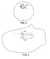
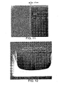
- the exposed cross section wall 404 is decorated, that is, lightly preferentially etched to show a contrast between layers of similar materials.
- the electron beam is directed toward the cross section face while an etch-enhancing gas, such as xenon difluoride, is directed toward the exposed wall of the cross section.
- the electron beam and gas preferentially etches some of the materials present on the exposed cross section face, so that the interface between materials stands out in subsequent imaging.
- xenon difluoride etches silicon oxides faster than it etches silicon nitrides and so leaves a small stair-step edge at the oxide-nitride boundary.
Landscapes
- Analytical Chemistry (AREA)
- Chemical & Material Sciences (AREA)
- Engineering & Computer Science (AREA)
- Physics & Mathematics (AREA)
- Plasma & Fusion (AREA)
- General Physics & Mathematics (AREA)
- General Engineering & Computer Science (AREA)
- Microelectronics & Electronic Packaging (AREA)
- Computer Hardware Design (AREA)
- Sampling And Sample Adjustment (AREA)
- Analysing Materials By The Use Of Radiation (AREA)
- Testing Or Measuring Of Semiconductors Or The Like (AREA)
- Investigating Materials By The Use Of Optical Means Adapted For Particular Applications (AREA)
Applications Claiming Priority (1)
| Application Number | Priority Date | Filing Date | Title |
|---|---|---|---|
| US99299807P | 2007-12-06 | 2007-12-06 |
Publications (3)
| Publication Number | Publication Date |
|---|---|
| EP2068160A2 EP2068160A2 (en) | 2009-06-10 |
| EP2068160A3 EP2068160A3 (en) | 2011-03-23 |
| EP2068160B1 true EP2068160B1 (en) | 2015-02-18 |
Family
ID=40456730
Family Applications (1)
| Application Number | Title | Priority Date | Filing Date |
|---|---|---|---|
| EP08170761.4A Not-in-force EP2068160B1 (en) | 2007-12-06 | 2008-12-05 | Apparatus and method for observing defects in semiconductor wafers |
Country Status (3)
| Country | Link |
|---|---|
| US (1) | US7858936B2 (https=) |
| EP (1) | EP2068160B1 (https=) |
| JP (2) | JP5873227B2 (https=) |
Families Citing this family (34)
| Publication number | Priority date | Publication date | Assignee | Title |
|---|---|---|---|---|
| US7138716B2 (en) * | 2003-06-27 | 2006-11-21 | Intel Corporation | Addition of metal layers with signal reallocation to a microprocessor for increased frequency and lower power |
| EP1501115B1 (en) | 2003-07-14 | 2009-07-01 | FEI Company | Dual beam system |
| US8058613B2 (en) * | 2008-10-28 | 2011-11-15 | William Marsh Rice University | Micromechanical devices for materials characterization |
| JP5649583B2 (ja) | 2008-10-31 | 2015-01-07 | エフ イー アイ カンパニFei Company | 加工終点検出方法及び装置 |
| JP5702552B2 (ja) | 2009-05-28 | 2015-04-15 | エフ イー アイ カンパニFei Company | デュアルビームシステムの制御方法 |
| NL2004888A (en) * | 2009-06-29 | 2010-12-30 | Asml Netherlands Bv | Deposition method and apparatus. |
| JP2011133176A (ja) * | 2009-12-24 | 2011-07-07 | Hitachi Kokusai Electric Inc | 標的装置 |
| DE102010003056B9 (de) | 2010-03-19 | 2014-07-31 | Carl Zeiss Microscopy Gmbh | Verfahren zur Erzeugung von Bildern einer Probe |
| US8350237B2 (en) | 2010-03-31 | 2013-01-08 | Fei Company | Automated slice milling for viewing a feature |
| DE102010024625A1 (de) * | 2010-06-22 | 2011-12-22 | Carl Zeiss Nts Gmbh | Verfahren zum Bearbeiten eines Objekts |
| JP2012242146A (ja) * | 2011-05-17 | 2012-12-10 | Hitachi High-Technologies Corp | 走査電子顕微鏡及び試料作成方法 |
| WO2013039891A1 (en) | 2011-09-12 | 2013-03-21 | Fei Company | Glancing angle mill |
| JP5969233B2 (ja) * | 2012-03-22 | 2016-08-17 | 株式会社日立ハイテクサイエンス | 断面加工観察方法及び装置 |
| US8502172B1 (en) * | 2012-06-26 | 2013-08-06 | Fei Company | Three dimensional fiducial |
| WO2014014446A1 (en) * | 2012-07-16 | 2014-01-23 | Fei Company | Endpointing for focused ion beam processing |
| KR102155834B1 (ko) * | 2012-10-05 | 2020-09-14 | 에프이아이 컴파니 | 높은 종횡비 구조 분석 |
| TWI607498B (zh) * | 2012-10-05 | 2017-12-01 | Fei公司 | 使用帶電粒子束曝露樣品中所關注特徵的方法及系統 |
| JP6355318B2 (ja) * | 2012-11-15 | 2018-07-11 | 株式会社日立ハイテクサイエンス | 断面加工観察方法及び装置 |
| US8895923B2 (en) | 2012-11-20 | 2014-11-25 | Dcg Systems, Inc. | System and method for non-contact microscopy for three-dimensional pre-characterization of a sample for fast and non-destructive on sample navigation during nanoprobing |
| EP2816585A1 (en) * | 2013-06-17 | 2014-12-24 | ICT Integrated Circuit Testing Gesellschaft für Halbleiterprüftechnik mbH | Charged particle beam system and method of operating thereof |
| JP5464535B1 (ja) * | 2013-07-23 | 2014-04-09 | 株式会社日立ハイテクノロジーズ | Ebsd検出器で所望箇所を容易に分析できる荷電粒子線装置およびその制御方法 |
| US9218940B1 (en) * | 2014-05-30 | 2015-12-22 | Fei Company | Method and apparatus for slice and view sample imaging |
| US9378927B2 (en) | 2014-09-11 | 2016-06-28 | Fei Company | AutoSlice and view undercut method |
| JP6423222B2 (ja) * | 2014-09-26 | 2018-11-14 | 株式会社日立ハイテクサイエンス | 荷電粒子ビーム装置 |
| JP6310864B2 (ja) * | 2015-01-13 | 2018-04-11 | 株式会社日立ハイテクノロジーズ | 検査装置 |
| US9978586B2 (en) * | 2015-11-06 | 2018-05-22 | Fei Company | Method of material deposition |
| DE102016002883B4 (de) * | 2016-03-09 | 2023-05-17 | Carl Zeiss Microscopy Gmbh | Verfahren zum Struktuieren eines Objekts und Partikelstrahlsystem hierzu |
| US10082470B2 (en) * | 2016-09-27 | 2018-09-25 | Kla-Tencor Corporation | Defect marking for semiconductor wafer inspection |
| JP7113613B2 (ja) * | 2016-12-21 | 2022-08-05 | エフ イー アイ カンパニ | 欠陥分析 |
| US10928740B2 (en) * | 2017-02-03 | 2021-02-23 | Kla Corporation | Three-dimensional calibration structures and methods for measuring buried defects on a three-dimensional semiconductor wafer |
| JP7719089B2 (ja) | 2020-03-13 | 2025-08-05 | カール・ツァイス・エスエムティー・ゲーエムベーハー | ウェハ中の検査ボリュームの断面画像化の方法 |
| DE102021210019A1 (de) * | 2021-09-10 | 2023-03-16 | Carl Zeiss Smt Gmbh | Verfahren und Vorrichtung zum Reparieren eines Defekts einer Probe mit einem fokussierten Teilchenstrahl |
| US11749495B2 (en) * | 2021-10-05 | 2023-09-05 | KLA Corp. | Bandpass charged particle energy filtering detector for charged particle tools |
| DE102023134499A1 (de) * | 2023-09-18 | 2025-03-20 | Raith Gmbh | Untersuchungsverfahren für eine Halbleiterprobe mittels eines Sekundärionen-Massenspektrometers mit einem fokussierten Ionenstrahl und Analysevorrichtung dafür |
Family Cites Families (23)
| Publication number | Priority date | Publication date | Assignee | Title |
|---|---|---|---|---|
| US5698397A (en) * | 1995-06-07 | 1997-12-16 | Sri International | Up-converting reporters for biological and other assays using laser excitation techniques |
| US5435850A (en) * | 1993-09-17 | 1995-07-25 | Fei Company | Gas injection system |
| JPH08329876A (ja) * | 1995-05-30 | 1996-12-13 | Hitachi Ltd | 観察試料作成方法及びその装置 |
| US5851413A (en) * | 1996-06-19 | 1998-12-22 | Micrion Corporation | Gas delivery systems for particle beam processing |
| US5990478A (en) * | 1997-07-10 | 1999-11-23 | Taiwan Semiconductor Manufacturing Co. Ltd. | Method for preparing thin specimens consisting of domains of different materials |
| JP3457875B2 (ja) * | 1998-01-27 | 2003-10-20 | 日本電子株式会社 | Fib−sem装置における試料断面観察方法およびfib−sem装置 |
| DE19859877A1 (de) * | 1998-12-23 | 2000-06-29 | Robert Magerle | Nanotomographie |
| NL1021376C1 (nl) * | 2002-09-02 | 2004-03-03 | Fei Co | Werkwijze voor het verkrijgen van een deeltjes-optische afbeelding van een sample in een deeltjes-optisch toestel. |
| US7103505B2 (en) * | 2002-11-12 | 2006-09-05 | Fei Company | Defect analyzer |
| JP2004191358A (ja) * | 2002-11-27 | 2004-07-08 | Seiko Instruments Inc | 複合荷電粒子ビームによる試料作製方法および装置 |
| JP2004226079A (ja) * | 2003-01-20 | 2004-08-12 | Seiko Instruments Inc | 表面あるいは断面加工観察方法及びその装置 |
| US6881955B2 (en) * | 2003-06-26 | 2005-04-19 | International Business Machines Corporation | Metrology process for enhancing image contrast |
| US7135123B1 (en) * | 2004-01-14 | 2006-11-14 | Credence Systems Corporation | Method and system for integrated circuit backside navigation |
| NL1027462C2 (nl) * | 2004-11-09 | 2006-05-10 | Koninkl Philips Electronics Nv | Werkwijze voor het lokaliseren van fluorescente markers. |
| JP2006221961A (ja) * | 2005-02-10 | 2006-08-24 | Seiko Epson Corp | チップの断面観察方法 |
| US7312448B2 (en) * | 2005-04-06 | 2007-12-25 | Carl Zeiss Nts Gmbh | Method and apparatus for quantitative three-dimensional reconstruction in scanning electron microscopy |
| JP4627682B2 (ja) * | 2005-05-27 | 2011-02-09 | 株式会社日立ハイテクノロジーズ | 試料作製装置および方法 |
| JP4520905B2 (ja) * | 2005-06-10 | 2010-08-11 | 株式会社日立ハイテクノロジーズ | 解析装置、プローブの制御方法および解析システム |
| US7348556B2 (en) * | 2005-07-19 | 2008-03-25 | Fei Company | Method of measuring three-dimensional surface roughness of a structure |
| EP1801593A1 (en) * | 2005-12-22 | 2007-06-27 | Koninklijke Philips Electronics N.V. | A method of imaging biological specimens using inorganic nanoparticles as label agents |
| US7709792B2 (en) * | 2006-01-12 | 2010-05-04 | Kla-Tencor Technologies Corporation | Three-dimensional imaging using electron beam activated chemical etch |
| EP1890136A1 (en) * | 2006-08-16 | 2008-02-20 | FEI Company | Method for obtaining images from slices of a specimen |
| US8835880B2 (en) * | 2006-10-31 | 2014-09-16 | Fei Company | Charged particle-beam processing using a cluster source |
-
2008
- 2008-12-03 JP JP2008308265A patent/JP5873227B2/ja active Active
- 2008-12-04 US US12/328,581 patent/US7858936B2/en active Active
- 2008-12-05 EP EP08170761.4A patent/EP2068160B1/en not_active Not-in-force
-
2014
- 2014-03-25 JP JP2014062055A patent/JP5882381B2/ja active Active
Also Published As
| Publication number | Publication date |
|---|---|
| JP5882381B2 (ja) | 2016-03-09 |
| EP2068160A3 (en) | 2011-03-23 |
| JP2014167474A (ja) | 2014-09-11 |
| EP2068160A2 (en) | 2009-06-10 |
| JP5873227B2 (ja) | 2016-03-01 |
| JP2009139379A (ja) | 2009-06-25 |
| US20090242759A1 (en) | 2009-10-01 |
| US7858936B2 (en) | 2010-12-28 |
Similar Documents
| Publication | Publication Date | Title |
|---|---|---|
| EP2068160B1 (en) | Apparatus and method for observing defects in semiconductor wafers | |
| US10529538B2 (en) | Endpointing for focused ion beam processing | |
| US10283317B2 (en) | High throughput TEM preparation processes and hardware for backside thinning of cross-sectional view lamella | |
| JP6188792B2 (ja) | Tem観察用の薄片の調製 | |
| EP1998356B1 (en) | In-Situ STEM Sample Preparation | |
| US9378925B2 (en) | TEM sample preparation | |
| WO2014106182A1 (en) | Fiducial design for tilted or glancing mill operations with a charged particle beam | |
| WO2014106200A2 (en) | Method for preparing samples for imaging | |
| US9488554B2 (en) | Method and system for reducing curtaining in charged particle beam sample preparation | |
| US9837246B1 (en) | Reinforced sample for transmission electron microscope | |
| US10410829B1 (en) | Methods for acquiring planar view stem images of device structures | |
| US10539489B2 (en) | Methods for acquiring planar view STEM images of device structures | |
| CN113945596A (zh) | 基于线的端点检测 |
Legal Events
| Date | Code | Title | Description |
|---|---|---|---|
| PUAI | Public reference made under article 153(3) epc to a published international application that has entered the european phase |
Free format text: ORIGINAL CODE: 0009012 |
|
| AK | Designated contracting states |
Kind code of ref document: A2 Designated state(s): AT BE BG CH CY CZ DE DK EE ES FI FR GB GR HR HU IE IS IT LI LT LU LV MC MT NL NO PL PT RO SE SI SK TR |
|
| AX | Request for extension of the european patent |
Extension state: AL BA MK RS |
|
| PUAL | Search report despatched |
Free format text: ORIGINAL CODE: 0009013 |
|
| AK | Designated contracting states |
Kind code of ref document: A3 Designated state(s): AT BE BG CH CY CZ DE DK EE ES FI FR GB GR HR HU IE IS IT LI LT LU LV MC MT NL NO PL PT RO SE SI SK TR |
|
| AX | Request for extension of the european patent |
Extension state: AL BA MK RS |
|
| 17P | Request for examination filed |
Effective date: 20110926 |
|
| AKX | Designation fees paid |
Designated state(s): AT BE BG CH CY CZ DE DK EE ES FI FR GB GR HR HU IE IS IT LI LT LU LV MC MT NL NO PL PT RO SE SI SK TR |
|
| RIC1 | Information provided on ipc code assigned before grant |
Ipc: G01R 31/307 20060101AFI20131114BHEP Ipc: G01N 1/00 20060101ALN20131114BHEP Ipc: H01J 37/305 20060101ALI20131114BHEP Ipc: H01J 37/304 20060101ALI20131114BHEP Ipc: H01L 21/66 20060101ALN20131114BHEP Ipc: H01J 37/26 20060101ALI20131114BHEP |
|
| GRAP | Despatch of communication of intention to grant a patent |
Free format text: ORIGINAL CODE: EPIDOSNIGR1 |
|
| RIC1 | Information provided on ipc code assigned before grant |
Ipc: G01N 1/00 20060101ALN20131210BHEP Ipc: H01L 21/66 20060101ALN20131210BHEP Ipc: H01J 37/305 20060101ALI20131210BHEP Ipc: H01J 37/304 20060101ALI20131210BHEP Ipc: H01J 37/26 20060101ALI20131210BHEP Ipc: G01R 31/307 20060101AFI20131210BHEP |
|
| INTG | Intention to grant announced |
Effective date: 20140103 |
|
| GRAP | Despatch of communication of intention to grant a patent |
Free format text: ORIGINAL CODE: EPIDOSNIGR1 |
|
| RIC1 | Information provided on ipc code assigned before grant |
Ipc: H01J 37/26 20060101ALI20140910BHEP Ipc: H01L 21/66 20060101ALN20140910BHEP Ipc: G01R 31/307 20060101AFI20140910BHEP Ipc: G01N 1/00 20060101ALN20140910BHEP Ipc: H01J 37/305 20060101ALI20140910BHEP Ipc: H01J 37/304 20060101ALI20140910BHEP |
|
| INTG | Intention to grant announced |
Effective date: 20141013 |
|
| GRAS | Grant fee paid |
Free format text: ORIGINAL CODE: EPIDOSNIGR3 |
|
| GRAA | (expected) grant |
Free format text: ORIGINAL CODE: 0009210 |
|
| AK | Designated contracting states |
Kind code of ref document: B1 Designated state(s): AT BE BG CH CY CZ DE DK EE ES FI FR GB GR HR HU IE IS IT LI LT LU LV MC MT NL NO PL PT RO SE SI SK TR |
|
| REG | Reference to a national code |
Ref country code: GB Ref legal event code: FG4D |
|
| REG | Reference to a national code |
Ref country code: CH Ref legal event code: EP |
|
| REG | Reference to a national code |
Ref country code: AT Ref legal event code: REF Ref document number: 710871 Country of ref document: AT Kind code of ref document: T Effective date: 20150315 |
|
| REG | Reference to a national code |
Ref country code: IE Ref legal event code: FG4D |
|
| REG | Reference to a national code |
Ref country code: DE Ref legal event code: R096 Ref document number: 602008036664 Country of ref document: DE Effective date: 20150402 |
|
| REG | Reference to a national code |
Ref country code: NL Ref legal event code: VDEP Effective date: 20150218 |
|
| REG | Reference to a national code |
Ref country code: AT Ref legal event code: MK05 Ref document number: 710871 Country of ref document: AT Kind code of ref document: T Effective date: 20150218 |
|
| REG | Reference to a national code |
Ref country code: LT Ref legal event code: MG4D |
|
| PG25 | Lapsed in a contracting state [announced via postgrant information from national office to epo] |
Ref country code: FI Free format text: LAPSE BECAUSE OF FAILURE TO SUBMIT A TRANSLATION OF THE DESCRIPTION OR TO PAY THE FEE WITHIN THE PRESCRIBED TIME-LIMIT Effective date: 20150218 Ref country code: SE Free format text: LAPSE BECAUSE OF FAILURE TO SUBMIT A TRANSLATION OF THE DESCRIPTION OR TO PAY THE FEE WITHIN THE PRESCRIBED TIME-LIMIT Effective date: 20150218 Ref country code: HR Free format text: LAPSE BECAUSE OF FAILURE TO SUBMIT A TRANSLATION OF THE DESCRIPTION OR TO PAY THE FEE WITHIN THE PRESCRIBED TIME-LIMIT Effective date: 20150218 Ref country code: LT Free format text: LAPSE BECAUSE OF FAILURE TO SUBMIT A TRANSLATION OF THE DESCRIPTION OR TO PAY THE FEE WITHIN THE PRESCRIBED TIME-LIMIT Effective date: 20150218 Ref country code: ES Free format text: LAPSE BECAUSE OF FAILURE TO SUBMIT A TRANSLATION OF THE DESCRIPTION OR TO PAY THE FEE WITHIN THE PRESCRIBED TIME-LIMIT Effective date: 20150218 Ref country code: NO Free format text: LAPSE BECAUSE OF FAILURE TO SUBMIT A TRANSLATION OF THE DESCRIPTION OR TO PAY THE FEE WITHIN THE PRESCRIBED TIME-LIMIT Effective date: 20150518 |
|
| PG25 | Lapsed in a contracting state [announced via postgrant information from national office to epo] |
Ref country code: IS Free format text: LAPSE BECAUSE OF FAILURE TO SUBMIT A TRANSLATION OF THE DESCRIPTION OR TO PAY THE FEE WITHIN THE PRESCRIBED TIME-LIMIT Effective date: 20150618 Ref country code: LV Free format text: LAPSE BECAUSE OF FAILURE TO SUBMIT A TRANSLATION OF THE DESCRIPTION OR TO PAY THE FEE WITHIN THE PRESCRIBED TIME-LIMIT Effective date: 20150218 Ref country code: GR Free format text: LAPSE BECAUSE OF FAILURE TO SUBMIT A TRANSLATION OF THE DESCRIPTION OR TO PAY THE FEE WITHIN THE PRESCRIBED TIME-LIMIT Effective date: 20150519 Ref country code: NL Free format text: LAPSE BECAUSE OF FAILURE TO SUBMIT A TRANSLATION OF THE DESCRIPTION OR TO PAY THE FEE WITHIN THE PRESCRIBED TIME-LIMIT Effective date: 20150218 Ref country code: AT Free format text: LAPSE BECAUSE OF FAILURE TO SUBMIT A TRANSLATION OF THE DESCRIPTION OR TO PAY THE FEE WITHIN THE PRESCRIBED TIME-LIMIT Effective date: 20150218 |
|
| PG25 | Lapsed in a contracting state [announced via postgrant information from national office to epo] |
Ref country code: SK Free format text: LAPSE BECAUSE OF FAILURE TO SUBMIT A TRANSLATION OF THE DESCRIPTION OR TO PAY THE FEE WITHIN THE PRESCRIBED TIME-LIMIT Effective date: 20150218 Ref country code: DK Free format text: LAPSE BECAUSE OF FAILURE TO SUBMIT A TRANSLATION OF THE DESCRIPTION OR TO PAY THE FEE WITHIN THE PRESCRIBED TIME-LIMIT Effective date: 20150218 Ref country code: EE Free format text: LAPSE BECAUSE OF FAILURE TO SUBMIT A TRANSLATION OF THE DESCRIPTION OR TO PAY THE FEE WITHIN THE PRESCRIBED TIME-LIMIT Effective date: 20150218 Ref country code: CZ Free format text: LAPSE BECAUSE OF FAILURE TO SUBMIT A TRANSLATION OF THE DESCRIPTION OR TO PAY THE FEE WITHIN THE PRESCRIBED TIME-LIMIT Effective date: 20150218 Ref country code: RO Free format text: LAPSE BECAUSE OF FAILURE TO SUBMIT A TRANSLATION OF THE DESCRIPTION OR TO PAY THE FEE WITHIN THE PRESCRIBED TIME-LIMIT Effective date: 20150218 |
|
| REG | Reference to a national code |
Ref country code: DE Ref legal event code: R097 Ref document number: 602008036664 Country of ref document: DE |
|
| PG25 | Lapsed in a contracting state [announced via postgrant information from national office to epo] |
Ref country code: PL Free format text: LAPSE BECAUSE OF FAILURE TO SUBMIT A TRANSLATION OF THE DESCRIPTION OR TO PAY THE FEE WITHIN THE PRESCRIBED TIME-LIMIT Effective date: 20150218 |
|
| REG | Reference to a national code |
Ref country code: FR Ref legal event code: PLFP Year of fee payment: 8 |
|
| PLBE | No opposition filed within time limit |
Free format text: ORIGINAL CODE: 0009261 |
|
| STAA | Information on the status of an ep patent application or granted ep patent |
Free format text: STATUS: NO OPPOSITION FILED WITHIN TIME LIMIT |
|
| PG25 | Lapsed in a contracting state [announced via postgrant information from national office to epo] |
Ref country code: IT Free format text: LAPSE BECAUSE OF FAILURE TO SUBMIT A TRANSLATION OF THE DESCRIPTION OR TO PAY THE FEE WITHIN THE PRESCRIBED TIME-LIMIT Effective date: 20150218 |
|
| 26N | No opposition filed |
Effective date: 20151119 |
|
| PG25 | Lapsed in a contracting state [announced via postgrant information from national office to epo] |
Ref country code: SI Free format text: LAPSE BECAUSE OF FAILURE TO SUBMIT A TRANSLATION OF THE DESCRIPTION OR TO PAY THE FEE WITHIN THE PRESCRIBED TIME-LIMIT Effective date: 20150218 |
|
| PG25 | Lapsed in a contracting state [announced via postgrant information from national office to epo] |
Ref country code: BE Free format text: LAPSE BECAUSE OF FAILURE TO SUBMIT A TRANSLATION OF THE DESCRIPTION OR TO PAY THE FEE WITHIN THE PRESCRIBED TIME-LIMIT Effective date: 20150218 |
|
| PG25 | Lapsed in a contracting state [announced via postgrant information from national office to epo] |
Ref country code: MC Free format text: LAPSE BECAUSE OF FAILURE TO SUBMIT A TRANSLATION OF THE DESCRIPTION OR TO PAY THE FEE WITHIN THE PRESCRIBED TIME-LIMIT Effective date: 20150218 Ref country code: LU Free format text: LAPSE BECAUSE OF FAILURE TO SUBMIT A TRANSLATION OF THE DESCRIPTION OR TO PAY THE FEE WITHIN THE PRESCRIBED TIME-LIMIT Effective date: 20151205 |
|
| REG | Reference to a national code |
Ref country code: CH Ref legal event code: PL |
|
| REG | Reference to a national code |
Ref country code: IE Ref legal event code: MM4A |
|
| PG25 | Lapsed in a contracting state [announced via postgrant information from national office to epo] |
Ref country code: LI Free format text: LAPSE BECAUSE OF NON-PAYMENT OF DUE FEES Effective date: 20151231 Ref country code: IE Free format text: LAPSE BECAUSE OF NON-PAYMENT OF DUE FEES Effective date: 20151205 Ref country code: CH Free format text: LAPSE BECAUSE OF NON-PAYMENT OF DUE FEES Effective date: 20151231 |
|
| REG | Reference to a national code |
Ref country code: FR Ref legal event code: PLFP Year of fee payment: 9 |
|
| PG25 | Lapsed in a contracting state [announced via postgrant information from national office to epo] |
Ref country code: HU Free format text: LAPSE BECAUSE OF FAILURE TO SUBMIT A TRANSLATION OF THE DESCRIPTION OR TO PAY THE FEE WITHIN THE PRESCRIBED TIME-LIMIT; INVALID AB INITIO Effective date: 20081205 Ref country code: BG Free format text: LAPSE BECAUSE OF FAILURE TO SUBMIT A TRANSLATION OF THE DESCRIPTION OR TO PAY THE FEE WITHIN THE PRESCRIBED TIME-LIMIT Effective date: 20150218 |
|
| PG25 | Lapsed in a contracting state [announced via postgrant information from national office to epo] |
Ref country code: CY Free format text: LAPSE BECAUSE OF FAILURE TO SUBMIT A TRANSLATION OF THE DESCRIPTION OR TO PAY THE FEE WITHIN THE PRESCRIBED TIME-LIMIT Effective date: 20150218 |
|
| PG25 | Lapsed in a contracting state [announced via postgrant information from national office to epo] |
Ref country code: MT Free format text: LAPSE BECAUSE OF FAILURE TO SUBMIT A TRANSLATION OF THE DESCRIPTION OR TO PAY THE FEE WITHIN THE PRESCRIBED TIME-LIMIT Effective date: 20150218 Ref country code: TR Free format text: LAPSE BECAUSE OF FAILURE TO SUBMIT A TRANSLATION OF THE DESCRIPTION OR TO PAY THE FEE WITHIN THE PRESCRIBED TIME-LIMIT Effective date: 20150218 |
|
| REG | Reference to a national code |
Ref country code: FR Ref legal event code: PLFP Year of fee payment: 10 |
|
| PG25 | Lapsed in a contracting state [announced via postgrant information from national office to epo] |
Ref country code: PT Free format text: LAPSE BECAUSE OF FAILURE TO SUBMIT A TRANSLATION OF THE DESCRIPTION OR TO PAY THE FEE WITHIN THE PRESCRIBED TIME-LIMIT Effective date: 20150218 |
|
| PGFP | Annual fee paid to national office [announced via postgrant information from national office to epo] |
Ref country code: DE Payment date: 20181120 Year of fee payment: 11 |
|
| PGFP | Annual fee paid to national office [announced via postgrant information from national office to epo] |
Ref country code: GB Payment date: 20181205 Year of fee payment: 11 Ref country code: FR Payment date: 20181120 Year of fee payment: 11 |
|
| REG | Reference to a national code |
Ref country code: DE Ref legal event code: R119 Ref document number: 602008036664 Country of ref document: DE |
|
| GBPC | Gb: european patent ceased through non-payment of renewal fee |
Effective date: 20191205 |
|
| PG25 | Lapsed in a contracting state [announced via postgrant information from national office to epo] |
Ref country code: DE Free format text: LAPSE BECAUSE OF NON-PAYMENT OF DUE FEES Effective date: 20200701 Ref country code: FR Free format text: LAPSE BECAUSE OF NON-PAYMENT OF DUE FEES Effective date: 20191231 Ref country code: GB Free format text: LAPSE BECAUSE OF NON-PAYMENT OF DUE FEES Effective date: 20191205 |