EP2066161A1 - Method for manufacturing substrate with built-in component and substrate with built-in component - Google Patents
Method for manufacturing substrate with built-in component and substrate with built-in component Download PDFInfo
- Publication number
- EP2066161A1 EP2066161A1 EP08752581A EP08752581A EP2066161A1 EP 2066161 A1 EP2066161 A1 EP 2066161A1 EP 08752581 A EP08752581 A EP 08752581A EP 08752581 A EP08752581 A EP 08752581A EP 2066161 A1 EP2066161 A1 EP 2066161A1
- Authority
- EP
- European Patent Office
- Prior art keywords
- layer
- component
- interlayer connection
- conductor
- connection conductor
- Prior art date
- Legal status (The legal status is an assumption and is not a legal conclusion. Google has not performed a legal analysis and makes no representation as to the accuracy of the status listed.)
- Withdrawn
Links
Images







Classifications
-
- H—ELECTRICITY
- H05—ELECTRIC TECHNIQUES NOT OTHERWISE PROVIDED FOR
- H05K—PRINTED CIRCUITS; CASINGS OR CONSTRUCTIONAL DETAILS OF ELECTRIC APPARATUS; MANUFACTURE OF ASSEMBLAGES OF ELECTRICAL COMPONENTS
- H05K1/00—Printed circuits
- H05K1/18—Printed circuits structurally associated with non-printed electric components
- H05K1/182—Printed circuits structurally associated with non-printed electric components associated with components mounted in printed circuit boards [PCB], e.g. insert-mounted components [IMC]
- H05K1/185—Printed circuits structurally associated with non-printed electric components associated with components mounted in printed circuit boards [PCB], e.g. insert-mounted components [IMC] associated with components encapsulated in the insulating substrate of the PCBs; associated with components incorporated in internal layers of multilayer circuit boards
-
- H—ELECTRICITY
- H05—ELECTRIC TECHNIQUES NOT OTHERWISE PROVIDED FOR
- H05K—PRINTED CIRCUITS; CASINGS OR CONSTRUCTIONAL DETAILS OF ELECTRIC APPARATUS; MANUFACTURE OF ASSEMBLAGES OF ELECTRICAL COMPONENTS
- H05K1/00—Printed circuits
- H05K1/18—Printed circuits structurally associated with non-printed electric components
-
- H—ELECTRICITY
- H05—ELECTRIC TECHNIQUES NOT OTHERWISE PROVIDED FOR
- H05K—PRINTED CIRCUITS; CASINGS OR CONSTRUCTIONAL DETAILS OF ELECTRIC APPARATUS; MANUFACTURE OF ASSEMBLAGES OF ELECTRICAL COMPONENTS
- H05K1/00—Printed circuits
- H05K1/18—Printed circuits structurally associated with non-printed electric components
- H05K1/182—Printed circuits structurally associated with non-printed electric components associated with components mounted in printed circuit boards [PCB], e.g. insert-mounted components [IMC]
- H05K1/185—Printed circuits structurally associated with non-printed electric components associated with components mounted in printed circuit boards [PCB], e.g. insert-mounted components [IMC] associated with components encapsulated in the insulating substrate of the PCBs; associated with components incorporated in internal layers of multilayer circuit boards
- H05K1/186—Printed circuits structurally associated with non-printed electric components associated with components mounted in printed circuit boards [PCB], e.g. insert-mounted components [IMC] associated with components encapsulated in the insulating substrate of the PCBs; associated with components incorporated in internal layers of multilayer circuit boards manufactured by mounting on or connecting to patterned circuits before or during embedding
- H05K1/187—Printed circuits structurally associated with non-printed electric components associated with components mounted in printed circuit boards [PCB], e.g. insert-mounted components [IMC] associated with components encapsulated in the insulating substrate of the PCBs; associated with components incorporated in internal layers of multilayer circuit boards manufactured by mounting on or connecting to patterned circuits before or during embedding the patterned circuits being prefabricated circuits, which are not yet attached to a permanent insulating substrate, e.g. on a temporary carrier
-
- H—ELECTRICITY
- H05—ELECTRIC TECHNIQUES NOT OTHERWISE PROVIDED FOR
- H05K—PRINTED CIRCUITS; CASINGS OR CONSTRUCTIONAL DETAILS OF ELECTRIC APPARATUS; MANUFACTURE OF ASSEMBLAGES OF ELECTRICAL COMPONENTS
- H05K3/00—Apparatus or processes for manufacturing printed circuits
- H05K3/10—Apparatus or processes for manufacturing printed circuits in which conductive material is applied to the insulating support in such a manner as to form the desired conductive pattern
- H05K3/20—Apparatus or processes for manufacturing printed circuits in which conductive material is applied to the insulating support in such a manner as to form the desired conductive pattern by affixing prefabricated conductor pattern
-
- H—ELECTRICITY
- H05—ELECTRIC TECHNIQUES NOT OTHERWISE PROVIDED FOR
- H05K—PRINTED CIRCUITS; CASINGS OR CONSTRUCTIONAL DETAILS OF ELECTRIC APPARATUS; MANUFACTURE OF ASSEMBLAGES OF ELECTRICAL COMPONENTS
- H05K3/00—Apparatus or processes for manufacturing printed circuits
- H05K3/30—Assembling printed circuits with electric components, e.g. with resistors
-
- H—ELECTRICITY
- H05—ELECTRIC TECHNIQUES NOT OTHERWISE PROVIDED FOR
- H05K—PRINTED CIRCUITS; CASINGS OR CONSTRUCTIONAL DETAILS OF ELECTRIC APPARATUS; MANUFACTURE OF ASSEMBLAGES OF ELECTRICAL COMPONENTS
- H05K3/00—Apparatus or processes for manufacturing printed circuits
- H05K3/40—Forming printed elements for providing electric connections to or between printed circuits
-
- H—ELECTRICITY
- H05—ELECTRIC TECHNIQUES NOT OTHERWISE PROVIDED FOR
- H05K—PRINTED CIRCUITS; CASINGS OR CONSTRUCTIONAL DETAILS OF ELECTRIC APPARATUS; MANUFACTURE OF ASSEMBLAGES OF ELECTRICAL COMPONENTS
- H05K2201/00—Indexing scheme relating to printed circuits covered by H05K1/00
- H05K2201/09—Shape and layout
- H05K2201/09009—Substrate related
- H05K2201/09045—Locally raised area or protrusion of insulating substrate
-
- H—ELECTRICITY
- H05—ELECTRIC TECHNIQUES NOT OTHERWISE PROVIDED FOR
- H05K—PRINTED CIRCUITS; CASINGS OR CONSTRUCTIONAL DETAILS OF ELECTRIC APPARATUS; MANUFACTURE OF ASSEMBLAGES OF ELECTRICAL COMPONENTS
- H05K2201/00—Indexing scheme relating to printed circuits covered by H05K1/00
- H05K2201/10—Details of components or other objects attached to or integrated in a printed circuit board
- H05K2201/10227—Other objects, e.g. metallic pieces
- H05K2201/10378—Interposers
-
- H—ELECTRICITY
- H05—ELECTRIC TECHNIQUES NOT OTHERWISE PROVIDED FOR
- H05K—PRINTED CIRCUITS; CASINGS OR CONSTRUCTIONAL DETAILS OF ELECTRIC APPARATUS; MANUFACTURE OF ASSEMBLAGES OF ELECTRICAL COMPONENTS
- H05K2201/00—Indexing scheme relating to printed circuits covered by H05K1/00
- H05K2201/10—Details of components or other objects attached to or integrated in a printed circuit board
- H05K2201/10613—Details of electrical connections of non-printed components, e.g. special leads
- H05K2201/10621—Components characterised by their electrical contacts
- H05K2201/10636—Leadless chip, e.g. chip capacitor or resistor
-
- H—ELECTRICITY
- H05—ELECTRIC TECHNIQUES NOT OTHERWISE PROVIDED FOR
- H05K—PRINTED CIRCUITS; CASINGS OR CONSTRUCTIONAL DETAILS OF ELECTRIC APPARATUS; MANUFACTURE OF ASSEMBLAGES OF ELECTRICAL COMPONENTS
- H05K3/00—Apparatus or processes for manufacturing printed circuits
- H05K3/40—Forming printed elements for providing electric connections to or between printed circuits
- H05K3/4038—Through-connections; Vertical interconnect access [VIA] connections
- H05K3/4053—Through-connections; Vertical interconnect access [VIA] connections by thick-film techniques
- H05K3/4069—Through-connections; Vertical interconnect access [VIA] connections by thick-film techniques for via connections in organic insulating substrates
-
- H—ELECTRICITY
- H05—ELECTRIC TECHNIQUES NOT OTHERWISE PROVIDED FOR
- H05K—PRINTED CIRCUITS; CASINGS OR CONSTRUCTIONAL DETAILS OF ELECTRIC APPARATUS; MANUFACTURE OF ASSEMBLAGES OF ELECTRICAL COMPONENTS
- H05K3/00—Apparatus or processes for manufacturing printed circuits
- H05K3/46—Manufacturing multilayer circuits
- H05K3/4611—Manufacturing multilayer circuits by laminating two or more circuit boards
- H05K3/4614—Manufacturing multilayer circuits by laminating two or more circuit boards the electrical connections between the circuit boards being made during lamination
-
- Y—GENERAL TAGGING OF NEW TECHNOLOGICAL DEVELOPMENTS; GENERAL TAGGING OF CROSS-SECTIONAL TECHNOLOGIES SPANNING OVER SEVERAL SECTIONS OF THE IPC; TECHNICAL SUBJECTS COVERED BY FORMER USPC CROSS-REFERENCE ART COLLECTIONS [XRACs] AND DIGESTS
- Y02—TECHNOLOGIES OR APPLICATIONS FOR MITIGATION OR ADAPTATION AGAINST CLIMATE CHANGE
- Y02P—CLIMATE CHANGE MITIGATION TECHNOLOGIES IN THE PRODUCTION OR PROCESSING OF GOODS
- Y02P70/00—Climate change mitigation technologies in the production process for final industrial or consumer products
- Y02P70/50—Manufacturing or production processes characterised by the final manufactured product
-
- Y—GENERAL TAGGING OF NEW TECHNOLOGICAL DEVELOPMENTS; GENERAL TAGGING OF CROSS-SECTIONAL TECHNOLOGIES SPANNING OVER SEVERAL SECTIONS OF THE IPC; TECHNICAL SUBJECTS COVERED BY FORMER USPC CROSS-REFERENCE ART COLLECTIONS [XRACs] AND DIGESTS
- Y10—TECHNICAL SUBJECTS COVERED BY FORMER USPC
- Y10T—TECHNICAL SUBJECTS COVERED BY FORMER US CLASSIFICATION
- Y10T29/00—Metal working
- Y10T29/49—Method of mechanical manufacture
- Y10T29/49002—Electrical device making
- Y10T29/49117—Conductor or circuit manufacturing
- Y10T29/49124—On flat or curved insulated base, e.g., printed circuit, etc.
- Y10T29/4913—Assembling to base an electrical component, e.g., capacitor, etc.
Definitions
- the present invention relate to a method for manufacturing a component-embedded substrate made of a resin in which a component is embedded, and to the component-embedded substrate.
- Such a component-embedded substrate includes a component-embedded layer that is prepared by mounting components on, for example, a multilayer substrate (multilayer printed circuit board), a wired transfer plate, and embedding the components in a resin.
- a hole through which in-plane conductors disposed on the upper and lower surfaces will be electrically connected is formed by a laser or the like.
- the inter wall of the hole is plated or the hole is filled with an electroconductive paste.
- an interlayer connection conductor is formed and the upper and lower in-plane conductors are electrically connected to each other.
- the hole in which the interlayer connection conductor is formed may be called a "through-hole” or a “blind hole”, depending on how the hole is formed.
- the through-hole is formed by irradiating the component-embedded layer with laser light from above with no in-plane conductor disposed on the upper or the lower surface of the component-embedded layer (see, for example, Patent Document 1).
- the through-hole is filled with an electroconductive paste and then the resin embedding the components is cured with the in-plane conductors disposed on the upper and lower surfaces.
- the component-embedded layer having the through-hole and the in-plane conductors are integrated with each other.
- the blind hole is formed by irradiating the component-embedded layer with laser light from above with the in-plane conductor disposed on the lower surface.
- components and an in-plane conductor are disposed in an uncured resin, followed by curing the resin to integrate. Then, a blind hole is formed in the component-embedded layer and filled with an electroconductive paste.
- Patent Document 1 Japanese Unexamined Patent Application Publication No. 11-220262 (paragraphs [0056]-[0064], Fig. 2 , etc.)
- the blind hole is formed with a land of the in-plane conductor used as the bottom.
- the laser light is reflected from the land and the reflected laser light cuts the resin to form the blind hole. Consequently, the diameter of the hole becomes large. Also, in order to prevent damage to the land, only weak laser light can be irradiated. This makes the shape of the hole tapered (having a trapezoidal section).
- the plating layer needs to extend to and cover the bottom of the blind hole, or when an electroconductive paste is injected from the upper surface of the component-embedded layer, the paste needs to reach the bottom of the blind hole.
- the diameter of the hole (diameter of the upper open end of the hole) must be increased. Consequently, the lands for blind holes cannot be arranged at a narrow pitch, and thus the miniaturization of the component-embedded substrate is hampered.
- An object of the present invention is to provide a method for manufacturing a component-embedded substrate that can form a highly straight interlayer connection conductor having a small diameter and thus can achieve a miniaturized substrate with high reliability, and is to provide such a component-embedded substrate.
- a method for manufacturing a component-embedded substrate of the present invention includes: the step of forming a first in-plane conductor including a plurality of lands; the step of forming a first interlayer connection conductor in a first layer made of an uncured resin at a position corresponding to a specific one of the lands; the step of embedding a component in a second layer made of an uncured resin and subsequently curing the second layer; the step of forming a second interlayer connection conductor passing through the cured second layer from the upper surface to the lower surface at a position corresponding to the first interlayer connection conductor; and the step of stacking the first in-plane conductor, the first layer, and the second layer in that order and subsequently curing the first layer, thereby integrating the first in-plane conductor, the first layer, and the second layer.
- the first in-plane conductor, the first interlayer connection conductor, and the second interlayer connection conductor are electrically connected from one to another (Claim
- a method for manufacturing a component-embedded substrate of the present invention includes the step of forming a first interlayer connection conductor in a first layer made of an uncured resin having a first in-plane conductor including a plurality of lands.
- the first interlayer connection conductor has a bottom defined by a specific one of the lands.
- the method also includes the step of embedding a component in a second layer made of an uncured resin and subsequently curing the second layer; the step of forming a second interlayer connection conductor passing through the second layer from the upper surface to the lower surface at a position corresponding to the first interlayer connection conductor; and the step of stacking the first layer and the second layer in that order and subsequently curing the first layer, thereby integrating the first layer and the second layer.
- the first in-plane conductor, the first interlayer connection conductor, and the second interlayer connection conductor are electrically connected from one to another (Claim 2).
- the method for manufacturing a component-embedded substrate according to Claim 1 or 2 may further include the step of forming a second in-plane conductor electrically connected to the second interlayer connection conductor on the upper surface of the second layer (Claim 3).
- the method for manufacturing a component-embedded substrate according to Claim 1 or 2 may further include the step of preparing an uncured third layer having a second in-plane conductor on one surface thereof and disposing the third layer on the second layer, thereby electrically connecting the second in-plane conductor to the second interlayer connection conductor (Claim 4).
- the method for manufacturing a component-embedded substrate according to any one of Claims 1 to 4 may further include the step of exposing the component after the step of embedding the component in the uncured second layer and curing the second layer (Claim 5).
- the component may be embedded in the uncured second layer after the component is mounted on an electrode formed on a transfer plate, and the transfer plate is removed from the second layer after the second layer is cured (Claim 6).
- the first layer and the second layer may be formed of the same material (Claim 7).
- a component-embedded substrate of the present invention includes: a first in-plane conductor including a plurality of lands; a first layer disposed on the first in-plane conductor; a first interlayer connection conductor formed in the first layer and electrically connected to a specific one of the lands; a second layer made of a resin embedding a component, disposed on the first layer; a second interlayer connection conductor formed in the second layer and electrically connected to the first interlayer connection conductor; and a second in-plane conductor disposed on the upper surface of the second layer and electrically connected to the second interlayer connection conductor (Claim 8).
- a component-embedded substrate of the present invention includes: a first in-plane conductor including a plurality of lands; a resin first layer disposed on the first in-plane conductor; an interlayer connection conductor formed in the first layer and electrically connected to a specific one of the lands; a second layer made of a resin embedding a component, disposed on the first layer; a second interlayer connection conductor formed in the second layer and electrically connected to the first interlayer connection conductor; a resin third layer disposed on the second layer; a third interlayer connection conductor formed in the third layer and electrically connected to the second interlayer connection conductor; and a second in-plane conductor disposed in the upper surface of the third layer and electrically connected to the third interlayer connection conductor (Claim 9).
- the second layer in the present invention embeds a component
- the second layer is higher than the other layers.
- the second layer is cured after embedding the component, and then a second interlayer connection conductor is formed in a through-hole. Consequently, the straightness of the second interlayer connection conductor can be prevented from being degraded, and the reliability of the entire component-embedded substrate can be enhanced.
- the second interlayer connection conductor is formed in the through-hole, but not a blind hole, the second interlayer connection conductor can have a small diameter. Accordingly, the component-embedded substrate can be miniaturized.
- the invention according to Claim 5 reduces the thickness of the second layer up to the height of the component, thereby forming a highly straight through-hole.
- Fig. 1 is a sectional view of a component-embedded substrate
- Figs. 2 to 5 are representations of a method for manufacturing the component-embedded substrate.
- the component-embedded substrate 40 shown in Fig. 1 includes a first in-plane conductor 2 including a plurality of lands 2a on the upper surface of a base plate 1.
- a first layer 6 made of a resin is disposed on the upper surface of the first in-plane conductor 2.
- the first layer 6 is provided with a first interlayer connection conductor 5 in it so as to be electrically connected to a specific land 2a of the plurality of lands 2a on the upper surface of the base plate 1.
- a second layer 11 made of a resin is further formed on the upper surface of the first layer 6, and in which a component 9 is embedded.
- a second interlayer connection conductor 8 is formed and electrically connected to the first interlayer connection conductor 5.
- a second in-plane conductor 13 is formed on the upper surface of the second layer 11 and electrically connected to the second interlayer connection conductor 8.
- other first interlayer connection conductors 5 are formed at the positions corresponding to the electrodes 10 of the component 9.
- These first interlayer connection conductors 5 are electrically connected to other specific lands 2a of the first in-plane conductor 2.
- the first in-plane conductor 2 and the second in-plane conductor 13 are connected through a specific first interlayer connection conductor 5 and the second interlayer connection conductor 8, and the first in-plane conductor 2 and the electrodes 10 of the component 9 are connected through other specific first interlayer connection conductors 5.
- the first in-plane conductor 2 may be formed on the surface of a base plate 1 made of a resin, a glass epoxy, a multilayer rein plate, or the like, or may be formed using a transfer plate made of, for example, SUS.
- the first layer 6 and the second layer 11 are preferably formed of a thermosetting resin, such as an epoxy resin, from the viewpoint of ease of curing. Also, a photo-curable resin that can be cured by UV light may be used. It is desirable that a material difficult to shrink with heat be selected.
- the first layer 6 and the second layer 11 are formed of the same material, so that the thermal expansion coefficient or other properties can be uniformized in the component-embedded substrate and, thus, the reliability can be enhanced.
- the first interlayer connection conductors 5 and the second interlayer connection conductor 8 are each filled with an electroconductive paste.
- the first in-plane conductor 2 and the second in-plane conductor 13 disposed in the lower surface or on the upper surface of the component-embedded substrate 40 are electrically connected to each other, and the first in-plane conductor 2 and the electrodes 10 of the component 9 embedded in the second layer 11 are electrically connected to each other.
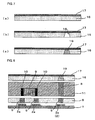
- Fig. 2 is a representation of the step of forming the first in-plane conductor 2.
- a copper foil layer 3 is formed on the upper surface of a base plate 1 shown in Fig. 2(a) , as shown in Fig. 2(b) .
- the copper foil layer 3 is patterned into a first in-plane conductor 2 including a plurality of lands 2a by, for example, etching, as shown in Fig. 2(c) .
- the first in-plane conductor 2 may be formed by plating the entire upper surface of the base plate 1 to form an electroconductive layer of an electroconductive metal, such as copper or a copper alloy, and patterning the electroconductive layer.
- the first in-plane conductor 2 can be transferred to the first layer 6 by forming and pressing an uncured first layer 6 on the transfer plate and then removing the transfer plate.
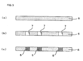
- Fig. 3 is a representation of the step of forming the first layer 6.
- An uncured resin first layer 6 shown in Fig. 3(a) is irradiated with laser light from above, corresponding to the positions of the lands 2a of the first in-plane conductor 2.
- holes 7 are formed so as to pass through the first layer 6 in the vertical direction, as shown in Fig. 3(b) .
- the holes 7 are filled with an electroconductive paste to form first interlayer connection conductors 5.
- the electroconductive paste is, for example, a resin paste containing an electroconductive material (metal).
- the inner walls of the holes 7 shown in Fig. 3(b) may be plated to form the first interlayer connection conductors 5, instead of filling the holes 7 with the electroconductive paste.
- the first interlayer connection conductors 5 may be formed by plating the inner walls of the holes 7 and subsequently filling the holes 7 with an electroconductive paste or a non-electroconductive paste, or by injecting the electroconductive paste into the holes 7 up to a predetermined height and subsequently plating the inner walls of the holes 7.
- the first layer 6 is formed thin without embedding a component or the like. Accordingly, the holes 7 are hardly deformed by the curing shrinkage of the resin even if the holes 7 are formed in the first layer 6 in an uncured state and then the first layer 6 is cured as described below.
- Fig. 4 is a representation of the step of forming the second layer 11.
- a second layer 11 made of an uncured resin is prepared, as shown in Fig. 4(a) , and a component 9, such as a chip capacitor, a chip resistor, a chip coil, or IC, is embedded in the second layer 11, as shown in Fig. 4(b) .
- reference numeral 10 designates the electrodes of the component 9.
- the second layer 11 embedding the component 9 is cured, as shown in Fig. 4(c)
- the first layer 6 is irradiated with laser light corresponding to the position of a specific first interlayer connection conductor 5 to form a hole 12 passing through the second layer 11 in the vertical direction, as shown in Fig. 4(d) .
- the hole 12 is filled with an electroconductive paste to form a second interlayer connection conductor 8.
- the inner wall of the hole 12 shown in Fig. 4(d) may be plated to form the second interlayer connection conductor 8.
- the second interlayer connection conductor 8 may be formed by filling the plated hole 12 with an electroconductive paste or a non-electroconductive paste, or by injecting the electroconductive paste into the hole 12 up to a predetermined height and subsequently plating the inner wall of the hole 12.
- the second layer 11 is preferably formed of the same thermosetting epoxy resin as the first layer 6, other thermosetting or photo-curable resins may of course be used. As with the first layer 6, a material difficult to shrink is desirably used.
- the second layer 11 Since the component 9 is embedded in the second layer 11, the second layer 11 has a certain height. Since the hole 12 is formed with the second layer 11 cured, the hole 12 is not deformed after the formation. Also, since the hole 12 is formed as a through-hole without disposing an in-plane conductor on the upper surface or the lower surface of the second layer 11, the second interlayer connection conductor 8 is not tapered, but is straight.
- the first in-plane conductor 2 including the plurality of lands 2a, the first layer 6, and the second layer 11 are integrated.
- the first in-plane conductor 2 of the base plate 1, the first layer 6, and the second layer 11 are stacked in that order and pressed to join together.
- the first layer 6 is cured to electrically connect a specific land 2a of the first in-plane conductor 2, the corresponding first interlayer connection conductor 5, and the second interlayer connection conductor 8 to one another, and other specific lands 2a, the corresponding first interlayer connection conductors 5, and the electrodes 10 of the component 9 to one another.
- the upper surface of the integrated component-embedded substrate 40 is plated with an electroconductive metal, such as copper or a copper alloy, to form an electroconductive layer.
- the electroconductive layer is patterned by etching or the like to form a second in-plane conductor 13.
- the second in-plane conductor 13 may not be patterned. If, for example, the resulting component-embedded substrate 40 is formed on the uppermost layer of a multilayer substrate, the second in-plane conductor 13 is formed over the entire upper surface of the second layer 11 so as to act as a shield electrode.
- the hole 12 is a through-hole formed without disposing an in-plane conductor on the upper surface or the lower surface.
- the diameter of the hole 12 intended for the second interlayer connection conductor 8 is therefore not increased, and accordingly narrow pitch wiring can be made.
- the straightness of the second interlayer connection conductor 8 is not degraded by the curing shrinkage of the second layer 11. Consequently, reliable wiring can be made.
- the first interlayer connection conductors 5 are formed with the first layer 6 uncured. However, the straightness of the first interlayer connection conductors 5 is hardly affected by the curing shrinkage of the first layer 6 because of the small thickness of the first layer. Therefore, the pitch can be reduced in the entire component-embedded substrate 40 and the reliability can be increased, by forming the hole 12 intended for the second interlayer connection conductor 8 with a small diameter, and by maintaining the straightness of the hole 12.
- FIG. 6 is a sectional view of a component-embedded substrate 50
- Figs. 7 and 8 are representations of a method for manufacturing the component-embedded substrate 50.
- the same reference numerals as in Figs. 1 to 5 designate the same or equivalent parts.
- the component-embedded substrate 50 of the present embodiment includes a first in-plane conductor 2, a first layer 6, and a second layer 11. While the first in-plane conductor 2, the first layer 6, and the second layer 11 have the same structure as in the first embodiment, the present embodiment is different from the first embodiment in that a third layer 16 having a second in-plane conductor 17 is provided on the second layer 11, as shown in Fig. 6 .
- Fig. 7 is a representation of the step of forming the third layer 16 on which the second in-plane conductor 17 is disposed.
- the second in-plane conductor 17 is formed of, for example, copper foil on the upper surface of the third layer 16 made of an uncured resin. Since the third layer 16 is uncured, the copper foil second in-plane conductor 17 can be easily formed by pressing the copper foil to join. Then, the third layer 16 is irradiated with laser light from below corresponding to the position of the second interlayer connection conductor 8 in the second layer 11. Thus a hole 18 is formed with the second in-plane conductor 17 used as the bottom, as shown in Fig. 7(b) . Then, the hole 18 is filled with an electroconductive paste to form a third interlayer connection conductor 19, as shown in Fig. 7(C) .
- the inner wall of the hole 18 shown in Fig. 7(b) may be plated to form the third interlayer connection conductor 19.
- the third interlayer connection conductor 19 may be formed by plating the inner wall of the hole 18 and subsequently filling the plated hole 18 with an electroconductive paste, or by injecting the electroconductive paste into the hole 18 up to a predetermined height and subsequently plating the hole 18.
- the third layer 16 is preferably formed of a thermosetting epoxy resin as the first layer 6 and the second layer 11 in the first embodiment, other thermosetting or photo-curable resins may be used. A material difficult to shrink is desirable.
- the first layer 6, the second layer 11, and the third layer 16 are formed of the same material, so that the thermal expansion coefficient and other properties can be uniformized in the component-embedded substrate and, thus, the reliability can be enhanced.
- the third layer 16 is formed thin without embedding a component. Accordingly, the hole 18 is hardly deformed by the shrinkage of the third layer 16 even if the hole 18 is formed in an uncured third layer 16 and then the third layer 16 is cured.
- the hole 18 intended for the third interlayer connection conductor 19 is a blind hole with the second in-plane conductor 17 used as the bottom, and the third interlayer connection conductor 19 is tapered as shown in Fig. 7 . Since the hole has a small thickness, however, the hole 18 is not necessarily formed to a large diameter so as to be closely filled with an electroconductive paste. Thus, the shape and diameter of the hole 18 intended for the third interlayer connection conductor 19 hardly affect the reliability and the reduction in pitch of the entire component-embedded substrate.
- the first in-plane conductor 2, the first layer 6, the second layer 11, and the third layer 16 are stacked in that order and pressed to join together.
- the first layer 6 and the third layer 16 are cured by heating or other means to electrically connect a specific land 2a of the first in-plane conductor 2, the corresponding first interlayer connection conductor 5, the second interlayer connection conductor 8, and the third interlayer connection conductor 19 to one another, and other specific lands 2a, the corresponding first interlayer connection conductors 5, and the electrodes 10 of the component 9 to one another.
- the component-embedded substrate 50 shown in Fig. 6 is assembled.
- the copper foil layer formed on the upper surface of the integrated component-embedded substrate 50 may be patterned into the second in-plane conductor 17 by, for example, etching.
- an electroconductive layer may be formed of an electroconductive metal, such as copper or a copper alloy, by plating or other means.
- a transfer plate made of, for example, SUS may be used for forming the second in-plane conductor 17.
- the second interlayer connection conductor 8 is formed with the second layer 11 cured. Consequently, the straightness of the second interlayer connection conductor 8 is not degraded. Since the hole 12 intended for the second interlayer connection conductor 8 is a through-hole, the diameter of the hole 12 is not increased. By straightly forming the second interlayer connection conductor 8 with a small diameter in the highest second layer 11, the pitch can be reduced in the entire component-embedded substrate 50 and the reliability can be enhanced.
- the third layer 16 having the second in-plane conductor 17 is provided. Consequently, the step of plating the upper surface of the second layer 11 to form an electroconductive layer is not required after integrating the first in-plane conductor 2, the first layer 6, and the second layer 11, unlike the first embodiment.
- the third interlayer connection conductor 19 is formed with the second in-plane conductor 17 used as the bottom. Thus, the reliability in continuity can be enhanced between the second in-plane conductor 17 and the third interlayer connection conductor 19.
- FIG. 9 is a sectional view of a component-embedded substrate 60
- Figs. 10 and 11 are representations of a method for manufacturing the component-embedded substrate 60.
- the same reference numerals as in Figs. 1 to 8 designate the same or equivalent parts.
- the component-embedded substrate 60 of the present embodiment is different from the component-embedded substrate 50 of the second embodiment in that the first layer 6 is stacked and pressed on the first in-plane conductor 2 to join together and subsequently first interlayer connection conductors 22 are formed with the first layer uncured, as shown in Fig. 9 .
- the second layer 11, the third 16, and the second in-plane conductor 17 are formed in the same manner as in the second embodiment.
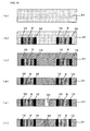
- Fig. 10 is a representation of the step of forming the first layer 6 of the present embodiment.
- a first in-plane conductor 2 including a plurality of lands 2a is formed on the upper surface of a base plate 1 in the same manner as the first in-plane conductor 2 of the first embodiment, and then an uncured resin first layer 6 is formed on the first in-plane conductor 2.
- the first in-plane conductor 2 is irradiated with laser light corresponding to the positions of the lands 2a to form holes 21 with the lands 2a used as the bottoms, as shown in Fig. 10(b) .
- first interlayer connection conductors 22 are filled with an electroconductive paste to form first interlayer connection conductors 22, as shown in Fig. 10(c) .
- the holes 21 of the first interlayer connection conductors 22 are tapered (with a trapezoidal section), there is no problem because of the small thickness of the first layer 6.
- the holes 21 may be plated instead of filling the holes 21 with an electroconductive paste.
- the first layer 6 including the first in-plane conductor 2, the second layer 11, and the third layer 16 including the second in-plane conductor 17 are integrated.
- the first layer 6 and the third layer 16 are cured by heating or other means to electrically connect a specific lands 2a of the first in-plane conductor 2, the corresponding first interlayer connection conductor 22, the second interlayer connection conductor 8, and the third interlayer connection conductor 19, and the second in-plane conductor 17 to one another, and other specific lands 2a, the corresponding first interlayer connection conductors 22, and the electrodes 10 of the component 9 are electrically connected to one another.
- the component-embedded substrate 60 shown in Fig. 9 is assembled.
- the second interlayer connection conductor 8 is formed with the second layer 11 cured. Consequently, the straightness of the second interlayer connection conductor 8 is not degraded. Since the hole 12 intended for the second interlayer connection conductor 8 is a through-hole, the diameter of the holes 12 is not increased. By straightly forming the second interlayer connection conductor 8 with a small diameter in the highest second layer 11, the pitch can be reduced in the entire component-embedded substrate 60 and the reliability can be enhanced.
- the first interlayer connection conductors 22 are formed with the first in-plane conductor 2 used as the bottoms. Consequently, the reliability in continuity can be enhanced between the first in-plane conductor 2 and the first interlayer connection conductors 22.
- first in-plane conductor 2 is formed using a transfer plate made of, for example, SUS, an uncured first layer 6 is formed and pressed on the transfer plate to join together, and the transfer plate is removed after curing the first layer 6 through predetermined steps.
- the first in-plane conductor 2 can be transferred to the first layer 6.
- FIG. 12 is a sectional view of a component-embedded substrate 70
- Figs. 13 and 14 are representations of a method for manufacturing the component-embedded substrate 70.
- the same reference numerals as in Figs. 1 to 11 designate the same or equivalent parts.
- the second in-plane conductor 17 of the component-embedded substrate 60 according to the third embodiment is replaced with a second in-plane conductor 26 formed on a transfer plate 25, as shown in Fig. 12 .
- the transfer plate 25 including the second in-plane conductor 26 is stacked and pressed on an uncured resin third layer 16 to join together.
- the second in-plane conductor 26 is embedded in the third layer 16 at this point.
- the third layer is irradiated with laser light corresponding to the positions of a plurality of lands of the second in-plane conductor 26.
- a hole (not shown) is formed with the second in-plane conductor 26 used as the bottom.
- the hole is filled with an electroconductive paste to form a third interlayer connection conductor 28.
- the first layer 6 including the first in-plane conductor 2, the second layer 11, and the third layer 16 including the second in-plane conductor 26 are stacked in that order and pressed to join together.
- the first layer 6 and the third layer 16 are cured by heading or other means to electrically connect a specific land 2a of the first in-plane conductor 2, the corresponding first interlayer connection conductor 22, the second interlayer connection conductor 8, the third interlayer connection conductor 28, and the corresponding land 26a of the second in-plane conductor 26 to one another, and other specific lands 2a, the corresponding first interlayer connection conductors 22, and the electrodes 10 of the component 9 to one another.
- the component-embedded substrate 70 shown in Fig. 12 is assembled.
- the transfer plate 25 is removed from the upper surface of the third layer 16, as shown in Fig. 14 .
- the first in-plane conductor 2 embedded in the first layer 6 may also be formed using a transfer plate, as well as the second in-plane conductor 26 embedded in the third layer 16.
- the second in-plane conductor 26 is formed using a transfer plate made of, for example, SUS, an uncured third layer 16 is formed and pressed on the transfer plate to join together, and the transfer plate 25 is removed after curing the third layer 16 by heating or other means.
- the second in-plane conductor 26 can be transferred into the third layer 16. This process does not require a step for forming the second in-plane conductor 17 by patterning after integration of the first layer 6, the second layer 11, and the third layer 16. The same can apply the first in-plane conductor 2.
- first layer 6, the second layer 11, and the third layer 16 are preferably formed of the same thermosetting epoxy resin, other thermosetting or photo-curable resins may be used. A material difficult to shrink is desirable.
- the first layer 6, the second layer 11, and the third layer 16 are formed of the same material, so that the thermal expansion coefficient and other properties can be uniformized in the component-embedded substrate and, thus, the reliability can be enhanced.
- FIG. 15 is a sectional view of a component-embedded substrate 80
- Figs. 16 to 18 are representations of a method for manufacturing the component-embedded substrate 80.
- the same reference numerals as in Figs. 1 to 14 designate the same or equivalent parts.
- the component-embedded substrate 80 of the present embodiment is substantially the same as in the first and second embodiments, but is different in that the upper surface of the second layer 31 embedding the component 9 is ground to expose the component 9 at the upper surface of the second layer 31, thus reducing the thickness of the second layer 31 before the second layer 31, the first layer 6, and the third layer 32 are integrated, as shown in Fig. 15 .
- the first layer 6 is formed in the same manner as in the first and second embodiments.
- Fig. 16 is a representation of the step of forming the second layer 31.
- an uncured resin second layer 31 is prepared, as shown in Fig. 16(a) , and components 9, such as chip capacitors, chip resistors, chip coils, and IC's, are embedded, as shown in Fig. 16(b) .
- reference numeral 10 designates the electrodes of the component 9.
- the second layer 31 embedding the component 9 is cured, as shown in Fig. 16(c) , and the upper surface of the second layer 31 is mechanically ground to expose the components 9 at the upper surface of the second layer 31, and thus the thickness of the second layer 31 is reduced.
- the second layer 31 is irradiated with laser light corresponding to the position of a specific first interlayer connection conductor 5 in the first layer 6 to form a hole 33 passing through the second layer 31 in the vertical direction. Subsequently, the hole 33 is filled with an electroconductive paste to form a second interlayer connection conductor 34, as shown in Fig. 16(f) .
- the hole 33 is formed with the second layer 31 cured, the hole 33 is not deformed after the formation. Since the hole 33 is a through-hole formed without disposing an in-plane conductor on the upper surface or the lower surfaces of the second layer 31, the second interlayer connection conductor 34 is not tapered, but is straight. In addition, the thickness of the second layer 31 is reduced to the extent that the component 9 is exposed at the upper surface of the second layer, and accordingly, the shape of the hole 33 can be straighter.
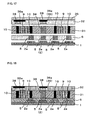
- the third layer 32 is formed in the same manner as in the modification of the third embodiment. More specifically, as shown in Fig. 17 , a transfer plate 35 including a second in-plane conductor 36 is disposed on the uncured resin third layer 32 and pressed to join together. The second in-plane conductor 36 is embedded in the third layer 32 at this point. In this state, the third layer 32 is irradiated with laser light from below corresponding to the positions of lands 36a of the second in-plane conductor 36. Thus, the holes (not shown) are formed with the second in-plane conductor 36 used as the bottoms. The holes are filled with an electroconductive paste to form third interlayer connection conductors 38.
- the first in-plane conductor 2, the first layer 6, the second layer 31, and the third layer 32 including the second in-plane conductor 36 are stacked in the order to join together.
- the first layer 6 and the third layer 32 are cured by heating or other means to electrically connect a specific land 2a of the first in-plane conductor 2, the corresponding first interlayer connection conductor 5, the second interlayer connection conductor 34, the third interlayer connection conductor 38, and the corresponding land 36a of the second in-plane conductor 36 to one another, and other specific lands 2a, the corresponding first interlayer connection conductors 5, the electrodes 10 of the components, the corresponding third interlayer connection conductor 38, and the corresponding land 36a of the second in-plane conductor 36 to one another.
- the component-embedded substrate 80 is assembled.
- the transfer plate 35 is finally removed from the upper surface of the third layer 32, as shown in Fig. 18 .
- the first in-plane conductor 2 in the first layer 6 may also be formed using a transfer plate, as well as the second in-plane conductor 36 in the third layer 32.
- the thickness of the second layer 31 is reduced before being integrated with the first layer 6 and the third layer 32. Accordingly, the second interlayer connection conductor 34 can be formed straighter, and the diameter of the hole 33 intended for the second interlayer connection conductor 34 can be reduced. Thus, the pitch can be reduced. If the electrodes 10 of the component 9 are exposed at the upper surface of the second layer 31, the electrodes 10 and the third interlayer connection conductor 38 in the third layer 32 can be electrically connected directly. Thus, wiring can be more arbitrarily performed and effective wiring becomes possible.
- the step of reducing the thickness of the second layer 31 may be performed after forming the hole 33, or after filling the hole 33 with an electroconductive paste to form the second interlayer connection conductor 34, without limiting to the time before forming the hole 33, as long as this step is performed after curing the second layer 31 embedding the component 9 and before integrating the first layer 6, the second layer 31, and the third layer 32.
- the second in-plane conductor 36 is formed using the transfer plate 35 made of, for example, SUS. This method does not require the step of patterning the second in-plane conductor 36 by etching or the like after the integration of the first layer 6, the second layer 31, and the third layer 32.
- the formation of the third layer 32 is not limited to using the transfer plate 35 as in the present embodiment.
- the second in-plane conductor may be formed by patterning a plated electroconductive layer, a copper foil, or the like, by etching or the like.
- the reduction of the thickness of the second layer 31 is not limited to mechanical grinding of the upper surface of the second layer 31, and other techniques may be applied.
- the second layer 31 may be cut to a predetermined height so that the component 9 can be exposed at the upper surface of the second layer 31.
- the electrodes 10 of the component 9 may be exposed as above, or may not be exposed.
- the inner wall of the hole 33 shown in Fig. 16(e) may be plated to form the second interlayer connection conductor 34 instead of filling the hole 33 with an electroconductive paste.
- the second interlayer connection conductor 34 may be formed by filling a plated hole 33 with an electroconductive paste or a non-electroconductive paste, or by injecting the electroconductive paste into the hole 33 up to a predetermined height and subsequently plating the inner wall of the hole 33.
- first layer 6, the second layer 31, and the third layer 32 are preferably formed of a thermosetting epoxy resin, other thermosetting or photo-curable resins may be used. A material difficult to shrink is desirably used.
- the first layer 6, the second layer 31, and the third layer 32 are formed of the same 3 material, so that the thermal expansion coefficient and other properties can be uniformized in the component-embedded substrate and, thus, the reliability can be increased.
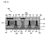
- FIG. 19 is a sectional view of a component-embedded substrate 90
- Figs. 20 to 23 are representations of a method for manufacturing the component-embedded substrate 90.
- the same reference numerals as in Figs. 1 to 18 designate the same or equivalent parts.
- the component-embedded substrate 90 of the present embodiment is substantially the same as in the fourth embodiment, but is different in that the component 9 is mounted on electrodes 42 and embedded in a resin layer in a second layer 41, as shown in Fig. 19 .
- the first layer 6, the third layer 32, and the second in-plane conductor 36 are formed in the same manner as in the fourth embodiment.
- Figs. 20 and 21 are representations of the step of forming the second layer 41.
- a transfer plate 43 including electrodes 42 as shown is Fig. 20(a) is prepared, and the component 9 is mounted with its electrodes 10 aligned with the positions corresponding to the electrodes 42, as shown in Fig. 20(b) .
- the electrodes 42 and the component 9 are embedded in an uncured second layer 41, followed by curing, as shown in Figs. 20(c) and 20(d) .
- the transfer plate 43 is removed as shown in Fig. 20(e) .
- the upper surface of the second layer 41 is ground to expose the component 9 at the upper surface of the second layer 41, as shown in Figs. 21(a) and 21(b) .
- the second layer 41 is irradiated with laser light corresponding to the position of a specific first interlayer connection conductor 5 in the first layer 6 to form a hole 44 passing through the second layer 41 in the vertical direction, as shown in Fig. 21(C) .
- the hole 44 is filled with an electroconductive paste to form a second interlayer connection conductor 45.
- the hole 44 is formed with the second layer 41 cured, the hole 44 is not deformed after the formation. Since the hole 44 is a through-hole formed without disposing an in-plane conductor on the upper or the lower surface, the second interlayer connection conductor 45 is not tapered, but is straight. In addition, the thickness of the second layer 41 is reduced to the extent that the component 9 is exposed at the upper surface of the second layer, and accordingly, the shape of the hole 44 can be straighter.
- the third layer 32 is formed in the same manner as in the fourth embodiment. More specifically, a transfer plate 35 including the second in-plane conductor 36 is disposed on the uncured resin third layer 32 and pressed to join together, as shown in Fig. 19 . The second in-plane conductor 36 is embedded in the third layer 32 at this point. In this state, the third layer 32 is irradiated with laser light from below corresponding to the positions of a plurality of lands 36a of the second in-plane conductor 36. Thus, the holes (not shown) are formed with the second in-plane conductor 36 used as the bottoms. The holes are filled with an electroconductive paste to form third interlayer connection conductors 38.
- the first in-plane conductor 2, the first layer 6, the second layer 41, and the third layer 32 are stacked in that order and pressed to join together, as shown in Fig. 22 .
- the first layer 6 and the third layer 32 are cured by heating or other means to electrically connect a specific land 2a of the first in-plane conductor 2, the corresponding first interlayer connection conductor 5, the second interlayer connection conductor 45, the corresponding third interlayer connection conductor 38, and the corresponding land 36a of the second in-plane conductor 36 to one another, and other specific lands, the corresponding first interlayer connection conductors 5, the electrodes 42, and the electrodes 10 of the components, the corresponding third interlayer connection conductor 38, and the corresponding lands 36a of the second in-plane conductor 36 to one another.
- the component-embedded substrate 90 shown in Fig. 19 is assembled and the transfer plate 35 is removed from the upper surface of the third layer 32, as shown in Fig. 23 .
- the first in-plane conductor 2 in the first layer 6 may also be formed using a transfer plate, as well as the second in-plane conductor 36 in the third layer 32.
- the component 9 is embedded in the uncured second layer 41 after being mounted on the electrode 42. Accordingly, the component 9 is difficult to displace when the second layer 41 is cured, and the first layer 6, the second layer 41, and the third layer 32 can be integrated with high positioning accuracy.
- the second interlayer connection conductor 45 can be formed straighter.
- diameter of the hole 44 intended for the second interlayer connection conductor 45 can be reduced and the pitch can be reduced.
- the electrodes 10 of the component 9 are exposed at the upper surface of the second layer 41, the electrodes 10 and the third interlayer connection conductor 38 in the third layer can be electrically connected directly.
- wiring can be more arbitrarily performed and effective wiring becomes possible.
- the step of reducing the thickness of the second layer 41 may be performed after forming the hole 44, or after filling the hole 44 with an electroconductive paste to form the second interlayer connection conductor 45, without limiting to the time before forming the hole 44, as long as this step is performed after embedding the component 9 in the second layer 41 and before integrating the first layer 6, the second layer 41, and the third layer.
- the thickness of the second layer 41 may not be reduced.
- the second in-plane conductor 36 is formed using the transfer plate 35 made of, for example, SUS. This method does not require the step of patterning the second in-plane conductor 36 by etching or the like after the integration of the first layer 6, the second layer 41, and the third layer 32.
- the formation of the third layer 32 is not limited to using the transfer plate 35 as in the present embodiment.
- the second in-plane conductor may be formed by patterning a plated electroconductive layer, a copper foil, or the like, by etching or the like.
- the reduction of the thickness of the second layer 41 is not limited to mechanical grinding of the upper surface of the second layer 41, and other techniques may be applied.
- the second layer 41 may be cut to a predetermined height so that the component 9 can be exposed at the upper surface of the second layer 41.
- the thickness of the second layer 41 may not be reduced.
- the inner wall of the hole 44 shown in Fig. 21(c) may be plated to form the second interlayer connection conductor 45, instead of filling the hole 44 with an electroconductive paste.
- the interlayer connection conductor 45 may be formed by filling a plated hole 44 with an electroconductive paste or a non-electroconductive paste, or injecting the electroconductive paste into the hole 33 up to a predetermined height and subsequently plating the inner wall of the hole 44.
- first layer 6, the second layer 41, and the third layer 32 are preferably formed of a thermosetting epoxy resin, other thermosetting or photo-curable resins may be used. A material difficult to shrink is desirably used.
- the first layer 6, the second layer 41, and the third layer 32 are formed of the same material, so that the thermal expansion coefficient and other properties can be uniformized in the component-embedded substrate and, thus, the reliability can be increased.
- the first embodiment may be modified to a form in which the first layer 6 is formed of an uncured resin on the upper surface of the base plate 1 having the first in-plane conductor 2 including a plurality of lands 2a on the upper surface, and the uncured first layer 6 is irradiated with laser light from above corresponding to the position of a specific land 2a of the first in-plane conductor 2 to form the first interlayer connection conductor 22 with the land 2a used as the bottom (corresponding to Claims 2 and 3), as in the third embodiment.
- the first interlayer connection conductor in the second, fourth, and fifth embodiments may also be formed in the same manner.
- the first layer and the second layer may be formed of the same material, and the third layer may also be formed of the same material (corresponding to Claim 7).
- the present invention can be applied to component-embedded substrates having various functions and characteristics.
Landscapes
- Engineering & Computer Science (AREA)
- Microelectronics & Electronic Packaging (AREA)
- Manufacturing & Machinery (AREA)
- Production Of Multi-Layered Print Wiring Board (AREA)
- Printing Elements For Providing Electric Connections Between Printed Circuits (AREA)
Abstract
To provide a method for manufacturing a component-embedded substrate that can form an interlayer connection conductor having a small diameter and high straightness and thus can achieve a miniaturized component-embedded substrate including interlayer connection conductors at a narrow pitch, and the component-embedded substrate. In a component-embedded substrate 40, a component 9 is embedded in an uncured resin layer 11 of a second layer 11.
After curing the resin layer 11, a hole 12 passing through the second layer 11 in the vertical direction is formed. The hole 12 is filled with an electroconductive paste to form a second interlayer connection conductor 8. A first in-plane conductor 2 including a plurality of lands 2a, a first layer 6, and the second layer 11 are stacked in that order and pressed to join together, and the first layer 6 is heated to form an integrated structure.
Description
- The present invention relate to a method for manufacturing a component-embedded substrate made of a resin in which a component is embedded, and to the component-embedded substrate.
- As electronic apparatuses are being miniaturized and sophisticated, various component-embedded substrates have been proposed which closely contains electronic components, such as capacitors, chip resistors, chip coils, and IC's, with high functionality.
- Such a component-embedded substrate includes a component-embedded layer that is prepared by mounting components on, for example, a multilayer substrate (multilayer printed circuit board), a wired transfer plate, and embedding the components in a resin. In the component-embedded layer, a hole through which in-plane conductors disposed on the upper and lower surfaces will be electrically connected is formed by a laser or the like. In order to give electroconductivity to the hole, the inter wall of the hole is plated or the hole is filled with an electroconductive paste. Thus, an interlayer connection conductor is formed and the upper and lower in-plane conductors are electrically connected to each other.
- The hole in which the interlayer connection conductor is formed may be called a "through-hole" or a "blind hole", depending on how the hole is formed.
- The through-hole is formed by irradiating the component-embedded layer with laser light from above with no in-plane conductor disposed on the upper or the lower surface of the component-embedded layer (see, for example, Patent Document 1). In
Patent Document 1, the through-hole is filled with an electroconductive paste and then the resin embedding the components is cured with the in-plane conductors disposed on the upper and lower surfaces. Thus, the component-embedded layer having the through-hole and the in-plane conductors are integrated with each other. - The blind hole is formed by irradiating the component-embedded layer with laser light from above with the in-plane conductor disposed on the lower surface. For example, components and an in-plane conductor are disposed in an uncured resin, followed by curing the resin to integrate. Then, a blind hole is formed in the component-embedded layer and filled with an electroconductive paste.
- Patent Document 1: Japanese Unexamined Patent Application Publication No.
11-220262 Fig. 2 , etc.) - When a through-hole is formed as described in
Patent Document 1, the through-hole is formed in an uncured resin, then the in-plane conductors and the component-embedded layer are integrated, and the resin is cured. Since the resin is shrunk when being cured, however, the straightness of the through-hole is reduced to cause displacement from the land of the in-plane conductor. - The blind hole is formed with a land of the in-plane conductor used as the bottom. When laser light is irradiated to form a blind hole, the laser light is reflected from the land and the reflected laser light cuts the resin to form the blind hole. Consequently, the diameter of the hole becomes large. Also, in order to prevent damage to the land, only weak laser light can be irradiated. This makes the shape of the hole tapered (having a trapezoidal section). When the hole in this state is plated from the upper surface of the component-embedded layer, the plating layer needs to extend to and cover the bottom of the blind hole, or when an electroconductive paste is injected from the upper surface of the component-embedded layer, the paste needs to reach the bottom of the blind hole. In order to cover the bottom of the blind hole as above, the diameter of the hole (diameter of the upper open end of the hole) must be increased. Consequently, the lands for blind holes cannot be arranged at a narrow pitch, and thus the miniaturization of the component-embedded substrate is hampered.
- An object of the present invention is to provide a method for manufacturing a component-embedded substrate that can form a highly straight interlayer connection conductor having a small diameter and thus can achieve a miniaturized substrate with high reliability, and is to provide such a component-embedded substrate.
- Accordingly, a method for manufacturing a component-embedded substrate of the present invention includes: the step of forming a first in-plane conductor including a plurality of lands; the step of forming a first interlayer connection conductor in a first layer made of an uncured resin at a position corresponding to a specific one of the lands; the step of embedding a component in a second layer made of an uncured resin and subsequently curing the second layer; the step of forming a second interlayer connection conductor passing through the cured second layer from the upper surface to the lower surface at a position corresponding to the first interlayer connection conductor; and the step of stacking the first in-plane conductor, the first layer, and the second layer in that order and subsequently curing the first layer, thereby integrating the first in-plane conductor, the first layer, and the second layer. Thus, the first in-plane conductor, the first interlayer connection conductor, and the second interlayer connection conductor are electrically connected from one to another (Claim 1).
- A method for manufacturing a component-embedded substrate of the present invention includes the step of forming a first interlayer connection conductor in a first layer made of an uncured resin having a first in-plane conductor including a plurality of lands. The first interlayer connection conductor has a bottom defined by a specific one of the lands. The method also includes the step of embedding a component in a second layer made of an uncured resin and subsequently curing the second layer; the step of forming a second interlayer connection conductor passing through the second layer from the upper surface to the lower surface at a position corresponding to the first interlayer connection conductor; and the step of stacking the first layer and the second layer in that order and subsequently curing the first layer, thereby integrating the first layer and the second layer. Thus, the first in-plane conductor, the first interlayer connection conductor, and the second interlayer connection conductor are electrically connected from one to another (Claim 2).
- The method for manufacturing a component-embedded substrate according to
Claim - The method for manufacturing a component-embedded substrate according to
Claim - The method for manufacturing a component-embedded substrate according to any one of
Claims 1 to 4 may further include the step of exposing the component after the step of embedding the component in the uncured second layer and curing the second layer (Claim 5). - In the method for manufacturing a component-embedded substrate according to any one of
Claims 1 to 5, the component may be embedded in the uncured second layer after the component is mounted on an electrode formed on a transfer plate, and the transfer plate is removed from the second layer after the second layer is cured (Claim 6). - In the method for manufacturing a component-embedded substrate according to any one of
Claims 1 to 6, the first layer and the second layer may be formed of the same material (Claim 7). - A component-embedded substrate of the present invention includes: a first in-plane conductor including a plurality of lands; a first layer disposed on the first in-plane conductor; a first interlayer connection conductor formed in the first layer and electrically connected to a specific one of the lands; a second layer made of a resin embedding a component, disposed on the first layer; a second interlayer connection conductor formed in the second layer and electrically connected to the first interlayer connection conductor; and a second in-plane conductor disposed on the upper surface of the second layer and electrically connected to the second interlayer connection conductor (Claim 8).
- A component-embedded substrate of the present invention includes: a first in-plane conductor including a plurality of lands; a resin first layer disposed on the first in-plane conductor; an interlayer connection conductor formed in the first layer and electrically connected to a specific one of the lands; a second layer made of a resin embedding a component, disposed on the first layer; a second interlayer connection conductor formed in the second layer and electrically connected to the first interlayer connection conductor; a resin third layer disposed on the second layer; a third interlayer connection conductor formed in the third layer and electrically connected to the second interlayer connection conductor; and a second in-plane conductor disposed in the upper surface of the third layer and electrically connected to the third interlayer connection conductor (Claim 9).
- Since the second layer in the present invention embeds a component, the second layer is higher than the other layers. In the method of the present invention, the second layer is cured after embedding the component, and then a second interlayer connection conductor is formed in a through-hole. Consequently, the straightness of the second interlayer connection conductor can be prevented from being degraded, and the reliability of the entire component-embedded substrate can be enhanced. Also, since the second interlayer connection conductor is formed in the through-hole, but not a blind hole, the second interlayer connection conductor can have a small diameter. Accordingly, the component-embedded substrate can be miniaturized. In particular, the invention according to
Claim 5 reduces the thickness of the second layer up to the height of the component, thereby forming a highly straight through-hole. -
-
Fig. 1 is a sectional view of a component-embedded substrate according to a first embodiment of the invention. -
Fig. 2 is a representation of the step of forming a first in-plane conductor of the component-embedded substrate shown inFig. 1 . -
Fig. 3 is a representation of the step of forming a first layer of the component-embedded substrate shown inFig. 1 . -
Fig. 4 is a representation of the step of forming a second layer of the component-embedded substrate shown inFig. 1 . -
Fig. 5 is a sectional view of the first in-plane conductor, the first layer, and the second layer of the component-embedded substrate shown inFig. 1 before they are integrated. -
Fig. 6 is a sectional view of a component-embedded substrate according to a second embodiment. -
Fig. 7 is a representation of the step of forming a third layer of the component-embedded substrate shown inFig. 6 . -
Fig. 8 is a sectional view of the first in-plane conductor, the first layer, the second layer, and the third layer of the component-embedded substrate shown inFig, 6 before they are integrated. -
Fig. 9 is a sectional view of a component-embedded substrate according to a third embodiment. -
Fig. 10 is a representation of the step of forming the first layer of the component-embedded substrate shown inFig. 9 . -
Fig. 11 is a sectional view of the first layer, the second layer, and the third layer of the component-embedded substrate shown inFig. 9 before they are integrated. -
Fig. 12 is a sectional view of a modification of the component-embedded substrate according to the third embodiment. -
Fig. 13 is a sectional view of the first layer, the second layer, and the third layer of the component-embedded substrate shown inFig. 12 before they are integrated. -
Fig. 14 is a sectional view of the component-embedded substrate shown inFig. 12 after removing a transfer plate. -
Fig. 15 is a sectional view of a component-embedded substrate according to a fourth embodiment. -
Fig. 16 is a representation of the step of forming the second layer of the component-embedded substrate shown inFig. 15 . -
Fig. 17 is a sectional view of the first layer, the second layer, and the third layer of the component-embedded substrate shown inFig. 15 before they are integrated. -
Fig. 18 is a sectional view of the component-embedded substrate shown inFig. 15 after removing a transfer plate. -
Fig. 19 is a sectional view of a component-embedded substrate according to a fifth embodiment. -
Fig. 20 is a representation of the step of forming the second layer of the component-embedded substrate shown inFig. 19 . -
Fig. 21 is a representation of the step of forming the second layer of the component-embedded substrate shown inFig. 19 . -
Fig. 22 is a sectional view of the first layer, the second layer, and the third layer of the component-embedded substrate shown inFig. 19 before they are integrated. -
Fig. 23 is a sectional view of the component-embedded substrate ShownFig. 19 after removing a transfer plate. -
- 2
- first in-plane conductor
- 2a
- land
- 5, 22
- first interlayer connection conductor
- 6
- first layer
- 8, 34, 35
- second interlayer connection conductor
- 9
- component
- 11, 31, 41
- second layer
- 16, 32
- third layer
- 17, 26, 36
- second in-plane conductor
- 19, 28, 39
- third interlayer connection conductor
- 26a, 36a
- land
- 42
- electrode
- 40, 50, 60, 70, 80, 90
- component-embedded substrate
- A first embodiment according to
Claims Figs. 1 to 5 .Fig. 1 is a sectional view of a component-embedded substrate, andFigs. 2 to 5 are representations of a method for manufacturing the component-embedded substrate. - The component-embedded
substrate 40 shown inFig. 1 includes a first in-plane conductor 2 including a plurality oflands 2a on the upper surface of abase plate 1. Afirst layer 6 made of a resin is disposed on the upper surface of the first in-plane conductor 2. Thefirst layer 6 is provided with a firstinterlayer connection conductor 5 in it so as to be electrically connected to aspecific land 2a of the plurality oflands 2a on the upper surface of thebase plate 1. Asecond layer 11 made of a resin is further formed on the upper surface of thefirst layer 6, and in which acomponent 9 is embedded. Also, a secondinterlayer connection conductor 8 is formed and electrically connected to the firstinterlayer connection conductor 5. A second in-plane conductor 13 is formed on the upper surface of thesecond layer 11 and electrically connected to the secondinterlayer connection conductor 8. In thefirst layer 6, other firstinterlayer connection conductors 5 are formed at the positions corresponding to theelectrodes 10 of thecomponent 9. These firstinterlayer connection conductors 5 are electrically connected to otherspecific lands 2a of the first in-plane conductor 2. In other words, the first in-plane conductor 2 and the second in-plane conductor 13 are connected through a specific firstinterlayer connection conductor 5 and the secondinterlayer connection conductor 8, and the first in-plane conductor 2 and theelectrodes 10 of thecomponent 9 are connected through other specific firstinterlayer connection conductors 5. - The first in-
plane conductor 2 may be formed on the surface of abase plate 1 made of a resin, a glass epoxy, a multilayer rein plate, or the like, or may be formed using a transfer plate made of, for example, SUS. - The
first layer 6 and thesecond layer 11 are preferably formed of a thermosetting resin, such as an epoxy resin, from the viewpoint of ease of curing. Also, a photo-curable resin that can be cured by UV light may be used. It is desirable that a material difficult to shrink with heat be selected. Preferably, thefirst layer 6 and thesecond layer 11 are formed of the same material, so that the thermal expansion coefficient or other properties can be uniformized in the component-embedded substrate and, thus, the reliability can be enhanced. - The first
interlayer connection conductors 5 and the secondinterlayer connection conductor 8 are each filled with an electroconductive paste. Thus, the first in-plane conductor 2 and the second in-plane conductor 13 disposed in the lower surface or on the upper surface of the component-embeddedsubstrate 40 are electrically connected to each other, and the first in-plane conductor 2 and theelectrodes 10 of thecomponent 9 embedded in thesecond layer 11 are electrically connected to each other. - Then, a method for manufacturing the component-embedded
substrate 40 will now be described. -
Fig. 2 is a representation of the step of forming the first in-plane conductor 2. First, a copper foil layer 3 is formed on the upper surface of abase plate 1 shown inFig. 2(a) , as shown inFig. 2(b) . Then, the copper foil layer 3 is patterned into a first in-plane conductor 2 including a plurality oflands 2a by, for example, etching, as shown inFig. 2(c) . Alternatively, the first in-plane conductor 2 may be formed by plating the entire upper surface of thebase plate 1 to form an electroconductive layer of an electroconductive metal, such as copper or a copper alloy, and patterning the electroconductive layer. - If the first in-
plane conductor 2 is formed using a transfer plate made of, for example, SUS, the first in-plane conductor 2 can be transferred to thefirst layer 6 by forming and pressing an uncuredfirst layer 6 on the transfer plate and then removing the transfer plate. -
Fig. 3 is a representation of the step of forming thefirst layer 6. An uncured resinfirst layer 6 shown inFig. 3(a) is irradiated with laser light from above, corresponding to the positions of thelands 2a of the first in-plane conductor 2. Thus, holes 7 are formed so as to pass through thefirst layer 6 in the vertical direction, as shown inFig. 3(b) . Then, as shown inFig. 3(c) , theholes 7 are filled with an electroconductive paste to form firstinterlayer connection conductors 5. - In this instance, the electroconductive paste is, for example, a resin paste containing an electroconductive material (metal).
- Alternatively, the inner walls of the
holes 7 shown inFig. 3(b) may be plated to form the firstinterlayer connection conductors 5, instead of filling theholes 7 with the electroconductive paste. The firstinterlayer connection conductors 5 may be formed by plating the inner walls of theholes 7 and subsequently filling theholes 7 with an electroconductive paste or a non-electroconductive paste, or by injecting the electroconductive paste into theholes 7 up to a predetermined height and subsequently plating the inner walls of theholes 7. - The
first layer 6 is formed thin without embedding a component or the like. Accordingly, theholes 7 are hardly deformed by the curing shrinkage of the resin even if theholes 7 are formed in thefirst layer 6 in an uncured state and then thefirst layer 6 is cured as described below. -
Fig. 4 is a representation of the step of forming thesecond layer 11. First, asecond layer 11 made of an uncured resin is prepared, as shown inFig. 4(a) , and acomponent 9, such as a chip capacitor, a chip resistor, a chip coil, or IC, is embedded in thesecond layer 11, as shown inFig. 4(b) . In the figure,reference numeral 10 designates the electrodes of thecomponent 9. Then, thesecond layer 11 embedding thecomponent 9 is cured, as shown inFig. 4(c) , and thefirst layer 6 is irradiated with laser light corresponding to the position of a specific firstinterlayer connection conductor 5 to form ahole 12 passing through thesecond layer 11 in the vertical direction, as shown inFig. 4(d) . Subsequently, as shown inFig. 4(e) , thehole 12 is filled with an electroconductive paste to form a secondinterlayer connection conductor 8. - Instead of filling the
hole 12 with the electroconductive paste, the inner wall of thehole 12 shown inFig. 4(d) may be plated to form the secondinterlayer connection conductor 8. The secondinterlayer connection conductor 8 may be formed by filling the platedhole 12 with an electroconductive paste or a non-electroconductive paste, or by injecting the electroconductive paste into thehole 12 up to a predetermined height and subsequently plating the inner wall of thehole 12. - Although the
second layer 11 is preferably formed of the same thermosetting epoxy resin as thefirst layer 6, other thermosetting or photo-curable resins may of course be used. As with thefirst layer 6, a material difficult to shrink is desirably used. - Since the
component 9 is embedded in thesecond layer 11, thesecond layer 11 has a certain height. Since thehole 12 is formed with thesecond layer 11 cured, thehole 12 is not deformed after the formation. Also, since thehole 12 is formed as a through-hole without disposing an in-plane conductor on the upper surface or the lower surface of thesecond layer 11, the secondinterlayer connection conductor 8 is not tapered, but is straight. - Turning now to
Fig. 5 , the first in-plane conductor 2 including the plurality oflands 2a, thefirst layer 6, and thesecond layer 11 are integrated. In this instance, the first in-plane conductor 2 of thebase plate 1, thefirst layer 6, and thesecond layer 11 are stacked in that order and pressed to join together. In this state, thefirst layer 6 is cured to electrically connect aspecific land 2a of the first in-plane conductor 2, the corresponding firstinterlayer connection conductor 5, and the secondinterlayer connection conductor 8 to one another, and otherspecific lands 2a, the corresponding firstinterlayer connection conductors 5, and theelectrodes 10 of thecomponent 9 to one another. - Finally, the upper surface of the integrated component-embedded
substrate 40 is plated with an electroconductive metal, such as copper or a copper alloy, to form an electroconductive layer. The electroconductive layer is patterned by etching or the like to form a second in-plane conductor 13. Thus, the component-embeddedsubstrate 40 as shown inFig. 1 is completed. The second in-plane conductor 13 may not be patterned. If, for example, the resulting component-embeddedsubstrate 40 is formed on the uppermost layer of a multilayer substrate, the second in-plane conductor 13 is formed over the entire upper surface of thesecond layer 11 so as to act as a shield electrode. - In the first embodiment, as described above, the
hole 12 is a through-hole formed without disposing an in-plane conductor on the upper surface or the lower surface. The diameter of thehole 12 intended for the secondinterlayer connection conductor 8 is therefore not increased, and accordingly narrow pitch wiring can be made. Also, since the secondinterlayer connection conductor 8 is formed after curing thesecond layer 11, the straightness of the secondinterlayer connection conductor 8 is not degraded by the curing shrinkage of thesecond layer 11. Consequently, reliable wiring can be made. As described above, the firstinterlayer connection conductors 5 are formed with thefirst layer 6 uncured. However, the straightness of the firstinterlayer connection conductors 5 is hardly affected by the curing shrinkage of thefirst layer 6 because of the small thickness of the first layer. Therefore, the pitch can be reduced in the entire component-embeddedsubstrate 40 and the reliability can be increased, by forming thehole 12 intended for the secondinterlayer connection conductor 8 with a small diameter, and by maintaining the straightness of thehole 12. - A second embodiment according to
Claims Figs. 6 to 8 .Fig. 6 is a sectional view of a component-embeddedsubstrate 50, andFigs. 7 and 8 are representations of a method for manufacturing the component-embeddedsubstrate 50. InFigs. 6 to 8 , the same reference numerals as inFigs. 1 to 5 designate the same or equivalent parts. - As with the component-embedded
substrate 40 of the first embodiment, the component-embeddedsubstrate 50 of the present embodiment includes a first in-plane conductor 2, afirst layer 6, and asecond layer 11. While the first in-plane conductor 2, thefirst layer 6, and thesecond layer 11 have the same structure as in the first embodiment, the present embodiment is different from the first embodiment in that athird layer 16 having a second in-plane conductor 17 is provided on thesecond layer 11, as shown inFig. 6 . -
Fig. 7 is a representation of the step of forming thethird layer 16 on which the second in-plane conductor 17 is disposed. As shown inFig. 7(a) , the second in-plane conductor 17 is formed of, for example, copper foil on the upper surface of thethird layer 16 made of an uncured resin. Since thethird layer 16 is uncured, the copper foil second in-plane conductor 17 can be easily formed by pressing the copper foil to join. Then, thethird layer 16 is irradiated with laser light from below corresponding to the position of the secondinterlayer connection conductor 8 in thesecond layer 11. Thus ahole 18 is formed with the second in-plane conductor 17 used as the bottom, as shown inFig. 7(b) . Then, thehole 18 is filled with an electroconductive paste to form a thirdinterlayer connection conductor 19, as shown inFig. 7(C) . - Instead of filling the
hole 18 with the electroconductive paste, the inner wall of thehole 18 shown inFig. 7(b) may be plated to form the thirdinterlayer connection conductor 19. The thirdinterlayer connection conductor 19 may be formed by plating the inner wall of thehole 18 and subsequently filling the platedhole 18 with an electroconductive paste, or by injecting the electroconductive paste into thehole 18 up to a predetermined height and subsequently plating thehole 18. - Although the
third layer 16 is preferably formed of a thermosetting epoxy resin as thefirst layer 6 and thesecond layer 11 in the first embodiment, other thermosetting or photo-curable resins may be used. A material difficult to shrink is desirable. Preferably, thefirst layer 6, thesecond layer 11, and thethird layer 16 are formed of the same material, so that the thermal expansion coefficient and other properties can be uniformized in the component-embedded substrate and, thus, the reliability can be enhanced. - The
third layer 16 is formed thin without embedding a component. Accordingly, thehole 18 is hardly deformed by the shrinkage of thethird layer 16 even if thehole 18 is formed in an uncuredthird layer 16 and then thethird layer 16 is cured. Thehole 18 intended for the thirdinterlayer connection conductor 19 is a blind hole with the second in-plane conductor 17 used as the bottom, and the thirdinterlayer connection conductor 19 is tapered as shown inFig. 7 . Since the hole has a small thickness, however, thehole 18 is not necessarily formed to a large diameter so as to be closely filled with an electroconductive paste. Thus, the shape and diameter of thehole 18 intended for the thirdinterlayer connection conductor 19 hardly affect the reliability and the reduction in pitch of the entire component-embedded substrate. - Turning now to
Fig. 8 , the first in-plane conductor 2, thefirst layer 6, thesecond layer 11, and thethird layer 16 are stacked in that order and pressed to join together. In this state, thefirst layer 6 and thethird layer 16 are cured by heating or other means to electrically connect aspecific land 2a of the first in-plane conductor 2, the corresponding firstinterlayer connection conductor 5, the secondinterlayer connection conductor 8, and the thirdinterlayer connection conductor 19 to one another, and otherspecific lands 2a, the corresponding firstinterlayer connection conductors 5, and theelectrodes 10 of thecomponent 9 to one another. Thus, the component-embeddedsubstrate 50 shown inFig. 6 is assembled. - The copper foil layer formed on the upper surface of the integrated component-embedded
substrate 50 may be patterned into the second in-plane conductor 17 by, for example, etching. Alternatively, an electroconductive layer may be formed of an electroconductive metal, such as copper or a copper alloy, by plating or other means. A transfer plate made of, for example, SUS may be used for forming the second in-plane conductor 17. - In the second embodiment as well as the first embodiment, as described above, the second
interlayer connection conductor 8 is formed with thesecond layer 11 cured. Consequently, the straightness of the secondinterlayer connection conductor 8 is not degraded. Since thehole 12 intended for the secondinterlayer connection conductor 8 is a through-hole, the diameter of thehole 12 is not increased. By straightly forming the secondinterlayer connection conductor 8 with a small diameter in the highestsecond layer 11, the pitch can be reduced in the entire component-embeddedsubstrate 50 and the reliability can be enhanced. - In the second embodiment, the
third layer 16 having the second in-plane conductor 17 is provided. Consequently, the step of plating the upper surface of thesecond layer 11 to form an electroconductive layer is not required after integrating the first in-plane conductor 2, thefirst layer 6, and thesecond layer 11, unlike the first embodiment. In addition, the thirdinterlayer connection conductor 19 is formed with the second in-plane conductor 17 used as the bottom. Thus, the reliability in continuity can be enhanced between the second in-plane conductor 17 and the thirdinterlayer connection conductor 19. - A third embodiment according to
Claims 2 and 4 will be described with reference toFigs. 9 to 11 .Fig. 9 is a sectional view of a component-embeddedsubstrate 60, andFigs. 10 and11 are representations of a method for manufacturing the component-embeddedsubstrate 60. InFigs. 9 to 11 , the same reference numerals as inFigs. 1 to 8 designate the same or equivalent parts. - The component-embedded
substrate 60 of the present embodiment is different from the component-embeddedsubstrate 50 of the second embodiment in that thefirst layer 6 is stacked and pressed on the first in-plane conductor 2 to join together and subsequently firstinterlayer connection conductors 22 are formed with the first layer uncured, as shown inFig. 9 . Thesecond layer 11, the third 16, and the second in-plane conductor 17 are formed in the same manner as in the second embodiment. -
Fig. 10 is a representation of the step of forming thefirst layer 6 of the present embodiment. As shown inFig. 10(a) , a first in-plane conductor 2 including a plurality oflands 2a is formed on the upper surface of abase plate 1 in the same manner as the first in-plane conductor 2 of the first embodiment, and then an uncured resinfirst layer 6 is formed on the first in-plane conductor 2. Then, the first in-plane conductor 2 is irradiated with laser light corresponding to the positions of thelands 2a to formholes 21 with thelands 2a used as the bottoms, as shown inFig. 10(b) . Then, theholes 21 are filled with an electroconductive paste to form firstinterlayer connection conductors 22, as shown inFig. 10(c) . Although theholes 21 of the firstinterlayer connection conductors 22 are tapered (with a trapezoidal section), there is no problem because of the small thickness of thefirst layer 6. Theholes 21 may be plated instead of filling theholes 21 with an electroconductive paste. - Turning now to
Fig. 11 , thefirst layer 6 including the first in-plane conductor 2, thesecond layer 11, and thethird layer 16 including the second in-plane conductor 17 are integrated. In this state, thefirst layer 6 and thethird layer 16 are cured by heating or other means to electrically connect aspecific lands 2a of the first in-plane conductor 2, the corresponding firstinterlayer connection conductor 22, the secondinterlayer connection conductor 8, and the thirdinterlayer connection conductor 19, and the second in-plane conductor 17 to one another, and otherspecific lands 2a, the corresponding firstinterlayer connection conductors 22, and theelectrodes 10 of thecomponent 9 are electrically connected to one another. Thus, the component-embeddedsubstrate 60 shown inFig. 9 is assembled. - In the third embodiment as well, as described above, the second
interlayer connection conductor 8 is formed with thesecond layer 11 cured. Consequently, the straightness of the secondinterlayer connection conductor 8 is not degraded. Since thehole 12 intended for the secondinterlayer connection conductor 8 is a through-hole, the diameter of theholes 12 is not increased. By straightly forming the secondinterlayer connection conductor 8 with a small diameter in the highestsecond layer 11, the pitch can be reduced in the entire component-embeddedsubstrate 60 and the reliability can be enhanced. - In the second embodiment, the first
interlayer connection conductors 22 are formed with the first in-plane conductor 2 used as the bottoms. Consequently, the reliability in continuity can be enhanced between the first in-plane conductor 2 and the firstinterlayer connection conductors 22. - If the first in-
plane conductor 2 is formed using a transfer plate made of, for example, SUS, an uncuredfirst layer 6 is formed and pressed on the transfer plate to join together, and the transfer plate is removed after curing thefirst layer 6 through predetermined steps. Thus, the first in-plane conductor 2 can be transferred to thefirst layer 6. - A modification of the third embodiment according to
Clams 2 and 4 will be described with reference toFigs. 12 to 14 .Fig. 12 is a sectional view of a component-embeddedsubstrate 70, andFigs. 13 and 14 are representations of a method for manufacturing the component-embeddedsubstrate 70. InFigs. 12 to 14 , the same reference numerals as inFigs. 1 to 11 designate the same or equivalent parts. - In the component-embedded
substrate 70 of the modification, the second in-plane conductor 17 of the component-embeddedsubstrate 60 according to the third embodiment is replaced with a second in-plane conductor 26 formed on atransfer plate 25, as shown inFig. 12 . Thetransfer plate 25 including the second in-plane conductor 26 is stacked and pressed on an uncured resinthird layer 16 to join together. The second in-plane conductor 26 is embedded in thethird layer 16 at this point. In this state, the third layer is irradiated with laser light corresponding to the positions of a plurality of lands of the second in-plane conductor 26. Thus, a hole (not shown) is formed with the second in-plane conductor 26 used as the bottom. The hole is filled with an electroconductive paste to form a thirdinterlayer connection conductor 28. - Turning now to
Fig. 13 , thefirst layer 6 including the first in-plane conductor 2, thesecond layer 11, and thethird layer 16 including the second in-plane conductor 26 are stacked in that order and pressed to join together. In this state, thefirst layer 6 and thethird layer 16 are cured by heading or other means to electrically connect aspecific land 2a of the first in-plane conductor 2, the corresponding firstinterlayer connection conductor 22, the secondinterlayer connection conductor 8, the thirdinterlayer connection conductor 28, and thecorresponding land 26a of the second in-plane conductor 26 to one another, and otherspecific lands 2a, the corresponding firstinterlayer connection conductors 22, and theelectrodes 10 of thecomponent 9 to one another. Thus, the component-embeddedsubstrate 70 shown inFig. 12 is assembled. Then, thetransfer plate 25 is removed from the upper surface of thethird layer 16, as shown inFig. 14 . - In this modification, the first in-
plane conductor 2 embedded in thefirst layer 6 may also be formed using a transfer plate, as well as the second in-plane conductor 26 embedded in thethird layer 16. - If the second in-
plane conductor 26 is formed using a transfer plate made of, for example, SUS, an uncuredthird layer 16 is formed and pressed on the transfer plate to join together, and thetransfer plate 25 is removed after curing thethird layer 16 by heating or other means. Thus, the second in-plane conductor 26 can be transferred into thethird layer 16. This process does not require a step for forming the second in-plane conductor 17 by patterning after integration of thefirst layer 6, thesecond layer 11, and thethird layer 16. The same can apply the first in-plane conductor 2. - Although the
first layer 6, thesecond layer 11, and thethird layer 16 are preferably formed of the same thermosetting epoxy resin, other thermosetting or photo-curable resins may be used. A material difficult to shrink is desirable. Preferably, thefirst layer 6, thesecond layer 11, and thethird layer 16 are formed of the same material, so that the thermal expansion coefficient and other properties can be uniformized in the component-embedded substrate and, thus, the reliability can be enhanced. - A fourth embodiment according to
Clam 5 will be described with reference toFigs. 15 to 18 .Fig. 15 is a sectional view of a component-embeddedsubstrate 80, andFigs. 16 to 18 are representations of a method for manufacturing the component-embeddedsubstrate 80. InFigs. 15 to 18 , the same reference numerals as inFigs. 1 to 14 designate the same or equivalent parts. - The component-embedded
substrate 80 of the present embodiment is substantially the same as in the first and second embodiments, but is different in that the upper surface of thesecond layer 31 embedding thecomponent 9 is ground to expose thecomponent 9 at the upper surface of thesecond layer 31, thus reducing the thickness of thesecond layer 31 before thesecond layer 31, thefirst layer 6, and thethird layer 32 are integrated, as shown inFig. 15 . Thefirst layer 6 is formed in the same manner as in the first and second embodiments. -
Fig. 16 is a representation of the step of forming thesecond layer 31. First, an uncured resinsecond layer 31 is prepared, as shown inFig. 16(a) , andcomponents 9, such as chip capacitors, chip resistors, chip coils, and IC's, are embedded, as shown inFig. 16(b) . In the figure,reference numeral 10 designates the electrodes of thecomponent 9. Then, thesecond layer 31 embedding thecomponent 9 is cured, as shown inFig. 16(c) , and the upper surface of thesecond layer 31 is mechanically ground to expose thecomponents 9 at the upper surface of thesecond layer 31, and thus the thickness of thesecond layer 31 is reduced. - Turning now to
Fig. 16(e) , thesecond layer 31 is irradiated with laser light corresponding to the position of a specific firstinterlayer connection conductor 5 in thefirst layer 6 to form ahole 33 passing through thesecond layer 31 in the vertical direction. Subsequently, thehole 33 is filled with an electroconductive paste to form a secondinterlayer connection conductor 34, as shown inFig. 16(f) . - Since the
hole 33 is formed with thesecond layer 31 cured, thehole 33 is not deformed after the formation. Since thehole 33 is a through-hole formed without disposing an in-plane conductor on the upper surface or the lower surfaces of thesecond layer 31, the secondinterlayer connection conductor 34 is not tapered, but is straight. In addition, the thickness of thesecond layer 31 is reduced to the extent that thecomponent 9 is exposed at the upper surface of the second layer, and accordingly, the shape of thehole 33 can be straighter. - The
third layer 32 is formed in the same manner as in the modification of the third embodiment. More specifically, as shown inFig. 17 , atransfer plate 35 including a second in-plane conductor 36 is disposed on the uncured resinthird layer 32 and pressed to join together. The second in-plane conductor 36 is embedded in thethird layer 32 at this point. In this state, thethird layer 32 is irradiated with laser light from below corresponding to the positions oflands 36a of the second in-plane conductor 36. Thus, the holes (not shown) are formed with the second in-plane conductor 36 used as the bottoms. The holes are filled with an electroconductive paste to form thirdinterlayer connection conductors 38. - Turning now to
Fig. 17 , the first in-plane conductor 2, thefirst layer 6, thesecond layer 31, and thethird layer 32 including the second in-plane conductor 36 are stacked in the order to join together. In this state, thefirst layer 6 and thethird layer 32 are cured by heating or other means to electrically connect aspecific land 2a of the first in-plane conductor 2, the corresponding firstinterlayer connection conductor 5, the secondinterlayer connection conductor 34, the thirdinterlayer connection conductor 38, and thecorresponding land 36a of the second in-plane conductor 36 to one another, and otherspecific lands 2a, the corresponding firstinterlayer connection conductors 5, theelectrodes 10 of the components, the corresponding thirdinterlayer connection conductor 38, and thecorresponding land 36a of the second in-plane conductor 36 to one another. Thus, the component-embeddedsubstrate 80 is assembled. Thetransfer plate 35 is finally removed from the upper surface of thethird layer 32, as shown inFig. 18 . - The first in-
plane conductor 2 in thefirst layer 6 may also be formed using a transfer plate, as well as the second in-plane conductor 36 in thethird layer 32. - In the fourth embodiment, the thickness of the
second layer 31 is reduced before being integrated with thefirst layer 6 and thethird layer 32. Accordingly, the secondinterlayer connection conductor 34 can be formed straighter, and the diameter of thehole 33 intended for the secondinterlayer connection conductor 34 can be reduced. Thus, the pitch can be reduced. If theelectrodes 10 of thecomponent 9 are exposed at the upper surface of thesecond layer 31, theelectrodes 10 and the thirdinterlayer connection conductor 38 in thethird layer 32 can be electrically connected directly. Thus, wiring can be more arbitrarily performed and effective wiring becomes possible. - The step of reducing the thickness of the
second layer 31 may be performed after forming thehole 33, or after filling thehole 33 with an electroconductive paste to form the secondinterlayer connection conductor 34, without limiting to the time before forming thehole 33, as long as this step is performed after curing thesecond layer 31 embedding thecomponent 9 and before integrating thefirst layer 6, thesecond layer 31, and thethird layer 32. - In the fourth embodiment, the second in-
plane conductor 36 is formed using thetransfer plate 35 made of, for example, SUS. This method does not require the step of patterning the second in-plane conductor 36 by etching or the like after the integration of thefirst layer 6, thesecond layer 31, and thethird layer 32. - The formation of the
third layer 32 is not limited to using thetransfer plate 35 as in the present embodiment. For example, the second in-plane conductor may be formed by patterning a plated electroconductive layer, a copper foil, or the like, by etching or the like. - The reduction of the thickness of the
second layer 31 is not limited to mechanical grinding of the upper surface of thesecond layer 31, and other techniques may be applied. For example, thesecond layer 31 may be cut to a predetermined height so that thecomponent 9 can be exposed at the upper surface of thesecond layer 31. Theelectrodes 10 of thecomponent 9 may be exposed as above, or may not be exposed. - The inner wall of the
hole 33 shown inFig. 16(e) may be plated to form the secondinterlayer connection conductor 34 instead of filling thehole 33 with an electroconductive paste. The secondinterlayer connection conductor 34 may be formed by filling a platedhole 33 with an electroconductive paste or a non-electroconductive paste, or by injecting the electroconductive paste into thehole 33 up to a predetermined height and subsequently plating the inner wall of thehole 33. - Although the
first layer 6, thesecond layer 31, and thethird layer 32 are preferably formed of a thermosetting epoxy resin, other thermosetting or photo-curable resins may be used. A material difficult to shrink is desirably used. Preferably, thefirst layer 6, thesecond layer 31, and thethird layer 32 are formed of the same 3 material, so that the thermal expansion coefficient and other properties can be uniformized in the component-embedded substrate and, thus, the reliability can be increased. - A fifth embodiment according to
Claim 6 will be described with reference toFigs. 19 to 23 .Fig. 19 is a sectional view of a component-embeddedsubstrate 90, andFigs. 20 to 23 are representations of a method for manufacturing the component-embeddedsubstrate 90. InFigs. 19 to 23 , the same reference numerals as inFigs. 1 to 18 designate the same or equivalent parts. - The component-embedded
substrate 90 of the present embodiment is substantially the same as in the fourth embodiment, but is different in that thecomponent 9 is mounted onelectrodes 42 and embedded in a resin layer in asecond layer 41, as shown inFig. 19 . Thefirst layer 6, thethird layer 32, and the second in-plane conductor 36 are formed in the same manner as in the fourth embodiment. -
Figs. 20 and21 are representations of the step of forming thesecond layer 41. First, atransfer plate 43 includingelectrodes 42 as shown isFig. 20(a) is prepared, and thecomponent 9 is mounted with itselectrodes 10 aligned with the positions corresponding to theelectrodes 42, as shown inFig. 20(b) . Then, theelectrodes 42 and thecomponent 9 are embedded in an uncuredsecond layer 41, followed by curing, as shown inFigs. 20(c) and 20(d) . Then, thetransfer plate 43 is removed as shown inFig. 20(e) . - After the removal of the
transfer plate 43, the upper surface of thesecond layer 41 is ground to expose thecomponent 9 at the upper surface of thesecond layer 41, as shown inFigs. 21(a) and 21(b) . Then, thesecond layer 41 is irradiated with laser light corresponding to the position of a specific firstinterlayer connection conductor 5 in thefirst layer 6 to form ahole 44 passing through thesecond layer 41 in the vertical direction, as shown inFig. 21(C) . In addition, as shown inFig. 21(d) , thehole 44 is filled with an electroconductive paste to form a secondinterlayer connection conductor 45. - Since the
hole 44 is formed with thesecond layer 41 cured, thehole 44 is not deformed after the formation. Since thehole 44 is a through-hole formed without disposing an in-plane conductor on the upper or the lower surface, the secondinterlayer connection conductor 45 is not tapered, but is straight. In addition, the thickness of thesecond layer 41 is reduced to the extent that thecomponent 9 is exposed at the upper surface of the second layer, and accordingly, the shape of thehole 44 can be straighter. - The
third layer 32 is formed in the same manner as in the fourth embodiment. More specifically, atransfer plate 35 including the second in-plane conductor 36 is disposed on the uncured resinthird layer 32 and pressed to join together, as shown inFig. 19 . The second in-plane conductor 36 is embedded in thethird layer 32 at this point. In this state, thethird layer 32 is irradiated with laser light from below corresponding to the positions of a plurality oflands 36a of the second in-plane conductor 36. Thus, the holes (not shown) are formed with the second in-plane conductor 36 used as the bottoms. The holes are filled with an electroconductive paste to form thirdinterlayer connection conductors 38. - Then, the first in-
plane conductor 2, thefirst layer 6, thesecond layer 41, and thethird layer 32 are stacked in that order and pressed to join together, as shown inFig. 22 . In this state, thefirst layer 6 and thethird layer 32 are cured by heating or other means to electrically connect aspecific land 2a of the first in-plane conductor 2, the corresponding firstinterlayer connection conductor 5, the secondinterlayer connection conductor 45, the corresponding thirdinterlayer connection conductor 38, and thecorresponding land 36a of the second in-plane conductor 36 to one another, and other specific lands, the corresponding firstinterlayer connection conductors 5, theelectrodes 42, and theelectrodes 10 of the components, the corresponding thirdinterlayer connection conductor 38, and thecorresponding lands 36a of the second in-plane conductor 36 to one another. Thus, the component-embeddedsubstrate 90 shown inFig. 19 is assembled and thetransfer plate 35 is removed from the upper surface of thethird layer 32, as shown inFig. 23 . - The first in-
plane conductor 2 in thefirst layer 6 may also be formed using a transfer plate, as well as the second in-plane conductor 36 in thethird layer 32. - In the fifth embodiment, as described above, the
component 9 is embedded in the uncuredsecond layer 41 after being mounted on theelectrode 42. Accordingly, thecomponent 9 is difficult to displace when thesecond layer 41 is cured, and thefirst layer 6, thesecond layer 41, and thethird layer 32 can be integrated with high positioning accuracy. - Since the thickness of the
second layer 41 is reduced before being integrated with thefirst layer 6 and thethird layer 32, the secondinterlayer connection conductor 45 can be formed straighter. Thus, diameter of thehole 44 intended for the secondinterlayer connection conductor 45 can be reduced and the pitch can be reduced. If theelectrodes 10 of thecomponent 9 are exposed at the upper surface of thesecond layer 41, theelectrodes 10 and the thirdinterlayer connection conductor 38 in the third layer can be electrically connected directly. Thus, wiring can be more arbitrarily performed and effective wiring becomes possible. - The step of reducing the thickness of the
second layer 41 may be performed after forming thehole 44, or after filling thehole 44 with an electroconductive paste to form the secondinterlayer connection conductor 45, without limiting to the time before forming thehole 44, as long as this step is performed after embedding thecomponent 9 in thesecond layer 41 and before integrating thefirst layer 6, thesecond layer 41, and the third layer. The thickness of thesecond layer 41 may not be reduced. - In the fifth embodiment, the second in-
plane conductor 36 is formed using thetransfer plate 35 made of, for example, SUS. This method does not require the step of patterning the second in-plane conductor 36 by etching or the like after the integration of thefirst layer 6, thesecond layer 41, and thethird layer 32. - The formation of the
third layer 32 is not limited to using thetransfer plate 35 as in the present embodiment. For example, the second in-plane conductor may be formed by patterning a plated electroconductive layer, a copper foil, or the like, by etching or the like. - The reduction of the thickness of the
second layer 41 is not limited to mechanical grinding of the upper surface of thesecond layer 41, and other techniques may be applied. For example, thesecond layer 41 may be cut to a predetermined height so that thecomponent 9 can be exposed at the upper surface of thesecond layer 41. The thickness of thesecond layer 41 may not be reduced. - As with the first to fourth embodiments, the inner wall of the
hole 44 shown inFig. 21(c) may be plated to form the secondinterlayer connection conductor 45, instead of filling thehole 44 with an electroconductive paste. Theinterlayer connection conductor 45 may be formed by filling a platedhole 44 with an electroconductive paste or a non-electroconductive paste, or injecting the electroconductive paste into thehole 33 up to a predetermined height and subsequently plating the inner wall of thehole 44. - Although the
first layer 6, thesecond layer 41, and thethird layer 32 are preferably formed of a thermosetting epoxy resin, other thermosetting or photo-curable resins may be used. A material difficult to shrink is desirably used. Preferably, thefirst layer 6, thesecond layer 41, and thethird layer 32 are formed of the same material, so that the thermal expansion coefficient and other properties can be uniformized in the component-embedded substrate and, thus, the reliability can be increased. - The present invention is not limited to the above-describe embodiments, and various modifications may be made without departing from the scope and spirit of the invention.
- For example, the first embodiment may be modified to a form in which the
first layer 6 is formed of an uncured resin on the upper surface of thebase plate 1 having the first in-plane conductor 2 including a plurality oflands 2a on the upper surface, and the uncuredfirst layer 6 is irradiated with laser light from above corresponding to the position of aspecific land 2a of the first in-plane conductor 2 to form the firstinterlayer connection conductor 22 with theland 2a used as the bottom (corresponding toClaims 2 and 3), as in the third embodiment. The first interlayer connection conductor in the second, fourth, and fifth embodiments may also be formed in the same manner. - The first layer and the second layer may be formed of the same material, and the third layer may also be formed of the same material (corresponding to Claim 7).
- The present invention can be applied to component-embedded substrates having various functions and characteristics.
Claims (9)
- A method for manufacturing a component-embedded substrate, comprising;
the step of forming a first in-plane conductor including a plurality of lands;
the step of forming a first interlayer connection conductor in a first layer made of an uncured resin at a position corresponding to a specific one of the lands;
the step of embedding a component in a second layer made of an uncured resin and subsequently curing the second layer;
the step of forming a second interlayer connection conductor passing through the cured second layer from the upper surface to the lower surface at a position corresponding to the first interlayer connection conductor; and
the step of stacking the first in-plane conductor, the first layer, and the second layer in that order and subsequently curing the first layer, thereby integrating the first in-plane conductor, the first layer, and the second layer;
whereby the first in-plane conductor, the first interlayer connection conductor, and the second interlayer connection conductor are electrically connected from one to another. - A method for manufacturing a component-embedded substrate, comprising:the step of forming a first interlayer connection conductor in a first layer made of an uncured resin having a first in-plane conductor including a plurality of lands, the first interlayer connection conductor having a bottom defined by a specific one of the lands;the step of embedding a component in a second layer made of an uncured resin and subsequently curing the second layer;the step of forming a second interlayer connection conductor passing through the second layer from the upper surface to the lower surface at a position corresponding to the first interlayer connection conductor; andthe step of stacking the first layer and the second layer in that order and subsequently curing the first layer, thereby integrating the first layer and the second layer;whereby the first in-plane conductor, the first interlayer connection conductor, and the second interlayer connection conductor are electrically connected from one to another.
- The method for manufacturing a component-embedded substrate according to Claim 1 or 2, further comprising the step of forming a second in-plane conductor electrically connected to the second interlayer connection conductor on the upper surface of the second layer.
- The method for manufacturing a component-embedded substrate according to Claim 1 or 2, further comprising the step of preparing an uncured third layer having a second in-plane conductor on one surface thereof and disposing the third layer on the second layer, thereby electrically connecting the second in-plane conductor to the second interlayer connection conductor.
- The method for manufacturing a component-embedded substrate according to any one of Claims 1 to 4, further comprising the step of exposing the component after the step of embedding the component in the uncured second layer and curing the second layer.
- The method for manufacturing a component-embedded substrate according to any one of Claims 1 to 5, wherein the component is embedded in the uncured second layer after the component is mounted on an electrode formed on a transfer plate, and the transfer plate is removed from the second layer after the second layer is cured.
- The method for manufacturing a component-embedded substrate according to any one of Claims 1 to 6, wherein the first layer and the second layer are formed of the same material.
- A component-embedded substrate comprising:a first in-plane conductor including a plurality of lands;a first layer disposed on the first in-plane conductor;a first interlayer connection conductor formed in the first layer and electrically connected to a specific one of the lands;a second layer made of a resin in which a component is embedded, the second layer being disposed on the first layer;a second interlayer connection conductor formed in the second layer and electrically connected to the first interlayer connection conductor; anda second in-plane conductor disposed on the upper surface of the second layer and electrically connected to the second interlayer connection conductor.
- A component-embedded substrate comprising:a first in-plane conductor including a plurality of lands;a resin first layer disposed on the first in-plane conductor;an interlayer connection conductor formed in the first layer and electrically connected to a specific one of the lands;a second layer made of a resin in which a component is embedded, the second layer being disposed on the first layer;a second interlayer connection conductor formed in the second layer and electrically connected to the first interlayer connection conductor;a resin third layer disposed on the second layer;a third interlayer connection conductor formed in the third layer and electrically connected to the second interlayer connection conductor; anda second in-plane conductor disposed in the upper surface of the third layer and electrically connected to the third interlayer connection conductor.
Applications Claiming Priority (2)
| Application Number | Priority Date | Filing Date | Title |
|---|---|---|---|
| JP2007161513 | 2007-06-19 | ||
| PCT/JP2008/058698 WO2008155957A1 (en) | 2007-06-19 | 2008-05-12 | Method for manufacturing substrate with built-in component and substrate with built-in component |
Publications (2)
| Publication Number | Publication Date |
|---|---|
| EP2066161A1 true EP2066161A1 (en) | 2009-06-03 |
| EP2066161A4 EP2066161A4 (en) | 2010-11-17 |
Family
ID=40156117
Family Applications (1)
| Application Number | Title | Priority Date | Filing Date |
|---|---|---|---|
| EP08752581A Withdrawn EP2066161A4 (en) | 2007-06-19 | 2008-05-12 | Method for manufacturing substrate with built-in component and substrate with built-in component |
Country Status (6)
| Country | Link |
|---|---|
| US (1) | US20090101400A1 (en) |
| EP (1) | EP2066161A4 (en) |
| JP (1) | JPWO2008155957A1 (en) |
| KR (1) | KR20090010963A (en) |
| CN (1) | CN101543152A (en) |
| WO (1) | WO2008155957A1 (en) |
Families Citing this family (32)
| Publication number | Priority date | Publication date | Assignee | Title |
|---|---|---|---|---|
| JP5024348B2 (en) * | 2009-03-23 | 2012-09-12 | 株式会社デンソー | Method for forming resin insulation film pattern on substrate surface and semiconductor device |
| TWI405306B (en) * | 2009-07-23 | 2013-08-11 | 日月光半導體製造股份有限公司 | Semiconductor package, method of manufacturing the same, and repeating wafer encapsulant |
| CN102044417B (en) * | 2009-10-14 | 2014-06-18 | 株式会社电装 | Semiconductor device and method of forming pattern of insulating resin film on surface of substrate |
| US20110084372A1 (en) | 2009-10-14 | 2011-04-14 | Advanced Semiconductor Engineering, Inc. | Package carrier, semiconductor package, and process for fabricating same |
| US8378466B2 (en) * | 2009-11-19 | 2013-02-19 | Advanced Semiconductor Engineering, Inc. | Wafer-level semiconductor device packages with electromagnetic interference shielding |
| TWI497679B (en) * | 2009-11-27 | 2015-08-21 | 日月光半導體製造股份有限公司 | Semiconductor package and method of manufacturing same |
| TWI408785B (en) * | 2009-12-31 | 2013-09-11 | 日月光半導體製造股份有限公司 | Semiconductor package structure |
| US8569894B2 (en) | 2010-01-13 | 2013-10-29 | Advanced Semiconductor Engineering, Inc. | Semiconductor package with single sided substrate design and manufacturing methods thereof |
| US8372689B2 (en) * | 2010-01-21 | 2013-02-12 | Advanced Semiconductor Engineering, Inc. | Wafer-level semiconductor device packages with three-dimensional fan-out and manufacturing methods thereof |
| US8320134B2 (en) * | 2010-02-05 | 2012-11-27 | Advanced Semiconductor Engineering, Inc. | Embedded component substrate and manufacturing methods thereof |
| TWI419283B (en) * | 2010-02-10 | 2013-12-11 | 日月光半導體製造股份有限公司 | Package structure |
| TWI411075B (en) * | 2010-03-22 | 2013-10-01 | 日月光半導體製造股份有限公司 | Semiconductor package and method of manufacturing same |
| CN102201382B (en) * | 2010-03-26 | 2013-01-23 | 日月光半导体制造股份有限公司 | Semiconductor package and manufacturing method thereof |
| US8278746B2 (en) | 2010-04-02 | 2012-10-02 | Advanced Semiconductor Engineering, Inc. | Semiconductor device packages including connecting elements |
| US8624374B2 (en) * | 2010-04-02 | 2014-01-07 | Advanced Semiconductor Engineering, Inc. | Semiconductor device packages with fan-out and with connecting elements for stacking and manufacturing methods thereof |
| JP5581830B2 (en) * | 2010-06-11 | 2014-09-03 | 富士通株式会社 | Manufacturing method of component-embedded substrate and component-embedded substrate |
| DK2592915T3 (en) * | 2010-07-06 | 2022-04-19 | Fujikura Ltd | Manufacturing process for laminated printed circuit board |
| WO2012015084A1 (en) * | 2010-07-30 | 2012-02-02 | Lg Innotek Co., Ltd. | Printed circuit board and method of manufacturing the same |
| TWI451546B (en) | 2010-10-29 | 2014-09-01 | 日月光半導體製造股份有限公司 | Stacked package structure, package structure thereof and manufacturing method of package structure |
| US8941222B2 (en) | 2010-11-11 | 2015-01-27 | Advanced Semiconductor Engineering Inc. | Wafer level semiconductor package and manufacturing methods thereof |
| US9406658B2 (en) * | 2010-12-17 | 2016-08-02 | Advanced Semiconductor Engineering, Inc. | Embedded component device and manufacturing methods thereof |
| US9171792B2 (en) | 2011-02-28 | 2015-10-27 | Advanced Semiconductor Engineering, Inc. | Semiconductor device packages having a side-by-side device arrangement and stacking functionality |
| US8487426B2 (en) | 2011-03-15 | 2013-07-16 | Advanced Semiconductor Engineering, Inc. | Semiconductor package with embedded die and manufacturing methods thereof |
| KR101283747B1 (en) * | 2011-05-30 | 2013-07-08 | 엘지이노텍 주식회사 | The printed circuit board and the method for manufacturing the same |
| US9064883B2 (en) * | 2011-08-25 | 2015-06-23 | Intel Mobile Communications GmbH | Chip with encapsulated sides and exposed surface |
| FI20125725L (en) * | 2012-06-26 | 2013-12-27 | Tellabs Oy | Circuit board arrangement with mechanical protection |
| US8878360B2 (en) * | 2012-07-13 | 2014-11-04 | Intel Mobile Communications GmbH | Stacked fan-out semiconductor chip |
| JP5285819B1 (en) * | 2012-11-07 | 2013-09-11 | 太陽誘電株式会社 | Electronic circuit module |
| US9406552B2 (en) | 2012-12-20 | 2016-08-02 | Advanced Semiconductor Engineering, Inc. | Semiconductor device having conductive via and manufacturing process |
| CN103874346B (en) * | 2014-03-26 | 2017-02-01 | 中国科学院微电子研究所 | A method of manufacturing a circuit board |
| JP6354285B2 (en) | 2014-04-22 | 2018-07-11 | オムロン株式会社 | Resin structure in which electronic component is embedded and method for manufacturing the same |
| JP2017130581A (en) * | 2016-01-21 | 2017-07-27 | イビデン株式会社 | Printed Wiring Board |
Family Cites Families (20)
| Publication number | Priority date | Publication date | Assignee | Title |
|---|---|---|---|---|
| US4635356A (en) * | 1984-12-28 | 1987-01-13 | Kabushiki Kaisha Toshiba | Method of manufacturing a circuit module |
| JP2817487B2 (en) * | 1991-12-09 | 1998-10-30 | 株式会社村田製作所 | Chip type directional coupler |
| ATE170307T1 (en) * | 1994-05-27 | 1998-09-15 | Ake Gustafson | METHOD FOR PRODUCING AN ELECTRONIC MODULE AND MODULE PRODUCED BY THIS METHOD |
| US6038133A (en) * | 1997-11-25 | 2000-03-14 | Matsushita Electric Industrial Co., Ltd. | Circuit component built-in module and method for producing the same |
| JP2001144432A (en) * | 1999-11-02 | 2001-05-25 | Internatl Business Mach Corp <Ibm> | Method for manufacturing conductor layer on insulation layer and method for manufacturing build-up circuit board |
| JP4744689B2 (en) * | 2000-12-11 | 2011-08-10 | パナソニック株式会社 | Viscous fluid transfer device and electronic component mounting device |
| TW511405B (en) * | 2000-12-27 | 2002-11-21 | Matsushita Electric Industrial Co Ltd | Device built-in module and manufacturing method thereof |
| KR100488412B1 (en) * | 2001-06-13 | 2005-05-11 | 가부시키가이샤 덴소 | Printed wiring board with embedded electric device and method for manufacturing printed wiring board with embedded electric device |
| JP2003124380A (en) * | 2001-10-15 | 2003-04-25 | Matsushita Electric Ind Co Ltd | Electronic component built-in module and method of manufacturing the same |
| JP4392157B2 (en) * | 2001-10-26 | 2009-12-24 | パナソニック電工株式会社 | WIRING BOARD SHEET MATERIAL AND ITS MANUFACTURING METHOD, AND MULTILAYER BOARD AND ITS MANUFACTURING METHOD |
| JP3739699B2 (en) * | 2001-12-20 | 2006-01-25 | 松下電器産業株式会社 | Method and apparatus for manufacturing electronic component mounted component |
| US7176055B2 (en) * | 2001-11-02 | 2007-02-13 | Matsushita Electric Industrial Co., Ltd. | Method and apparatus for manufacturing electronic component-mounted component, and electronic component-mounted component |
| JP2003142797A (en) * | 2001-11-02 | 2003-05-16 | Matsushita Electric Ind Co Ltd | Manufacturing method of completed electronic component mounted product and completed electronic component mounted product |
| JP2003249763A (en) * | 2002-02-25 | 2003-09-05 | Fujitsu Ltd | Multilayer wiring board and manufacturing method thereof |
| US6946205B2 (en) * | 2002-04-25 | 2005-09-20 | Matsushita Electric Industrial Co., Ltd. | Wiring transfer sheet and method for producing the same, and wiring board and method for producing the same |
| JP4016340B2 (en) * | 2003-06-13 | 2007-12-05 | ソニー株式会社 | Semiconductor device, mounting structure thereof, and manufacturing method thereof |
| JP2005109307A (en) * | 2003-10-01 | 2005-04-21 | Matsushita Electric Ind Co Ltd | Circuit component built-in substrate and manufacturing method thereof |
| US7258549B2 (en) * | 2004-02-20 | 2007-08-21 | Matsushita Electric Industrial Co., Ltd. | Connection member and mount assembly and production method of the same |
| JP2005276981A (en) * | 2004-03-24 | 2005-10-06 | Matsushita Electric Ind Co Ltd | Manufacturing method of circuit component built-in module |
| WO2006011320A1 (en) * | 2004-07-30 | 2006-02-02 | Murata Manufacturing Co., Ltd. | Composite electronic component and its manufacturing method |
-
2008
- 2008-05-12 KR KR1020087025923A patent/KR20090010963A/en not_active Abandoned
- 2008-05-12 EP EP08752581A patent/EP2066161A4/en not_active Withdrawn
- 2008-05-12 JP JP2008549296A patent/JPWO2008155957A1/en active Pending
- 2008-05-12 WO PCT/JP2008/058698 patent/WO2008155957A1/en not_active Ceased
- 2008-05-12 CN CNA200880000433XA patent/CN101543152A/en active Pending
-
2009
- 2009-01-05 US US12/348,358 patent/US20090101400A1/en active Granted
Also Published As
| Publication number | Publication date |
|---|---|
| KR20090010963A (en) | 2009-01-30 |
| US20090101400A1 (en) | 2009-04-23 |
| WO2008155957A1 (en) | 2008-12-24 |
| EP2066161A4 (en) | 2010-11-17 |
| CN101543152A (en) | 2009-09-23 |
| JPWO2008155957A1 (en) | 2010-08-26 |
Similar Documents
| Publication | Publication Date | Title |
|---|---|---|
| EP2066161A1 (en) | Method for manufacturing substrate with built-in component and substrate with built-in component | |
| JP3910045B2 (en) | Method for manufacturing electronic component internal wiring board | |
| US9345142B2 (en) | Chip embedded board and method of manufacturing the same | |
| US6879493B2 (en) | Module component and method of manufacturing the same | |
| KR101976602B1 (en) | Printed circuit board and manufacturing method thereof | |
| CN100559920C (en) | Rigid and flexible circuit board | |
| KR101319902B1 (en) | Multiple resin-layered substrate and method of manufacture of multiple resin-layered substrate | |
| TWI337515B (en) | Multilayer circuit board with embedded components and method of manufacture | |
| KR20130014122A (en) | Electronic components embedded pcb and method for manufacturing thereof | |
| CN108811323B (en) | Printed circuit board and method for manufacturing the same | |
| US20150156883A1 (en) | Printed circuit board and manufacturing method thereof | |
| CN102119588A (en) | Method for manufacturing module with built-in component, and module with built-in component | |
| US20160081191A1 (en) | Printed circuit board and manufacturing method thereof | |
| KR100820633B1 (en) | Electronic circuit board and manufacturing method | |
| KR20150050454A (en) | Wiring substrate and method of manufacturing the same | |
| KR20180128766A (en) | Electronic component embedded printed circuit board | |
| KR101693747B1 (en) | Electronic components embedded substrate and manufacturing method thereof | |
| JP4720462B2 (en) | Flexible circuit board and manufacturing method thereof | |
| EP3340753B1 (en) | Method of integrating a connector member with component carrier | |
| US20140090881A1 (en) | Passive device embedded in substrate and substrate with passive device embedded therein | |
| KR102052761B1 (en) | Chip Embedded Board And Method Of Manufacturing The Same | |
| CN116326220A (en) | Method for producing a printed circuit board and printed circuit board with at least one embedded electronic component | |
| US20010039727A1 (en) | Manufacturing method for multilayer printed circuit board | |
| CN115553075A (en) | Method for producing a circuit board and circuit board with at least one embedded electronic component | |
| CN117279205A (en) | Circuit board with embedded part and manufacturing method thereof |
Legal Events
| Date | Code | Title | Description |
|---|---|---|---|
| PUAI | Public reference made under article 153(3) epc to a published international application that has entered the european phase |
Free format text: ORIGINAL CODE: 0009012 |
|
| 17P | Request for examination filed |
Effective date: 20081029 |
|
| AK | Designated contracting states |
Kind code of ref document: A1 Designated state(s): AT BE BG CH CY CZ DE DK EE ES FI FR GB GR HR HU IE IS IT LI LT LU LV MC MT NL NO PL PT RO SE SI SK TR |
|
| AX | Request for extension of the european patent |
Extension state: AL BA MK RS |
|
| A4 | Supplementary search report drawn up and despatched |
Effective date: 20101015 |
|
| STAA | Information on the status of an ep patent application or granted ep patent |
Free format text: STATUS: THE APPLICATION HAS BEEN WITHDRAWN |
|
| 18W | Application withdrawn |
Effective date: 20110809 |