EP2062296B1 - Led-halbleiterkörper und verwendung eines led-halbleiterkörpers - Google Patents
Led-halbleiterkörper und verwendung eines led-halbleiterkörpers Download PDFInfo
- Publication number
- EP2062296B1 EP2062296B1 EP07817544.5A EP07817544A EP2062296B1 EP 2062296 B1 EP2062296 B1 EP 2062296B1 EP 07817544 A EP07817544 A EP 07817544A EP 2062296 B1 EP2062296 B1 EP 2062296B1
- Authority
- EP
- European Patent Office
- Prior art keywords
- semiconductor body
- led semiconductor
- voltage
- led
- active layers
- Prior art date
- Legal status (The legal status is an assumption and is not a legal conclusion. Google has not performed a legal analysis and makes no representation as to the accuracy of the status listed.)
- Not-in-force
Links
Images

Classifications
-
- H—ELECTRICITY
- H10—SEMICONDUCTOR DEVICES; ELECTRIC SOLID-STATE DEVICES NOT OTHERWISE PROVIDED FOR
- H10H—INORGANIC LIGHT-EMITTING SEMICONDUCTOR DEVICES HAVING POTENTIAL BARRIERS
- H10H29/00—Integrated devices, or assemblies of multiple devices, comprising at least one light-emitting semiconductor element covered by group H10H20/00
- H10H29/10—Integrated devices comprising at least one light-emitting semiconductor component covered by group H10H20/00
-
- H—ELECTRICITY
- H01—ELECTRIC ELEMENTS
- H01L—SEMICONDUCTOR DEVICES NOT COVERED BY CLASS H10
- H01L24/00—Arrangements for connecting or disconnecting semiconductor or solid-state bodies; Methods or apparatus related thereto
- H01L24/01—Means for bonding being attached to, or being formed on, the surface to be connected, e.g. chip-to-package, die-attach, "first-level" interconnects; Manufacturing methods related thereto
- H01L24/18—High density interconnect [HDI] connectors; Manufacturing methods related thereto
- H01L24/23—Structure, shape, material or disposition of the high density interconnect connectors after the connecting process
- H01L24/24—Structure, shape, material or disposition of the high density interconnect connectors after the connecting process of an individual high density interconnect connector
-
- H—ELECTRICITY
- H01—ELECTRIC ELEMENTS
- H01L—SEMICONDUCTOR DEVICES NOT COVERED BY CLASS H10
- H01L25/00—Assemblies consisting of a plurality of semiconductor or other solid state devices
- H01L25/16—Assemblies consisting of a plurality of semiconductor or other solid state devices the devices being of types provided for in two or more different subclasses of H10B, H10D, H10F, H10H, H10K or H10N, e.g. forming hybrid circuits
- H01L25/167—Assemblies consisting of a plurality of semiconductor or other solid state devices the devices being of types provided for in two or more different subclasses of H10B, H10D, H10F, H10H, H10K or H10N, e.g. forming hybrid circuits comprising optoelectronic devices, e.g. LED, photodiodes
-
- H—ELECTRICITY
- H01—ELECTRIC ELEMENTS
- H01L—SEMICONDUCTOR DEVICES NOT COVERED BY CLASS H10
- H01L2224/00—Indexing scheme for arrangements for connecting or disconnecting semiconductor or solid-state bodies and methods related thereto as covered by H01L24/00
- H01L2224/01—Means for bonding being attached to, or being formed on, the surface to be connected, e.g. chip-to-package, die-attach, "first-level" interconnects; Manufacturing methods related thereto
- H01L2224/26—Layer connectors, e.g. plate connectors, solder or adhesive layers; Manufacturing methods related thereto
- H01L2224/31—Structure, shape, material or disposition of the layer connectors after the connecting process
- H01L2224/32—Structure, shape, material or disposition of the layer connectors after the connecting process of an individual layer connector
- H01L2224/321—Disposition
- H01L2224/32135—Disposition the layer connector connecting between different semiconductor or solid-state bodies, i.e. chip-to-chip
- H01L2224/32145—Disposition the layer connector connecting between different semiconductor or solid-state bodies, i.e. chip-to-chip the bodies being stacked
-
- H—ELECTRICITY
- H01—ELECTRIC ELEMENTS
- H01L—SEMICONDUCTOR DEVICES NOT COVERED BY CLASS H10
- H01L25/00—Assemblies consisting of a plurality of semiconductor or other solid state devices
- H01L25/03—Assemblies consisting of a plurality of semiconductor or other solid state devices all the devices being of a type provided for in a single subclass of subclasses H10B, H10D, H10F, H10H, H10K or H10N, e.g. assemblies of rectifier diodes
- H01L25/04—Assemblies consisting of a plurality of semiconductor or other solid state devices all the devices being of a type provided for in a single subclass of subclasses H10B, H10D, H10F, H10H, H10K or H10N, e.g. assemblies of rectifier diodes the devices not having separate containers
- H01L25/075—Assemblies consisting of a plurality of semiconductor or other solid state devices all the devices being of a type provided for in a single subclass of subclasses H10B, H10D, H10F, H10H, H10K or H10N, e.g. assemblies of rectifier diodes the devices not having separate containers the devices being of a type provided for in group H10H20/00
- H01L25/0756—Stacked arrangements of devices
-
- H—ELECTRICITY
- H01—ELECTRIC ELEMENTS
- H01L—SEMICONDUCTOR DEVICES NOT COVERED BY CLASS H10
- H01L2924/00—Indexing scheme for arrangements or methods for connecting or disconnecting semiconductor or solid-state bodies as covered by H01L24/00
- H01L2924/0001—Technical content checked by a classifier
- H01L2924/0002—Not covered by any one of groups H01L24/00, H01L24/00 and H01L2224/00
-
- H—ELECTRICITY
- H01—ELECTRIC ELEMENTS
- H01L—SEMICONDUCTOR DEVICES NOT COVERED BY CLASS H10
- H01L2924/00—Indexing scheme for arrangements or methods for connecting or disconnecting semiconductor or solid-state bodies as covered by H01L24/00
- H01L2924/10—Details of semiconductor or other solid state devices to be connected
- H01L2924/11—Device type
- H01L2924/12—Passive devices, e.g. 2 terminal devices
- H01L2924/1203—Rectifying Diode
- H01L2924/12036—PN diode
-
- H—ELECTRICITY
- H01—ELECTRIC ELEMENTS
- H01L—SEMICONDUCTOR DEVICES NOT COVERED BY CLASS H10
- H01L2924/00—Indexing scheme for arrangements or methods for connecting or disconnecting semiconductor or solid-state bodies as covered by H01L24/00
- H01L2924/10—Details of semiconductor or other solid state devices to be connected
- H01L2924/11—Device type
- H01L2924/12—Passive devices, e.g. 2 terminal devices
- H01L2924/1204—Optical Diode
- H01L2924/12041—LED
-
- H—ELECTRICITY
- H10—SEMICONDUCTOR DEVICES; ELECTRIC SOLID-STATE DEVICES NOT OTHERWISE PROVIDED FOR
- H10H—INORGANIC LIGHT-EMITTING SEMICONDUCTOR DEVICES HAVING POTENTIAL BARRIERS
- H10H20/00—Individual inorganic light-emitting semiconductor devices having potential barriers, e.g. light-emitting diodes [LED]
- H10H20/80—Constructional details
- H10H20/81—Bodies
- H10H20/813—Bodies having a plurality of light-emitting regions, e.g. multi-junction LEDs or light-emitting devices having photoluminescent regions within the bodies
Definitions
- the invention relates to an LED semiconductor body as well as uses of such an LED semiconductor body.
- the document DE 102004004765 A1 describes a semiconductor structure which has an active zone.
- a light emitting diode typically has a forward voltage of 1.5V to 3.2V. Since common operating voltages are generally higher (for example, car battery: 12V, mains voltage depending on the country: 230V or 110V), the LED can not be connected directly to the power sources. Therefore, the light emitting diode is connected in series, for example, with a series resistor, wherein a significant part of the operating voltage usually drops at the series resistor. This leads to a low efficiency, since the part of the operating voltage dropping at the series resistor is not used to generate the radiation.
- a DC-DC converter can be used, which chops the operating voltage into an AC voltage, wherein the operating voltage is transformed down to the required voltage and then rectified. This approach requires a considerable amount of extra work.
- An inventive LED semiconductor body comprises a number of at least two radiation-generating active layers, each having a forward voltage, wherein the number of layers is adapted to an operating voltage such that the voltage dropping across a series resistor connected to the active layers is at most so great is like a voltage drop across the LED semiconductor body.
- the LED semiconductor body according to the invention does not require complicated control, but can be operated by means of a simple series connection of resistor and LED semiconductor body.
- the active layer may, for example, have a pn junction, a double heterostructure, a single quantum well or a multiple quantum well structure (MQW).
- MQW multiple quantum well structure
- the voltage dropping across the series resistor is smaller than the smallest forward voltage dropping in the LED semiconductor body.
- the LED semiconductor body is extended by an additional active layer until, by the addition of a further active layer with the smallest forward voltage, the voltage drop across the LED semiconductor body would be greater than the operating voltage.
- the available electrical energy is optimally converted into radiation energy because the voltage dropped across the series resistor becomes minimal.
- the active layers are monolithically integrated in the semiconductor body. This eliminates the manufacturing step of connecting a first layer stack comprising the first active layer to a second layer stack comprising the second active layer, for example by means of bonding.
- a tunnel junction is formed between the first active layer and the second active layer.
- This tunnel junction serves as an electrical connection between the first and second active layers.
- a tunnel junction may be formed by means of a highly doped layer of a first conductivity type and a highly doped layer of a second conductivity type.
- the first and the second active layer are arranged in the same direction, so that their pn junctions form a pn-pn or np-np structure, wherein the pn junctions electrically connected in series by means of the intervening tunnel junction are. It may in the context of the present invention in similar Way also three or more active layers in the LED semiconductor body to be vertically stacked, which are connected in a corresponding manner by a respective formed between two adjacent active layers tunnel junction.
- the semiconductor body is composed of separately produced layer stacks.
- the semiconductor body is preferably formed without tunnel junction.
- the separately fabricated layer stacks may be thin-film semiconductor bodies.
- the active layers are arranged one above the other in the vertical direction.
- the vertical direction denotes a direction perpendicular to a main extension direction of the active layers.
- the first and second active layers emit radiation of the same wavelength.
- the amount of radiation and in particular the radiation density for a given wavelength is advantageously increased compared to conventional LED semiconductor bodies.
- the first and second active layers generate radiation of different wavelengths.
- This variant has the advantage that the emission spectrum of the LED semiconductor body is generally widespread. This is particularly advantageous for producing mixed-color light, preferably white light.
- the LED semiconductor body is integrated with the series resistor in a chip.
- the heat generation at the dropping resistor is relatively low. Therefore, the series resistor with the LED semiconductor body can be integrated into a chip, without any detriment to the semiconductor body due to the heat generation caused.
- the LED semiconductor body is integrated with the series resistor in a housing body.
- the two embodiments with integrated series resistor allow a compact component, for the commissioning of which alone the specification of the required operating voltage and in which a control of the operating current is omitted.
- the LED semiconductor body is preferably operated by means of a DC voltage. As a result, a continuous generation of radiation by means of the LED semiconductor body is possible.
- Preferred operating voltages are 5V, 12V or 24V. These are operating voltages that can be supplied by common power sources such as standard power supplies or batteries, especially car batteries.
- the LED semiconductor body for electrical connection comprises a first and a second external contact.
- the electrical contacts which are preferably applied to a surface of the LED semiconductor body, the LED semiconductor body can be electrically conductively connected to a voltage source.
- a first operating voltage can be applied to the LED semiconductor body by means of the first and the second external contact.
- the LED semiconductor body may have an internal contact arranged between two active layers.
- a second operating voltage can be applied to the LED semiconductor body by means of the first or second external contact and the internal contact.
- the second operating voltage is usually smaller than the first operating voltage.
- the advantage of an arrangement with at least one inner contact is that the LED semiconductor body can be operated by means of different operating voltages. As a result, a "voltage cascade" LED semiconductor body can be realized.
- the LED semiconductor body may have a plurality of internal contacts.
- the LED semiconductor body has three internal contacts.
- an operating voltage of 5V is applied to the LED semiconductor body become.
- an operating voltage of 9 V can be applied to the LED semiconductor body.
- an operating voltage of 12 V can be applied to the LED semiconductor body.
- an operating voltage of 24 V is possible to apply to the LED semiconductor body by means of the first external contact and the second external contact.
- the first inward contact is disposed downstream of the first outboard contact in the vertical direction
- the second inward contact is disposed downstream of the first inboard contact
- the third inward contact is disposed downstream of the second inward contact
- the second outer contact is in turn arranged downstream of the third inner contact in the vertical direction.
- the invention is of course not set to the specified voltage values. Rather, the internal contacts between the active layers may be arranged such that the LED semiconductor body can be operated by means of commonly available voltage sources.
- the active layers are connected in series.
- the active layers are preferably arranged in the same direction, that is, their pn junctions form a pn -... pn or np -... np structure.
- two active layers of the LED semiconductor body are connected in antiparallel.
- the active layers may be arranged in the same direction, so their pn junctions form a pn-pn or np-np structure.
- the operating voltage by means of which the LED semiconductor body according to the second variant is operable, is preferably an AC voltage.
- alternately one of the two layers is radiation active.
- this facilitates the operation of the LED semiconductor body according to the invention by means of a household alternating voltage, since a rectifier is not necessary for the operation as in a conventional LED semiconductor body.
- the LED semiconductor body can be used as a replacement for a light bulb.
- AC voltages which come according to the invention as operating voltages in question, for example, 2V, 12V or 18V amount.
- the semiconductor body preferably at least one of the active layers, may comprise Al n Ga m In 1-nm P, where 0 ⁇ n ⁇ 1, 0 ⁇ m ⁇ 1 and n + m ⁇ 1.
- the semiconductor body preferably at least one of the active layers, may comprise Al n Ga m In 1-nm As, where 0 ⁇ n ⁇ 1, 0 ⁇ m ⁇ 1 and n + m ⁇ 1.
- the semiconductor body preferably at least one of the active layers, may comprise Al n Ga m In 1 nm N, where 0 ⁇ n ⁇ 1, 0 ⁇ m ⁇ 1 and n + m ⁇ 1.
- a thin-film semiconductor body is to a good approximation a Lambert surface radiator and is therefore particularly well suited for use in a headlight.
- the available power sources usually have a predetermined fixed operating voltage.
- the LED semiconductor body according to the invention can be adapted to these operating voltages by means of the number of active layers.
- the LED semiconductor body can advantageously be used for backlighting, for example of displays, or for projection applications.
- the LED semiconductor body according to the invention can serve as a radiation source in a radiation-emitting component, whereby the radiation-emitting component is also suitable for the mentioned uses.
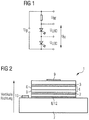
- the in the FIG. 1 illustrated block diagram comprises a voltage source, a resistor and an LED semiconductor body with two active layers.
- the voltage source supplies an operating voltage U B , which is preferably a DC voltage.
- an LED semiconductor body is connected, the active layers have a forward voltage U LED .
- radiation is generated in the two active layers, which are arranged in the forward direction, which is indicated by arrows.
- the number of active layers is adapted to the operating voltage U B in such a way that a voltage Uw dropping across the series resistor is at most as great as a voltage U H dropping across the LED semiconductor body.
- the inventive LED semiconductor body advantageously a higher efficiency than the conventional LED semiconductor body.
- the block diagram of the underlying LED semiconductor body can, as in FIG. 2 be formed represented.
- the LED semiconductor body 1 according to FIG. 2 has a first radiation-generating active layer 2 and a second radiation-generating active layer 3, wherein the active layers 2, 3 are arranged one above the other in the vertical direction, that is perpendicular to a main extension direction of the active layers.
- a tunnel junction 4 is formed, which is formed by means of a first semiconductor layer 5 of a first conductivity type, for example an n-type semiconductor layer, and a second semiconductor layer 6 of a second conductivity type, for example a p-type semiconductor layer.
- these two semiconductor layers 5, 6 are highly doped, so that an efficient tunnel junction with a low electrical contact resistance arises during operation.
- the active layers 2, 3 are arranged in the same direction, that is to say their pn junctions form a pn-pn or np-np structure. By means of the tunnel junction 4, the active layers 2, 3 are connected in series.
- the total forward voltage U LED is increased compared to a conventional LED semiconductor body with only one active layer. Furthermore, the voltage Uw dropping across the series resistor 10 is lower, as a result of which the radiation available for generating the radiation electrical energy is increased with advantage. Since the dimensions of the LED semiconductor body 1 with respect to the conventional LED semiconductor body change only insignificantly and in particular the cross section of the LED semiconductor body 1 is independent of the number of active layers, in addition to the amount of radiation and the radiation density is advantageously increased.
- the semiconductor body 1 is arranged on a carrier element 7.
- a surface of the semiconductor body 1 facing the carrier element 7 is preferably provided with a reflection layer 8 for reflecting the radiation generated by the active layers 2, 3 in the vertical direction.
- the reflection layer 8 at the same time forms a first outer contact 12 for the LED semiconductor body 1.
- a second outer contact 9 can be formed on a side of the LED semiconductor body 1 opposite the carrier element 7, in particular a second outer contact 9 can be formed.
- a vertically conductive component is formed, which is characterized by a comparatively homogeneous current distribution within the LED semiconductor body 1.
- the dropping resistor 10 is arranged on the carrier element 7.
- This arrangement is technically useful because, according to the invention, the voltage Uw dropping across the series resistor 10 is comparatively low and thus also the resulting heat loss is comparatively low. This reduces the risk of thermal disturbances or damage.
- the common arrangement of the LED semiconductor body 1 and the series resistor 10 on the carrier element 7 advantageously allows a comparatively high integration density.
- the LED semiconductor body 1 is in particular grown on a separate growth substrate and subsequently mounted on the carrier element 7, for example by means of soldering, bonding or gluing, wherein preferably the growth substrate is detached from the LED semiconductor body 1.
- the LED semiconductor body 1 is a thin-film semiconductor body.
- the active layers 2, 3 emit radiation of the same wavelength, the vertical direction indicating the main emission direction.
- the in FIG. 3 illustrated LED semiconductor body 1 comprises for an electrical connection, the first outer contact 12, which is arranged for example on the rear side, and the second outer contact 9, which is arranged for example on the front side.
- a first operating voltage U B can be applied to the LED semiconductor body 1.
- the LED semiconductor body 1 has an inner contact 11, which is arranged between the first active layer 2 and the second active layer 3.
- a second operating voltage U B can be applied to the LED semiconductor body 1.
- the second operating voltage is less than the first operating voltage.
- the LED semiconductor body 1 can therefore be operated by means of different operating voltages.
- a plurality of active layers can be arranged between the first outer contact 12 and the inner contact 11 and between the second outer contact 12 and the inner contact 11.
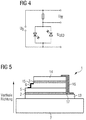
- the in the FIG. 4 illustrated block diagram comprises a voltage source, a resistor and an LED semiconductor body with two active layers.
- the voltage source supplies an operating voltage U B , which is preferably an alternating voltage.
- an LED semiconductor body is connected, the active layers have a forward voltage U LED . Since the two active layers are connected in antiparallel, they generate alternately radiation in the case of an alternating voltage.
- the number of active layers is adapted to the operating voltage U B in such a way that the voltage Uw dropping across the series resistor is at most equal to the voltage U H dropping across the LED semiconductor body.
- the voltage U H falling across the LED semiconductor body in this arrangement corresponds to the respective forward biased forward voltage U LED .
- the LED semiconductor body can be used as a replacement for a light bulb.
- the block diagram of the underlying LED semiconductor body can, as in FIG. 5 be formed represented.
- the LED semiconductor body 1 has a first radiation-generating active layer 2 and a second radiation-generating active layer 3, wherein the active layers 2, 3 are arranged one above the other in the vertical direction, that is perpendicular to a main extension direction of the active layers. Between the active layers 2, 3, a first semiconductor layer 5 of a first conductivity type, for example an n-type semiconductor layer, and a second semiconductor layer 6 of a second conductivity type, for example a p-type semiconductor layer, are arranged. On the rear side, the LED semiconductor body 1 is bounded by a first outer semiconductor layer 13 of the second conductivity type and on the front side by a second outer semiconductor layer 14 of the first conductivity type.
- the active layers 2, 3 are arranged in the same direction, that is to say their pn junctions form a pn-pn or np-np structure.
- the semiconductor layer 5 is electrically conductively connected to the semiconductor layer 6 by means of a first connection layer 15.
- the connection layer 15 is connected to a first electrical contact.
- the semiconductor layer 13 is electrically conductively connected to the semiconductor layer 14 by means of a second connection layer 16.
- the connection layer 16 is connected to a second electrical contact.
- the connection layer 16 is arranged on an electrical insulating layer 17.
- the semiconductor body 1 is arranged on a carrier element 7.
- the LED semiconductor body according to the invention is not limited to the embodiment in which the active layers are monolithically integrated. Rather, the LED semiconductor body according to the invention may also be formed from individual interconnected layer stacks, each having at least one active layer.
Landscapes
- Engineering & Computer Science (AREA)
- Microelectronics & Electronic Packaging (AREA)
- Computer Hardware Design (AREA)
- Power Engineering (AREA)
- Physics & Mathematics (AREA)
- Condensed Matter Physics & Semiconductors (AREA)
- General Physics & Mathematics (AREA)
- Led Devices (AREA)
Applications Claiming Priority (2)
| Application Number | Priority Date | Filing Date | Title |
|---|---|---|---|
| DE102006046038A DE102006046038A1 (de) | 2006-09-28 | 2006-09-28 | LED-Halbleiterkörper und Verwendung eines LED-Halbleiterkörpers |
| PCT/DE2007/001693 WO2008040300A1 (de) | 2006-09-28 | 2007-09-19 | Led-halbleiterkörper und verwendung eines led-halbleiterkörpers |
Publications (2)
| Publication Number | Publication Date |
|---|---|
| EP2062296A1 EP2062296A1 (de) | 2009-05-27 |
| EP2062296B1 true EP2062296B1 (de) | 2017-07-05 |
Family
ID=39118340
Family Applications (1)
| Application Number | Title | Priority Date | Filing Date |
|---|---|---|---|
| EP07817544.5A Not-in-force EP2062296B1 (de) | 2006-09-28 | 2007-09-19 | Led-halbleiterkörper und verwendung eines led-halbleiterkörpers |
Country Status (8)
Families Citing this family (23)
| Publication number | Priority date | Publication date | Assignee | Title |
|---|---|---|---|---|
| DE102008025160A1 (de) | 2008-05-26 | 2009-12-03 | Osram Opto Semiconductors Gmbh | Projektor für kleinste Projektionsflächen und Verwendung einer Mehrfarben-LED in einem Projektor |
| KR101332794B1 (ko) * | 2008-08-05 | 2013-11-25 | 삼성전자주식회사 | 발광 장치, 이를 포함하는 발광 시스템, 상기 발광 장치 및발광 시스템의 제조 방법 |
| DE102008053731B4 (de) * | 2008-10-29 | 2024-10-31 | OSRAM Opto Semiconductors Gesellschaft mit beschränkter Haftung | Optoelektronischer Halbleiterchip |
| US7983317B2 (en) * | 2008-12-16 | 2011-07-19 | Corning Incorporated | MQW laser structure comprising plural MQW regions |
| DE102010023342A1 (de) | 2010-06-10 | 2011-12-15 | Osram Opto Semiconductors Gmbh | Leuchtdiodenanordnung und Leuchtmittel insbesondere mit solch einer Leuchtdiodenanordnung |
| CN101902856A (zh) * | 2010-07-05 | 2010-12-01 | 陆敬仁 | 又一种用交流电直接驱动普通led的方法 |
| US9490239B2 (en) * | 2011-08-31 | 2016-11-08 | Micron Technology, Inc. | Solid state transducers with state detection, and associated systems and methods |
| US8809897B2 (en) | 2011-08-31 | 2014-08-19 | Micron Technology, Inc. | Solid state transducer devices, including devices having integrated electrostatic discharge protection, and associated systems and methods |
| US9070613B2 (en) * | 2011-09-07 | 2015-06-30 | Lg Innotek Co., Ltd. | Light emitting device |
| EP2618388B1 (en) * | 2012-01-20 | 2019-10-02 | OSRAM Opto Semiconductors GmbH | Light-emitting diode chip |
| TWI470826B (zh) * | 2012-03-30 | 2015-01-21 | Phostek Inc | 發光二極體裝置 |
| JP6071650B2 (ja) * | 2013-03-01 | 2017-02-01 | スタンレー電気株式会社 | 半導体発光装置 |
| US9825088B2 (en) * | 2015-07-24 | 2017-11-21 | Epistar Corporation | Light-emitting device and manufacturing method thereof |
| US10784398B2 (en) | 2015-12-24 | 2020-09-22 | Vuereal Inc. | Vertical solid state devices |
| US9859470B2 (en) | 2016-03-10 | 2018-01-02 | Epistar Corporation | Light-emitting device with adjusting element |
| US20180287027A1 (en) | 2017-03-30 | 2018-10-04 | Vuereal Inc. | Vertical solid-state devices |
| US11721784B2 (en) | 2017-03-30 | 2023-08-08 | Vuereal Inc. | High efficient micro devices |
| US11600743B2 (en) | 2017-03-30 | 2023-03-07 | Vuereal Inc. | High efficient microdevices |
| JP7323783B2 (ja) | 2019-07-19 | 2023-08-09 | 日亜化学工業株式会社 | 発光装置の製造方法及び発光装置 |
| DE102020001353B3 (de) * | 2020-03-03 | 2020-12-31 | Azur Space Solar Power Gmbh | Stapelförmiges photonisches lll-V-Halbleiterbauelement und Optokoppler |
| US11489089B2 (en) | 2020-06-19 | 2022-11-01 | Lextar Electronics Corporation | Light emitting device with two vertically-stacked light emitting cells |
| WO2022178393A1 (en) * | 2021-02-22 | 2022-08-25 | The Regents Of The University Of California | Monolithic, cascaded, multiple color light-emitting diodes with independent junction control |
| CN117438516A (zh) * | 2023-12-21 | 2024-01-23 | 江西兆驰半导体有限公司 | 一种垂直结构高压Micro LED芯片及其制备方法 |
Family Cites Families (24)
| Publication number | Priority date | Publication date | Assignee | Title |
|---|---|---|---|---|
| DE2323971C2 (de) | 1973-05-11 | 1982-05-27 | Siemens AG, 1000 Berlin und 8000 München | Bauelement mit Lumineszenzdiode |
| DE2342298A1 (de) * | 1973-08-22 | 1975-02-27 | Licentia Gmbh | Mehrfach-leuchtdiode |
| GB1485462A (en) * | 1975-01-09 | 1977-09-14 | Thorn Electrical Ind Ltd | High voltage semi-conductor lamps |
| DD219086A3 (de) * | 1982-01-04 | 1985-02-20 | Karl Marx Stadt Tech Hochschul | Wechselspannungsangesteuerte lumineszenzdioden |
| US4939426A (en) * | 1987-03-19 | 1990-07-03 | United States Of America | Light emitting diode array |
| DE3929477A1 (de) * | 1989-09-05 | 1991-03-07 | Siemens Ag | Led-anordnung |
| JP2549205B2 (ja) * | 1990-12-26 | 1996-10-30 | ローム株式会社 | Ledアレイ光源 |
| JP3352840B2 (ja) * | 1994-03-14 | 2002-12-03 | 株式会社東芝 | 逆並列接続型双方向性半導体スイッチ |
| DE9404982U1 (de) * | 1994-03-23 | 1994-06-01 | Siemens AG, 80333 München | Leuchtdiode mit hohem Wirkungsgrad |
| JP2000244020A (ja) * | 1999-02-23 | 2000-09-08 | Matsushita Electric Works Ltd | 光源装置 |
| US6885035B2 (en) * | 1999-12-22 | 2005-04-26 | Lumileds Lighting U.S., Llc | Multi-chip semiconductor LED assembly |
| US6323598B1 (en) | 2000-09-29 | 2001-11-27 | Aerospace Optics, Inc. | Enhanced trim resolution voltage-controlled dimming led driver |
| US6547249B2 (en) * | 2001-03-29 | 2003-04-15 | Lumileds Lighting U.S., Llc | Monolithic series/parallel led arrays formed on highly resistive substrates |
| US7135711B2 (en) * | 2001-08-30 | 2006-11-14 | Osram Opto Semiconductors Gmbh | Electroluminescent body |
| US6822991B2 (en) * | 2002-09-30 | 2004-11-23 | Lumileds Lighting U.S., Llc | Light emitting devices including tunnel junctions |
| JP4072632B2 (ja) * | 2002-11-29 | 2008-04-09 | 豊田合成株式会社 | 発光装置及び発光方法 |
| TW591811B (en) * | 2003-01-02 | 2004-06-11 | Epitech Technology Corp Ltd | Color mixing light emitting diode |
| CN1275337C (zh) * | 2003-09-17 | 2006-09-13 | 北京工大智源科技发展有限公司 | 高效高亮度多有源区隧道再生白光发光二极管 |
| DE102004004765A1 (de) * | 2004-01-29 | 2005-09-01 | Rwe Space Solar Power Gmbh | Aktive Zonen aufweisende Halbleiterstruktur |
| JP2005229037A (ja) | 2004-02-16 | 2005-08-25 | Kankyo Shomei:Kk | 発光ダイオード点灯回路 |
| CN101685823B (zh) | 2004-02-20 | 2012-04-18 | 奥斯兰姆奥普托半导体有限责任公司 | 光电组件及其制造方法以及具有多个光电组件的装置 |
| JP3802911B2 (ja) | 2004-09-13 | 2006-08-02 | ローム株式会社 | 半導体発光装置 |
| US7095052B2 (en) * | 2004-10-22 | 2006-08-22 | Avago Technologies Ecbu Ip (Singapore) Pte. Ltd. | Method and structure for improved LED light output |
| EP2259318A3 (en) * | 2005-02-04 | 2014-01-08 | Seoul Opto Device Co., Ltd. | Light emitting device having a plurality of light emitting cells and method of fabricating the same |
-
2006
- 2006-09-28 DE DE102006046038A patent/DE102006046038A1/de not_active Withdrawn
-
2007
- 2007-09-19 WO PCT/DE2007/001693 patent/WO2008040300A1/de active Application Filing
- 2007-09-19 EP EP07817544.5A patent/EP2062296B1/de not_active Not-in-force
- 2007-09-19 US US12/443,155 patent/US8283684B2/en not_active Expired - Fee Related
- 2007-09-19 JP JP2009529522A patent/JP5479098B2/ja not_active Expired - Fee Related
- 2007-09-19 CN CN200780035954.4A patent/CN101563778B/zh not_active Expired - Fee Related
- 2007-09-19 KR KR1020097008601A patent/KR101421761B1/ko not_active Expired - Fee Related
- 2007-09-27 TW TW096135846A patent/TWI384644B/zh not_active IP Right Cessation
Non-Patent Citations (1)
| Title |
|---|
| None * |
Also Published As
| Publication number | Publication date |
|---|---|
| US20110240955A1 (en) | 2011-10-06 |
| TW200826326A (en) | 2008-06-16 |
| WO2008040300A1 (de) | 2008-04-10 |
| KR101421761B1 (ko) | 2014-07-22 |
| CN101563778A (zh) | 2009-10-21 |
| TWI384644B (zh) | 2013-02-01 |
| JP2010505251A (ja) | 2010-02-18 |
| DE102006046038A1 (de) | 2008-04-03 |
| US8283684B2 (en) | 2012-10-09 |
| EP2062296A1 (de) | 2009-05-27 |
| JP5479098B2 (ja) | 2014-04-23 |
| CN101563778B (zh) | 2014-07-09 |
| KR20090064469A (ko) | 2009-06-18 |
Similar Documents
| Publication | Publication Date | Title |
|---|---|---|
| EP2062296B1 (de) | Led-halbleiterkörper und verwendung eines led-halbleiterkörpers | |
| EP1966836B1 (de) | Led-halbleiterkörper und verwendung eines led-halbleiterkörpers | |
| DE102006051745B4 (de) | LED-Halbleiterkörper und Verwendung eines LED-Halbleiterkörpers | |
| EP2245667B1 (de) | Monolithischer, optoelektronischer halbleiterkörper und verfahren zur herstellung eines solchen | |
| EP2499668B1 (de) | Dünnfilm-halbleiterbauelement mit schutzdiodenstruktur und verfahren zur herstellung eines dünnfilm-halbleiterbauelements | |
| DE102011116232B4 (de) | Optoelektronischer Halbleiterchip und Verfahren zu dessen Herstellung | |
| EP2149159B1 (de) | Optoelektronischer halbleiterkörper und verfahren zur herstellung eines solchen | |
| EP2553726B1 (de) | Optoelektronischer halbleiterchip | |
| EP2208240B1 (de) | Optoelektronischer halbleiterchip mit einer mehrfachquantentopfstruktur | |
| EP2519980B1 (de) | Lichtemittierender halbleiterchip | |
| DE202009018090U1 (de) | Halbleiter-Lichtemittervorrichtung | |
| DE112016004262T5 (de) | Selbstausrichtender freischwebender Spiegel für Durchkontaktierungen | |
| EP3206238B1 (de) | Lichtemittierende dünnfilm-diode mit einer spiegelschicht und verfahren zu deren herstellung | |
| DE102008051050A1 (de) | Modul mit optoelektronischen Halbleiterelementen | |
| DE102008051048A1 (de) | Optoelektronischer Halbleiterkörper | |
| WO2013034485A1 (de) | Optoelektronisches bauelement | |
| DE10322705B4 (de) | Herstellverfahren für eine LED mit dicker Epitaxieschicht auf III-V-Halbleiterbasis und derartige LED | |
| DE102008039790B4 (de) | Optoelektronisches Bauelement und Verfahren zu dessen Herstellung | |
| WO2008040274A1 (de) | Led-halbleiterkörper und verwendung eines led-halbleiterkörpers | |
| DE102012105772A1 (de) | Halbleiter-Leuchtdiodenvorrichtungs-Verpackung | |
| DE102015104700A1 (de) | Optoelektronischer Halbleiterchip | |
| EP2304816B1 (de) | Elektrolumineszierende vorrichtung und verfahren zur herstellung einer elektrolumineszierenden vorrichtung | |
| WO2016166154A1 (de) | Strahlungsemittierendes halbleiterbauelement | |
| DE102009054555A1 (de) | Optoelektronischer Halbleiterchip und Verfahren zum Herstellen eines optoelektronischen Halbleiterchips | |
| WO2013034486A1 (de) | Optoelektronisches bauelement |
Legal Events
| Date | Code | Title | Description |
|---|---|---|---|
| PUAI | Public reference made under article 153(3) epc to a published international application that has entered the european phase |
Free format text: ORIGINAL CODE: 0009012 |
|
| 17P | Request for examination filed |
Effective date: 20090324 |
|
| AK | Designated contracting states |
Kind code of ref document: A1 Designated state(s): AT BE BG CH CY CZ DE DK EE ES FI FR GB GR HU IE IS IT LI LT LU LV MC MT NL PL PT RO SE SI SK TR |
|
| AX | Request for extension of the european patent |
Extension state: AL BA HR MK RS |
|
| DAX | Request for extension of the european patent (deleted) | ||
| RBV | Designated contracting states (corrected) |
Designated state(s): DE FR GB |
|
| 17Q | First examination report despatched |
Effective date: 20140602 |
|
| GRAP | Despatch of communication of intention to grant a patent |
Free format text: ORIGINAL CODE: EPIDOSNIGR1 |
|
| INTG | Intention to grant announced |
Effective date: 20170217 |
|
| GRAS | Grant fee paid |
Free format text: ORIGINAL CODE: EPIDOSNIGR3 |
|
| GRAA | (expected) grant |
Free format text: ORIGINAL CODE: 0009210 |
|
| AK | Designated contracting states |
Kind code of ref document: B1 Designated state(s): DE FR GB |
|
| REG | Reference to a national code |
Ref country code: GB Ref legal event code: FG4D Free format text: NOT ENGLISH |
|
| REG | Reference to a national code |
Ref country code: DE Ref legal event code: R096 Ref document number: 502007015737 Country of ref document: DE |
|
| REG | Reference to a national code |
Ref country code: DE Ref legal event code: R097 Ref document number: 502007015737 Country of ref document: DE |
|
| PLBE | No opposition filed within time limit |
Free format text: ORIGINAL CODE: 0009261 |
|
| STAA | Information on the status of an ep patent application or granted ep patent |
Free format text: STATUS: NO OPPOSITION FILED WITHIN TIME LIMIT |
|
| 26N | No opposition filed |
Effective date: 20180406 |
|
| GBPC | Gb: european patent ceased through non-payment of renewal fee |
Effective date: 20171005 |
|
| REG | Reference to a national code |
Ref country code: FR Ref legal event code: ST Effective date: 20180531 |
|
| PG25 | Lapsed in a contracting state [announced via postgrant information from national office to epo] |
Ref country code: GB Free format text: LAPSE BECAUSE OF NON-PAYMENT OF DUE FEES Effective date: 20171005 |
|
| PG25 | Lapsed in a contracting state [announced via postgrant information from national office to epo] |
Ref country code: FR Free format text: LAPSE BECAUSE OF NON-PAYMENT OF DUE FEES Effective date: 20171002 |
|
| PGFP | Annual fee paid to national office [announced via postgrant information from national office to epo] |
Ref country code: DE Payment date: 20210920 Year of fee payment: 15 |
|
| REG | Reference to a national code |
Ref country code: DE Ref legal event code: R119 Ref document number: 502007015737 Country of ref document: DE |
|
| PG25 | Lapsed in a contracting state [announced via postgrant information from national office to epo] |
Ref country code: DE Free format text: LAPSE BECAUSE OF NON-PAYMENT OF DUE FEES Effective date: 20230401 |
|
| P01 | Opt-out of the competence of the unified patent court (upc) registered |
Effective date: 20230825 |