EP2061095A1 - Light-emitting device - Google Patents
Light-emitting device Download PDFInfo
- Publication number
- EP2061095A1 EP2061095A1 EP07806388A EP07806388A EP2061095A1 EP 2061095 A1 EP2061095 A1 EP 2061095A1 EP 07806388 A EP07806388 A EP 07806388A EP 07806388 A EP07806388 A EP 07806388A EP 2061095 A1 EP2061095 A1 EP 2061095A1
- Authority
- EP
- European Patent Office
- Prior art keywords
- light
- emitting chip
- optical member
- emitting device
- emitting
- Prior art date
- Legal status (The legal status is an assumption and is not a legal conclusion. Google has not performed a legal analysis and makes no representation as to the accuracy of the status listed.)
- Withdrawn
Links
Images





Classifications
-
- H—ELECTRICITY
- H10—SEMICONDUCTOR DEVICES; ELECTRIC SOLID-STATE DEVICES NOT OTHERWISE PROVIDED FOR
- H10H—INORGANIC LIGHT-EMITTING SEMICONDUCTOR DEVICES HAVING POTENTIAL BARRIERS
- H10H20/00—Individual inorganic light-emitting semiconductor devices having potential barriers, e.g. light-emitting diodes [LED]
- H10H20/80—Constructional details
- H10H20/85—Packages
- H10H20/855—Optical field-shaping means, e.g. lenses
-
- H—ELECTRICITY
- H10—SEMICONDUCTOR DEVICES; ELECTRIC SOLID-STATE DEVICES NOT OTHERWISE PROVIDED FOR
- H10H—INORGANIC LIGHT-EMITTING SEMICONDUCTOR DEVICES HAVING POTENTIAL BARRIERS
- H10H20/00—Individual inorganic light-emitting semiconductor devices having potential barriers, e.g. light-emitting diodes [LED]
- H10H20/80—Constructional details
- H10H20/85—Packages
- H10H20/851—Wavelength conversion means
- H10H20/8515—Wavelength conversion means not being in contact with the bodies
-
- H—ELECTRICITY
- H10—SEMICONDUCTOR DEVICES; ELECTRIC SOLID-STATE DEVICES NOT OTHERWISE PROVIDED FOR
- H10H—INORGANIC LIGHT-EMITTING SEMICONDUCTOR DEVICES HAVING POTENTIAL BARRIERS
- H10H20/00—Individual inorganic light-emitting semiconductor devices having potential barriers, e.g. light-emitting diodes [LED]
- H10H20/80—Constructional details
- H10H20/85—Packages
- H10H20/852—Encapsulations
- H10H20/853—Encapsulations characterised by their shape
-
- H—ELECTRICITY
- H10—SEMICONDUCTOR DEVICES; ELECTRIC SOLID-STATE DEVICES NOT OTHERWISE PROVIDED FOR
- H10W—GENERIC PACKAGES, INTERCONNECTIONS, CONNECTORS OR OTHER CONSTRUCTIONAL DETAILS OF DEVICES COVERED BY CLASS H10
- H10W72/00—Interconnections or connectors in packages
- H10W72/20—Bump connectors, e.g. solder bumps or copper pillars; Dummy bumps; Thermal bumps
Definitions
- the present invention relates to a light-emitting device having a light-emitting chip such as a light-emitting diode.
- the light-emitting device is used for a lighting fixture, for example.
- the light-emitting device has a light emitter for converting a wavelength of a light emitted from the light-emitting chip.
- the light emitter includes a fluorescent material which is excited by the light emitted from the light-emitting chip.
- a light-emitting device includes a base, a light-emitting chip mounted on the base, and a light emitter disposed above the light-emitting chip.
- the light-emitting chip includes a semiconductor material and generates a first light.
- the light emitter has a sheet-like shape and includes a fluorescent material excited by the first light to emit a second light.
- the light-emitting device further includes an optical member contacting side surfaces of the light-emitting chip and including a transparent material. The optical member has an opening in which is disposed the light-emitting chip and a flat upper surface opposed to the light emitter.
- a light-emitting device includes a base, a light-emitting chip mounted on the base, and a light emitter disposed above the light-emitting chip.
- the light-emitting chip includes a semiconductor material and generates a first light.
- the light emitter has a sheet-like shape and includes a fluorescent material excited by the first light to emit a second light.
- the light-emitting device further includes an optical member disposed between the light-emitting chip and the light emitter and including a transparent material. The optical member has a flat upper surface opposed to the light emitter.
- the light-emitting device in accordance with one embodiment of the invention includes the optical member which has the flat upper surface opposed to the light emitter and contacts with the side surfaces of the light-emitting chip. In this construction, the deviation of light emission distribution can be reduced.
- the light-emitting device in accordance with another embodiment of the invention includes the optical member which has the flat upper surface opposed to the light emitter and is disposed between the light-emitting chip and the light emitter. In this construction, the deviation of light emission distribution can be reduced.
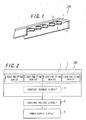
- an illuminating apparatus 100 includes a substrate 1, a plurality of light-emitting devices 2 mounted on the substrate 1, and a light-reflecting member 3.
- the substrate 1 has a conductor pattern 1a.
- a plurality of the light-emitting devices 2 are electrically connected to the conductor pattern 1a.
- the light-reflecting member 3 is placed at a location where it can be reached by at least part of light emitted from a plurality of the light-emitting devices 2.
- the light-reflecting member 3 is disposed beside a plurality of the light-emitting devices 2. Referring to Fig.
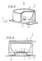
- the illuminating apparatus 100 comprises a plurality of the light-emitting devices 2 disposed on the substrate 1 and a constant current circuit 4.
- a constant voltage circuit 5 is electrically connected to the constant current circuit 4 of the illuminating apparatus 100.
- a power supply circuit 6 is electrically connected to the constant current circuit 5.
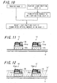
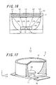
- the light-emitting device 2 includes a base 11, a light-emitting chip 12 mounted on the base 11, and a light emitter (wavelength converter) 13 disposed above the light-emitting chip 12.
- the light-emitting device 2 further includes an optical member 14 contacting with the light-emitting chip 12.
- the base 11 is made of an insulating material.
- the base 11 has a conductive pattern 15.
- a lead terminal 16 is electrically connected to the conductive pattern 15 and disposed at a mounting surface M of the light-emitting device 2.
- the light-emitting chip 12 is a light-emitting diode which generates a first light.
- the first light has at least part of wavelength range from 370 nm to 400 nm (ultraviolet) or at least part of wavelength range from 450 nm to 500 nm (blue).
- the light-emitting chip 12 includes a first semiconductor layer (n-type semiconductor layer) 12n stacked on a substrate 12b, a semiconductor active layer 12a, and a second semiconductor layer (p-type semiconductor layer) 12p.
- the n-type semiconductor layer 12n, the semiconductor active layer 12a, and the p-type semiconductor layer 12p are made of gallium nitride (GaN).
- the light-emitting chip 12 includes a first electrode pad (n-side electrode pad) 12np disposed on the n-type semiconductor layer 12n and a second electrode pad (p-side electrode pad) 12pp disposed on the p-type semiconductor layer 12p.
- the light-emitting chip 12 further includes a metal contact member 19 disposed on the n-side electrode pad 12np.
- the n-side electrode pad 12np and the p-side electrode pad 12pp are each electrically connected, via solder 20, to the conductive pattern 15 disposed on the base 11.
- the light-emitting chip 12 is mounted on the base 11 by flip-chip bonding. That is, the light-emitting chip 12 is mounted on the base 11, with the mounting surface M having the n-side electrode pad 12np and the p-side electrode pad 12pp opposed to the base 11.
- the wavelength converter 13 is apart from the light-emitting chip 12 and has a sheet-like shape.
- the wavelength converter 13 includes a fluorescent.material 17 which is excited by the first light to emit a second light.
- the second light' has a second wavelength which differs from a first wavelength of the first light.
- the fluorescent material 17 emits light having at least part of wavelength range from 625 nm to 740 nm (red), light having at least part of wavelength range from 520 nm to 565 nm (green), and light having at least part of wavelength range from 450 nm to 500 nm (blue).
- the light-emitting device 2 emits a mixed light (white light) of red light, green light, and blue light emitted from the wavelength converter 13.
- the fluorescent material 17 emits light having at least part of wavelength range from 565 nm to 590 nm (yellow).
- the light-emitting device 2 emits a mixed light (white light) of blue light emitted from the light-emitting chip and yellow light emitted from the wavelength converter 13.
- the fluorescent material 17 emits light having at least part of wavelength range from 625 nm to 740.nm (red) and light having at'least part of wavelength range from 520 nm to 565 nm (green).
- the light-emitting device 2 emits a mixed light (white light) of blue light emitted from the light-emitting chip 12, and red light and green light emitted from the wavelength converter 13.
- the wavelength converter 13 further includes a resin material 18 containing the fluorescent material 17.
- the resin material 18 is silicone resin which exhibits transparency.
- the optical member 14 covers the active layer 12a of the light-emitting chip 12. As illustrated'in Fig. 6 , the optical member 14 contacts with side surfaces 12s of the light-emitting chip 12.
- the light-emitting chip 12 is mounted on an xy plane in a virtual xyz space.
- the optical member 14 has a flat upper surface 14u opposed to the wavelength converter 13.
- the optical member 14 has an opening 14p in which is disposed the light-emitting chip 12.
- the optical member 14 includes a transparent material.
- the transparent material is resin or glass.
- the optical member 14 contacts at least with the side surface 12s located nearest the p-side electrode pad 12p. Referring to Figs.
- the structure of the light-emitting chip 12 will be described in further detail.
- the n-type semiconductor layer 12n is exposed from the p-type semiconductor layer 12p as seen at the side of the mounting surface M.
- the optical member 14 is formed at least on a side surface 12sn located nearest the n-side electrode pad 12np.
- the n-type semiconductor layer 12n is exposed from the p-type semiconductor layer 12p as seen at the corner of the mounting surface M.
- the optical member 14 is formed at least.on the side surface 12sn located nearest the n-side electrode pad 12np. As illustrated in Fig. 6 , the optical member 14 surrounds the side surfaces 12s of the light-emitting chip 12.
- the first light L1a emitted from the light-emitting chip 12 travels upward and sideward from the light-emitting chip 12.
- the first light L1a now traveling sideways in relation to the light-emitting chip 12, travels further from the.flat upper surface 14u of the optical member 14 toward the wavelength converter 13.
- the light radiated from the upper surface 14u is indicated by a symbol L1b.
- the first light L1a and L1b is subjected to wavelength conversion by the fluorescent material 17 of the wavelength converter 13.
- the second light L2 radiated from the fluorescent material travels in a light-exiting direction.D in which light exits from the light-emitting device 2.
- the deviation of the irradiation distribution of the first light L1a and L1b with respect to the wavelength converter 13 can be reduced.
- the method for manufacturing the light-emitting devices 2 includes the following steps A through D:
- the light-emitting chip 12 has the mounting surface M fitted with the first electrode pad (n-side electrode pad) 12np and the second electrode pad (p-side electrode pad) 12pp.
- the optical member 14 is formed on the side surfaces 12s of the light-emitting chip 12.
- the optical member 14 is formed at least on the side surface 12sn located nearest the n-side electrode pad 12np. Step C will be described in further detail.
- a plurality of the light-emitting chips 12 are arranged on an adhesive film 4.
- the adhesive film 4 is adhered to the substrate 12b of the light-emitting chip 12.
- the light-emitting chip 12 includes the metal contact member 19 formed on the n-side electrode 12np.
- a transparent material 14' in a molten state is admitted onto the adhesive film 4 so as to find its way into a region between the two or more light-emitting chips 12.
- the transparent material 14' covers the active layer 12a of the light-emitting chip 12.
- the p-side electrode 12pp and the metal contact member 19 of the light-emitting chip 12 are exposed from the transparent material 14'.
- the transparent material 14' is cured by process of heating or otherwise.
- the transparent material 14' in a cured state is cut off at a location between the two or more light-emitting chips 12.
- the adhesive film 4 is removed from the light-emitting chips 12 following the cutting of the transparent material 14'.
- the light-emitting chip 12 is mounted on the base 11 in a state as illustrated in Fig. 5 .
- the optical member 14 is formed on the side surfaces of the light-emitting chip 12. This makes it possible to reduce the tilt of the light-emitting chip 12 in mounting.
- the optical member 14 covers the active layer 12a of the light-emitting chip 12.
- the optical member 14 contacts with the side surface 12s and a top 12t of the light-emitting chip 12.
- the optical member 14 has the flat upper surface 14u opposed to the wavelength converter 13.
- the optical member 14 has the opening 14p in which is disposed the light-emitting chip 12.
- the optical member 14 contacts at least with the side surface 12s located nearest the p-side electrode pad 12p.
- the optical member 14 surrounds the side surfaces 12s and the top 12t of the light-emitting chip 12. Otherwise, this embodiment is structurally identical to the light-emitting device 2 illustrated in Fig. 3 . As illustrated in Fig.
- first light L1a emitted from the light-emitting chip 12 travels upward and sideward from the light-emitting chip 12.
- the first light L1a travels from the flat upper surface 14u of the optical member 14 toward the wavelength converter 13.
- the light radiated from the upper surface 14u is indicated by a symbol L1b.
- the deviation of the irradiation distribution of the first light L1b with respect to the wavelength converter 13 can be reduced.
- the light-emitting device 2 has an optical member 24 including a transparent material.
- transparent refers to a property that allows light having at least part of the wavelengths of light generated by the light-emitting chip 12 to pass.
- the transparent material is glass or resin.
- the optical member 24 has a flat upper surface 24u opposed to the wavelength converter 13. The optical member 24 is placed between the light-emitting chip 12 and the wavelength converter 13. The upper surface 24u of the optical member 24 is apart from the wavelength converter 13.
- the light-emitting device 2 further includes a transparent resin 20 which surrounds the side surfaces and the top of the light-emitting chip 12. The transparent resin 20 is adhered to the optical member 24.
- this embodiment is structurally identical to the light-emitting device 2 illustrated in Fig. 3 .
- first light L1a emitted from the light-emitting chip 12 passes through the transparent resin 20 and is then radiated from the flat upper surface 24u of the optical member 24.
- the light radiated from the upper surface 24u is indicated by a symbol L1b.
- the deviation of the irradiation distribution of the first light L1b with respect to the wavelength converter 13 can be reduced.
- the upper surface 24u of the optical member 24 contacts with the wavelength converter 13. Otherwise, this embodiment is structurally identical to the light-emitting device 2 illustrated in Fig. 18 .
- first light L1a emitted from the light-emitting chip 12 passes through the transparent resin 20 and is then radiated from the flat upper surface 24u of the optical member 24.
- the light radiated from the upper surface 24u is indicated by a symbol L1b.
- the deviation of the irradiation distribution of the first light L1b with respect to the wavelength converter 13 can be reduced.
Landscapes
- Led Device Packages (AREA)
Abstract
Description
- The present invention relates to a light-emitting device having a light-emitting chip such as a light-emitting diode.
- In recent years, developments directed toward producing a light-emitting device having a light-emitting chip such as a light-emitting diode have been under way. The light-emitting device is used for a lighting fixture, for example. The light-emitting device has a light emitter for converting a wavelength of a light emitted from the light-emitting chip. The light emitter includes a fluorescent material which is excited by the light emitted from the light-emitting chip.
- In conventional light-emitting devices, there has been a demand for enhancement in the efficiency of wavelength conversion for light emanating from a light-emitting chip. In order to increase the efficiency of wavelength conversion, it is necessary to reduce the proportion of that part of light emitted from a light-emitting chip which disappears on its way to a light emitter.
- According to one embodiment of the invention, a light-emitting device includes a base, a light-emitting chip mounted on the base, and a light emitter disposed above the light-emitting chip. The light-emitting chip includes a semiconductor material and generates a first light. The light emitter has a sheet-like shape and includes a fluorescent material excited by the first light to emit a second light. The light-emitting device further includes an optical member contacting side surfaces of the light-emitting chip and including a transparent material. The optical member has an opening in which is disposed the light-emitting chip and a flat upper surface opposed to the light emitter.
- According to another embodiment of the invention, a light-emitting device includes a base, a light-emitting chip mounted on the base, and a light emitter disposed above the light-emitting chip. The light-emitting chip includes a semiconductor material and generates a first light. The light emitter has a sheet-like shape and includes a fluorescent material excited by the first light to emit a second light. The light-emitting device further includes an optical member disposed between the light-emitting chip and the light emitter and including a transparent material. The optical member has a flat upper surface opposed to the light emitter.
- The light-emitting device in accordance with one embodiment of the invention includes the optical member which has the flat upper surface opposed to the light emitter and contacts with the side surfaces of the light-emitting chip. In this construction, the deviation of light emission distribution can be reduced.
- The light-emitting device in accordance with another embodiment of the invention includes the optical member which has the flat upper surface opposed to the light emitter and is disposed between the light-emitting chip and the light emitter. In this construction, the deviation of light emission distribution can be reduced.
-
-
Fig. 1 is a perspective view illustrating an embodiment of the illuminating apparatus of the invention. -
Fig. 2 is a view illustrating the circuit configuration of the illuminating apparatus. -
Fig. 3 is a perspective view illustrating an embodiment of the light-emitting device of the invention. -
Fig. 4 is.a sectional view of the light-emitting device illustrated inFig. 3 . -
Fig. 5 is an enlarged view of the light-emitting chip and the optical member illustrated inFig. 4 . -
Fig. 6 is an enlarged view of the light-emitting chip and the optical member illustrated inFig. 3 . -
Fig. 7 is a perspective view of the light-emitting chip. -
Fig. 8 is a perspective view of another light-emitting chip. -
Fig. 9 is a view illustrating how light travels in the light-emitting device illustrated inFig. 4 . -
Fig. 10 is a view illustrating the method for manufacturing the light-emitting device. -
Fig. 11 is a view illustrating the method for manufacturing the light-emitting device. -
Fig. 12 is a view illustrating the method for manufacturing the light-emitting device. -
Fig. 13 is a view illustrating the method for manufacturing the light-emitting device. -
Fig. 14 is a perspective view illustrating another embodiment of the light-emitting device of the invention. -
Fig. 15 is a sectional view of the light-emitting device illustrated inFig. 14 . -
Fig. 16 is a view illustrating how light travels in the light-emitting device of another embodiment. -
Fig. 17 is a perspective view illustrating still another embodiment of the light-emitting device of the invention. -
Fig. 18 is a sectional view of the light-emitting device illustrated inFig. 17 . -
Fig. 19 is a view illustrating how light travels in the light-emitting device illustrated inFig. 18 . -
Fig. 20 is a sectional view illustrating yet a further embodiment of the light-emitting device of the invention. -
Fig. 21 is a view illustrating how light travels in the light-emitting device illustrated inFig. 20 . - Hereinafter, the embodiments of the invention will be described in detail with reference to drawings. As illustrated in
Fig. 1 , anilluminating apparatus 100 includes asubstrate 1, a plurality of light-emittingdevices 2 mounted on thesubstrate 1, and a light-reflectingmember 3. Thesubstrate 1 has a conductor pattern 1a. A plurality of the light-emittingdevices 2 are electrically connected to the conductor pattern 1a. The light-reflectingmember 3 is placed at a location where it can be reached by at least part of light emitted from a plurality of the light-emittingdevices 2. InFig. 1 , the light-reflectingmember 3 is disposed beside a plurality of the light-emittingdevices 2. Referring toFig. 2 , the circuit configuration of theilluminating apparatus 100 will be described. Theilluminating apparatus 100 comprises a plurality of the light-emittingdevices 2 disposed on thesubstrate 1 and a constantcurrent circuit 4. Aconstant voltage circuit 5 is electrically connected to the constantcurrent circuit 4 of theilluminating apparatus 100. Apower supply circuit 6 is electrically connected to the constantcurrent circuit 5. - As illustrated in
Fig. 3 , the light-emitting device 2 includes abase 11, a light-emittingchip 12 mounted on thebase 11, and a light emitter (wavelength converter) 13 disposed above the light-emittingchip 12. The light-emitting device 2 further includes anoptical member 14 contacting with the light-emittingchip 12. Thebase 11 is made of an insulating material. As illustrated inFig. 4 , thebase 11 has aconductive pattern 15. Alead terminal 16 is electrically connected to theconductive pattern 15 and disposed at a mounting surface M of the light-emitting device 2. - The light-emitting
chip 12 is a light-emitting diode which generates a first light. The first light has at least part of wavelength range from 370 nm to 400 nm (ultraviolet) or at least part of wavelength range from 450 nm to 500 nm (blue). As illustrated inFig. 5 , the light-emittingchip 12 includes a first semiconductor layer (n-type semiconductor layer) 12n stacked on asubstrate 12b, a semiconductoractive layer 12a, and a second semiconductor layer (p-type semiconductor layer) 12p. The n-type semiconductor layer 12n, the semiconductoractive layer 12a, and the p-type semiconductor layer 12p are made of gallium nitride (GaN). As another example of the light-emittingchip 12, there is the one made of aluminum nitride (AlN). The light-emittingchip 12 includes a first electrode pad (n-side electrode pad) 12np disposed on the n-type semiconductor layer 12n and a second electrode pad (p-side electrode pad) 12pp disposed on the p-type semiconductor layer 12p. The light-emittingchip 12 further includes ametal contact member 19 disposed on the n-side electrode pad 12np. The n-side electrode pad 12np and the p-side electrode pad 12pp are each electrically connected, viasolder 20, to theconductive pattern 15 disposed on thebase 11. The light-emittingchip 12 is mounted on thebase 11 by flip-chip bonding. That is, the light-emittingchip 12 is mounted on thebase 11, with the mounting surface M having the n-side electrode pad 12np and the p-side electrode pad 12pp opposed to thebase 11. - The
wavelength converter 13 is apart from the light-emittingchip 12 and has a sheet-like shape. Thewavelength converter 13 includes afluorescent.material 17 which is excited by the first light to emit a second light. In this embodiment, the second light'has a second wavelength which differs from a first wavelength of the first light. In the light-emittingdevice 2 having the light-emittingchip 12 which generates ultraviolet light, thefluorescent material 17 emits light having at least part of wavelength range from 625 nm to 740 nm (red), light having at least part of wavelength range from 520 nm to 565 nm (green), and light having at least part of wavelength range from 450 nm to 500 nm (blue). The light-emittingdevice 2 emits a mixed light (white light) of red light, green light, and blue light emitted from thewavelength converter 13. In the light-emittingdevice 2 having the light-emittingchip 12 which generates blue light, thefluorescent material 17 emits light having at least part of wavelength range from 565 nm to 590 nm (yellow). The light-emittingdevice 2 emits a mixed light (white light) of blue light emitted from the light-emitting chip and yellow light emitted from thewavelength converter 13. - In another example of the light-emitting
device 2 having the light-emittingchip 12 which generates blue light, thefluorescent material 17 emits light having at least part of wavelength range from 625 nm to 740.nm (red) and light having at'least part of wavelength range from 520 nm to 565 nm (green). The light-emittingdevice 2 emits a mixed light (white light) of blue light emitted from the light-emittingchip 12, and red light and green light emitted from thewavelength converter 13. Thewavelength converter 13 further includes aresin material 18 containing thefluorescent material 17. Theresin material 18 is silicone resin which exhibits transparency. - As illustrated in
Fig. 5 , theoptical member 14 covers theactive layer 12a of the light-emittingchip 12. As illustrated'inFig. 6 , theoptical member 14 contacts withside surfaces 12s of the light-emittingchip 12. The light-emittingchip 12 is mounted on an xy plane in a virtual xyz space. Theoptical member 14 has a flatupper surface 14u opposed to thewavelength converter 13. Theoptical member 14 has anopening 14p in which is disposed the light-emittingchip 12. Theoptical member 14 includes a transparent material. The transparent material is resin or glass. Theoptical member 14 contacts at least with theside surface 12s located nearest the p-side electrode pad 12p. Referring toFigs. 7 and 8 , the structure of the light-emittingchip 12 will be described in further detail. InFig. 7 , the n-type semiconductor layer 12n is exposed from the p-type semiconductor layer 12p as seen at the side of the mounting surface M. Theoptical member 14 is formed at least on a side surface 12sn located nearest the n-side electrode pad 12np. InFig. 8 , the n-type semiconductor layer 12n is exposed from the p-type semiconductor layer 12p as seen at the corner of the mounting surface M. Theoptical member 14 is formed at least.on the side surface 12sn located nearest the n-side electrode pad 12np. As illustrated inFig. 6 , theoptical member 14 surrounds the side surfaces 12s of the light-emittingchip 12. - Referring to
Fig. 9 , how light travels in the light-emittingdevice 2 will be described. The first light L1a emitted from the light-emittingchip 12 travels upward and sideward from the light-emittingchip 12. The first light L1a, now traveling sideways in relation to the light-emittingchip 12, travels further from the.flatupper surface 14u of theoptical member 14 toward thewavelength converter 13. The light radiated from theupper surface 14u is indicated by a symbol L1b. The first light L1a and L1b is subjected to wavelength conversion by thefluorescent material 17 of thewavelength converter 13. The second light L2 radiated from the fluorescent material travels in a light-exiting direction.D in which light exits from the light-emittingdevice 2. In the light-emittingdevice 2 of this embodiment, by virtue of the provision of theoptical member 14, the deviation of the irradiation distribution of the first light L1a and L1b with respect to thewavelength converter 13 can be reduced. - Hereinafter, a method for manufacturing the light-emitting
device 2 of this embodiment will be described. As illustrated inFig. 10 , the method for manufacturing the light-emittingdevices 2 includes the following steps A through D: - A) providing the base;
- B) providing the light-emitting
chip 12; - C) forming the
optical member 14 on the light-emittingchip 12; and - D) mounting the light-emitting
chip 12 formed with theoptical member 14 on thebase 11. - In Step B, the light-emitting
chip 12 has the mounting surface M fitted with the first electrode pad (n-side electrode pad) 12np and the second electrode pad (p-side electrode pad) 12pp. - In Step C, the
optical member 14 is formed on the side surfaces 12s of the light-emittingchip 12. Theoptical member 14 is formed at least on the side surface 12sn located nearest the n-side electrode pad 12np. Step C will be described in further detail. As illustrated inFig. 11 , a plurality of the light-emittingchips 12 are arranged on anadhesive film 4. Theadhesive film 4 is adhered to thesubstrate 12b of the light-emittingchip 12. The light-emittingchip 12 includes themetal contact member 19 formed on the n-side electrode 12np. As illustrated inFig. 12 , a transparent material 14' in a molten state is admitted onto theadhesive film 4 so as to find its way into a region between the two or more light-emittingchips 12. The transparent material 14' covers theactive layer 12a of the light-emittingchip 12. The p-side electrode 12pp and themetal contact member 19 of the light-emittingchip 12 are exposed from the transparent material 14'. For example, the transparent material 14' is cured by process of heating or otherwise. As illustrated inFig. 13 , the transparent material 14' in a cured state is cut off at a location between the two or more light-emittingchips 12. Theadhesive film 4 is removed from the light-emittingchips 12 following the cutting of the transparent material 14'. In Step D, the light-emittingchip 12 is mounted on the base 11 in a state as illustrated inFig. 5 . In the light-emitting device of this embodiment, theoptical member 14 is formed on the side surfaces of the light-emittingchip 12. This makes it possible to reduce the tilt of the light-emittingchip 12 in mounting. - Another embodiment of the invention will be described. As illustrated in
Figs. 14 and 15 , theoptical member 14 covers theactive layer 12a of the light-emittingchip 12. Theoptical member 14 contacts with theside surface 12s and a top 12t of the light-emittingchip 12. Theoptical member 14 has the flatupper surface 14u opposed to thewavelength converter 13. Theoptical member 14 has theopening 14p in which is disposed the light-emittingchip 12. Theoptical member 14 contacts at least with theside surface 12s located nearest the p-side electrode pad 12p. Theoptical member 14 surrounds the side surfaces 12s and the top 12t of the light-emittingchip 12. Otherwise, this embodiment is structurally identical to the light-emittingdevice 2 illustrated inFig. 3 . As illustrated inFig. 16 , first light L1a emitted from the light-emittingchip 12 travels upward and sideward from the light-emittingchip 12. The first light L1a travels from the flatupper surface 14u of theoptical member 14 toward thewavelength converter 13. The light radiated from theupper surface 14u is indicated by a symbol L1b. In the light-emittingdevice 2 of this embodiment, by virtue of the provision of theoptical member 14, the deviation of the irradiation distribution of the first light L1b with respect to thewavelength converter 13 can be reduced. - Still another embodiment of the invention will be described. As illustrated in
Figs. 17 and18 , the light-emittingdevice 2 has anoptical member 24 including a transparent material. In this embodiment, "transparent" refers to a property that allows light having at least part of the wavelengths of light generated by the light-emittingchip 12 to pass. The transparent material is glass or resin. Theoptical member 24 has a flatupper surface 24u opposed to thewavelength converter 13. Theoptical member 24 is placed between the light-emittingchip 12 and thewavelength converter 13. Theupper surface 24u of theoptical member 24 is apart from thewavelength converter 13. The light-emittingdevice 2 further includes atransparent resin 20 which surrounds the side surfaces and the top of the light-emittingchip 12. Thetransparent resin 20 is adhered to theoptical member 24. Otherwise, this embodiment is structurally identical to the light-emittingdevice 2 illustrated inFig. 3 . As illustrated inFig. 19 , first light L1a emitted from the light-emittingchip 12 passes through thetransparent resin 20 and is then radiated from the flatupper surface 24u of theoptical member 24. The light radiated from theupper surface 24u is indicated by a symbol L1b. In the light-emittingdevice 2 of this embodiment, by virtue of the provision of theoptical member 24, the deviation of the irradiation distribution of the first light L1b with respect to thewavelength converter 13 can be reduced. - Yet a further embodiment of the invention will be described. As illustrated in
Fig. 20 , theupper surface 24u of theoptical member 24 contacts with thewavelength converter 13. Otherwise, this embodiment is structurally identical to the light-emittingdevice 2 illustrated inFig. 18 . As illustrated inFig. 21 , first light L1a emitted from the light-emittingchip 12 passes through thetransparent resin 20 and is then radiated from the flatupper surface 24u of theoptical member 24. The light radiated from theupper surface 24u is indicated by a symbol L1b. In the light-emittingdevice 2 of this embodiment, by virtue of the provision of theoptical member 24, the deviation of the irradiation distribution of the first light L1b with respect to thewavelength converter 13 can be reduced.
Claims (18)
- A light-emitting device comprising:a base;a light-emitting chip mounted on the base, including a semiconductor material and generating a first light;a light emitter disposed above the light-emitting chip, having a sheet-like shape and including a fluorescent material excited by the first light to emit a second light; andan optical member contacting with side surfaces of the light-emitting chip, including a transparent material and having an opening in which the light-emitting chip is disposed and a flat upper surface opposed to the light emitter.
- The light-emitting device of claim 1,
wherein the optical member covers an active layer of the light-emitting chip. - The light-emitting device of claim 2,
wherein the optical member surrounds the side surfaces of the light-emitting chip. - The light-emitting device of claim 3,
wherein the optical member surrounds a top of the light-emitting chip. - The light-emitting device of claim 1, further comprising:a transparent material layer encapsulating the light-emitting chip and the optical member.
- The light-emitting device of claim 5,
wherein the optical member has a first refractive index larger than a second refractive index of the transparent material layer. - The light-emitting device of claim 6,
wherein the optical member includes a glass material. - The light-emitting device of claim 7,
wherein the transparent material layer includes silicone resin. - The light-emitting device of claim 1,
wherein the light-emitting chip is mounted on the base by flip-chip bonding. - A method for manufacturing a light-emitting device comprising :providing a base;providing a light-emitting chip having a mounting surface including a first electrode pad and a second electrode pad;forming an optical member on a side surface of the light-emitting chip; andmounting the light-emitting chip formed with the optical member on the base, with the mounting surface opposed to the base.
- The method of claim 10,
wherein the light-emitting chip includes a first semiconductor layer having the first electrode pad, an active layer stacked on the first semiconductor layer, and a second semiconductor layer having the second electrode pad, which is stacked on the active layer. - The method,of claim 11,
wherein the optical member is formed on the side surface of the light-emitting chip which is located nearest the first electrode pad. - The method of claim 12,
wherein the optical member surrounds side surfaces of the light-emitting chip. - The method of claim 11,
wherein the light-emitting chip further includes a metal contact member formed on the.first electrode pad. - The method of claim 14,
wherein the forming an optical member has adhering a transparent material in a molten state, which is a material for constituting the optical member, to the side surface of the light-emitting chip on which is formed the metal contact member. - A light-emitting device comprising:a base;a light-emitting chip mounted on the base, including a semiconductor material and generating a first light;a light emitter disposed above the light-emitting chip, haying a sheet-like shape and including a fluorescent material excited by the first light to emit a second light; andan optical member disposed between the light-emitting chip and the light emitter, including a transparent material and having a flat upper surface opposed to the light emitter.
- The light-emitting device of claim 16,
wherein the upper surface of the optical member is apart from the light emitter. - The light-emitting device of claim 16,
wherein the upper surface of the optical member contacts with the light emitter.
Applications Claiming Priority (3)
| Application Number | Priority Date | Filing Date | Title |
|---|---|---|---|
| JP2006233308 | 2006-08-30 | ||
| JP2006263858 | 2006-09-28 | ||
| PCT/JP2007/066911 WO2008026699A1 (en) | 2006-08-30 | 2007-08-30 | Light-emitting device |
Publications (2)
| Publication Number | Publication Date |
|---|---|
| EP2061095A1 true EP2061095A1 (en) | 2009-05-20 |
| EP2061095A4 EP2061095A4 (en) | 2012-03-07 |
Family
ID=39135981
Family Applications (1)
| Application Number | Title | Priority Date | Filing Date |
|---|---|---|---|
| EP07806388A Withdrawn EP2061095A4 (en) | 2006-08-30 | 2007-08-30 | LIGHT EMITTING DEVICE |
Country Status (4)
| Country | Link |
|---|---|
| EP (1) | EP2061095A4 (en) |
| JP (2) | JP5197368B2 (en) |
| CN (1) | CN101507006B (en) |
| WO (1) | WO2008026699A1 (en) |
Cited By (1)
| Publication number | Priority date | Publication date | Assignee | Title |
|---|---|---|---|---|
| US8783930B2 (en) | 2011-04-05 | 2014-07-22 | Lg Innotek Co., Ltd. | Display device |
Families Citing this family (2)
| Publication number | Priority date | Publication date | Assignee | Title |
|---|---|---|---|---|
| KR101305569B1 (en) * | 2011-05-11 | 2013-09-09 | 엘지이노텍 주식회사 | Optical member, display device and method of fabricating optical member |
| KR102166715B1 (en) | 2014-04-02 | 2020-10-19 | 삼성디스플레이 주식회사 | Light source unit, and method for manufacturing the same, and backlight assembly including the same |
Family Cites Families (20)
| Publication number | Priority date | Publication date | Assignee | Title |
|---|---|---|---|---|
| JPS6196780A (en) * | 1984-10-17 | 1986-05-15 | Stanley Electric Co Ltd | Coating method for LED chips |
| DE29820384U1 (en) * | 1998-11-06 | 1999-01-14 | Opto-System GmbH, 12555 Berlin | Luminous or display element with mixed-colored, especially white light |
| EP1119058A4 (en) * | 1999-07-29 | 2006-08-23 | Citizen Electronics | LIGHT EMITTING DIODE |
| US6642652B2 (en) * | 2001-06-11 | 2003-11-04 | Lumileds Lighting U.S., Llc | Phosphor-converted light emitting device |
| JP2004039938A (en) * | 2002-07-05 | 2004-02-05 | Sony Corp | Chip-shaped electronic component, mounting structure thereof, intermediate substrate thereof, manufacturing method thereof, and inspection method of chip-shaped electronic component |
| JP2004128057A (en) * | 2002-09-30 | 2004-04-22 | Fuji Photo Film Co Ltd | Light emitting device and manufacturing method thereof |
| JP4303550B2 (en) * | 2003-09-30 | 2009-07-29 | 豊田合成株式会社 | Light emitting device |
| US7717589B2 (en) * | 2003-11-25 | 2010-05-18 | Panasonic Electric Works Co., Ltd. | Light emitting device using light emitting diode chip |
| JP2005332963A (en) * | 2004-05-19 | 2005-12-02 | Shoei Chem Ind Co | Light emitting device |
| US7361938B2 (en) * | 2004-06-03 | 2008-04-22 | Philips Lumileds Lighting Company Llc | Luminescent ceramic for a light emitting device |
| JP2006019409A (en) * | 2004-06-30 | 2006-01-19 | Mitsubishi Chemicals Corp | LIGHT EMITTING DEVICE, LIGHTING USING SAME, DISPLAY BACKLIGHT AND DISPLAY |
| JP4667803B2 (en) * | 2004-09-14 | 2011-04-13 | 日亜化学工業株式会社 | Light emitting device |
| JP2006093399A (en) * | 2004-09-24 | 2006-04-06 | Kyocera Corp | LIGHT EMITTING DEVICE, ITS MANUFACTURING METHOD, AND LIGHTING DEVICE |
| JP2006128322A (en) * | 2004-10-27 | 2006-05-18 | Kyocera Corp | Light emitting device and lighting device |
| EP1840977A4 (en) * | 2004-12-24 | 2009-07-29 | Kyocera Corp | LIGHT EMITTING DEVICE AND ILLUMINATION DEVICE |
| JP2006332381A (en) * | 2005-05-26 | 2006-12-07 | Matsushita Electric Works Ltd | Light emitting apparatus |
| JP2007080859A (en) * | 2005-09-09 | 2007-03-29 | Matsushita Electric Works Ltd | Light emitting device |
| KR101019765B1 (en) * | 2006-01-04 | 2011-03-04 | 로무 가부시키가이샤 | Thin light emitting diode lamp and its manufacturing method |
| WO2007088909A1 (en) * | 2006-01-31 | 2007-08-09 | Kyocera Corporation | Light emitting apparatus and light emitting module |
| US8502364B2 (en) * | 2006-08-22 | 2013-08-06 | Mitsubishi Chemical Corporation | Semiconductor device member, production method of semiconductor-device-member formation liquid and semiconductor device member, and semiconductor-device-member formation liquid, phosphor composition, semiconductor light-emitting device, lighting system and image display system using the same |
-
2007
- 2007-08-30 WO PCT/JP2007/066911 patent/WO2008026699A1/en not_active Ceased
- 2007-08-30 CN CN2007800318046A patent/CN101507006B/en not_active Expired - Fee Related
- 2007-08-30 EP EP07806388A patent/EP2061095A4/en not_active Withdrawn
- 2007-08-30 JP JP2008532122A patent/JP5197368B2/en not_active Expired - Fee Related
-
2012
- 2012-10-19 JP JP2012231594A patent/JP5484544B2/en not_active Expired - Fee Related
Cited By (3)
| Publication number | Priority date | Publication date | Assignee | Title |
|---|---|---|---|---|
| US8783930B2 (en) | 2011-04-05 | 2014-07-22 | Lg Innotek Co., Ltd. | Display device |
| US9075173B2 (en) | 2011-04-05 | 2015-07-07 | Lg Innotek Co., Ltd. | Display device |
| USRE47584E1 (en) | 2011-04-05 | 2019-08-27 | Lg Innotek Co., Ltd. | Display device |
Also Published As
| Publication number | Publication date |
|---|---|
| CN101507006A (en) | 2009-08-12 |
| WO2008026699A1 (en) | 2008-03-06 |
| EP2061095A4 (en) | 2012-03-07 |
| JP5197368B2 (en) | 2013-05-15 |
| JP5484544B2 (en) | 2014-05-07 |
| JP2013012789A (en) | 2013-01-17 |
| JPWO2008026699A1 (en) | 2010-01-21 |
| CN101507006B (en) | 2011-08-24 |
Similar Documents
| Publication | Publication Date | Title |
|---|---|---|
| US9553243B2 (en) | Light emitting device | |
| US8772794B2 (en) | Light emitting device package having LED disposed in leadframe cavities | |
| JP4598767B2 (en) | Semiconductor light emitting device, light emitting module, and lighting device | |
| JP5186800B2 (en) | Nitride semiconductor light emitting device, light emitting device including the same, and method for manufacturing nitride semiconductor light emitting device | |
| CN204391155U (en) | Led module | |
| EP2378553B1 (en) | Light emitting device and light emitting device package | |
| CN102332520B (en) | Luminescent device | |
| KR101719655B1 (en) | Phosphor sheet, light-emitting device having the phosphor sheet and method of manufacturing the same | |
| CN113039653B (en) | Light Emitting Diode Package | |
| US8637893B2 (en) | Light emitting device package, method of manufacturing the same, and lighting system | |
| US20060001035A1 (en) | Light emitting element and method of making same | |
| CN109860367B (en) | light-emitting device | |
| TWI802587B (en) | Semiconductor device package | |
| JP4116960B2 (en) | Semiconductor light emitting device, light emitting module, lighting device, and method for manufacturing semiconductor light emitting device | |
| CN102148303A (en) | Light emitting device, method of manufacturing the same, light emitting device package and lighting system | |
| US20210320233A1 (en) | Light-emitting device and illuminating apparatus comprising the same | |
| KR100851183B1 (en) | Semiconductor light emitting device package | |
| US10355180B2 (en) | Light emitting device and light emitting module | |
| KR100667504B1 (en) | Package of light emitting device and manufacturing method thereof | |
| EP2061095A1 (en) | Light-emitting device | |
| JP2007201334A (en) | Light emitting device and lighting device | |
| CN116979009A (en) | An LED lighting device | |
| KR100780182B1 (en) | Chip coated LED package and manufacturing method thereof | |
| JP2006237571A (en) | Light-emitting diode device | |
| KR20130079941A (en) | Light emitting device and light emitting apparatus having the same |
Legal Events
| Date | Code | Title | Description |
|---|---|---|---|
| PUAI | Public reference made under article 153(3) epc to a published international application that has entered the european phase |
Free format text: ORIGINAL CODE: 0009012 |
|
| 17P | Request for examination filed |
Effective date: 20090330 |
|
| AK | Designated contracting states |
Kind code of ref document: A1 Designated state(s): AT BE BG CH CY CZ DE DK EE ES FI FR GB GR HU IE IS IT LI LT LU LV MC MT NL PL PT RO SE SI SK TR |
|
| AX | Request for extension of the european patent |
Extension state: AL BA HR MK RS |
|
| DAX | Request for extension of the european patent (deleted) | ||
| RBV | Designated contracting states (corrected) |
Designated state(s): DE |
|
| A4 | Supplementary search report drawn up and despatched |
Effective date: 20120203 |
|
| RIC1 | Information provided on ipc code assigned before grant |
Ipc: H01L 33/58 20100101ALN20120130BHEP Ipc: H01L 33/50 20100101ALN20120130BHEP Ipc: H01L 33/54 20100101AFI20120130BHEP |
|
| 17Q | First examination report despatched |
Effective date: 20141128 |
|
| STAA | Information on the status of an ep patent application or granted ep patent |
Free format text: STATUS: THE APPLICATION IS DEEMED TO BE WITHDRAWN |
|
| 18D | Application deemed to be withdrawn |
Effective date: 20150409 |