EP2058844A1 - Method of forming a semiconductor device - Google Patents
Method of forming a semiconductor device Download PDFInfo
- Publication number
- EP2058844A1 EP2058844A1 EP07119632A EP07119632A EP2058844A1 EP 2058844 A1 EP2058844 A1 EP 2058844A1 EP 07119632 A EP07119632 A EP 07119632A EP 07119632 A EP07119632 A EP 07119632A EP 2058844 A1 EP2058844 A1 EP 2058844A1
- Authority
- EP
- European Patent Office
- Prior art keywords
- thermal treatment
- layer
- dielectric
- interfacial layer
- oxide
- Prior art date
- Legal status (The legal status is an assumption and is not a legal conclusion. Google has not performed a legal analysis and makes no representation as to the accuracy of the status listed.)
- Withdrawn
Links
Images



Classifications
-
- H—ELECTRICITY
- H10—SEMICONDUCTOR DEVICES; ELECTRIC SOLID-STATE DEVICES NOT OTHERWISE PROVIDED FOR
- H10P—GENERIC PROCESSES OR APPARATUS FOR THE MANUFACTURE OR TREATMENT OF DEVICES COVERED BY CLASS H10
- H10P70/00—Cleaning of wafers, substrates or parts of devices
- H10P70/20—Cleaning during device manufacture
-
- H—ELECTRICITY
- H10—SEMICONDUCTOR DEVICES; ELECTRIC SOLID-STATE DEVICES NOT OTHERWISE PROVIDED FOR
- H10D—INORGANIC ELECTRIC SEMICONDUCTOR DEVICES
- H10D64/00—Electrodes of devices having potential barriers
- H10D64/01—Manufacture or treatment
- H10D64/013—Manufacture or treatment of electrodes having a conductor capacitively coupled to a semiconductor by an insulator
- H10D64/01302—Manufacture or treatment of electrodes having a conductor capacitively coupled to a semiconductor by an insulator the insulator being formed after the semiconductor body, the semiconductor being silicon
- H10D64/01332—Making the insulator
- H10D64/01336—Making the insulator on single crystalline silicon, e.g. chemical oxidation using a liquid
-
- H—ELECTRICITY
- H10—SEMICONDUCTOR DEVICES; ELECTRIC SOLID-STATE DEVICES NOT OTHERWISE PROVIDED FOR
- H10D—INORGANIC ELECTRIC SEMICONDUCTOR DEVICES
- H10D64/00—Electrodes of devices having potential barriers
- H10D64/01—Manufacture or treatment
- H10D64/013—Manufacture or treatment of electrodes having a conductor capacitively coupled to a semiconductor by an insulator
- H10D64/01302—Manufacture or treatment of electrodes having a conductor capacitively coupled to a semiconductor by an insulator the insulator being formed after the semiconductor body, the semiconductor being silicon
- H10D64/01332—Making the insulator
- H10D64/01336—Making the insulator on single crystalline silicon, e.g. chemical oxidation using a liquid
- H10D64/01342—Making the insulator on single crystalline silicon, e.g. chemical oxidation using a liquid by deposition, e.g. evaporation, ALD or laser deposition
-
- H—ELECTRICITY
- H10—SEMICONDUCTOR DEVICES; ELECTRIC SOLID-STATE DEVICES NOT OTHERWISE PROVIDED FOR
- H10D—INORGANIC ELECTRIC SEMICONDUCTOR DEVICES
- H10D64/00—Electrodes of devices having potential barriers
- H10D64/01—Manufacture or treatment
- H10D64/013—Manufacture or treatment of electrodes having a conductor capacitively coupled to a semiconductor by an insulator
- H10D64/01302—Manufacture or treatment of electrodes having a conductor capacitively coupled to a semiconductor by an insulator the insulator being formed after the semiconductor body, the semiconductor being silicon
- H10D64/01332—Making the insulator
- H10D64/01336—Making the insulator on single crystalline silicon, e.g. chemical oxidation using a liquid
- H10D64/01346—Making the insulator on single crystalline silicon, e.g. chemical oxidation using a liquid in a gaseous ambient using an oxygen or a water vapour, e.g. oxidation through a layer
-
- H—ELECTRICITY
- H10—SEMICONDUCTOR DEVICES; ELECTRIC SOLID-STATE DEVICES NOT OTHERWISE PROVIDED FOR
- H10D—INORGANIC ELECTRIC SEMICONDUCTOR DEVICES
- H10D64/00—Electrodes of devices having potential barriers
- H10D64/20—Electrodes characterised by their shapes, relative sizes or dispositions
- H10D64/27—Electrodes not carrying the current to be rectified, amplified, oscillated or switched, e.g. gates
- H10D64/311—Gate electrodes for field-effect devices
- H10D64/411—Gate electrodes for field-effect devices for FETs
- H10D64/511—Gate electrodes for field-effect devices for FETs for IGFETs
- H10D64/514—Gate electrodes for field-effect devices for FETs for IGFETs characterised by the insulating layers
-
- H—ELECTRICITY
- H10—SEMICONDUCTOR DEVICES; ELECTRIC SOLID-STATE DEVICES NOT OTHERWISE PROVIDED FOR
- H10D—INORGANIC ELECTRIC SEMICONDUCTOR DEVICES
- H10D64/00—Electrodes of devices having potential barriers
- H10D64/60—Electrodes characterised by their materials
- H10D64/66—Electrodes having a conductor capacitively coupled to a semiconductor by an insulator, e.g. MIS electrodes
- H10D64/68—Electrodes having a conductor capacitively coupled to a semiconductor by an insulator, e.g. MIS electrodes characterised by the insulator, e.g. by the gate insulator
- H10D64/691—Electrodes having a conductor capacitively coupled to a semiconductor by an insulator, e.g. MIS electrodes characterised by the insulator, e.g. by the gate insulator comprising metallic compounds, e.g. metal oxides or metal silicates
-
- H—ELECTRICITY
- H10—SEMICONDUCTOR DEVICES; ELECTRIC SOLID-STATE DEVICES NOT OTHERWISE PROVIDED FOR
- H10P—GENERIC PROCESSES OR APPARATUS FOR THE MANUFACTURE OR TREATMENT OF DEVICES COVERED BY CLASS H10
- H10P14/00—Formation of materials, e.g. in the shape of layers or pillars
- H10P14/60—Formation of materials, e.g. in the shape of layers or pillars of insulating materials
- H10P14/63—Formation of materials, e.g. in the shape of layers or pillars of insulating materials characterised by the formation processes
- H10P14/6302—Non-deposition formation processes
- H10P14/6304—Formation by oxidation, e.g. oxidation of the substrate
- H10P14/6306—Formation by oxidation, e.g. oxidation of the substrate of the semiconductor materials
- H10P14/6308—Formation by oxidation, e.g. oxidation of the substrate of the semiconductor materials of Group IV semiconductors
-
- H—ELECTRICITY
- H10—SEMICONDUCTOR DEVICES; ELECTRIC SOLID-STATE DEVICES NOT OTHERWISE PROVIDED FOR
- H10P—GENERIC PROCESSES OR APPARATUS FOR THE MANUFACTURE OR TREATMENT OF DEVICES COVERED BY CLASS H10
- H10P14/00—Formation of materials, e.g. in the shape of layers or pillars
- H10P14/60—Formation of materials, e.g. in the shape of layers or pillars of insulating materials
- H10P14/63—Formation of materials, e.g. in the shape of layers or pillars of insulating materials characterised by the formation processes
- H10P14/6302—Non-deposition formation processes
- H10P14/6322—Formation by thermal treatments
-
- H—ELECTRICITY
- H10—SEMICONDUCTOR DEVICES; ELECTRIC SOLID-STATE DEVICES NOT OTHERWISE PROVIDED FOR
- H10P—GENERIC PROCESSES OR APPARATUS FOR THE MANUFACTURE OR TREATMENT OF DEVICES COVERED BY CLASS H10
- H10P14/00—Formation of materials, e.g. in the shape of layers or pillars
- H10P14/60—Formation of materials, e.g. in the shape of layers or pillars of insulating materials
- H10P14/69—Inorganic materials
- H10P14/692—Inorganic materials composed of oxides, glassy oxides or oxide-based glasses
- H10P14/6938—Inorganic materials composed of oxides, glassy oxides or oxide-based glasses the material containing at least one metal element, e.g. metal oxides, metal oxynitrides or metal oxycarbides
- H10P14/6939—Inorganic materials composed of oxides, glassy oxides or oxide-based glasses the material containing at least one metal element, e.g. metal oxides, metal oxynitrides or metal oxycarbides characterised by the metal
- H10P14/69391—Inorganic materials composed of oxides, glassy oxides or oxide-based glasses the material containing at least one metal element, e.g. metal oxides, metal oxynitrides or metal oxycarbides characterised by the metal the material containing aluminium, e.g. Al2O3
-
- H—ELECTRICITY
- H10—SEMICONDUCTOR DEVICES; ELECTRIC SOLID-STATE DEVICES NOT OTHERWISE PROVIDED FOR
- H10P—GENERIC PROCESSES OR APPARATUS FOR THE MANUFACTURE OR TREATMENT OF DEVICES COVERED BY CLASS H10
- H10P14/00—Formation of materials, e.g. in the shape of layers or pillars
- H10P14/60—Formation of materials, e.g. in the shape of layers or pillars of insulating materials
- H10P14/69—Inorganic materials
- H10P14/692—Inorganic materials composed of oxides, glassy oxides or oxide-based glasses
- H10P14/6938—Inorganic materials composed of oxides, glassy oxides or oxide-based glasses the material containing at least one metal element, e.g. metal oxides, metal oxynitrides or metal oxycarbides
- H10P14/6939—Inorganic materials composed of oxides, glassy oxides or oxide-based glasses the material containing at least one metal element, e.g. metal oxides, metal oxynitrides or metal oxycarbides characterised by the metal
- H10P14/69395—Inorganic materials composed of oxides, glassy oxides or oxide-based glasses the material containing at least one metal element, e.g. metal oxides, metal oxynitrides or metal oxycarbides characterised by the metal the material containing zirconium, e.g. ZrO2
-
- H—ELECTRICITY
- H10—SEMICONDUCTOR DEVICES; ELECTRIC SOLID-STATE DEVICES NOT OTHERWISE PROVIDED FOR
- H10P—GENERIC PROCESSES OR APPARATUS FOR THE MANUFACTURE OR TREATMENT OF DEVICES COVERED BY CLASS H10
- H10P70/00—Cleaning of wafers, substrates or parts of devices
- H10P70/20—Cleaning during device manufacture
- H10P70/23—Cleaning during device manufacture during, before or after processing of insulating materials
-
- H—ELECTRICITY
- H10—SEMICONDUCTOR DEVICES; ELECTRIC SOLID-STATE DEVICES NOT OTHERWISE PROVIDED FOR
- H10D—INORGANIC ELECTRIC SEMICONDUCTOR DEVICES
- H10D64/00—Electrodes of devices having potential barriers
- H10D64/60—Electrodes characterised by their materials
- H10D64/66—Electrodes having a conductor capacitively coupled to a semiconductor by an insulator, e.g. MIS electrodes
- H10D64/68—Electrodes having a conductor capacitively coupled to a semiconductor by an insulator, e.g. MIS electrodes characterised by the insulator, e.g. by the gate insulator
- H10D64/681—Electrodes having a conductor capacitively coupled to a semiconductor by an insulator, e.g. MIS electrodes characterised by the insulator, e.g. by the gate insulator having a compositional variation, e.g. multilayered
- H10D64/685—Electrodes having a conductor capacitively coupled to a semiconductor by an insulator, e.g. MIS electrodes characterised by the insulator, e.g. by the gate insulator having a compositional variation, e.g. multilayered being perpendicular to the channel plane
-
- H—ELECTRICITY
- H10—SEMICONDUCTOR DEVICES; ELECTRIC SOLID-STATE DEVICES NOT OTHERWISE PROVIDED FOR
- H10P—GENERIC PROCESSES OR APPARATUS FOR THE MANUFACTURE OR TREATMENT OF DEVICES COVERED BY CLASS H10
- H10P14/00—Formation of materials, e.g. in the shape of layers or pillars
- H10P14/60—Formation of materials, e.g. in the shape of layers or pillars of insulating materials
- H10P14/63—Formation of materials, e.g. in the shape of layers or pillars of insulating materials characterised by the formation processes
- H10P14/6302—Non-deposition formation processes
- H10P14/6304—Formation by oxidation, e.g. oxidation of the substrate
- H10P14/6306—Formation by oxidation, e.g. oxidation of the substrate of the semiconductor materials
- H10P14/6308—Formation by oxidation, e.g. oxidation of the substrate of the semiconductor materials of Group IV semiconductors
- H10P14/6309—Formation by oxidation, e.g. oxidation of the substrate of the semiconductor materials of Group IV semiconductors of silicon in uncombined form, i.e. pure silicon
-
- H—ELECTRICITY
- H10—SEMICONDUCTOR DEVICES; ELECTRIC SOLID-STATE DEVICES NOT OTHERWISE PROVIDED FOR
- H10P—GENERIC PROCESSES OR APPARATUS FOR THE MANUFACTURE OR TREATMENT OF DEVICES COVERED BY CLASS H10
- H10P14/00—Formation of materials, e.g. in the shape of layers or pillars
- H10P14/60—Formation of materials, e.g. in the shape of layers or pillars of insulating materials
- H10P14/63—Formation of materials, e.g. in the shape of layers or pillars of insulating materials characterised by the formation processes
- H10P14/6326—Deposition processes
- H10P14/6328—Deposition from the gas or vapour phase
- H10P14/6329—Deposition from the gas or vapour phase using physical ablation of a target, e.g. physical vapour deposition or pulsed laser deposition
-
- H—ELECTRICITY
- H10—SEMICONDUCTOR DEVICES; ELECTRIC SOLID-STATE DEVICES NOT OTHERWISE PROVIDED FOR
- H10P—GENERIC PROCESSES OR APPARATUS FOR THE MANUFACTURE OR TREATMENT OF DEVICES COVERED BY CLASS H10
- H10P14/00—Formation of materials, e.g. in the shape of layers or pillars
- H10P14/60—Formation of materials, e.g. in the shape of layers or pillars of insulating materials
- H10P14/63—Formation of materials, e.g. in the shape of layers or pillars of insulating materials characterised by the formation processes
- H10P14/6326—Deposition processes
- H10P14/6328—Deposition from the gas or vapour phase
- H10P14/6332—Deposition from the gas or vapour phase using thermal evaporation
-
- H—ELECTRICITY
- H10—SEMICONDUCTOR DEVICES; ELECTRIC SOLID-STATE DEVICES NOT OTHERWISE PROVIDED FOR
- H10P—GENERIC PROCESSES OR APPARATUS FOR THE MANUFACTURE OR TREATMENT OF DEVICES COVERED BY CLASS H10
- H10P14/00—Formation of materials, e.g. in the shape of layers or pillars
- H10P14/60—Formation of materials, e.g. in the shape of layers or pillars of insulating materials
- H10P14/63—Formation of materials, e.g. in the shape of layers or pillars of insulating materials characterised by the formation processes
- H10P14/6326—Deposition processes
- H10P14/6328—Deposition from the gas or vapour phase
- H10P14/6334—Deposition from the gas or vapour phase using decomposition or reaction of gaseous or vapour phase compounds, i.e. chemical vapour deposition
- H10P14/6339—Deposition from the gas or vapour phase using decomposition or reaction of gaseous or vapour phase compounds, i.e. chemical vapour deposition deposition by cyclic CVD, e.g. ALD, ALE or pulsed CVD
-
- H—ELECTRICITY
- H10—SEMICONDUCTOR DEVICES; ELECTRIC SOLID-STATE DEVICES NOT OTHERWISE PROVIDED FOR
- H10P—GENERIC PROCESSES OR APPARATUS FOR THE MANUFACTURE OR TREATMENT OF DEVICES COVERED BY CLASS H10
- H10P14/00—Formation of materials, e.g. in the shape of layers or pillars
- H10P14/60—Formation of materials, e.g. in the shape of layers or pillars of insulating materials
- H10P14/69—Inorganic materials
- H10P14/692—Inorganic materials composed of oxides, glassy oxides or oxide-based glasses
- H10P14/6921—Inorganic materials composed of oxides, glassy oxides or oxide-based glasses containing silicon
- H10P14/6928—Inorganic materials composed of oxides, glassy oxides or oxide-based glasses containing silicon the material containing silicon and at least one metal element, e.g. metal silicate based insulators or metal silicon oxynitrides
- H10P14/693—Inorganic materials composed of oxides, glassy oxides or oxide-based glasses containing silicon the material containing silicon and at least one metal element, e.g. metal silicate based insulators or metal silicon oxynitrides the material containing hafnium, e.g. HfSiOx or HfSiON
-
- H—ELECTRICITY
- H10—SEMICONDUCTOR DEVICES; ELECTRIC SOLID-STATE DEVICES NOT OTHERWISE PROVIDED FOR
- H10P—GENERIC PROCESSES OR APPARATUS FOR THE MANUFACTURE OR TREATMENT OF DEVICES COVERED BY CLASS H10
- H10P14/00—Formation of materials, e.g. in the shape of layers or pillars
- H10P14/60—Formation of materials, e.g. in the shape of layers or pillars of insulating materials
- H10P14/69—Inorganic materials
- H10P14/692—Inorganic materials composed of oxides, glassy oxides or oxide-based glasses
- H10P14/6921—Inorganic materials composed of oxides, glassy oxides or oxide-based glasses containing silicon
- H10P14/6928—Inorganic materials composed of oxides, glassy oxides or oxide-based glasses containing silicon the material containing silicon and at least one metal element, e.g. metal silicate based insulators or metal silicon oxynitrides
- H10P14/6933—Inorganic materials composed of oxides, glassy oxides or oxide-based glasses containing silicon the material containing silicon and at least one metal element, e.g. metal silicate based insulators or metal silicon oxynitrides the material containing at least one rare earth element, e.g. silicate of scandium or silicate of yttrium
-
- H—ELECTRICITY
- H10—SEMICONDUCTOR DEVICES; ELECTRIC SOLID-STATE DEVICES NOT OTHERWISE PROVIDED FOR
- H10P—GENERIC PROCESSES OR APPARATUS FOR THE MANUFACTURE OR TREATMENT OF DEVICES COVERED BY CLASS H10
- H10P14/00—Formation of materials, e.g. in the shape of layers or pillars
- H10P14/60—Formation of materials, e.g. in the shape of layers or pillars of insulating materials
- H10P14/69—Inorganic materials
- H10P14/692—Inorganic materials composed of oxides, glassy oxides or oxide-based glasses
- H10P14/6938—Inorganic materials composed of oxides, glassy oxides or oxide-based glasses the material containing at least one metal element, e.g. metal oxides, metal oxynitrides or metal oxycarbides
- H10P14/6939—Inorganic materials composed of oxides, glassy oxides or oxide-based glasses the material containing at least one metal element, e.g. metal oxides, metal oxynitrides or metal oxycarbides characterised by the metal
- H10P14/69392—Inorganic materials composed of oxides, glassy oxides or oxide-based glasses the material containing at least one metal element, e.g. metal oxides, metal oxynitrides or metal oxycarbides characterised by the metal the material containing hafnium, e.g. HfO2
-
- H—ELECTRICITY
- H10—SEMICONDUCTOR DEVICES; ELECTRIC SOLID-STATE DEVICES NOT OTHERWISE PROVIDED FOR
- H10P—GENERIC PROCESSES OR APPARATUS FOR THE MANUFACTURE OR TREATMENT OF DEVICES COVERED BY CLASS H10
- H10P14/00—Formation of materials, e.g. in the shape of layers or pillars
- H10P14/60—Formation of materials, e.g. in the shape of layers or pillars of insulating materials
- H10P14/69—Inorganic materials
- H10P14/692—Inorganic materials composed of oxides, glassy oxides or oxide-based glasses
- H10P14/6938—Inorganic materials composed of oxides, glassy oxides or oxide-based glasses the material containing at least one metal element, e.g. metal oxides, metal oxynitrides or metal oxycarbides
- H10P14/6939—Inorganic materials composed of oxides, glassy oxides or oxide-based glasses the material containing at least one metal element, e.g. metal oxides, metal oxynitrides or metal oxycarbides characterised by the metal
- H10P14/69394—Inorganic materials composed of oxides, glassy oxides or oxide-based glasses the material containing at least one metal element, e.g. metal oxides, metal oxynitrides or metal oxycarbides characterised by the metal the material containing titanium, e.g. TiO2
-
- H—ELECTRICITY
- H10—SEMICONDUCTOR DEVICES; ELECTRIC SOLID-STATE DEVICES NOT OTHERWISE PROVIDED FOR
- H10P—GENERIC PROCESSES OR APPARATUS FOR THE MANUFACTURE OR TREATMENT OF DEVICES COVERED BY CLASS H10
- H10P14/00—Formation of materials, e.g. in the shape of layers or pillars
- H10P14/60—Formation of materials, e.g. in the shape of layers or pillars of insulating materials
- H10P14/69—Inorganic materials
- H10P14/692—Inorganic materials composed of oxides, glassy oxides or oxide-based glasses
- H10P14/6938—Inorganic materials composed of oxides, glassy oxides or oxide-based glasses the material containing at least one metal element, e.g. metal oxides, metal oxynitrides or metal oxycarbides
- H10P14/6939—Inorganic materials composed of oxides, glassy oxides or oxide-based glasses the material containing at least one metal element, e.g. metal oxides, metal oxynitrides or metal oxycarbides characterised by the metal
- H10P14/69396—Inorganic materials composed of oxides, glassy oxides or oxide-based glasses the material containing at least one metal element, e.g. metal oxides, metal oxynitrides or metal oxycarbides characterised by the metal the material containing at least one rare earth metal element, e.g. oxides of lanthanides, scandium or yttrium
-
- H—ELECTRICITY
- H10—SEMICONDUCTOR DEVICES; ELECTRIC SOLID-STATE DEVICES NOT OTHERWISE PROVIDED FOR
- H10P—GENERIC PROCESSES OR APPARATUS FOR THE MANUFACTURE OR TREATMENT OF DEVICES COVERED BY CLASS H10
- H10P14/00—Formation of materials, e.g. in the shape of layers or pillars
- H10P14/60—Formation of materials, e.g. in the shape of layers or pillars of insulating materials
- H10P14/69—Inorganic materials
- H10P14/692—Inorganic materials composed of oxides, glassy oxides or oxide-based glasses
- H10P14/6938—Inorganic materials composed of oxides, glassy oxides or oxide-based glasses the material containing at least one metal element, e.g. metal oxides, metal oxynitrides or metal oxycarbides
- H10P14/69398—Inorganic materials composed of oxides, glassy oxides or oxide-based glasses the material containing at least one metal element, e.g. metal oxides, metal oxynitrides or metal oxycarbides the material having a perovskite structure, e.g. BaTiO3
Definitions
- the present invention is related to the field of integrated circuit (IC) fabrication.
- the present invention is related to a method for depositing a high-k dielectric material on a substrate thereby providing a suitable interface layer for high-k material deposition.
- the present invention concerns methods for depositing high-k dielectric materials when making gate dielectric structures.
- Si02 has been the most used gate dielectric material of semiconductor devices.
- scaling the thickness of Si02 for gate dielectric applications has placed severe limitations on the oxidation process.
- Sub-angstrom uniformity across the wafer and thickness control are needed requirements to use these dielectric materials.
- EOT Equivalent Oxide Thickness
- dielectric materials such as SiO2 or the like, can provide a buffer (or interface or bridge) between a semiconductor wafer and a high-k dielectric material to improve electrical performance when using high-k dielectric materials.
- an interfacial layer of good quality (being flat, smooth, and uniform) and showing continuous interfacial oxide growth) would be beneficial between the semiconductor substrate and the deposited high-k material.
- One challenge here is to optimize this quality of the interface between a semiconductor wafer substrate (especially silicon wafer substrates) and the higher k dielectric material, upon which the performance and the reliability of the resultant transistors depend.
- the present invention aims to provide an improved and alternative method which does not present the drawbacks of prior art techniques.
- the present invention aims to provide a method which is particularly advantageous for producing a uniform ultrathin interfacial layer suitable for deposition of dielectric materials with high permittivity (i.e. high-k materials).
- the present invention aims to improve the interface between a semiconductor substrate (or wafer) and a dielectric layer, in particular a high-k dielectric material deposited thereon.
- the present invention provides a method for forming a high-k gate dielectric, comprising the steps of:
- said step of cleaning the substrate comprises a HF-last treatment (also referred to as IMEC-foob treatment).
- said thermal treatment step is performed at a temperature higher than 700°C, preferably higher than 1000°C and more preferably higher than 1050°C.
- said non-oxidizing ambient comprises an inert gas, preferably He and/or Ar.
- a proportion of H2 is added to the non-oxidizing ambient.
- said proportion of said H2 gas is by volume less than or equal to 10%, and preferably comprised between 1 and 10%.
- N2 is excluded from said non-oxidizing ambient.
- the duration of said thermal treatment step is less than 2 minutes, preferably less than 1 minute, more preferably less than 40 seconds.
- said thermal treatment step is followed by a step of forming a thin chemical oxide layer.
- said thin chemical oxide layer is formed by performing a wet 03/DIW-last treatment (also referred to as IMEC-clean treatment) or a UV-enhanced oxide growth method.
- a wet 03/DIW-last treatment also referred to as IMEC-clean treatment
- a UV-enhanced oxide growth method e.g., UV-enhanced oxide growth method.
- said high-k dielectric material is any dielectric material with a dielectric constant, k, higher than the dielectric constant of SiO2.
- said high-k dielectric material is deposited by Atomic Layer Deposition (ALD).
- ALD Atomic Layer Deposition
- the step of depositing the high-k dielectric material is followed by a post deposition anneal step.
- the thickness of said thin interfacial layer is less than 0.6 nm.
- the method according to the present invention can be used for fabricating a semiconductor device incorporating a high-k gate dielectric.
- said semiconductor device incorporates a high-k gate dielectric comprising a thin interfacial layer of less than 0.6 nm.
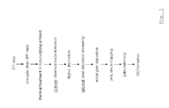
- Figure 1 represents the process flow for surface preparation according to the present invention.
- Figure 2 depicts the thickness measured by Angle Resolved X-Ray Photoelectron Spectroscopy (AR-XPS) for the interfacial layer and for the deposited high-k dielectric material HfO2 for different growth conditions.
- AR-XPS Angle Resolved X-Ray Photoelectron Spectroscopy
- Figure 3 represents the HfO2 coverage versus oxide thickness.
- Figure 4 represents the step-by-step oxide growth measured by Ellipsometry.
- FIG. 5 depicts a surface roughness check by Atomic Force Microscope (AFM).
- AFM Atomic Force Microscope
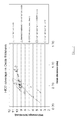
- Figure 6 is a capacitance versus voltage curve for different surface treatments.
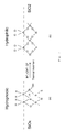
- Figure 7 shows schematically a possible mechanism for the thin interfacial layer formation.
- the present invention is based on the surprising observation that carrying out a method of the invention, comprising a thermal treatment in a non-oxidizing ambient comprising an inert gas, results in forming a thin interfacial layer (IL).
- a method of the invention comprising a thermal treatment in a non-oxidizing ambient comprising an inert gas, results in forming a thin interfacial layer (IL).
- non-oxidizing ambient means an oxygen-free ambient.
- Said ambient preferably comprises an inert gas ambient or mixture and optionally other additives.
- adding H2 to the non-oxidizing ambient comprising an inert gas ambient or mixture leads to increasing the surface smoothening of said thin interfacial layer.
- said thermal treatment is performed after cleaning the substrate and prior to the deposition of a high-k dielectric material.
- high-k dielectric denotes any dielectric material having a dielectric constant (relative to a vacuum), k, higher than 3.9 (which is the dielectric constant of SiO2) and more preferably having a dielectric constant higher than 8.0.
- Performing said thermal treatment in a non-oxidizing ambient comprising an inert gas results in the formation of a thin interfacial layer.
- Said interfacial layer may contain silicon oxides and sub-oxides (SiO x with 0 ⁇ x ⁇ 2).
- the originality of the present method is that a uniform (smooth or flat) thin (having a thickness below about 10 angstroms) interfacial layer is formed exhibiting reasonable leakage and enhancing mobility of the charge carriers whereas using prior art techniques a low quality interfacial layer (being rough (neither flat, nor smooth, nor uniform) and showing no continuous interfacial oxide growth) is generated, yielding higher leakage and higher interface trap density (D it ), and as a consequence, low performance semiconductor devices.
- This native oxide layer is essentially a heterogeneous mixture of SiO and SiO2.
- the substrate is cleaned of, among other things, native oxide, to avoid contamination and produce superior electrical properties.
- cleaning the substrate comprises a HF-last hydrophobic treatment, suppressing the oxygen radical to combine with silicon.
- Said HF-last hydrophobic treatment is based on an oxidation step using ozone and deionized water (O3/DIW) followed by an oxide removal step (using HF/HCl).
- O3/DIW deionized water
- oxide removal step using HF/HCl.
- DIW with HCl spiking a deionized-water rinse
- IPA/N2 Marangoni drying with isopropyl alcohol and nitrogen
- Said HF-last (IMEC-foob) treatment results in an oxide free surface.
- said oxide-free surface generated after said HF-last (IMEC-foob) clean does not provide the proper OH-bond termination suitable for further depositing a high-k material.
- Said thermal treatment leads to the formation of a uniform thin interfacial layer of oxides and/or suboxides, located between said gate dielectric and said semiconductor substrate.
- Said thin interfacial oxide/sub-oxides layer resulting from performing said thermal treatment in a non-oxidizing ambient, is defined as a thin interfacial layer in inert ambient.
- FIG. 1 a flowchart illustrates the sequence of the different steps in a semiconductor manufacturing process according to the method of the invention.
- the method can comprise forming isolation structures such as Shallow Trench Isolation (STI) structures in a semiconductor body.
- isolation structures such as Shallow Trench Isolation (STI) structures in a semiconductor body.
- Gate fabrication begins where a HF-last hydrophobic (IMEC-foob) treatment is performed to clean a top surface of the semiconductor body before performing the thermal treatment in a non-oxidizing ambient.
- a HF-last hydrophobic (IMEC-foob) treatment is performed to clean a top surface of the semiconductor body before performing the thermal treatment in a non-oxidizing ambient.
- Performing said thermal treatment step in a non-oxidizing ambient comprising an inert gas yields a high quality thin interfacial layer formed over the semiconductor body.
- a chemical oxide is optionally formed performing either said wet O3/DIW-last cleaning treatment (also called IMEC-clean) or said UV-enhanced oxide growth method, leaving the surface with a thin chemical oxide layer.
- the method proceeds where a high-k gate dielectric is deposited over the interface layer.
- the high-k gate dielectric can comprise one or more layers of high-k dielectric material.
- the high-k dielectric material deposition is optionally followed by a post deposition anneal.
- a conductive metal gate contact (or gate electrode) is then formed over the high-k gate dielectric, thereby forming the gate structure or gate stack.
- the gate electrode can comprise one or more layers of conductive material.
- a polysilicon capping layer is deposited over the gate contact.
- the gate contact, the (high-k) gate dielectric and the interface layer are then patterned to form a gate structure.
- Source/drain regions of the semiconductor body are provided with appropriate n or p dopants through implantation and diffusion and interconnect processing is performed.
- grooves formed by dry-etch in the substrate are filled with a dielectric material providing electrical insulation.
- the gate dielectric can be a high-k dielectric material such as a hafnium oxide, an aluminium oxide, or a zirconium oxide.
- the gate electrode (or gate contact) can be formed from a semiconductor material such as polysilicon, silicon-germanium, germanium, metal silicides or from a metallic material selected from the group consisting of metals, metal nitrides, metal carbonitrides, and combinations thereof (e.g. Ti, Ta, W, Ru, Ti(C)N, Ta(C)N, W(C)N).
- a semiconductor material such as polysilicon, silicon-germanium, germanium, metal silicides or from a metallic material selected from the group consisting of metals, metal nitrides, metal carbonitrides, and combinations thereof (e.g. Ti, Ta, W, Ru, Ti(C)N, Ta(C)N, W(C)N).
- a gate structure separates in a lateral direction the source electrode and the drain electrode, which contact at opposite lateral sides the channel region.
- dielectric sidewall spacers can be formed to offset the source and drain regions from the channel region.
- These sidewall spacers can be formed for example from silicon-oxide, silicon-nitride, and/or silicon-carbide.
- a method for forming a high-k gate dielectric comprises the steps of providing a semiconductor substrate, cleaning the substrate, performing a thermal treatment in a non-oxidizing ambient and then performing a high-k dielectric material deposition.
- performing said thermal treatment in a non-oxidizing ambient, further comprising an inert gas mixture leads to the formation of a thin interfacial layer.
- said uniform thin interfacial layer as a result of the applied thermal treatment, has the suitable surface terminations and thus makes the surface compatible with high-k material deposition and minimizes the EOT.
- Said uniform thin interfacial layer provides improved interface characteristics between the silicon structure and the high-k dielectric material deposited in the following deposition step.
- Said thermal treatment in a non-oxidizing ambient comprising an inert gas mixture is preferably performed in a Rapid Thermal Process (RTP) chamber.
- RTP Rapid Thermal Process
- Said thermal treatment is preferably performed at a temperature higher than 700°C, more preferably higher than 1000°C and preferably higher than 1050°C.
- the duration of said thermal treatment is preferably less than 2 minutes, more preferably less than 1 minute, preferably less than 40 seconds.
- the thermal treatment can also be performed in a furnace (e.g. LPCVD Low Pressure Chemical Vapor Deposition reactor) or using a spike anneal.
- a furnace e.g. LPCVD Low Pressure Chemical Vapor Deposition reactor
- a spike anneal When performed in a LPCVD reactor the thermal treatment requires longer duration (at least 10 minutes up to several hours), while the spike anneal takes typically 1s at approximately 1050°C.
- Said inert gas in said non-oxidizing ambient used during said thermal treatment is preferably He and/or Ar.
- N2 gas is not appropriate to be added to the non-oxidizing ambient as it would incorporate at the interface and increase interface state density leading to degradation of the channel mobility, affecting in this way the electrical characteristics of the device.
- a proportion of H2 is added to the non-oxidizing ambient comprising said inert gas.
- the proportion of the H2 gas is by volume less than 10%, and more preferably comprised between 1 and 10%.
- the pressure of the non-oxidizing ambient is comprised between 10 and 20 torr.
- the method according to the invention is used for obtaining a thickness of the thin interfacial layer being less than 0.6 nm.
- the method according to the invention is used for obtaining a good quality interfacial layer being flat (or smooth or uniform) and showing continuous interfacial oxide growth.
- the formation of said thin interfacial layer is followed by the deposition of a high-k dielectric material.
- Said high-k dielectric material can be deposited using any deposition techniques known in the art, and preferably using Atomic Layer Deposition (ALD), Metal-Organic Chemical Vapor Deposition (MOCVD), Molecular Beam Epitaxy (MBE), Chemical Vapor Deposition (CVD), or Physical Vapor Deposition (PVD).
- ALD Atomic Layer Deposition
- MOCVD Metal-Organic Chemical Vapor Deposition
- MBE Molecular Beam Epitaxy
- CVD Chemical Vapor Deposition
- PVD Physical Vapor Deposition
- high-k materials include, but are not limited to binary metal oxides including ZrO2, HfO2, La2O3, Y2O3, TiO2, as well as their silicates and aluminates; metal oxynitrides including AlON, ZrON, HfON, LaON, YON, as well as their silicates and aluminates such as ZrSiON, HfSiON, LaSiON, YsiON etc.; and perovskite type oxides including a titanate system material such as barium titanate, strontium titanate, barium strontium titanate (BaSr) Ti03 (BST).
- binary metal oxides including ZrO2, HfO2, La2O3, Y2O3, TiO2, as well as their silicates and aluminates
- metal oxynitrides including AlON, ZrON, HfON, LaON, YON, as well as their silicates and aluminates such as ZrSiON, HfSiON
- the high-k material deposition step is optionally followed by a post deposition anneal step further lowering the Interface Trap Density (D it ).
- the high-k material deposition step is immediately performed after performing said thermal treatment in a non-oxidizing ambient.
- a chemical oxide growth step is optionally performed after performing said thermal treatment in a non-oxidizing ambient.
- Chemically growing oxide involves contacting a bare semiconductor surface and more preferably said thin interfacial layer with liquid and/or gaseous chemical(s) that oxidize the surface.
- said chemical oxide is preferably formed performing either a wet cleaning treatment such as an O3/DIW-last (IMEC-clean) treatment or a UV-enhanced oxide growth, both used now as an alternative to grow a thin chemical oxide layer.
- a wet cleaning treatment such as an O3/DIW-last (IMEC-clean) treatment
- a UV-enhanced oxide growth both used now as an alternative to grow a thin chemical oxide layer.
- Said wet O3/DIW-last clean is based on an oxidation step using ozone and deionized water (O3/DIW) followed by an oxide removal step (using HF/HCl).
- O3/DIW ozone and deionized water
- oxide removal step using HF/HCl
- an ozonated deionized-water rinse O3/DIW with HCl spiking
- Marangoni drying with isopropyl alcohol and nitrogen IPA/N2
- Said UV-enhanced oxide growth method consists in growing a thin oxide layer in air under UV radiation. Argon is flushed continuously over the substrate to slow down the growth rate of the oxide in air.
- Said UV-enhanced oxide growth method results in a chemical oxide layer which is thinner than the one formed during the wet 03/DIW-last clean (IMEC-clean) treatment.
- Said chemical oxide layer grown by performing said wet O3/DIW-last clean (IMEC-clean) or said UV-enhanced oxide growth method also provide, in addition to the effect caused by performing the thermal treatment, a surface with suitable terminations (e.g. OH-bonds) enabling the following high-k material deposition.
- IMEC-clean wet O3/DIW-last clean
- UV-enhanced oxide growth method also provide, in addition to the effect caused by performing the thermal treatment, a surface with suitable terminations (e.g. OH-bonds) enabling the following high-k material deposition.
- a total oxide layer can be formed which can be divided into two contributions; on the one hand an interfacial layer yielded by performing said thermal treatment in said non-oxidizing ambient and on the other hand said chemical oxide layer grown by performing either said wet O3/DIW-last clean (IMEC-clean) treatment or said UV-enhanced oxide growth method.
- an interfacial layer yielded by performing said thermal treatment in said non-oxidizing ambient
- said chemical oxide layer grown by performing either said wet O3/DIW-last clean (IMEC-clean) treatment or said UV-enhanced oxide growth method.
- the ALD high-k material deposition step is performed.
- Said semiconductor substrate is preferably a silicon substrate or a Silicon-On-Insulator (SOI) substrate comprising a silicon wafer or silicon layer, such as polysilicon, epitaxial silicon or amorphous silicon, with or without dopants for electrical conductivity.
- SOI Silicon-On-Insulator
- Said semiconductor substrate can be any semiconductor substrate that is resistant at the required high temperatures used according to the present invention.
- the substrate may contain various isolation regions such as Shallow Trench Isolation (STI) regions, LOCOS (local oxidation of silicon) regions or other like isolation regions either formed in the substrate or on a surface thereof.
- STI Shallow Trench Isolation
- LOCOS local oxidation of silicon
- Figure 2 shows the thickness measured by AR-XPS for the interfacial layer and for the deposited high-k dielectric material HfO2 for different surface treatment steps according to the method of the invention.
- the interfacial layer (IL) in Figure 2 is formed either as a result of said thermal treatment in non-oxidizing ambient, or it is a grown chemical oxide layer with/without previous thermal treatment.
- Said chemical oxide is formed either by performing said wet O3/DIW-last cleaning treatment (also called IMEC-clean) or said UV-enhanced oxide growth method (labeled UV/Air/Ar in Figure 2 ).
- Figure 2 shows very good results for the thickness for both the interfacial layer and the deposited high-k dielectric HfO2 layer performing only said thermal treatment.
- the H2/He/1050°C thermal treatment and the He/1050°C thermal treatment form an ultrathin interfacial layer of 0.4 nm and 0.5 nm respectively.
- the H2/He/1050°C thermal treatment helps to limit the following chemical oxide growth.
- the method according to the invention can be used for achieving EOT scaling.
- the thickness of the total oxide layer is also lower than in the case performing only a chemical oxide growth via said UV-enhanced oxide growth method.
- performing said UV-enhanced oxide growth method yields a lower HfO2 coverage than performing said thermal treatment in combination with said UV-enhanced oxide growth.
- a possible explanation is that the UV-enhanced oxide does not show enough appropriate active group terminations (e.g. OH-bonds) on the surface, which makes it a rough and low quality nucleation layer for the following high-k material deposition step and, as such, yielding problems in electrical properties of the resulting devices.
- Figure 3 represents the Hf02 coverage (atoms/cm2) versus oxide thickness according to the present invention.
- the interfacial layer is formed by performing said thermal treatment optionally followed by said chemical oxide formation (performed by said UV-enhanced oxide growth method or by said wet O3/DIW-last treatment (IMEC-clean)).
- Said interfacial layer formation is then followed by e.g. a five cycle ALD Hf02 monolayer deposition.
- the ALD technique in general and ALD of HfO2 in particular is sensitive to the interfacial layer surface conditions and, as such, by performing ALD of HfO2 the interface layer quality is evaluated according to its roughness, the termination of the active groups on its surface (e.g. OH-bonds) and the continuity/uniformity of the interfacial layer (e.g. not-island-like).
- performing said thermal treatment forming said interfacial layer provides the best HfO2 coverage and thus a good quality, smooth interfacial layer.
- Said HfO2 coverage is also higher than the one obtained by performing O3/DIW chemical oxide growth (combined with or without thermal treatment forming interfacial layer) and especially improving the poor coverage obtained by performing said UV-enhanced oxide growth method only.
- Figure 4 represents the step-by-step oxide thickness (measured by Ellipsometry) for different surface treatment steps according to the method of the invention.
- IMFOOB IMFOOB
- thermal treatment in a non-oxidizing ambient
- chemical oxide growth wet O3/DIW-last clean (IMEC clean) or UV/Air/Ar
- the chemical oxide is grown by performing said UV-enhanced oxide growth method or by a wet O3/DIW-last treatment (IMEC clean).
- the total oxide layer depicted in Figure 4 is measured upon forming said interfacial layer yielded by performing said thermal treatment in said non-oxidizing ambient and said chemical oxide layer grown by performing either said wet O3/DIW-last clean (IMEC-clean) treatment or said UV-enhanced oxide growth method.
- IMEC-clean wet O3/DIW-last clean
- optical Ellipsometry is not as precise as AR-XPS for measuring the oxide thickness for thin layers.
- the thickness measured by Ellipsometry is thicker than the corresponding one measured via AR-XPS.
- FIG. 5 depicts a surface roughness measurement by Atomic Force Microscope (AFM).
- AFM Atomic Force Microscope
- Either a thermal treatment is performed yielding an interfacial layer and/or a chemical oxide is grown.
- the chemical oxide is grown by performing said UV-enhanced oxide growth method or by a wet 03/DIW treatment (Imec clean).
- a chemical oxide layer grown using only said UV-enhanced oxide growth method or only an O3/DIW treatment thus treatments without performing a thermal (pre)treatment forming an interfacial layer, yield relative rough surfaces of the oxide layer.
- a capacitance versus voltage curve for the case of thermal treatment only, chemical oxide growth only, or the combination thermal treatment and chemical oxide growth is given in Figure 6 .
- the capacitor (MOS) is a p-type substrate having a TaN/TiN metal gate electrode.
- the leakage is suppressed by forming first an interfacial layer with or without performing said UV-enhanced oxide growth method.
- FIG 7 shows schematically a possible mechanism for the thin interfacial layer formation.
- the cleaning sequence comprises a HF-last hydrophobic treatment that leave a hydrogen terminated surface (Si-H bonds, Figure 7a ), that are suppressing the oxygen radical to combine with the silicon top layer.
- Si-H bonds Si-H bonds
- dissolved O2 and/or OH - radicals may attack the interior Si-Si bonds without breaking the Si-H bonds, leaving SiO x sub-oxides under the (oxide-free) surface.
- a thin layer comprising silicon oxides and sub-oxides (SiO x with 0 ⁇ x ⁇ 2) is unraveled on the silicon surface ( Figure 7b ).
- the thin layer is continuous (no islands formations), uniform and hydrophilic, being a suitable interface layer between the substrate and the high-k materials (e.g. Hf-oxides) deposited with ALD.
- a method for producing a uniform ultrathin interfacial layer underneath materials of high dielectric permittivity i.e. high-k materials.
- the method according to the invention can be used for yielding a uniform and thin interfacial layer with suitable terminations (e.g. OH-bonds) making it compatible with the following high-k material deposition step.
- suitable terminations e.g. OH-bonds
- the mobility of the charge carriers in the semiconductor device is enhanced.
Landscapes
- Insulated Gate Type Field-Effect Transistor (AREA)
- Formation Of Insulating Films (AREA)
- Chemical & Material Sciences (AREA)
- Chemical Kinetics & Catalysis (AREA)
- Crystallography & Structural Chemistry (AREA)
- General Chemical & Material Sciences (AREA)
- Thin Film Transistor (AREA)
Abstract
- providing a semiconductor substrate,
- cleaning the substrate,
- performing a thermal treatment ,
- performing a high-k dielectric material deposition,
characterised in that said thermal treatment step is performed in a non-oxidizing ambient, leading to the formation of a thin interfacial layer.
Description
- The present invention is related to the field of integrated circuit (IC) fabrication.
- More precisely, the present invention is related to a method for depositing a high-k dielectric material on a substrate thereby providing a suitable interface layer for high-k material deposition.
- In particular, the present invention concerns methods for depositing high-k dielectric materials when making gate dielectric structures.
- At present, there is a great demand for shrinking (or scaling) semiconductor devices to provide an increased density of devices on the semiconductor chip that are faster and consume less power.
- Si02 has been the most used gate dielectric material of semiconductor devices. However, scaling the thickness of Si02 for gate dielectric applications has placed severe limitations on the oxidation process. Sub-angstrom uniformity across the wafer and thickness control are needed requirements to use these dielectric materials.
- Furthermore, as the thickness of the dielectric layer is reduced, quantum tunneling effects tend to increase, allowing an electric current to flow between the gate and the channel. This tunneling current is undesirable.
- Recent efforts involving device scaling have focused on alternative dielectric materials which can be formed in a thicker layer than for example scaled SiO2 layers and yet still produce the same field effect performance. These materials are often referred to as high-k materials because their dielectric constants are higher than that of SiO2 (dielectric constant k of SiO2 being 3.9).
- The relative performance of such high-k materials is often expressed as Equivalent Oxide Thickness (EOT), because the alternative material layer may be thicker, while still providing the equivalent electrical effect of a much thinner layer of SiO2.
- But, a drawback of using higher k dielectric materials is that they tend to provide poor quality interfaces. This poor quality of the interface tends to impair the electrical performance of the resultant gate electrode microstructure in those instances in which a higher k dielectric material is deposited directly onto the silicon substrate.
- Therefore, as described in prior patent art
WO 2005/013349 , dielectric materials, such as SiO2 or the like, can provide a buffer (or interface or bridge) between a semiconductor wafer and a high-k dielectric material to improve electrical performance when using high-k dielectric materials. - Unfortunately, it has been very difficult to develop extremely thin interfacial layers (e.g. those having a thickness below about 10 angstroms) with desired uniformity characteristics.
- This lack of uniformity can impair electrical properties of the resultant devices.
- In order to integrate high-k materials into current CMOS processing schemes, an interfacial layer of good quality (being flat, smooth, and uniform) and showing continuous interfacial oxide growth) would be beneficial between the semiconductor substrate and the deposited high-k material.
- One challenge here is to optimize this quality of the interface between a semiconductor wafer substrate (especially silicon wafer substrates) and the higher k dielectric material, upon which the performance and the reliability of the resultant transistors depend.
- The present invention aims to provide an improved and alternative method which does not present the drawbacks of prior art techniques.
- The present invention aims to provide a method which is particularly advantageous for producing a uniform ultrathin interfacial layer suitable for deposition of dielectric materials with high permittivity (i.e. high-k materials).
- Furthermore, the present invention aims to improve the interface between a semiconductor substrate (or wafer) and a dielectric layer, in particular a high-k dielectric material deposited thereon.
- The present invention provides a method for forming a high-k gate dielectric, comprising the steps of:
- providing a semiconductor substrate,
- cleaning the substrate,
- performing a thermal treatment,
- performing a high-k dielectric material deposition for forming the gate dielectric,
- Preferably, said step of cleaning the substrate comprises a HF-last treatment (also referred to as IMEC-foob treatment).
- Preferably, in a method of the invention, said thermal treatment step is performed at a temperature higher than 700°C, preferably higher than 1000°C and more preferably higher than 1050°C.
- Preferably, in a method of the invention, said non-oxidizing ambient comprises an inert gas, preferably He and/or Ar.
- Preferably, in a method of the invention, a proportion of H2 is added to the non-oxidizing ambient.
- Preferably, said proportion of said H2 gas is by volume less than or equal to 10%, and preferably comprised between 1 and 10%.
- Preferably, N2 is excluded from said non-oxidizing ambient.
- Preferably, in a method of the invention, the duration of said thermal treatment step is less than 2 minutes, preferably less than 1 minute, more preferably less than 40 seconds.
- Preferably, in the method according to the invention, said thermal treatment step is followed by a step of forming a thin chemical oxide layer.
- Preferably, said thin chemical oxide layer is formed by performing a wet 03/DIW-last treatment (also referred to as IMEC-clean treatment) or a UV-enhanced oxide growth method.
- Preferably, in the method according to the invention, said high-k dielectric material is any dielectric material with a dielectric constant, k, higher than the dielectric constant of SiO2.
- Preferably, said high-k dielectric material is deposited by Atomic Layer Deposition (ALD).
- Preferably, in the method of the invention, the step of depositing the high-k dielectric material is followed by a post deposition anneal step.
- Preferably, the thickness of said thin interfacial layer is less than 0.6 nm.
- The method according to the present invention can be used for fabricating a semiconductor device incorporating a high-k gate dielectric.
- Preferably, said semiconductor device incorporates a high-k gate dielectric comprising a thin interfacial layer of less than 0.6 nm.
-
Figure 1 represents the process flow for surface preparation according to the present invention. -
Figure 2 depicts the thickness measured by Angle Resolved X-Ray Photoelectron Spectroscopy (AR-XPS) for the interfacial layer and for the deposited high-k dielectric material HfO2 for different growth conditions. -
Figure 3 represents the HfO2 coverage versus oxide thickness. -
Figure 4 represents the step-by-step oxide growth measured by Ellipsometry. -
Figure 5 depicts a surface roughness check by Atomic Force Microscope (AFM). -
Figure 6 is a capacitance versus voltage curve for different surface treatments. -
Figure 7 shows schematically a possible mechanism for the thin interfacial layer formation. - The present invention is based on the surprising observation that carrying out a method of the invention, comprising a thermal treatment in a non-oxidizing ambient comprising an inert gas, results in forming a thin interfacial layer (IL).
- The term "non-oxidizing ambient" as used in the present invention means an oxygen-free ambient. Said ambient preferably comprises an inert gas ambient or mixture and optionally other additives.
- More particularly, adding H2 to the non-oxidizing ambient comprising an inert gas ambient or mixture leads to increasing the surface smoothening of said thin interfacial layer.
- In the present method, said thermal treatment is performed after cleaning the substrate and prior to the deposition of a high-k dielectric material.
- The term "high-k dielectric" as used in the present invention denotes any dielectric material having a dielectric constant (relative to a vacuum), k, higher than 3.9 (which is the dielectric constant of SiO2) and more preferably having a dielectric constant higher than 8.0.
- Performing said thermal treatment in a non-oxidizing ambient comprising an inert gas results in the formation of a thin interfacial layer.
- Said interfacial layer may contain silicon oxides and sub-oxides (SiOx with 0 < x ≤ 2).
- The originality of the present method is that a uniform (smooth or flat) thin (having a thickness below about 10 angstroms) interfacial layer is formed exhibiting reasonable leakage and enhancing mobility of the charge carriers whereas using prior art techniques a low quality interfacial layer (being rough (neither flat, nor smooth, nor uniform) and showing no continuous interfacial oxide growth) is generated, yielding higher leakage and higher interface trap density (Dit), and as a consequence, low performance semiconductor devices.
- It is known that native oxide is growing on the bare Si substrate when exposed to ambient atmosphere comprising oxygen.
- This native oxide layer is essentially a heterogeneous mixture of SiO and SiO2.
- The quality and thickness of this native oxide layer is inconsistent across the substrate surface and, as such, these native oxide films on Si surfaces prevent the precise control of the thickness of ultrathin gate oxide films.
- Therefore, the substrate is cleaned of, among other things, native oxide, to avoid contamination and produce superior electrical properties.
- Usually, cleaning the substrate comprises a HF-last hydrophobic treatment, suppressing the oxygen radical to combine with silicon.
- Said HF-last hydrophobic treatment, also called IMEC-foob, is based on an oxidation step using ozone and deionized water (O3/DIW) followed by an oxide removal step (using HF/HCl). At the end, a deionized-water rinse (DIW with HCl spiking) followed by Marangoni drying with isopropyl alcohol and nitrogen (IPA/N2) is applied.
- Said HF-last (IMEC-foob) treatment results in an oxide free surface.
- But, said oxide-free surface generated after said HF-last (IMEC-foob) clean does not provide the proper OH-bond termination suitable for further depositing a high-k material.
- In the present invention, it was suggested to perform, after said cleaning step of the substrate, a thermal treatment in a non-oxidizing ambient.
- Said thermal treatment leads to the formation of a uniform thin interfacial layer of oxides and/or suboxides, located between said gate dielectric and said semiconductor substrate.
- Said thin interfacial oxide/sub-oxides layer, resulting from performing said thermal treatment in a non-oxidizing ambient, is defined as a thin interfacial layer in inert ambient.
- In
Figure 1 , a flowchart illustrates the sequence of the different steps in a semiconductor manufacturing process according to the method of the invention. - The method can comprise forming isolation structures such as Shallow Trench Isolation (STI) structures in a semiconductor body.
- Gate fabrication begins where a HF-last hydrophobic (IMEC-foob) treatment is performed to clean a top surface of the semiconductor body before performing the thermal treatment in a non-oxidizing ambient.
- Performing said thermal treatment step in a non-oxidizing ambient comprising an inert gas yields a high quality thin interfacial layer formed over the semiconductor body.
- Then, a chemical oxide is optionally formed performing either said wet O3/DIW-last cleaning treatment (also called IMEC-clean) or said UV-enhanced oxide growth method, leaving the surface with a thin chemical oxide layer.
- After the interface layer has been formed the method proceeds where a high-k gate dielectric is deposited over the interface layer. The high-k gate dielectric can comprise one or more layers of high-k dielectric material.
- The high-k dielectric material deposition is optionally followed by a post deposition anneal.
- A conductive metal gate contact (or gate electrode) is then formed over the high-k gate dielectric, thereby forming the gate structure or gate stack.
- The gate electrode can comprise one or more layers of conductive material.
- Furthermore, a polysilicon capping layer is deposited over the gate contact.
- The gate contact, the (high-k) gate dielectric and the interface layer are then patterned to form a gate structure.
- Source/drain regions of the semiconductor body are provided with appropriate n or p dopants through implantation and diffusion and interconnect processing is performed.
- In the case of shallow-trench-isolation, grooves formed by dry-etch in the substrate are filled with a dielectric material providing electrical insulation.
- The gate dielectric can be a high-k dielectric material such as a hafnium oxide, an aluminium oxide, or a zirconium oxide.
- The gate electrode (or gate contact) can be formed from a semiconductor material such as polysilicon, silicon-germanium, germanium, metal silicides or from a metallic material selected from the group consisting of metals, metal nitrides, metal carbonitrides, and combinations thereof (e.g. Ti, Ta, W, Ru, Ti(C)N, Ta(C)N, W(C)N).
- A gate structure separates in a lateral direction the source electrode and the drain electrode, which contact at opposite lateral sides the channel region.
- Against the gate structure, dielectric sidewall spacers can be formed to offset the source and drain regions from the channel region. These sidewall spacers can be formed for example from silicon-oxide, silicon-nitride, and/or silicon-carbide.
- According to a preferred embodiment, a method for forming a high-k gate dielectric comprises the steps of providing a semiconductor substrate, cleaning the substrate, performing a thermal treatment in a non-oxidizing ambient and then performing a high-k dielectric material deposition.
- According to the present method, performing said thermal treatment in a non-oxidizing ambient, further comprising an inert gas mixture, leads to the formation of a thin interfacial layer.
- Furthermore, said uniform thin interfacial layer, as a result of the applied thermal treatment, has the suitable surface terminations and thus makes the surface compatible with high-k material deposition and minimizes the EOT.
- Said uniform thin interfacial layer provides improved interface characteristics between the silicon structure and the high-k dielectric material deposited in the following deposition step.
- Said thermal treatment in a non-oxidizing ambient comprising an inert gas mixture is preferably performed in a Rapid Thermal Process (RTP) chamber.
- Said thermal treatment is preferably performed at a temperature higher than 700°C, more preferably higher than 1000°C and preferably higher than 1050°C.
- The duration of said thermal treatment is preferably less than 2 minutes, more preferably less than 1 minute, preferably less than 40 seconds.
- In a method according to the invention, the thermal treatment can also be performed in a furnace (e.g. LPCVD Low Pressure Chemical Vapor Deposition reactor) or using a spike anneal. When performed in a LPCVD reactor the thermal treatment requires longer duration (at least 10 minutes up to several hours), while the spike anneal takes typically 1s at approximately 1050°C.
- During the thermal treatment, a uniform thin layer comprising silicon oxides and sub-oxides (SiOx with 0 < x ≤ 2) is unraveled on the substrate surface.
- Said inert gas in said non-oxidizing ambient used during said thermal treatment is preferably He and/or Ar.
- N2 gas is not appropriate to be added to the non-oxidizing ambient as it would incorporate at the interface and increase interface state density leading to degradation of the channel mobility, affecting in this way the electrical characteristics of the device.
- Preferably, a proportion of H2 is added to the non-oxidizing ambient comprising said inert gas.
- Preferably the proportion of the H2 gas is by volume less than 10%, and more preferably comprised between 1 and 10%.
- Preferably, the pressure of the non-oxidizing ambient is comprised between 10 and 20 torr.
- As such, the method according to the invention is used for obtaining a thickness of the thin interfacial layer being less than 0.6 nm.
- Furthermore, the method according to the invention is used for obtaining a good quality interfacial layer being flat (or smooth or uniform) and showing continuous interfacial oxide growth.
- In the present method, the formation of said thin interfacial layer is followed by the deposition of a high-k dielectric material.
- Said high-k dielectric material can be deposited using any deposition techniques known in the art, and preferably using Atomic Layer Deposition (ALD), Metal-Organic Chemical Vapor Deposition (MOCVD), Molecular Beam Epitaxy (MBE), Chemical Vapor Deposition (CVD), or Physical Vapor Deposition (PVD).
- Examples of high-k materials include, but are not limited to binary metal oxides including ZrO2, HfO2, La2O3, Y2O3, TiO2, as well as their silicates and aluminates; metal oxynitrides including AlON, ZrON, HfON, LaON, YON, as well as their silicates and aluminates such as ZrSiON, HfSiON, LaSiON, YsiON etc.; and perovskite type oxides including a titanate system material such as barium titanate, strontium titanate, barium strontium titanate (BaSr) Ti03 (BST).
- Preferably, the high-k material deposition step is optionally followed by a post deposition anneal step further lowering the Interface Trap Density (Dit).
- In one embodiment, the high-k material deposition step is immediately performed after performing said thermal treatment in a non-oxidizing ambient.
- In another embodiment, a chemical oxide growth step is optionally performed after performing said thermal treatment in a non-oxidizing ambient.
- Chemically growing oxide involves contacting a bare semiconductor surface and more preferably said thin interfacial layer with liquid and/or gaseous chemical(s) that oxidize the surface.
- According to the present invention, said chemical oxide is preferably formed performing either a wet cleaning treatment such as an O3/DIW-last (IMEC-clean) treatment or a UV-enhanced oxide growth, both used now as an alternative to grow a thin chemical oxide layer.
- Said wet O3/DIW-last clean, also known as IMEC-clean, is based on an oxidation step using ozone and deionized water (O3/DIW) followed by an oxide removal step (using HF/HCl). At the end, an ozonated deionized-water rinse (O3/DIW with HCl spiking) followed by Marangoni drying with isopropyl alcohol and nitrogen (IPA/N2) is applied.
- Said wet O3/DIW-last clean (IMEC-clean) is leaving the surface with a very clean thin chemical oxide layer.
- Said UV-enhanced oxide growth method consists in growing a thin oxide layer in air under UV radiation. Argon is flushed continuously over the substrate to slow down the growth rate of the oxide in air.
- Said UV-enhanced oxide growth method results in a chemical oxide layer which is thinner than the one formed during the wet 03/DIW-last clean (IMEC-clean) treatment.
- Said chemical oxide layer grown by performing said wet O3/DIW-last clean (IMEC-clean) or said UV-enhanced oxide growth method also provide, in addition to the effect caused by performing the thermal treatment, a surface with suitable terminations (e.g. OH-bonds) enabling the following high-k material deposition.
- As such, a total oxide layer can be formed which can be divided into two contributions; on the one hand an interfacial layer yielded by performing said thermal treatment in said non-oxidizing ambient and on the other hand said chemical oxide layer grown by performing either said wet O3/DIW-last clean (IMEC-clean) treatment or said UV-enhanced oxide growth method.
- Performing only said chemical oxide growth step without performing a thermal (pre)treatment, yields a leaky, poor quality chemical oxide (cf.
Figure 3 andFigure 6 discussed below) not suitable for further high-k material deposition and, as a consequence, yielding low quality semiconductor devices. - Then, after said optional chemical oxide formation step, the ALD high-k material deposition step is performed.
- Said semiconductor substrate is preferably a silicon substrate or a Silicon-On-Insulator (SOI) substrate comprising a silicon wafer or silicon layer, such as polysilicon, epitaxial silicon or amorphous silicon, with or without dopants for electrical conductivity.
- Said semiconductor substrate can be any semiconductor substrate that is resistant at the required high temperatures used according to the present invention.
- The substrate may contain various isolation regions such as Shallow Trench Isolation (STI) regions, LOCOS (local oxidation of silicon) regions or other like isolation regions either formed in the substrate or on a surface thereof.
-
Figure 2 shows the thickness measured by AR-XPS for the interfacial layer and for the deposited high-k dielectric material HfO2 for different surface treatment steps according to the method of the invention. - The interfacial layer (IL) in
Figure 2 is formed either as a result of said thermal treatment in non-oxidizing ambient, or it is a grown chemical oxide layer with/without previous thermal treatment. - For the thermal treatment, different conditions concerning the composition of the non-oxidizing ambient and the temperature are indicated in
Figure 2 . - Said chemical oxide is formed either by performing said wet O3/DIW-last cleaning treatment (also called IMEC-clean) or said UV-enhanced oxide growth method (labeled UV/Air/Ar in
Figure 2 ). -
Figure 2 shows very good results for the thickness for both the interfacial layer and the deposited high-k dielectric HfO2 layer performing only said thermal treatment. - For example the H2/He/1050°C thermal treatment and the He/1050°C thermal treatment form an ultrathin interfacial layer of 0.4 nm and 0.5 nm respectively.
- Furthermore, as depicted in
Figure 2 , the H2/He/1050°C thermal treatment helps to limit the following chemical oxide growth. - Thus, the method according to the invention can be used for achieving EOT scaling.
- In the case of forming an interfacial layer as a result of performing said thermal treatment combined with a chemical oxide growth by said UV-enhanced oxide growth method, the thickness of the total oxide layer is also lower than in the case performing only a chemical oxide growth via said UV-enhanced oxide growth method.
- But, as shown in
Figure 3 , performing said UV-enhanced oxide growth method yields a lower HfO2 coverage than performing said thermal treatment in combination with said UV-enhanced oxide growth. A possible explanation is that the UV-enhanced oxide does not show enough appropriate active group terminations (e.g. OH-bonds) on the surface, which makes it a rough and low quality nucleation layer for the following high-k material deposition step and, as such, yielding problems in electrical properties of the resulting devices. - Indeed,
Figure 3 represents the Hf02 coverage (atoms/cm2) versus oxide thickness according to the present invention. - The interfacial layer is formed by performing said thermal treatment optionally followed by said chemical oxide formation (performed by said UV-enhanced oxide growth method or by said wet O3/DIW-last treatment (IMEC-clean)).
- Said interfacial layer formation is then followed by e.g. a five cycle ALD Hf02 monolayer deposition.
- The ALD technique in general and ALD of HfO2 in particular is sensitive to the interfacial layer surface conditions and, as such, by performing ALD of HfO2 the interface layer quality is evaluated according to its roughness, the termination of the active groups on its surface (e.g. OH-bonds) and the continuity/uniformity of the interfacial layer (e.g. not-island-like).
- Accordingly, more OH-group termination on the surface and smoother (lower roughness) interfacial layer is preferred by ALD of HfO2.
- As shown in
Figure 3 , performing said thermal treatment forming said interfacial layer (combined with or without performing said UV-enhanced oxide growth method) provides the best HfO2 coverage and thus a good quality, smooth interfacial layer. - Said HfO2 coverage is also higher than the one obtained by performing O3/DIW chemical oxide growth (combined with or without thermal treatment forming interfacial layer) and especially improving the poor coverage obtained by performing said UV-enhanced oxide growth method only.
-
Figure 4 represents the step-by-step oxide thickness (measured by Ellipsometry) for different surface treatment steps according to the method of the invention. - Each time a cleaning step is performed (IMFOOB) followed either by a thermal treatment in a non-oxidizing ambient, or by a chemical oxide growth (wet O3/DIW-last clean (IMEC clean) or UV/Air/Ar), or by the combination of both.
- For the formation of the interfacial layer as a result of the thermal treatment, different conditions are indicated concerning the composition of the non-oxidizing ambient and the temperature.
- The chemical oxide is grown by performing said UV-enhanced oxide growth method or by a wet O3/DIW-last treatment (IMEC clean).
- The total oxide layer depicted in
Figure 4 is measured upon forming said interfacial layer yielded by performing said thermal treatment in said non-oxidizing ambient and said chemical oxide layer grown by performing either said wet O3/DIW-last clean (IMEC-clean) treatment or said UV-enhanced oxide growth method. - Here, it has to be noticed that optical Ellipsometry is not as precise as AR-XPS for measuring the oxide thickness for thin layers.
- In fact, the thickness measured by Ellipsometry is thicker than the corresponding one measured via AR-XPS.
- But, the trend as shown in
Figure 4 is in agreement with the results shown inFigure 2 . -
Figure 5 depicts a surface roughness measurement by Atomic Force Microscope (AFM). - Either a thermal treatment is performed yielding an interfacial layer and/or a chemical oxide is grown.
- For the formation of the interfacial layer as a result of the thermal treatment, different conditions are indicated concerning the composition of the non-oxidizing ambient and the temperature.
- The chemical oxide is grown by performing said UV-enhanced oxide growth method or by a wet 03/DIW treatment (Imec clean).
- As shown in
Figure 5 , a chemical oxide layer grown using only said UV-enhanced oxide growth method or only an O3/DIW treatment, thus treatments without performing a thermal (pre)treatment forming an interfacial layer, yield relative rough surfaces of the oxide layer. For example, the chemical oxide formed by a wet O3/DIW-last clean (Imec clean) has an Rms = 0.18nm, while the UV-enhanced chemical oxide has an Rms = 0.14nm, Rms being measured each time for a 1 x 1µm scale. - On the contrary, performing a H2/He/1050°C thermal treatment forming an interfacial layer helps to smooth the surface of said thin interfacial layer and of the chemical oxide layer formed upon it, achieving Rms values of 0.08 to 0.09nm for a 1 x 1µm scale.
- Furthermore, a lower temperature treatment (e.g. 700°C) will degrade the surface smoothing performance (Rms = 0.146nm for a 1 x 1µm scale).
- A capacitance versus voltage curve for the case of thermal treatment only, chemical oxide growth only, or the combination thermal treatment and chemical oxide growth (UV-enhanced oxide labelled as UV/Air/Ar/1s) is given in
Figure 6 . - The capacitor (MOS) is a p-type substrate having a TaN/TiN metal gate electrode.
- Either a H2/He/1050°C thermal treatment is performed and/or said UV-enhanced oxide growth method is performed, followed by a 40 cycle ALD HfO2 monolayer deposition.
- From
Figure 6 it is shown that only performing said UV-enhanced oxide growth method yields a very leaky, thin oxide layer. - The leakage is suppressed by forming first an interfacial layer with or without performing said UV-enhanced oxide growth method.
-
Figure 7 shows schematically a possible mechanism for the thin interfacial layer formation. The cleaning sequence comprises a HF-last hydrophobic treatment that leave a hydrogen terminated surface (Si-H bonds,Figure 7a ), that are suppressing the oxygen radical to combine with the silicon top layer. In the presence of water (during the rinse step), dissolved O2 and/or OH- radicals may attack the interior Si-Si bonds without breaking the Si-H bonds, leaving SiOx sub-oxides under the (oxide-free) surface. During the thermal treatment, a thin layer comprising silicon oxides and sub-oxides (SiOx with 0 < x ≤ 2) is unraveled on the silicon surface (Figure 7b ). The thin layer is continuous (no islands formations), uniform and hydrophilic, being a suitable interface layer between the substrate and the high-k materials (e.g. Hf-oxides) deposited with ALD. - Thus, according to the invention, a method for producing a uniform ultrathin interfacial layer underneath materials of high dielectric permittivity (i.e. high-k materials) is provided.
- As such, the method according to the invention can be used for yielding a uniform and thin interfacial layer with suitable terminations (e.g. OH-bonds) making it compatible with the following high-k material deposition step.
- Furthermore, carrying out a method of the present invention improves interfacial layer roughness and quality.
- At the same time, in the framework of the present invention, the mobility of the charge carriers in the semiconductor device is enhanced.
Claims (16)
- A method for forming a high-k gate dielectric, comprising the steps of:- providing a semiconductor substrate,- cleaning the substrate,- performing a thermal treatment,- performing a high-k dielectric material deposition,characterised in that
said thermal treatment is performed in a non-oxidizing ambient, leading to the formation of a thin interfacial layer. - The method according to claim 1, wherein cleaning the substrate comprises a HF-last treatment.
- The method according to claims 1 and 2, wherein said thermal treatment is performed at a temperature higher than 700°C, preferably higher than 1000°C and preferably higher than 1050°C.
- The method according to any of the previous claims, wherein said non-oxidizing ambient comprises an inert gas, preferably He and/or Ar.
- The method according to any of the preceding claims, wherein a proportion of H2 is added to the non-oxidizing ambient.
- The method according to claim 5, wherein said proportion of the H2 gas is by volume less than 10%, and preferably comprised between 1 and 10%.
- The method according to any of the previous claims, wherein N2 is excluded from said non-oxidizing ambient.
- The method according to any of the previous claims, wherein the duration of the thermal treatment is less than 2 minutes, preferably less than 1 minute, preferably less than 40 seconds.
- The method according to any of the preceding claims, wherein said thermal treatment is followed by forming a thin chemical oxide layer.
- The method according to claim 9, wherein said thin chemical oxide layer is formed by performing a wet O3/DIW-last treatment or a UV-enhanced oxide growth method.
- The method according to any of the preceding claims, wherein the high-k dielectric material is any dielectric material with a dielectric constant, k, higher than the dielectric constant of SiO2.
- The method according to any of the preceding claims, wherein the high-k dielectric material is deposited by Atomic Layer Deposition.
- The method according to any of the preceding claims, wherein the high-k dielectric material deposition is followed by a post deposition anneal.
- The method according to any of the preceding claims, wherein the thickness of the thin interfacial layer is less than 0.6 nm.
- A semiconductor device incorporating a high-k gate dielectric obtainable by a method according to any of claims 1 to 14.
- A semiconductor device incorporating a high-k gate dielectric comprising a thin interfacial layer of less than 0.6 nm.
Priority Applications (6)
| Application Number | Priority Date | Filing Date | Title |
|---|---|---|---|
| EP07119632A EP2058844A1 (en) | 2007-10-30 | 2007-10-30 | Method of forming a semiconductor device |
| JP2008274400A JP5203133B2 (en) | 2007-10-30 | 2008-10-24 | Manufacturing method of semiconductor device |
| TW097141560A TWI482218B (en) | 2007-10-30 | 2008-10-29 | Method for forming high dielectric constant gate dielectric material and semiconductor device |
| CN2008101738421A CN101425457B (en) | 2007-10-30 | 2008-10-29 | Method for forming high dielectric constant gate dielectric material and semiconductor element |
| US12/261,728 US9159582B2 (en) | 2007-10-30 | 2008-10-30 | Methods of forming a semiconductor device |
| US14/880,882 US9799523B2 (en) | 2007-10-30 | 2015-10-12 | Methods of forming a semiconductor device by thermally treating a cleaned surface of a semiconductor substrate in a non-oxidizing ambient |
Applications Claiming Priority (1)
| Application Number | Priority Date | Filing Date | Title |
|---|---|---|---|
| EP07119632A EP2058844A1 (en) | 2007-10-30 | 2007-10-30 | Method of forming a semiconductor device |
Publications (1)
| Publication Number | Publication Date |
|---|---|
| EP2058844A1 true EP2058844A1 (en) | 2009-05-13 |
Family
ID=38826426
Family Applications (1)
| Application Number | Title | Priority Date | Filing Date |
|---|---|---|---|
| EP07119632A Withdrawn EP2058844A1 (en) | 2007-10-30 | 2007-10-30 | Method of forming a semiconductor device |
Country Status (5)
| Country | Link |
|---|---|
| US (2) | US9159582B2 (en) |
| EP (1) | EP2058844A1 (en) |
| JP (1) | JP5203133B2 (en) |
| CN (1) | CN101425457B (en) |
| TW (1) | TWI482218B (en) |
Families Citing this family (18)
| Publication number | Priority date | Publication date | Assignee | Title |
|---|---|---|---|---|
| KR20060072680A (en) * | 2004-12-23 | 2006-06-28 | 주식회사 하이닉스반도체 | Capacitor of semiconductor device and manufacturing method thereof |
| US20110068368A1 (en) * | 2009-09-18 | 2011-03-24 | Taiwan Semiconductor Manufacturing Company, Ltd. | Semiconductor device comprising a honeycomb heteroepitaxy |
| TWI408822B (en) * | 2009-12-31 | 2013-09-11 | Lu Sheng Hong | Thin silicon solar cell and its manufacturing method |
| US8564066B2 (en) | 2010-06-18 | 2013-10-22 | International Business Machines Corporation | Interface-free metal gate stack |
| CN102468152B (en) * | 2010-11-01 | 2013-12-04 | 中芯国际集成电路制造(上海)有限公司 | Manufacturing method of gate medium layer and transistor |
| US8735244B2 (en) | 2011-05-02 | 2014-05-27 | International Business Machines Corporation | Semiconductor device devoid of an interfacial layer and methods of manufacture |
| US8492290B2 (en) * | 2011-06-21 | 2013-07-23 | International Business Machines Corporation | Fabrication of silicon oxide and oxynitride having sub-nanometer thickness |
| CN103295891B (en) * | 2012-03-02 | 2016-03-16 | 中芯国际集成电路制造(上海)有限公司 | The manufacture method of gate dielectric layer, the manufacture method of transistor |
| JP2014187238A (en) * | 2013-03-25 | 2014-10-02 | Toyoda Gosei Co Ltd | Mis semiconductor device manufacturing method |
| US9281249B2 (en) * | 2014-01-15 | 2016-03-08 | Globalfoundries Inc. | Decoupling measurement of layer thicknesses of a plurality of layers of a circuit structure |
| CN104821276B (en) * | 2014-01-30 | 2018-08-10 | 中芯国际集成电路制造(上海)有限公司 | The production method of MOS transistor |
| WO2016048377A1 (en) * | 2014-09-26 | 2016-03-31 | Intel Corporation | Metal oxide metal field effect transistors (momfets) |
| JP6456764B2 (en) * | 2015-04-28 | 2019-01-23 | 株式会社Kokusai Electric | Semiconductor device manufacturing method, substrate processing apparatus, and program |
| US10727055B2 (en) * | 2017-02-10 | 2020-07-28 | International Business Machines Corporation | Method to increase the lithographic process window of extreme ultra violet negative tone development resists |
| US12249511B2 (en) * | 2019-05-03 | 2025-03-11 | Applied Materials, Inc. | Treatments to improve device performance |
| EP4302320A4 (en) * | 2021-03-04 | 2025-01-08 | Applied Materials, Inc. | TREATMENTS TO IMPROVE DEVICE PERFORMANCE |
| CN115579279A (en) | 2021-07-06 | 2023-01-06 | 联华电子股份有限公司 | Cleaning procedure method in semiconductor device manufacturing process |
| US20250379047A1 (en) * | 2024-06-05 | 2025-12-11 | Applied Materials, Inc. | Thin and high-quality oxide layers |
Citations (5)
| Publication number | Priority date | Publication date | Assignee | Title |
|---|---|---|---|---|
| WO2000059023A1 (en) * | 1999-03-26 | 2000-10-05 | Advanced Micro Devices, Inc. | Method for fabricating high permitivity dielectric stacks having low buffer oxide |
| US20020058424A1 (en) * | 2000-11-10 | 2002-05-16 | Rotondaro Antonio L. P. | Method to improve the uniformity and reduce the surface roughness of the silicon dielectric interface |
| WO2003041124A2 (en) * | 2001-08-31 | 2003-05-15 | Asm International N.V. | Method of fabricating a gate stack at low temperature |
| US20050161434A1 (en) * | 2002-03-29 | 2005-07-28 | Tokyo Electron Limited | Method for forming insulation film |
| WO2007126482A2 (en) * | 2006-03-31 | 2007-11-08 | Semitool, Inc. | Methods for forming thin oxide layers on semiconductor wafers |
Family Cites Families (29)
| Publication number | Priority date | Publication date | Assignee | Title |
|---|---|---|---|---|
| JPH10231196A (en) * | 1996-12-17 | 1998-09-02 | Sony Corp | Manufacturing method of oxide laminated structure and metal organic chemical vapor deposition apparatus |
| US6020024A (en) * | 1997-08-04 | 2000-02-01 | Motorola, Inc. | Method for forming high dielectric constant metal oxides |
| JP3746153B2 (en) * | 1998-06-09 | 2006-02-15 | 信越半導体株式会社 | Heat treatment method for silicon wafer |
| US6328809B1 (en) * | 1998-10-09 | 2001-12-11 | Scp Global Technologies, Inc. | Vapor drying system and method |
| US6492186B1 (en) * | 1999-08-05 | 2002-12-10 | Eaton Corporation | Method for detecting an endpoint for an oxygen free plasma process |
| JP3399413B2 (en) * | 1999-09-13 | 2003-04-21 | 日本電気株式会社 | Oxynitride film and method for forming the same |
| US6448192B1 (en) * | 2001-04-16 | 2002-09-10 | Motorola, Inc. | Method for forming a high dielectric constant material |
| US6737302B2 (en) * | 2001-10-31 | 2004-05-18 | Semiconductor Energy Laboratory Co., Ltd. | Manufacturing method for field-effect transistor |
| US6821873B2 (en) * | 2002-01-10 | 2004-11-23 | Texas Instruments Incorporated | Anneal sequence for high-κ film property optimization |
| JP3778432B2 (en) * | 2002-01-23 | 2006-05-24 | 東京エレクトロン株式会社 | Substrate processing method and apparatus, and semiconductor device manufacturing apparatus |
| DE10240408A1 (en) * | 2002-09-02 | 2004-03-25 | Advanced Micro Devices, Inc., Sunnyvale | Transistor element with an anisotropic gate dielectric MI large ε |
| KR100520433B1 (en) * | 2003-06-30 | 2005-10-11 | 광주과학기술원 | Method for forming high-k gate dielectric by annealing in high-pressure hydrogen ambient |
| US6809370B1 (en) * | 2003-07-31 | 2004-10-26 | Texas Instruments Incorporated | High-k gate dielectric with uniform nitrogen profile and methods for making the same |
| KR20060061343A (en) | 2003-07-31 | 2006-06-07 | 에프 에스 아이 인터내셔날,인코포레이티드 | Growth control of highly uniform oxide layers, especially ultra thin layers |
| US7075161B2 (en) * | 2003-10-23 | 2006-07-11 | Agilent Technologies, Inc. | Apparatus and method for making a low capacitance artificial nanopore |
| US7135361B2 (en) * | 2003-12-11 | 2006-11-14 | Texas Instruments Incorporated | Method for fabricating transistor gate structures and gate dielectrics thereof |
| JP4647499B2 (en) * | 2003-12-18 | 2011-03-09 | 東京エレクトロン株式会社 | Film-forming method and computer-readable recording medium |
| FR2864457B1 (en) * | 2003-12-31 | 2006-12-08 | Commissariat Energie Atomique | METHOD OF WET CLEANING A SURFACE, IN PARTICULAR A MATERIAL OF SILICON GERMANIUM TYPE. |
| CN1957020B (en) * | 2004-05-11 | 2011-06-08 | Jsr株式会社 | Organosilica-based film and method for forming it, wiring structure, semiconductor device, and film-forming composition |
| US20060121742A1 (en) * | 2004-12-07 | 2006-06-08 | Intel Corporation | Method for making a semiconductor device having a high-k gate dielectric |
| US7494852B2 (en) * | 2005-01-06 | 2009-02-24 | International Business Machines Corporation | Method for creating a Ge-rich semiconductor material for high-performance CMOS circuits |
| US7393736B2 (en) * | 2005-08-29 | 2008-07-01 | Micron Technology, Inc. | Atomic layer deposition of Zrx Hfy Sn1-x-y O2 films as high k gate dielectrics |
| JP2007294874A (en) * | 2006-03-31 | 2007-11-08 | Sanyo Electric Co Ltd | Semiconductor device and manufacturing method of semiconductor device |
| US7939396B2 (en) * | 2006-06-09 | 2011-05-10 | Taiwan Semiconductor Manufacturing Company, Ltd. | Base oxide engineering for high-K gate stacks |
| US20080032510A1 (en) * | 2006-08-04 | 2008-02-07 | Christopher Olsen | Cmos sion gate dielectric performance with double plasma nitridation containing noble gas |
| US20080237694A1 (en) * | 2007-03-27 | 2008-10-02 | Michael Specht | Integrated circuit, cell, cell arrangement, method for manufacturing an integrated circuit, method for manufacturing a cell, memory module |
| US7855153B2 (en) * | 2008-02-08 | 2010-12-21 | Semiconductor Energy Laboratory Co., Ltd. | Method for manufacturing semiconductor device |
| EP2786427A4 (en) * | 2011-12-01 | 2016-08-17 | Quarkstar Llc | SEMICONDUCTOR LIGHTING DEVICE AND METHOD FOR MANUFACTURING SAME |
| US9018639B2 (en) * | 2012-10-26 | 2015-04-28 | Dow Corning Corporation | Flat SiC semiconductor substrate |
-
2007
- 2007-10-30 EP EP07119632A patent/EP2058844A1/en not_active Withdrawn
-
2008
- 2008-10-24 JP JP2008274400A patent/JP5203133B2/en not_active Expired - Fee Related
- 2008-10-29 CN CN2008101738421A patent/CN101425457B/en active Active
- 2008-10-29 TW TW097141560A patent/TWI482218B/en active
- 2008-10-30 US US12/261,728 patent/US9159582B2/en active Active
-
2015
- 2015-10-12 US US14/880,882 patent/US9799523B2/en active Active
Patent Citations (5)
| Publication number | Priority date | Publication date | Assignee | Title |
|---|---|---|---|---|
| WO2000059023A1 (en) * | 1999-03-26 | 2000-10-05 | Advanced Micro Devices, Inc. | Method for fabricating high permitivity dielectric stacks having low buffer oxide |
| US20020058424A1 (en) * | 2000-11-10 | 2002-05-16 | Rotondaro Antonio L. P. | Method to improve the uniformity and reduce the surface roughness of the silicon dielectric interface |
| WO2003041124A2 (en) * | 2001-08-31 | 2003-05-15 | Asm International N.V. | Method of fabricating a gate stack at low temperature |
| US20050161434A1 (en) * | 2002-03-29 | 2005-07-28 | Tokyo Electron Limited | Method for forming insulation film |
| WO2007126482A2 (en) * | 2006-03-31 | 2007-11-08 | Semitool, Inc. | Methods for forming thin oxide layers on semiconductor wafers |
Non-Patent Citations (1)
| Title |
|---|
| WILK G D ET AL: "High-[kappa] gate dielectrics: Current status and materials properties considerations", JOURNAL OF APPLIED PHYSICS, AMERICAN INSTITUTE OF PHYSICS. NEW YORK, US, vol. 89, no. 10, 15 May 2001 (2001-05-15), pages 5243 - 5275, XP012052062, ISSN: 0021-8979 * |
Also Published As
| Publication number | Publication date |
|---|---|
| JP2009170876A (en) | 2009-07-30 |
| TWI482218B (en) | 2015-04-21 |
| US20090117750A1 (en) | 2009-05-07 |
| US9159582B2 (en) | 2015-10-13 |
| CN101425457A (en) | 2009-05-06 |
| US20160035575A1 (en) | 2016-02-04 |
| TW200935518A (en) | 2009-08-16 |
| CN101425457B (en) | 2011-04-06 |
| US9799523B2 (en) | 2017-10-24 |
| JP5203133B2 (en) | 2013-06-05 |
Similar Documents
| Publication | Publication Date | Title |
|---|---|---|
| US9159582B2 (en) | Methods of forming a semiconductor device | |
| US6821873B2 (en) | Anneal sequence for high-κ film property optimization | |
| US6955973B2 (en) | Method for forming a semiconductor device | |
| US6448127B1 (en) | Process for formation of ultra-thin base oxide in high k/oxide stack gate dielectrics of mosfets | |
| US9245970B2 (en) | Semiconductor structure having interfacial layer and high-k dielectric layer | |
| CN1722463A (en) | Method of forming metal/high-K gate stacks with high mobility | |
| EP1321973A2 (en) | CVD deposition of a metal-silicon-oxynitride gate dielectrics | |
| US7601578B2 (en) | Defect control in gate dielectrics | |
| US6613677B1 (en) | Long range ordered semiconductor interface phase and oxides | |
| US9373501B2 (en) | Hydroxyl group termination for nucleation of a dielectric metallic oxide | |
| JP2000058832A (en) | Zirconium oxynitride and / or hafnium gate dielectric | |
| US7867918B1 (en) | Semiconductor topography including a thin oxide-nitride stack and method for making the same | |
| JP2000049349A (en) | Method of manufacturing a field effect device on an integrated circuit | |
| CN101800178A (en) | Preparation method of hafnium silicon aluminum oxygen nitrogen high dielectric constant gate dielectric | |
| CN1178282C (en) | A kind of preparation method of nitrided oxide film | |
| US6777296B2 (en) | Semiconductor device and manufacturing method thereof | |
| Barnett et al. | Experimental study of etched back thermal oxide for optimization of the Si/high-k interface | |
| KR100621542B1 (en) | Multilayer dielectric film of microelectronic device and manufacturing method thereof | |
| US20060234436A1 (en) | Method of forming a semiconductor device having a high-k dielectric | |
| Ota et al. | HfO 2 MIS structures with a silicon nitride barrier layer | |
| Addepalli et al. | The electrical properties and stability of the hafnium silicate/Si0. 8Ge0. 2 (100) interface | |
| KR20050061077A (en) | Method for forming dielectric layer in semiconductor device | |
| KR20040086495A (en) | Method of manufacturing semiconductor device, semiconductor device and apparatus for manufacturing semiconductor device | |
| Yang | Seok-Woo Nam¹2, Jung-Ho Yoo¹, Dae-Hong Ko¹*, Ja-Hum Ku², Siyoung Choi² | |
| Tewg et al. | 810 Kifer Road, Sunnyvale, CA 94086 |
Legal Events
| Date | Code | Title | Description |
|---|---|---|---|
| PUAI | Public reference made under article 153(3) epc to a published international application that has entered the european phase |
Free format text: ORIGINAL CODE: 0009012 |
|
| 17P | Request for examination filed |
Effective date: 20081112 |
|
| AK | Designated contracting states |
Kind code of ref document: A1 Designated state(s): AT BE BG CH CY CZ DE DK EE ES FI FR GB GR HU IE IS IT LI LT LU LV MC MT NL PL PT RO SE SI SK TR |
|
| AX | Request for extension of the european patent |
Extension state: AL BA HR MK RS |
|
| RAP1 | Party data changed (applicant data changed or rights of an application transferred) |
Owner name: KATHOLIEKE UNIVERSITEIT LEUVEN, K.U. LEUVEN R&D Owner name: TAIWAN SEMICONDUCTOR MANUFACTURING CO., LTD. Owner name: IMEC |
|
| AKX | Designation fees paid |
Designated state(s): AT BE BG CH CY CZ DE DK EE ES FI FR GB GR HU IE IS IT LI LT LU LV MC MT NL PL PT RO SE SI SK TR |
|
| 17Q | First examination report despatched |
Effective date: 20130731 |
|
| STAA | Information on the status of an ep patent application or granted ep patent |
Free format text: STATUS: THE APPLICATION IS DEEMED TO BE WITHDRAWN |
|
| 18D | Application deemed to be withdrawn |
Effective date: 20140925 |