EP2056930B1 - Device with stacked capacitor, battery, and electronics - Google Patents
Device with stacked capacitor, battery, and electronics Download PDFInfo
- Publication number
- EP2056930B1 EP2056930B1 EP07798278.3A EP07798278A EP2056930B1 EP 2056930 B1 EP2056930 B1 EP 2056930B1 EP 07798278 A EP07798278 A EP 07798278A EP 2056930 B1 EP2056930 B1 EP 2056930B1
- Authority
- EP
- European Patent Office
- Prior art keywords
- power source
- face
- battery
- electronics
- capacitor
- Prior art date
- Legal status (The legal status is an assumption and is not a legal conclusion. Google has not performed a legal analysis and makes no representation as to the accuracy of the status listed.)
- Not-in-force
Links
- 239000003990 capacitor Substances 0.000 title claims description 106
- 238000000034 method Methods 0.000 claims description 18
- 238000012876 topography Methods 0.000 claims description 6
- 238000009966 trimming Methods 0.000 claims description 2
- 239000010410 layer Substances 0.000 description 58
- 239000004020 conductor Substances 0.000 description 7
- 238000004519 manufacturing process Methods 0.000 description 5
- 239000011800 void material Substances 0.000 description 5
- 239000000463 material Substances 0.000 description 4
- 238000004806 packaging method and process Methods 0.000 description 4
- 239000011888 foil Substances 0.000 description 3
- 238000002513 implantation Methods 0.000 description 3
- 238000002560 therapeutic procedure Methods 0.000 description 3
- XAGFODPZIPBFFR-UHFFFAOYSA-N aluminium Chemical compound [Al] XAGFODPZIPBFFR-UHFFFAOYSA-N 0.000 description 2
- 229910052782 aluminium Inorganic materials 0.000 description 2
- 230000001684 chronic effect Effects 0.000 description 2
- 238000004146 energy storage Methods 0.000 description 2
- 239000012212 insulator Substances 0.000 description 2
- 210000001503 joint Anatomy 0.000 description 2
- 239000012790 adhesive layer Substances 0.000 description 1
- 230000009286 beneficial effect Effects 0.000 description 1
- 230000001419 dependent effect Effects 0.000 description 1
- 238000012938 design process Methods 0.000 description 1
- 238000007373 indentation Methods 0.000 description 1
- 230000013011 mating Effects 0.000 description 1
- 238000000465 moulding Methods 0.000 description 1
- 230000002085 persistent effect Effects 0.000 description 1
- 229920006254 polymer film Polymers 0.000 description 1
Images


Classifications
-
- A—HUMAN NECESSITIES
- A61—MEDICAL OR VETERINARY SCIENCE; HYGIENE
- A61N—ELECTROTHERAPY; MAGNETOTHERAPY; RADIATION THERAPY; ULTRASOUND THERAPY
- A61N1/00—Electrotherapy; Circuits therefor
- A61N1/18—Applying electric currents by contact electrodes
- A61N1/32—Applying electric currents by contact electrodes alternating or intermittent currents
- A61N1/36—Applying electric currents by contact electrodes alternating or intermittent currents for stimulation
- A61N1/372—Arrangements in connection with the implantation of stimulators
- A61N1/375—Constructional arrangements, e.g. casings
- A61N1/3758—Packaging of the components within the casing
-
- H—ELECTRICITY
- H01—ELECTRIC ELEMENTS
- H01M—PROCESSES OR MEANS, e.g. BATTERIES, FOR THE DIRECT CONVERSION OF CHEMICAL ENERGY INTO ELECTRICAL ENERGY
- H01M16/00—Structural combinations of different types of electrochemical generators
-
- A—HUMAN NECESSITIES
- A61—MEDICAL OR VETERINARY SCIENCE; HYGIENE
- A61N—ELECTROTHERAPY; MAGNETOTHERAPY; RADIATION THERAPY; ULTRASOUND THERAPY
- A61N1/00—Electrotherapy; Circuits therefor
- A61N1/18—Applying electric currents by contact electrodes
- A61N1/32—Applying electric currents by contact electrodes alternating or intermittent currents
- A61N1/36—Applying electric currents by contact electrodes alternating or intermittent currents for stimulation
- A61N1/372—Arrangements in connection with the implantation of stimulators
- A61N1/375—Constructional arrangements, e.g. casings
-
- A—HUMAN NECESSITIES
- A61—MEDICAL OR VETERINARY SCIENCE; HYGIENE
- A61N—ELECTROTHERAPY; MAGNETOTHERAPY; RADIATION THERAPY; ULTRASOUND THERAPY
- A61N1/00—Electrotherapy; Circuits therefor
- A61N1/18—Applying electric currents by contact electrodes
- A61N1/32—Applying electric currents by contact electrodes alternating or intermittent currents
- A61N1/36—Applying electric currents by contact electrodes alternating or intermittent currents for stimulation
- A61N1/372—Arrangements in connection with the implantation of stimulators
- A61N1/378—Electrical supply
-
- Y—GENERAL TAGGING OF NEW TECHNOLOGICAL DEVELOPMENTS; GENERAL TAGGING OF CROSS-SECTIONAL TECHNOLOGIES SPANNING OVER SEVERAL SECTIONS OF THE IPC; TECHNICAL SUBJECTS COVERED BY FORMER USPC CROSS-REFERENCE ART COLLECTIONS [XRACs] AND DIGESTS
- Y02—TECHNOLOGIES OR APPLICATIONS FOR MITIGATION OR ADAPTATION AGAINST CLIMATE CHANGE
- Y02E—REDUCTION OF GREENHOUSE GAS [GHG] EMISSIONS, RELATED TO ENERGY GENERATION, TRANSMISSION OR DISTRIBUTION
- Y02E60/00—Enabling technologies; Technologies with a potential or indirect contribution to GHG emissions mitigation
- Y02E60/10—Energy storage using batteries
Definitions
- This document relates generally to the packaging of electrical components, and more particularly, to an implantable pulse generator with a stacked capacitor, battery and electronics.
- US 5 749 911 shows an implantable medical device with a housing having a polymer film capacitor adhered to its inside wall and comprising a battery and an electronics module within the housing.
- US 5 370 669 shows an implantable medical device housing a battery, a power capacitor and an electronics module in parallel planes.
- US 5 370 663 shows an implantable medical device housing an energy storage capacitor is arranged as an annulus having an open center with a battery disposed within the open center in the same plane as the capacitor.
- An electronics module is arranged in another plane stacked atop the battery and capacitor.
- the present invention provides an implantable medical device according to claim 1.
- the present invention further provides a method of assembling an implantable medical device according to claim 9. Preferred embodiments are defined by the dependent claims.
- the present subject matter optionally includes embodiments in which a power source is shaped to receive a component from an adjacent layer.
- a power source which has a recess shaped to receive a transformer sticking up from an electronics module.
- the present subject matter includes embodiments where a battery and a capacitor sandwich an electronics module.
- Embodiments are includes in which a stack has a profile which is substantially smooth.
- Implantable devices are used to provide a range of therapies.
- Embodiments of the present subject matter include implantable devices.
- the devices include one or more power sources.
- a power source is a battery.
- a power source is a capacitor.
- a battery and a capacitor are used together to provide therapy.
- a battery and a capacitor are used independent of one another to provide therapy.
- Some embodiments manage the power from these power sources using electronics. Often, the electronics are packaged together into a module, which can, but is not required to, include integrated circuits, circuit boards, and related electronics and packaging structures. The components of an implantable device can be largely divided into these three subcomponent groups. In various embodiments, these three subcomponent groups are interconnected and packaged into a housing of an implantable device.
- the size and shape of a battery which supplies sufficient power to operate the device is one factor which affects device size.
- Capacitor size and electronics module size additionally affect device size.
- the present subject matter offers more flexibility in size of an implantable device by providing adjustability of a battery and/or a capacitor while reducing empty space in an implantable device. Further, the present subject matter provides for reduced costs related to manufacturing which can result from adjusting device size.
- FIG. 1A is a side view of a stack 100 of components, according to one embodiment of the present subject matter.
- the stack includes a battery 102, an electronics module 150, and a capacitor 104.
- the stack orientation in which the electronics module 150 is sandwiched between a battery 102 and a capacitor 104 is one embodiment of a stack.
- the battery 102 includes a plurality of substantially planar electrodes which are stacked in alignment and packaged in a housing. Some of these embodiments use electrodes which are foils.
- the capacitor 130 includes a plurality of substantially planar electrodes which are stacked in alignment and packaged in a housing, as shown in the illustration. Some of these embodiments use electrodes which are foils.
- Electrodes stack of the present subject matter are shaped substantially similar to one another.
- anode electrode layers are shaped substantially similar to other anode electrode layers.
- cathode layers are shaped substantially similar to other cathode electrode layers.
- a stack of electrodes is stacked along a first vector, with the plane of the layer being orthogonal to the first vector.
- the electrode layers are substantially constant in a distance measured orthogonally between the first vector and the electrode layer perimeter.
- the electrode layers vary in distance measured orthogonally between the first vector and the electrode layer perimeter.
- the cross section of the stack when sectioned along the first vector, is nonlinear.
- the profile of the stack is not parallel to the first vector along at least some of the profile.
- the cross section of the stack, when sectioned along the first vector is linear, with at least some of a profile being parallel to the first vector.
- the illustration incorporates a plate shaped battery 102 and a plate shaped capacitor 104, which sandwich an electronics module 150.
- the present subject matter contemplates multiple stack configurations.
- the present subject matter includes multiple embodiments which include a stack of a capacitor, battery, and electronics. Some of these embodiments include a first layer and a second layer, in which the first layer abuts the second layer. Additionally, some embodiments include a first layer and a second layer in which there is a distance between the first layer and the second layer.
- an element is disposed between the first layer and the second layer.
- a separator 126 is disposed between a battery 102 and an electronics module 150. The element 126 can be separator, or it can be another material. Insulative materials, as well as conductive materials, are contemplated by the present subject matter.
- the present subject matter includes a separator 128 disposed between a capacitor 104 and an electronics module 150.
- the element 128 can be separator, or it can be another material. Insulative materials, as well as conductive materials, are contemplated by the present subject matter.
- a first stack layer is separated from a second stack layer by a distance by an element
- the first layer and the second layer are separated by an air gap.
- the first layer and the second layer at least partially abut.
- a first layer is adapted to interface with a second layer.
- a first layer includes bosses, cut outs, slots, or other features which can either accommodate an intended area of air gap, or which can accommodate a feature of a mating layer.
- a first layer with a boss, and a second layer including a recess which is large enough to at least accommodate the boss when the first layer and the second layer are in a stack.
- a battery 102 includes a contour 116, which allows for positioning the battery 102 in various devices.
- battery 102 is shaped for placement in device which has a curved exterior and a matching curved interior, such that the device is compatible with chronic implantation.
- the battery 102 includes a feedthrough port 108, which is adapted for passage of one or more conductors.
- the conductors at the feedthrough port 108 are connected to the battery anode.
- Some embodiments additionally include a feedthrough port 110 which, in various embodiments, is connected to the battery cathode.
- the relationship between the case, the feedthrough ports, and the anode and cathode polarity is provided for demonstration only.
- the present subject matter additionally includes embodiments in which the polarity of the anode and the cathode, in relation to the stack 100, is reversed.
- a single feedthrough port is used instead of two feedthrough ports.
- a battery case serves as a terminal for one of the electrodes.
- Other embodiments include one or more feedthrough ports and a backfill port.
- the example capacitor 104 includes a contour 118, which allows for positioning the capacitor 104 in various devices.
- capacitor 104 is shaped for placement in device which has a curved exterior and a matching curved interior, such that the device is compatible with chronic implantation.
- Some embodiments include a capacitor 104 which includes a feedthrough port 112, which is adapted for passage of one or more conductors.
- the conductors at the feedthrough port 112 comprise a portion of the anode of the capacitor.
- Some embodiments additionally include a capacitor 104 which includes a feedthrough port 114.
- feedthrough port 114 is connected to a battery cathode. The relationship between the case, the feedthrough ports, and the anode and cathode polarity is provided for demonstration only.
- the present subject matter additionally includes embodiments in which the polarity of the anode and the cathode, in relation to the stack 100, is reversed.
- a single feedthrough port is used instead of two feedthrough ports.
- Other embodiments include one or more feedthrough ports and a backfill port.
- a device housing into which a battery and capacitor may be disposed has an interior.
- the device interior has a first major interior face and a second major interior face.
- Battery and capacitor combinations can be shaped to mate to these faces.
- a battery face 120 is adapted for abutting an interior face of a housing.
- the housing and the battery face 120 are separated from a housing by an insulator.
- the capacitor includes a face 122 which also is adapted for abutting an interior surface of a housing.
- the housing and the capacitor face 122 are separated from a housing by an insulator.
- Sidewall 124 and sidewall 130 are adapted for placement adjacent additional device components, in various embodiments.
- Such device components include, but are not limited to, structures which interconnect the stack to a device feedthrough.
- the ports 108, 110, 112, and 114 can be positioned elsewhere on the stack 100 without departing from the present subject matter, and the illustrated configuration should be considered only as an example provided to aid in explanation.
- Various embodiments maintain a continuous surface from sidewall 124 to sidewall 128.
- the surface is smooth.
- the combined battery and electronics module 150 are adapted for space efficient placement in a housing.
- the interface 107 between capacitor 104 and the electronics module 150 additionally extends along a continuous surface, in various embodiments.
- the surface is smooth.
- an aligned stack demonstrates an overall form factor which is substantially continuous.
- the surface is smooth.
- this form factor is curvilinear.
- the form factors is curved.
- the housing is only marginally larger than the combined capacitor, battery, and electronics module so that the housing may accommodate those components. As such, various embodiments enable packaging additional devices in the housing adjacent the battery capacitor combination.
- the present subject matter includes a stack 100 which includes a battery 102 and an electronics module 150, each of which includes at least one planar face.
- the battery 102 and the electronics module 150 include two planar faces which are adjacent and which are substantially coextensive. In some of these embodiments, the battery 102 and the electronics module 150 abut.
- the present subject matter includes a stack 100 which has a capacitor 104 and an electronics module 150, each of which includes at least one planar face.
- the capacitor 104 and the electronics module 150 each include two planar faces which are adjacent and which are substantially coextensive. In some of these embodiments, the capacitor 104 and the electronics module 150 abut.
- Battery 102 has a thickness T B , in various embodiments. In various embodiments, the thickness is measured orthogonally, extending between interface 106 and surface 120. Additionally, capacitor 104 has a thickness T C , in various embodiments. The thickness T C is measured orthogonally, extending between interface 107 and surface 122, in various embodiments. Battery 102 has a thickness T B , in various embodiments. In various embodiments, the thickness T B is measured orthogonally, extending between interface 106 and surface 120. Electronics module 150 has a thickness T E , in various embodiments. In various embodiments, the thickness T E is measured orthogonally, extending between interface 106 and interface 107.
- the thicknesses T B and T C are selectable to fill the volume of a device housing.
- the present subject matter creates an index of a plurality of flat capacitors, the index created by measuring the thickness T C of each flat capacitor and storing that thickness in a first index.
- the present subject matter creates an index of a plurality of flat batteries, the index created by measuring the thickness T B of each flat battery and storing that thickness in a second index. The present subject matter than selects a battery and a capacitor including respective thicknesses T B , T C selected to fill the volume of the targeted device housing.
- the thickness of the battery T B is based on application requirements. Further, the thickness of the battery T C is based on application requirements.
- FIG. 1B illustrates a partial cross section of a device housing, a battery, an electronics module and a capacitor, according to one embodiment of the present subject matter.
- distance D extends between a first interior surface 152 for abutting a battery face 120, and a second interior surface 154 adapted for abutting surface 122.
- the present subject matter selects a capacitor from a first index, and a battery from a second index, such that the combined thickness of the battery and the capacitor substantially matches the thickness D.
- the selection of battery thickness and capacitor thickness is made in light of the thickness of adhesive layer and/or insulative layers disposed between the battery and the electronics module, and the capacitor and the electronics module, and between these respective components and the device housing.
- the ratio between capacitor thickness and battery thickness is from about 7:1 to about 1.5:1.
- the ratio between the capacitor thickness and the battery thickness is from about 6:1 to about 2:1. Other ratios are possible without departing from the present subject matter.
- indexing of battery thickness, capacitor thickness, battery perimeter, capacitor perimeter, and other power source parameters is performed using a programmable computer.
- the present subject matter is not limited to indexes managed by programmable computers, however, as other indexing systems are within the scope of the present subject matter.
- the present subject matter additionally allows for the adjustment of a device housing to a predetermined thickness.
- some embodiments of the present subject matter use a housing which is formed and then trimmed.
- Some embodiments of the present subject matter include a first housing portion 158 which is mated to a second housing portion 157.
- the second housing portion 157 is first formed such that it includes features such as curve 159.
- the second housing portion 157 is then trimmed to height "T".
- enough scrap can be used when forming second housing portion 157 such that a wide range of thicknesses ("D") can be realized with reduced expenditures related to retooling.
- a plurality of untrimmed housing portions are trimmed to different respective lengths. In various embodiments, these trimmed housing portions populate a plurality of trimmed housing portions. In some embodiments, at least two housing portions of the plurality of housing portions are indexed in a housing index.
- Various embodiments search the housing index for a housing portion which matches an application, and select the housing portion. For example, in some embodiments of the present subject matter, a stack of components has a thickness, and an index is searched for one or more housing portions which are mateable to the stack of components while minimizing the unused spaces in the housing in use. In various embodiments, the housing index is searchable.
- a computer has an input of the thickness of components, and outputs which housing portions are to be selected based on that thickness.
- a plurality of housing portions have different respective depths or formed using other manufacturing processes, such as molding, cast, or other processes not disclosed expressly herein.
- FIG. 2 is a perspective view of a capacitor, according to one embodiment of the present subject matter.
- the capacitor 204 is "D" shaped, but other shapes are contemplated by the present subject matter, as the illustrated embodiment, as well as discussions herein, do not present an exhaustive or exclusive list of embodiments. Other shapes may exclude pictured surfaces such as surface 202, resulting in a more rounded shape.
- Substantially flat electrolytic capacitors include a plurality of capacitor layers stacked together. In various embodiments, these one or more stacks of capacitors are assembled into a capacitor case. Various cases are conductive or nonconductive. Some cases include feedthroughs 206, 208 through which conductors pass. In some embodiments, electrodes of the capacitor are electrically connected to the case.
- the present subject matter includes, but is not limited to, embodiments disclosed on or around pages 12-37, 39, 41-140 of the following related and commonly assigned Provisional U.S. Patent Application "Method and Apparatus for Single High Voltage Aluminum Capacitor Design," Ser. No. 60/588,905, filed on July 16, 2004 , and published as US2006/0023400 A1 .
- the present subject matter includes a flat electrolytic capacitor 204 with a planar capacitor surface 202.
- the planar capacitor surface 202 includes a capacitor perimeter.
- the capacitor stack is adapted to deliver between 7.0 Joules/cubic centimeter and 8.5 Joules/cubic centimeter. Some embodiments are adapted to deliver about 7.7 Joules/cubic centimeter.
- the anode has a capacitance of between approximately 0.70 and 0.85 microfarads per square centimeter when charged at approximately 550 volts. In various embodiments, these ranges are available at a voltage of between about 410 volts to about 610 volts.
- the stack is disposed in a case, and linked with other components, a state which affects energy density in some embodiments.
- the energy density available ranges from about 5.3 Joules per cubic centimeter of capacitor stack volume to about 6.3 Joules per cubic centimeter of capacitor stack volume. Some embodiments are adapted to deliver about 5.8 Joules. In various embodiments, these ranges are available at a voltage of between about 410 volts to about 610 volts.
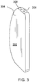
- FIG. 3 is a perspective view of a battery, according to one embodiment of the present subject matter.
- the battery 304 of the present subject matter is substantially flat.
- Substantially flat batteries include a plurality of battery electrodes stacked together, and further assembled into a battery case.
- Various battery cases are conductive or nonconductive.
- Some battery cases include feedthroughs 306, 308.
- an electrode of the battery is electrically connected to the case.
- the battery cases include a planar battery surface 302.
- the present subject matter includes, but is not limited to, embodiments disclosed at paragraphs 0095-0110, 0136-0196, 0206-0258 of the following related and commonly assigned U.S.
- FIG. 4 is a perspective view of an electronics module 404, according to one embodiment of the present subject matter.
- the electronics module 404 includes at least one face 408.
- the face is planar, although other face contours, such as curved contours, or other nonlinear contours, are possible without departing from the scope of the present subject matter. Accordingly, it should be noted that some electronics module 404 layers do not include a planar face, but instead include a face which is adapted to mate to another component in an implantable device.
- the present subject matter includes, but is not limited an electronics modules 404 which are, planar, flexible, folded, and/or nonplanar in various embodiments.
- the electronics module includes a face which a power source is interface with.
- the electronics face includes topography.
- the topography is substantially planar.
- the topography is nonplanar.
- a power source which interfaces with the topography is equidistant from the topography, when the distance is measured orthogonally away from the electronics face. In some embodiments, the distance from the electronics face to the interfacing power source varies depending on where the distance is measured.
- Some embodiments include one or more features which depart from a face of the electronics module 404. Some embodiments include one or more features which define an indentation in a face of the electronics module 404.
- the present subject matter includes, but is not limited to, embodiments in which a cylinder shape extends away from a face of the electronics module 404. Other embodiments exist, however, in which the feature is shaped otherwise. It should be noted that a feature does not necessarily exhibit a constant cross section along an axis extending away from a face orthogonally.
- a feature 402 which is a transformer.
- the electronics module 404 has a first thickness 4W, measured orthogonally away from a first planar face.
- the electronics module includes a feature which extends away from the first planar face a thickness of 4W2, measured orthogonally away from an electronics face.
- the second thickness 4W2 is less than the first thickness 4W.
- the second thickness is greater than the first thickness 4W.
- the first thickness 4W is substantially equivalent to the second thickness 4W2.
- Embodiments are contemplated in which multiple features extend away from one or more faces at equivalent thicknesses.
- Embodiments are additionally contemplated in which multiple features extend away from one or more faces at different thicknesses.
- a plate which is shaped to match face 408 is adapted to accommodate feature 402.
- some embodiments include a cut out which is adapted to receive feature 402.
- Some embodiments include a cut into the side of a layer to be mated to the electronics module 404. Additional embodiments include a cut-out which is inside the overall perimeter of the layer to be matted the electronics module 404.
- the present subject matter is not limited to embodiments in which the electronics module 404 has a major face 408 on which a feature 402 is located, as other configurations, including configuration in which a feature does not extend from a substantially planar face, are within the scope of the present subject matter.
- FIG. 5 is a perspective view of electronics and a power source, according to one embodiment of the present subject matter.
- the electronics 504 are mated to a power source 510.
- two components are in a stack 500 and are mated along an interface 508.
- the electronics include a feature 502.
- the feature 502 is a transformer.
- the power source 510 includes a void 506 which is adapted to receive the feature 502 while the power source 510 and the electronics 504 are in a stack 500.
- the power source 510 is a battery. In some embodiments, the power source 510 is a capacitor. In various embodiments, the power source 510 includes a stack of substantially planar layers which are shaped to define the void 506. Although a power source 510 is illustrated which exhibits a consistent cross section as it extends away from interface 508, the present subject matter is not so limited. The present subject matter includes other power source shapes which do not include a constant cross section as the power source extends away from interface 508 orthogonally.
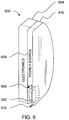
- FIG. 6 is a perspective view of electronics and a power source, according to one embodiment of the present subject matter.
- the electronics 604 are mated to a power source 610.
- two components are in a stack 600 and are mated along an interface 608.
- the electronics include a feature 602.
- the feature 602 is a transformer.
- the power source 610 includes a void 606 which is adapted to receive the feature 602 while the power source 610 and the electronics 604 are in a stack 600.
- the power source 610 is a battery. In some embodiments, the power source 610 is a capacitor. In various embodiments, the power source 610 includes a stack of substantially planar layers which are shaped to define the void 606. Although a power source 610 is illustrated which exhibits a consistent cross section as it extends away from interface 608, the present subject matter is not so limited. The present subject matter includes other power source shapes which do not include a constant cross section as the power source extends away from interface 608 orthogonally.
- the present illustrations shows a power source which does not have a uniform cross section as it extends orthogonally away from the interface 608.
- the illustrated power source 610 includes a shelf 612 which extends over the feature 602 and which opposes portions of electronics 604 which are under and which support feature 602.
- the power source 608 includes a stack of substantially planar layers. In various embodiments, these layers are shaped differently to define void 606. at least one or more of the layers of the power source define shelf 602, in various embodiments.
- the present subject matter allows for an adjustable thickness power source 610 which can accommodate one or more features simply by stacking more or less electrode layers, and providing a case for those electrode layers which is shaped to accommodate those layers.
- a process includes establishing form factor and power capacity requirements for a power source to be used in an implantable medical device.
- the embodiment includes constructing a flat battery by stacking flat battery layers into a battery stack and positioning the stack in a battery case with a planar interface and a battery perimeter and battery thickness.
- the embodiment further includes constructing a flat electrolytic capacitor by stacking flat capacitor layers into a capacitor stack and positioning the stack in a capacitor case with a planar interface and a capacitor perimeter and capacitor thickness.
- the embodiment additionally includes layers the flat battery and the flat electrolytic capacitor with an electronics module.
- Embodiments are included in which a battery perimeter is substantially coextensive with an electronics module perimeter.
- Embodiments are additionally contemplated in which a capacitor perimeter is substantially coextensive with an electronics module perimeter.
- Embodiments are included which encapsulate the stack with at least a first housing portion and a second housing portion.
- the first housing portion opposes the second housing portion.
- the first housing portion is a cup
- the second housing portion is a lid.
- the first housing portion is a cup with a first cup mouth
- the second housing portion is a cup with a second cup mouth.
- the first cup mouth conforms to the second cup mouth and is sealed to the second cup mouth with a seal.
- a seal includes a laser weld, in various embodiments. The laser weld occurs at a butt joint, a step joint, a lap joint, and/or other joints, in various embodiments. In various embodiments, the seal is hermetic.
- the first housing portion and the second housing portion at least partially define an interior.
- the battery, capacitor, and electronics module are disposed in the interior.
- additional components are disposed in the interior.
- the first housing portion is trimmed based on a thickness of a stack disposed in the interior.
- the stack includes the battery, the capacitor, and the electronics module, stack unto one another.
- the battery and the capacitor sandwich the electronics module.
- the stack is composed of components which are layered onto one another along a vector which runs orthogonally between the first housing portion and the second housing portion.
- the vector is orthogonal to an first interior face of the first housing portion, and a second interior face of the second housing.
- the first interior face is substantially planar.
- the second interior face is substantially planar.
- the second housing portion is trimmed. In various embodiments, both the first and second housing portions are trimmed.
- a battery thickness, battery perimeter, capacitor thickness and capacitor perimeter are selected based on form factor and power capacity requirements for an implantable medical device. Additionally, various method embodiments include measuring a ratio between battery thickness and capacitor thickness, and using this ratio in selecting a battery and capacitor. A ratio is be established by known power requirements, in various embodiments. Another example combines size requirements with power requirements in selecting a ratio. The ratio can be stored and used by a design process or manufacturing process to discern the mechanical and electrical composition of a needed power source, in various embodiments.
- the present subject matter includes delivering from the flat battery and the flat electrolytic capacitor from about 1.25 Joules per Amp hour of battery capacity to about 50 Joules per amp hour of battery capacity.
- the flat battery has a battery capacity density of from about 0.23 amp hours per cubic centimeter of flat battery to about 0.25 amp hours per cubic centimeter of flat battery. Battery capacity density is measured by dividing the amp-hour rating of the battery by the battery volume, in various embodiments.
- the present subject matter includes, but is not limited to, embodiments disclosed at paragraphs 0095-0110, 0136-0196, 0206-0258 of the following related and commonly assigned U.S. Patent Publication, "Batteries Including a Flat Plate Design," U.S.
- the flat electrolytic capacitor includes an energy density of from about 4.65 joules per cubic centimeter of flat electrolytic capacitor to 6.5 joules per cubic centimeter of flat electrolytic capacitor.
- the present subject matter includes, but is not limited to, embodiments disclosed on or around pages 12-37, 39, 41-140 of the following related and commonly assigned Provisional U.S. Patent Application "Method and Apparatus for Single High Voltage Aluminum Capacitor Design," Ser. No. 60/588,905, filed on July 16, 2004 , and published as US2006/0023400 A1 .
- Embodiments are contemplated in which a power source form factor is known, and in which a device housing is trimmed to fit the power source form factor.
- a performance specification requires a predetermined number of capacitor electrodes to be stacked into a power source and then stacked onto an electronics module.
- Some embodiments include a performance specification which requires a predetermined number of battery electrodes to be stacked into a power source and then onto an electronics module.
- a process is able to determine the overall thickness of one or more power sources, combined with an electronics module.
- the present subject matter tailors a device housing to this overall thickness. In some of these embodiments, this is done by drawing one or more housing portions, and then trimming these housing portions. Because of the nature of a drawing process, various embodiments are able to provide housings of different depths with reduced tooling expenses. A further benefit is a reduced time to retool. Another benefit is the provision of a retooling process which provides improved adjustability.
- electrode machinery is tooled to form an electrode of a specific size and shape.
- a substantially planar electrode is punched out of a sheet.
- the sheet is on a roll.
- Batteries and capacitors of different capacities require more or less surface area.
- One way to add surface area is to increase a punch perimeter of an electrode.
- Such changes to tooling can be cost intensive, therefore it is beneficial to pursue an alternative route to increasing surface area.
- One alternative is to increase the number of layers in a stack.
- the present subject matter allows for easy adjustment to stack height by enabling device housing changes which can accommodate a range of stack heights with reduced tooling changes.
- a power source capacity is increased by adding layers to a stack of that power source.
- various embodiments change the trim height of a device housing.
- the device housing can be made deeper by using the same workpiece which is a product of a drawing operation, and changing the height at which the workpiece is trimmed.
- the number of capacitor foil layers are reduced.
- the number of battery electrode layers are increased. The device housing does not have to be adjusted to accommodate the changes.
- a single two-axis machine can position capacitor layers in a stack, position the capacitor stack in a capacitor case, position battery layers in a stack, and position the battery stack in a battery case.
- the single two-axis machine is a pick-and-place machine. This combination is provided for illustration, but other combinations of these steps are possible, and additional steps are also within the scope of the present subject matter.
Landscapes
- Health & Medical Sciences (AREA)
- Public Health (AREA)
- Chemical & Material Sciences (AREA)
- Nuclear Medicine, Radiotherapy & Molecular Imaging (AREA)
- Radiology & Medical Imaging (AREA)
- Life Sciences & Earth Sciences (AREA)
- Animal Behavior & Ethology (AREA)
- Biomedical Technology (AREA)
- General Health & Medical Sciences (AREA)
- Veterinary Medicine (AREA)
- Engineering & Computer Science (AREA)
- Chemical Kinetics & Catalysis (AREA)
- Electrochemistry (AREA)
- General Chemical & Material Sciences (AREA)
- Battery Mounting, Suspending (AREA)
- Electrotherapy Devices (AREA)
- Electric Double-Layer Capacitors Or The Like (AREA)
Applications Claiming Priority (2)
| Application Number | Priority Date | Filing Date | Title |
|---|---|---|---|
| US11/467,808 US8874214B2 (en) | 2006-08-28 | 2006-08-28 | Implantable pulse generator with a stacked capacitor, battery, and electronics |
| PCT/US2007/070697 WO2008027639A2 (en) | 2006-08-28 | 2007-06-08 | Device with stacked capacitor, battery, and electronics |
Publications (2)
| Publication Number | Publication Date |
|---|---|
| EP2056930A2 EP2056930A2 (en) | 2009-05-13 |
| EP2056930B1 true EP2056930B1 (en) | 2018-01-10 |
Family
ID=39060334
Family Applications (1)
| Application Number | Title | Priority Date | Filing Date |
|---|---|---|---|
| EP07798278.3A Not-in-force EP2056930B1 (en) | 2006-08-28 | 2007-06-08 | Device with stacked capacitor, battery, and electronics |
Country Status (4)
| Country | Link |
|---|---|
| US (1) | US8874214B2 (enExample) |
| EP (1) | EP2056930B1 (enExample) |
| JP (1) | JP5089698B2 (enExample) |
| WO (1) | WO2008027639A2 (enExample) |
Families Citing this family (26)
| Publication number | Priority date | Publication date | Assignee | Title |
|---|---|---|---|---|
| WO2004052182A2 (en) * | 2002-12-11 | 2004-06-24 | Proteus Biomedical, Inc. | Monitoring and treating hemodynamic parameters |
| US7204798B2 (en) * | 2003-01-24 | 2007-04-17 | Proteus Biomedical, Inc. | Methods and systems for measuring cardiac parameters |
| US7214189B2 (en) * | 2004-09-02 | 2007-05-08 | Proteus Biomedical, Inc. | Methods and apparatus for tissue activation and monitoring |
| WO2006105474A2 (en) * | 2005-03-31 | 2006-10-05 | Proteus Biomedical, Inc. | Automated optimization of multi-electrode pacing for cardiac resynchronization |
| US20060247715A1 (en) * | 2005-04-29 | 2006-11-02 | Youker Nick A | Method and apparatus for an implantable pulse generator with a stacked battery and capacitor |
| EP1898999A4 (en) * | 2005-07-01 | 2011-10-19 | Proteus Biomedical Inc | INSERTABLE EPICARDIAL ELECTRODE AND SENSOR ARRANGEMENT |
| US7571006B2 (en) | 2005-07-15 | 2009-08-04 | Brian Gordon | Wearable alarm system for a prosthetic hearing implant |
| WO2007021804A2 (en) * | 2005-08-12 | 2007-02-22 | Proteus Biomedical, Inc. | Evaluation of depolarization wave conduction velocity |
| JP2009521276A (ja) * | 2005-12-22 | 2009-06-04 | プロテウス バイオメディカル インコーポレイテッド | 植え込み型集積回路 |
| WO2007098202A2 (en) | 2006-02-16 | 2007-08-30 | Imthera Medical, Inc. | An rfid based apparatus, system, and method for therapeutic treatment of a patient |
| US8874214B2 (en) | 2006-08-28 | 2014-10-28 | Cardiac Pacemakers, Inc. | Implantable pulse generator with a stacked capacitor, battery, and electronics |
| AU2008311313A1 (en) | 2007-10-09 | 2009-04-16 | Imthera Medical, Inc. | System and method for neural stimulation |
| WO2009131749A2 (en) * | 2008-02-28 | 2009-10-29 | Proteus Biomedical, Inc. | Integrated circuit implementation and fault control system, device, and method |
| US20090287266A1 (en) * | 2008-05-13 | 2009-11-19 | Mark Zdeblick | High-voltage tolerant multiplex multi-electrode stimulation systems and methods for using the same |
| US8428725B2 (en) * | 2008-10-09 | 2013-04-23 | Imthera Medical, Inc. | Method of stimulating a Hypoglossal nerve for controlling the position of a patient's tongue |
| JP2012508627A (ja) * | 2008-11-13 | 2012-04-12 | プロテウス バイオメディカル インコーポレイテッド | ペーシングおよび刺激システム、デバイス、および方法 |
| US8644919B2 (en) | 2008-11-13 | 2014-02-04 | Proteus Digital Health, Inc. | Shielded stimulation and sensing system and method |
| JP2012508624A (ja) * | 2008-11-13 | 2012-04-12 | プロテウス バイオメディカル インコーポレイテッド | 多重化複数電極神経刺激装置 |
| WO2010065465A2 (en) * | 2008-12-02 | 2010-06-10 | Proteus Biomedical, Inc. | Analyzer compatible communication protocol |
| US20110082530A1 (en) * | 2009-04-02 | 2011-04-07 | Mark Zdeblick | Method and Apparatus for Implantable Lead |
| US8786049B2 (en) | 2009-07-23 | 2014-07-22 | Proteus Digital Health, Inc. | Solid-state thin-film capacitor |
| BR112012010986A2 (pt) | 2009-11-10 | 2016-04-12 | Imthera Medical Inc | sistema para estimular um nervo hipoglosso para o controle da posição da língua de um paciente |
| US8718770B2 (en) | 2010-10-21 | 2014-05-06 | Medtronic, Inc. | Capture threshold measurement for selection of pacing vector |
| US8355784B2 (en) | 2011-05-13 | 2013-01-15 | Medtronic, Inc. | Dynamic representation of multipolar leads in a programmer interface |
| US20140275915A1 (en) | 2013-03-13 | 2014-09-18 | Medtronic, Inc. | Implantable medical device including a molded planar transformer |
| US9607759B2 (en) | 2013-03-13 | 2017-03-28 | Medtronic, Inc. | Implantable medical device including a molded planar transformer |
Family Cites Families (39)
| Publication number | Priority date | Publication date | Assignee | Title |
|---|---|---|---|---|
| US3993508A (en) | 1975-06-20 | 1976-11-23 | Polaroid Corporation | Method for manufacturing flat batteries |
| IL50024A (en) | 1976-07-12 | 1979-05-31 | Israel State | Secondary cells |
| US4254775A (en) * | 1979-07-02 | 1981-03-10 | Mieczyslaw Mirowski | Implantable defibrillator and package therefor |
| US5131388A (en) | 1991-03-14 | 1992-07-21 | Ventritex, Inc. | Implantable cardiac defibrillator with improved capacitors |
| JP2687785B2 (ja) | 1991-09-27 | 1997-12-08 | 日本電気株式会社 | 半導体記憶装置 |
| US5370663A (en) | 1993-08-12 | 1994-12-06 | Intermedics, Inc. | Implantable cardiac-stimulator with flat capacitor |
| US5370669A (en) | 1993-11-17 | 1994-12-06 | Intermedics, Inc. | Implantable cardiac defibrillator with layered package |
| US5522851A (en) | 1994-12-06 | 1996-06-04 | Ventritex, Inc. | Capacitor for an implantable cardiac defibrillator |
| US5749911A (en) | 1997-01-24 | 1998-05-12 | Cardiac Pacemakers, Inc. | Implantable tissue stimulator incorporating deposited multilayer capacitor |
| US6330925B1 (en) | 1997-01-31 | 2001-12-18 | Ovonic Battery Company, Inc. | Hybrid electric vehicle incorporating an integrated propulsion system |
| US6185452B1 (en) | 1997-02-26 | 2001-02-06 | Joseph H. Schulman | Battery-powered patient implantable device |
| US5954751A (en) | 1998-01-15 | 1999-09-21 | Intermedics Inc. | Implantable defibrillator with stacked transistor subassemblies |
| US6445948B1 (en) | 1998-04-03 | 2002-09-03 | Medtronic, Inc. | Implantable medical device having a substantially flat battery |
| US6388866B1 (en) | 1998-04-03 | 2002-05-14 | Medtronic, Inc. | Implantable medical device having flat electrolytic capacitor with tailored anode layers |
| US6459566B1 (en) | 1998-06-24 | 2002-10-01 | Medtronic, Inc. | Implantable medical device having flat electrolytic capacitor with laser welded cover |
| US6010317A (en) | 1998-09-01 | 2000-01-04 | Baxter International Inc. | Electrochemical cell module having an inner and an outer shell with a nested arrangement |
| US6556863B1 (en) | 1998-10-02 | 2003-04-29 | Cardiac Pacemakers, Inc. | High-energy capacitors for implantable defibrillators |
| US6678559B1 (en) | 1999-03-23 | 2004-01-13 | Medtronic, Inc. | Implantable medical device having a capacitor assembly with liner |
| US7110240B2 (en) | 2000-03-20 | 2006-09-19 | Medtronic, Inc. | Implantable medical device having flat electrolytic capacitor with differing sized anode and cathode layers |
| US6498951B1 (en) | 2000-10-13 | 2002-12-24 | Medtronic, Inc. | Implantable medical device employing integral housing for a formable flat battery |
| US6509588B1 (en) * | 2000-11-03 | 2003-01-21 | Cardiac Pacemakers, Inc. | Method for interconnecting anodes and cathodes in a flat capacitor |
| US6833987B1 (en) | 2000-11-03 | 2004-12-21 | Cardiac Pacemakers, Inc. | Flat capacitor having an active case |
| US6571126B1 (en) | 2000-11-03 | 2003-05-27 | Cardiac Pacemakers, Inc. | Method of constructing a capacitor stack for a flat capacitor |
| US6522525B1 (en) | 2000-11-03 | 2003-02-18 | Cardiac Pacemakers, Inc. | Implantable heart monitors having flat capacitors with curved profiles |
| US6699265B1 (en) | 2000-11-03 | 2004-03-02 | Cardiac Pacemakers, Inc. | Flat capacitor for an implantable medical device |
| US6782290B2 (en) | 2001-04-27 | 2004-08-24 | Medtronic, Inc. | Implantable medical device with rechargeable thin-film microbattery power source |
| US6721602B2 (en) | 2001-08-21 | 2004-04-13 | Medtronic, Inc. | Implantable medical device assembly and manufacturing method |
| KR20040082422A (ko) | 2002-02-12 | 2004-09-24 | 에버레디 배터리 컴퍼니, 인크. | 가요성의 얇은 인쇄 전지 및 장치와 그것의 제조 방법 |
| US6799072B2 (en) | 2002-04-25 | 2004-09-28 | Medtronic, Inc. | Electrically insulated component sub-assemblies of implantable medical devices |
| US6881516B2 (en) | 2002-09-30 | 2005-04-19 | Medtronic, Inc. | Contoured battery for implantable medical devices and method of manufacture |
| DE10247674A1 (de) | 2002-10-09 | 2004-04-22 | Biotronik Meß- und Therapiegeräte GmbH & Co. Ingenieurbüro Berlin | Elektromedizinisches Implantat zur interkardialen Herztherapie |
| US7479349B2 (en) | 2002-12-31 | 2009-01-20 | Cardiac Pacemakers, Inc. | Batteries including a flat plate design |
| US8691418B2 (en) | 2003-02-07 | 2014-04-08 | Cardiac Pacemakers, Inc. | Insulative member on battery cathode |
| US20040220627A1 (en) | 2003-04-30 | 2004-11-04 | Crespi Ann M. | Complex-shaped ceramic capacitors for implantable cardioverter defibrillators and method of manufacture |
| US20050154423A1 (en) | 2004-01-13 | 2005-07-14 | Goedeke Steven D. | Method for reducing implantable defibrillator volume |
| US7180727B2 (en) | 2004-07-16 | 2007-02-20 | Cardiac Pacemakers, Inc. | Capacitor with single sided partial etch and stake |
| US7224575B2 (en) | 2004-07-16 | 2007-05-29 | Cardiac Pacemakers, Inc. | Method and apparatus for high voltage aluminum capacitor design |
| US20060247715A1 (en) | 2005-04-29 | 2006-11-02 | Youker Nick A | Method and apparatus for an implantable pulse generator with a stacked battery and capacitor |
| US8874214B2 (en) | 2006-08-28 | 2014-10-28 | Cardiac Pacemakers, Inc. | Implantable pulse generator with a stacked capacitor, battery, and electronics |
-
2006
- 2006-08-28 US US11/467,808 patent/US8874214B2/en not_active Expired - Fee Related
-
2007
- 2007-06-08 WO PCT/US2007/070697 patent/WO2008027639A2/en not_active Ceased
- 2007-06-08 JP JP2009526779A patent/JP5089698B2/ja not_active Expired - Fee Related
- 2007-06-08 EP EP07798278.3A patent/EP2056930B1/en not_active Not-in-force
Also Published As
| Publication number | Publication date |
|---|---|
| WO2008027639A2 (en) | 2008-03-06 |
| EP2056930A2 (en) | 2009-05-13 |
| WO2008027639A3 (en) | 2008-05-29 |
| JP5089698B2 (ja) | 2012-12-05 |
| US20080091246A1 (en) | 2008-04-17 |
| JP2010502295A (ja) | 2010-01-28 |
| US8874214B2 (en) | 2014-10-28 |
Similar Documents
| Publication | Publication Date | Title |
|---|---|---|
| EP2056930B1 (en) | Device with stacked capacitor, battery, and electronics | |
| US7917207B2 (en) | Method and apparatus for an implantable pulse generator with a stacked battery and capacitor | |
| US11837690B2 (en) | Battery pack for a cordless power tool | |
| KR100965049B1 (ko) | 고출력 리튬 2차 전지 유닛셀의 적층 구조 | |
| US9225034B2 (en) | Stepwise electrode assembly having variously-shaped corner and secondary battery, battery pack and device comprising the same | |
| US9968792B2 (en) | Implantable medical device housing having integrated features | |
| KR101403388B1 (ko) | 비정형 구조의 전지셀 및 이를 포함하는 전지모듈 | |
| KR101443832B1 (ko) | 이차전지 케이스 제조장치 및 제조 방법 | |
| KR102323905B1 (ko) | 전기화학적 다중셀 및 이를 위한 방법 | |
| KR101467859B1 (ko) | 이차전지용 전지케이스 | |
| EP2846392B1 (en) | Electrode assembly, and battery and device comprising same | |
| KR20200053463A (ko) | 전기화학적 셀을 위한 적층된 각기둥형 아키텍처 | |
| EP3275030B1 (en) | Adjustable battery stack and method of use in device enclosure | |
| WO2019131503A1 (ja) | 全固体電池、その製造方法および加工装置 | |
| KR20140100032A (ko) | 단차 구조를 포함하는 전지셀 | |
| KR102646788B1 (ko) | 곡률을 갖는 3차원 구조의 이차전지 및 그 제조방법 | |
| EP3279968B1 (en) | Battery module | |
| EP3793015A1 (en) | Icb assembly, battery module including same, and manufacturing method therefor | |
| EP1886327A1 (en) | Insulative film for electrolytic capacitors | |
| KR20150133165A (ko) | 단차 구조를 포함하는 전지셀 | |
| CN115428236B (zh) | 电池单元的制造方法和袋成形设备 | |
| US20250286175A1 (en) | Secondary battery, and device and method for manufacturing secondary battery | |
| US20250337003A1 (en) | Battery and method for manufacturing the battery | |
| KR20240047899A (ko) | 이차전지, 그 이차전지의 제조방법, 및 그 제조방법에 이용되는 가압장치 | |
| EP1643582A1 (en) | Method of fabricating rechargeable batteries |
Legal Events
| Date | Code | Title | Description |
|---|---|---|---|
| PUAI | Public reference made under article 153(3) epc to a published international application that has entered the european phase |
Free format text: ORIGINAL CODE: 0009012 |
|
| 17P | Request for examination filed |
Effective date: 20090317 |
|
| AK | Designated contracting states |
Kind code of ref document: A2 Designated state(s): AT BE BG CH CY CZ DE DK EE ES FI FR GB GR HU IE IS IT LI LT LU LV MC MT NL PL PT RO SE SI SK TR |
|
| AX | Request for extension of the european patent |
Extension state: AL BA HR MK RS |
|
| DAX | Request for extension of the european patent (deleted) | ||
| STAA | Information on the status of an ep patent application or granted ep patent |
Free format text: STATUS: EXAMINATION IS IN PROGRESS |
|
| 17Q | First examination report despatched |
Effective date: 20170124 |
|
| GRAP | Despatch of communication of intention to grant a patent |
Free format text: ORIGINAL CODE: EPIDOSNIGR1 |
|
| STAA | Information on the status of an ep patent application or granted ep patent |
Free format text: STATUS: GRANT OF PATENT IS INTENDED |
|
| INTG | Intention to grant announced |
Effective date: 20170802 |
|
| GRAS | Grant fee paid |
Free format text: ORIGINAL CODE: EPIDOSNIGR3 |
|
| GRAA | (expected) grant |
Free format text: ORIGINAL CODE: 0009210 |
|
| STAA | Information on the status of an ep patent application or granted ep patent |
Free format text: STATUS: THE PATENT HAS BEEN GRANTED |
|
| AK | Designated contracting states |
Kind code of ref document: B1 Designated state(s): AT BE BG CH CY CZ DE DK EE ES FI FR GB GR HU IE IS IT LI LT LU LV MC MT NL PL PT RO SE SI SK TR |
|
| REG | Reference to a national code |
Ref country code: GB Ref legal event code: FG4D |
|
| REG | Reference to a national code |
Ref country code: CH Ref legal event code: EP Ref country code: AT Ref legal event code: REF Ref document number: 961742 Country of ref document: AT Kind code of ref document: T Effective date: 20180115 |
|
| REG | Reference to a national code |
Ref country code: IE Ref legal event code: FG4D |
|
| REG | Reference to a national code |
Ref country code: DE Ref legal event code: R096 Ref document number: 602007053703 Country of ref document: DE |
|
| REG | Reference to a national code |
Ref country code: NL Ref legal event code: FP |
|
| REG | Reference to a national code |
Ref country code: FR Ref legal event code: PLFP Year of fee payment: 12 |
|
| REG | Reference to a national code |
Ref country code: AT Ref legal event code: MK05 Ref document number: 961742 Country of ref document: AT Kind code of ref document: T Effective date: 20180110 |
|
| PG25 | Lapsed in a contracting state [announced via postgrant information from national office to epo] |
Ref country code: FI Free format text: LAPSE BECAUSE OF FAILURE TO SUBMIT A TRANSLATION OF THE DESCRIPTION OR TO PAY THE FEE WITHIN THE PRESCRIBED TIME-LIMIT Effective date: 20180110 Ref country code: LT Free format text: LAPSE BECAUSE OF FAILURE TO SUBMIT A TRANSLATION OF THE DESCRIPTION OR TO PAY THE FEE WITHIN THE PRESCRIBED TIME-LIMIT Effective date: 20180110 Ref country code: ES Free format text: LAPSE BECAUSE OF FAILURE TO SUBMIT A TRANSLATION OF THE DESCRIPTION OR TO PAY THE FEE WITHIN THE PRESCRIBED TIME-LIMIT Effective date: 20180110 Ref country code: CY Free format text: LAPSE BECAUSE OF FAILURE TO SUBMIT A TRANSLATION OF THE DESCRIPTION OR TO PAY THE FEE WITHIN THE PRESCRIBED TIME-LIMIT Effective date: 20180110 |
|
| PG25 | Lapsed in a contracting state [announced via postgrant information from national office to epo] |
Ref country code: BG Free format text: LAPSE BECAUSE OF FAILURE TO SUBMIT A TRANSLATION OF THE DESCRIPTION OR TO PAY THE FEE WITHIN THE PRESCRIBED TIME-LIMIT Effective date: 20180410 Ref country code: GR Free format text: LAPSE BECAUSE OF FAILURE TO SUBMIT A TRANSLATION OF THE DESCRIPTION OR TO PAY THE FEE WITHIN THE PRESCRIBED TIME-LIMIT Effective date: 20180411 Ref country code: PL Free format text: LAPSE BECAUSE OF FAILURE TO SUBMIT A TRANSLATION OF THE DESCRIPTION OR TO PAY THE FEE WITHIN THE PRESCRIBED TIME-LIMIT Effective date: 20180110 Ref country code: IS Free format text: LAPSE BECAUSE OF FAILURE TO SUBMIT A TRANSLATION OF THE DESCRIPTION OR TO PAY THE FEE WITHIN THE PRESCRIBED TIME-LIMIT Effective date: 20180510 Ref country code: SE Free format text: LAPSE BECAUSE OF FAILURE TO SUBMIT A TRANSLATION OF THE DESCRIPTION OR TO PAY THE FEE WITHIN THE PRESCRIBED TIME-LIMIT Effective date: 20180110 Ref country code: LV Free format text: LAPSE BECAUSE OF FAILURE TO SUBMIT A TRANSLATION OF THE DESCRIPTION OR TO PAY THE FEE WITHIN THE PRESCRIBED TIME-LIMIT Effective date: 20180110 Ref country code: AT Free format text: LAPSE BECAUSE OF FAILURE TO SUBMIT A TRANSLATION OF THE DESCRIPTION OR TO PAY THE FEE WITHIN THE PRESCRIBED TIME-LIMIT Effective date: 20180110 |
|
| REG | Reference to a national code |
Ref country code: DE Ref legal event code: R097 Ref document number: 602007053703 Country of ref document: DE |
|
| PG25 | Lapsed in a contracting state [announced via postgrant information from national office to epo] |
Ref country code: EE Free format text: LAPSE BECAUSE OF FAILURE TO SUBMIT A TRANSLATION OF THE DESCRIPTION OR TO PAY THE FEE WITHIN THE PRESCRIBED TIME-LIMIT Effective date: 20180110 Ref country code: RO Free format text: LAPSE BECAUSE OF FAILURE TO SUBMIT A TRANSLATION OF THE DESCRIPTION OR TO PAY THE FEE WITHIN THE PRESCRIBED TIME-LIMIT Effective date: 20180110 |
|
| PLBE | No opposition filed within time limit |
Free format text: ORIGINAL CODE: 0009261 |
|
| STAA | Information on the status of an ep patent application or granted ep patent |
Free format text: STATUS: NO OPPOSITION FILED WITHIN TIME LIMIT |
|
| PG25 | Lapsed in a contracting state [announced via postgrant information from national office to epo] |
Ref country code: CZ Free format text: LAPSE BECAUSE OF FAILURE TO SUBMIT A TRANSLATION OF THE DESCRIPTION OR TO PAY THE FEE WITHIN THE PRESCRIBED TIME-LIMIT Effective date: 20180110 Ref country code: SK Free format text: LAPSE BECAUSE OF FAILURE TO SUBMIT A TRANSLATION OF THE DESCRIPTION OR TO PAY THE FEE WITHIN THE PRESCRIBED TIME-LIMIT Effective date: 20180110 Ref country code: DK Free format text: LAPSE BECAUSE OF FAILURE TO SUBMIT A TRANSLATION OF THE DESCRIPTION OR TO PAY THE FEE WITHIN THE PRESCRIBED TIME-LIMIT Effective date: 20180110 |
|
| 26N | No opposition filed |
Effective date: 20181011 |
|
| REG | Reference to a national code |
Ref country code: CH Ref legal event code: PL |
|
| PG25 | Lapsed in a contracting state [announced via postgrant information from national office to epo] |
Ref country code: SI Free format text: LAPSE BECAUSE OF FAILURE TO SUBMIT A TRANSLATION OF THE DESCRIPTION OR TO PAY THE FEE WITHIN THE PRESCRIBED TIME-LIMIT Effective date: 20180110 |
|
| REG | Reference to a national code |
Ref country code: BE Ref legal event code: MM Effective date: 20180630 |
|
| REG | Reference to a national code |
Ref country code: IE Ref legal event code: MM4A |
|
| PG25 | Lapsed in a contracting state [announced via postgrant information from national office to epo] |
Ref country code: LU Free format text: LAPSE BECAUSE OF NON-PAYMENT OF DUE FEES Effective date: 20180608 Ref country code: MC Free format text: LAPSE BECAUSE OF FAILURE TO SUBMIT A TRANSLATION OF THE DESCRIPTION OR TO PAY THE FEE WITHIN THE PRESCRIBED TIME-LIMIT Effective date: 20180110 |
|
| PG25 | Lapsed in a contracting state [announced via postgrant information from national office to epo] |
Ref country code: CH Free format text: LAPSE BECAUSE OF NON-PAYMENT OF DUE FEES Effective date: 20180630 Ref country code: LI Free format text: LAPSE BECAUSE OF NON-PAYMENT OF DUE FEES Effective date: 20180630 Ref country code: IE Free format text: LAPSE BECAUSE OF NON-PAYMENT OF DUE FEES Effective date: 20180608 |
|
| PG25 | Lapsed in a contracting state [announced via postgrant information from national office to epo] |
Ref country code: BE Free format text: LAPSE BECAUSE OF NON-PAYMENT OF DUE FEES Effective date: 20180630 |
|
| PG25 | Lapsed in a contracting state [announced via postgrant information from national office to epo] |
Ref country code: MT Free format text: LAPSE BECAUSE OF NON-PAYMENT OF DUE FEES Effective date: 20180608 |
|
| PG25 | Lapsed in a contracting state [announced via postgrant information from national office to epo] |
Ref country code: TR Free format text: LAPSE BECAUSE OF FAILURE TO SUBMIT A TRANSLATION OF THE DESCRIPTION OR TO PAY THE FEE WITHIN THE PRESCRIBED TIME-LIMIT Effective date: 20180110 |
|
| PG25 | Lapsed in a contracting state [announced via postgrant information from national office to epo] |
Ref country code: HU Free format text: LAPSE BECAUSE OF FAILURE TO SUBMIT A TRANSLATION OF THE DESCRIPTION OR TO PAY THE FEE WITHIN THE PRESCRIBED TIME-LIMIT; INVALID AB INITIO Effective date: 20070608 Ref country code: PT Free format text: LAPSE BECAUSE OF FAILURE TO SUBMIT A TRANSLATION OF THE DESCRIPTION OR TO PAY THE FEE WITHIN THE PRESCRIBED TIME-LIMIT Effective date: 20180110 |
|
| PGFP | Annual fee paid to national office [announced via postgrant information from national office to epo] |
Ref country code: FR Payment date: 20200512 Year of fee payment: 14 Ref country code: DE Payment date: 20200527 Year of fee payment: 14 |
|
| PGFP | Annual fee paid to national office [announced via postgrant information from national office to epo] |
Ref country code: GB Payment date: 20200527 Year of fee payment: 14 Ref country code: NL Payment date: 20200615 Year of fee payment: 14 Ref country code: IT Payment date: 20200512 Year of fee payment: 14 |
|
| REG | Reference to a national code |
Ref country code: DE Ref legal event code: R119 Ref document number: 602007053703 Country of ref document: DE |
|
| REG | Reference to a national code |
Ref country code: NL Ref legal event code: MM Effective date: 20210701 |
|
| GBPC | Gb: european patent ceased through non-payment of renewal fee |
Effective date: 20210608 |
|
| PG25 | Lapsed in a contracting state [announced via postgrant information from national office to epo] |
Ref country code: GB Free format text: LAPSE BECAUSE OF NON-PAYMENT OF DUE FEES Effective date: 20210608 Ref country code: DE Free format text: LAPSE BECAUSE OF NON-PAYMENT OF DUE FEES Effective date: 20220101 |
|
| PG25 | Lapsed in a contracting state [announced via postgrant information from national office to epo] |
Ref country code: NL Free format text: LAPSE BECAUSE OF NON-PAYMENT OF DUE FEES Effective date: 20210701 Ref country code: FR Free format text: LAPSE BECAUSE OF NON-PAYMENT OF DUE FEES Effective date: 20210630 |
|
| PG25 | Lapsed in a contracting state [announced via postgrant information from national office to epo] |
Ref country code: IT Free format text: LAPSE BECAUSE OF NON-PAYMENT OF DUE FEES Effective date: 20210608 |