EP2053665A2 - Process testers and testing methodology for thin-film photovoltaic devices - Google Patents
Process testers and testing methodology for thin-film photovoltaic devices Download PDFInfo
- Publication number
- EP2053665A2 EP2053665A2 EP08167335A EP08167335A EP2053665A2 EP 2053665 A2 EP2053665 A2 EP 2053665A2 EP 08167335 A EP08167335 A EP 08167335A EP 08167335 A EP08167335 A EP 08167335A EP 2053665 A2 EP2053665 A2 EP 2053665A2
- Authority
- EP
- European Patent Office
- Prior art keywords
- layer
- groove
- transparent conductive
- conductive oxide
- oxide layer
- Prior art date
- Legal status (The legal status is an assumption and is not a legal conclusion. Google has not performed a legal analysis and makes no representation as to the accuracy of the status listed.)
- Withdrawn
Links
Images





Classifications
-
- H—ELECTRICITY
- H10—SEMICONDUCTOR DEVICES; ELECTRIC SOLID-STATE DEVICES NOT OTHERWISE PROVIDED FOR
- H10F—INORGANIC SEMICONDUCTOR DEVICES SENSITIVE TO INFRARED RADIATION, LIGHT, ELECTROMAGNETIC RADIATION OF SHORTER WAVELENGTH OR CORPUSCULAR RADIATION
- H10F71/00—Manufacture or treatment of devices covered by this subclass
-
- H—ELECTRICITY
- H10—SEMICONDUCTOR DEVICES; ELECTRIC SOLID-STATE DEVICES NOT OTHERWISE PROVIDED FOR
- H10P—GENERIC PROCESSES OR APPARATUS FOR THE MANUFACTURE OR TREATMENT OF DEVICES COVERED BY CLASS H10
- H10P74/00—Testing or measuring during manufacture or treatment of wafers, substrates or devices
Definitions
- Embodiments of the present invention generally relate to photovoltaic devices and fabrication processes thereof.
- embodiments of the present invention relate to process testers, methods of manufacturing process testers, and testing methodology for thin-film photovoltaic devices.
- PV devices are devices that convert sunlight into direct current (DC) electrical power.
- a PV device may be classified as monocrystalline, polycrystalline, or thin-film depending on how the device is fabricated.
- Monocrystalline PV devices are produced by slicing wafers from a single crystal, high purity, silicon boule.
- Polycrystalline PV devices are produced by sawing a cast block of silicon into bars, then wafers.
- Thin-film PV devices are produced by depositing thin layers of materials, such as amorphous silicon, microcrystalline silicon or copper indium gallium selenide (CIGS), onto a suitable substrate.
- materials such as amorphous silicon, microcrystalline silicon or copper indium gallium selenide (CIGS)
- a method for forming a device for testing thin-film, photovoltaic production processes according to independent claims 1 and 5 a method for producing devices for testing thin-film, photovoltaic production processes according to independent claims 11 and 12, a method for determining thin-film, photovoltaic cell, tester or module process design rules according to independent claim 13, and a device for testing thin-film, photovoltaic production processes according to independent claims 6 and 10 are provided.
- the present invention generally provides process tester layouts defined by laser scribing, methodology for creating process testers, methodology of using process testers for solar line diagnostics, placement of process testers in PV module production, and methodology for creating design rule testers.
- a method for forming a device for testing thin-film, photovoltaic production processes comprises forming a front transparent conductive oxide layer over a substrate, laser scribing a groove in the front transparent conductive oxide layer in an isolation region of the device, forming an absorber layer over the front transparent conductive oxide layer, laser scribing a groove in the absorber layer in a first probe region of the device, laser scribing a groove in the absorber layer in a second probe region of the device, forming a back reflective layer over the absorber layer, laser scribing a groove in the back reflective layer in the isolation region of the device, and laser scribing a groove in the back reflective layer in a linking region of the device.
- the isolation region electrically isolates the device from adjacent photovoltaic structures.
- a method for forming a device for testing thin-film, photovoltaic production processes comprises forming a front transparent conductive oxide layer over a substrate, laser scribing a groove in the front transparent conductive oxide layer in an isolation region of the device, laser scribing a groove in the transparent conductive oxide layer across an outer and inner active region of the device, forming an absorber layer over the front transparent conductive oxide layer, laser scribing a groove in the absorber layer in the outer active region of the device prior, forming a back reflective layer over the absorber layer, laser scribing a groove in the back reflective layer in the isolation region of the device, and laser scribing a groove in the back reflective layer between the outer active region and the inner active region of the device.
- the isolation region electrically isolates the device from adjacent photovoltaic structures.
- a device for testing thin-film, photovoltaic production processes comprises a front transparent conductive oxide layer formed over a substrate, an absorber layer formed over the front transparent conductive oxide layer, and a back reflective layer formed over the absorber layer.
- the transparent conductive oxide layer has a groove in an isolation region of the device.
- the absorber layer has a groove in a first probe region of the device and a groove in a second probe region of the device.
- the back reflective layer has a groove in the isolation region of the device.
- the isolation region electrically isolates the device from adjacent photovoltaic structures.
- the back reflective layer has a groove in a linking region of the device.
- a device for testing thin-film, photovoltaic production processes comprises a front transparent conductive oxide layer formed over a substrate, an absorber layer formed over the front transparent conductive oxide layer, and a back reflective layer formed over the absorber layer, wherein.
- the transparent conductive oxide layer has a groove in an isolation region of the device and a groove across an outer and inner active region of the device.
- the absorber layer has a groove in the outer active region of the device.
- the back reflective layer has a groove in the isolation region of the device, the isolation region electrically isolates the device from adjacent photovoltaic structures, and the back reflective layer has a groove between the outer active region and the inner active region of the device.
- a method for producing devices for testing thin-film, photovoltaic production processes comprises forming a plurality of devices on a single substrate, wherein the devices are defined via laser scribing, wherein the plurality of devices is selected from the group consisting of a tester for measuring the contact resistance between a front transparent conductive oxide layer and a back reflective layer, a tester for measuring the back reflective layer sheet resistance, a tester for measuring the front transparent conductive oxide layer sheet resistance, and a tester for measuring diode characteristics, and wherein the location, position, and number of devices are manipulated and controlled during the production of photovoltaic modules.
- a method for producing devices for testing thin-film, photovoltaic production processes comprises forming a photovoltaic module on a substrate and forming a photovoltaic process tester on the substrate, wherein the tester is defined via laser scribing, wherein the tester is selected from the group consisting of a tester for measuring the contact resistance between a front transparent conductive oxide layer and a back reflective layer, a tester for measuring the back reflective layer sheet resistance, a tester for measuring the front transparent conductive oxide layer sheet resistance, and a tester for measuring diode characteristics, and wherein the tester is located in a cut area of the substrate.
- a method for determining thin-film, photovoltaic cell, tester or module process design rules comprises forming a plurality of photovoltaic cells and laser scribing grooves in each layer of the cells, wherein lateral distances between the grooves are varied to determine spacing for desired process characteristics.
- the photovoltaic cells comprise a transparent conductive oxide layer formed over a substrate, an absorber layer formed over the transparent conductive oxide layer, and a back reflective layer formed over the absorber layer.
- the invention is also directed to a device for carrying out the disclosed methods and including device parts for performing each described method steps. Furthermore, the invention is also directed to methods by which the described device operates. It includes method steps for carrying out every function of the device.
- Figure 1 is a schematic cross-section of a thin-film PV module showing series connections between individual cells.
- Figure 2 is a schematic cross-sectional view of an embodiment of a tester for measuring the contact resistance between a TCO layer and a back reflective layer.
- Figure 3 is a schematic cross-sectional view of an embodiment of a tester for measuring the sheet resistance in a back reflective layer.
- Figure 4 is a schematic cross-sectional view of an embodiment of a tester for measuring sheet resistance of a front TCO layer.
- Figure 5A is a schematic top view of a tester for performing diode measurements.
- Figure 5B is a schematic cross-sectional view of the tester in Figure 5A along line 5-5.
- Figure 6 is a schematic top view of an exemplary embodiment of groups of testers produced on a single substrate.
- Figure 7 is a schematic top view of four solar modules formed atop a single substrate.
- Figure 8 is a schematic cross-sectional view of an embodiment of the present invention comprising a test module having a series of cells with varied lateral spacing between insulating transparent conductive oxide layer grooves and absorber layer grooves.
- the present invention generally comprises process testers fabricated using standard PV device processes or standard photovoltaic cell processes.
- the present invention comprises process tester layouts defined by laser scribing, methodology for creating process testers, methodology of using process testers for solar line diagnostics, photovoltaic line diagnostics, placement of process testers in PV module production, and methodology for creating design rule testers.
- PV module 100 comprises a substrate 102, such as a glass or polymer substrate, with thin films formed thereover.
- a front transparent conducting oxide (TCO) layer 105 may be formed over the substrate 102.
- the TCO layer 105 may comprise tin oxide, zinc oxide, indium tin oxide, cadmium stannate, combinations thereof, or other suitable materials.
- a first insulating groove 112 may be created in the TCO layer 105 to interrupt lateral current flow.
- An absorber layer 115 may then be formed over the TCO layer 105.
- the absorber layer 115 may comprise layers of thin films, including but not limited to, amorphous silicon, microcrystalline silicon, copper indium gallium selenide (CIGS), or combinations thereof.
- a second laser scribing may create a groove 124 in the absorber layer 115, which may be filled during the subsequent step of forming a back reflective layer 125 over the absorber layer 115.
- the back reflective layer 125 may comprise a conductive layer and/or a reflective coating.
- the conductive layer may be a second TCO layer.
- the reflective coating may comprise metallic materials including, but not limited to Al, Ag, Ti, Cr, Au, Cu, Pt, alloys thereof, combinations thereof as well as other conductive and reflective materials.
- a second insulating groove 136 may be formed in the back reflective layer 125 to interrupt lateral current flow in the back reflective layer 125.
- each individual PV cell 101 of module 100 is electrically connected in series with each adjacent cell 101.
- Figure 1 depicts five PV cells 101 connected in series via the aforementioned laser scribing process; however, any number of PV cells 101 may be linked in this manner to form PV module 100.
- Embodiments of the present invention involve creating process testers by means of the same laser scribing processes used for creating and interconnecting PV cells 101 within PV module 100.
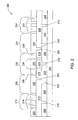
- FIG. 2 is a schematic cross-sectional view of an embodiment of a tester 200 for measuring the contact resistance between a TCO layer and a back reflective layer.
- the tester 200 comprises a substrate 202 with thin films formed thereover and divided into isolation regions 210, probe regions 220, and one or more linking regions 230.
- a front TCO layer 205 may be formed over the substrate 202.
- TCO insulating grooves 212, 222, and 232 may be created in the TCO layer 205, such that one or more grooves 212 are configured within each isolation region 210, one or more grooves 222 are configured within each probe region 220, and one or more grooves 232 are configured within each linking region 230.
- the lateral current in TCO layer 205 is interrupted by insulating grooves 212, 222, and 232.
- an absorber layer 215 may be formed over the TCO layer 205.
- grooves 224 and 234 may be created in absorber layer 215, such that one or more grooves 224 are configured within each probe region 220 and one or more grooves 234 are configured within each linking region 230. Although one or more grooves may be created in each isolation region 210 of the absorber layer 215, this is generally not necessary due to the low lateral conductivity of the absorber layer 215.
- a back reflective layer 225 may be formed over the absorber layer 215, such that electrical interconnection is established between the back reflective layer 225 and the TCO layer 205 at grooves 224 and 234.
- back reflective layer insulating grooves 216 and 236 may be created in the back reflective layer 225, such that one or more grooves 216 are configured within each isolation region 210 and one or more grooves 236 are configured within each linking region 230.
- lateral current in back reflective layer 225 is interrupted by insulating grooves 216 and 236.
- the resulting tester 200 comprises isolation regions 210, probe regions 220, and one or more linking regions 230.
- the isolation regions 210 electrically isolate the tester 200 from adjacent structures.
- An electrically interconnected chain is established between the probe regions 220 through the one or more linking regions 230, wherein conduction alternates between the back reflective layer 225 and the TCO layer 205.
- Figure 2 depicts one linking region 230, any number of linking regions 230 may be interconnected in the tester 200.
- electrical probes such as commonly used in automated testing facilities, may be placed in contact with the back reflective layer 225, within each probe region 220 of the tester 200.
- the resistance measured between the two probes is dominated by the contact between the back reflective layer 225 and the TCO layer 205. Therefore, the contact resistance is approximately equal to the measured resistance divided by the sum of the number of grooves 224 and 234.
- Figure 3 is a schematic cross-sectional view of an embodiment of a tester 300 for measuring the sheet resistance in a back reflective layer.
- the tester 300 comprises a substrate 302 having thin films formed thereover and divided into isolation regions 310, probe regions 320, and a linking region 330.
- a front TCO layer 305 may be formed over the substrate 302.
- a TCO insulating groove 312 may be created in the TCO layer 305, such that one or more grooves 312 are configured within each isolation region 310.
- the current in the TCO layer 305 is interrupted by grooves 312.
- an absorber layer 315 may be formed over the TCO layer 305.
- a back reflective layer 325 may be formed over the absorber layer 315.
- one or more insulating grooves 316 may be created within each isolation region 310 to electrically isolate the back metal resistance tester 300 from adjacent structures.
- an electrical probe may be placed in contact with the back reflective layer 325 in each probe region 320, and the resistance between the probes may be measured. Since no electrical interconnection exists between the back reflective layer 325 and the TCO layer 305, the resistance measured between the probes is approximately equivalent to the sheet resistance in the back reflective layer 325.
- Figure 4 is a schematic cross-sectional view of an embodiment of a tester 400 for measuring sheet resistance of a front TCO layer.
- Tester 400 comprises a substrate 402 with thin films formed thereover and divided into isolation regions 410, probe regions 420, and a linking region 430.
- a front TCO layer 405 may be formed over the substrate 402.
- a TCO insulating groove 412 may be created in the TCO layer 405, such that one or more grooves 412 are configured within each isolation region 410.
- the current in the TCO layer 405 is interrupted by grooves 412.
- An absorber layer 415 may then be formed over the TCO layer 405.
- one or more grooves 424 may be created in absorber layer 415 and configured within each probe region 420.
- one or more insulating grooves 416 may be created within each isolation region 410 to electrically isolate the tester 400 from adjacent structures. Additionally, one or more insulating grooves 436 may be created within the linking region 430 of tester 400 to interrupt lateral current in the back reflective layer 425.
- an electrical probe may be placed in contact with the back reflective layer 425 in each probe region 420, and the resistance between the probes may be measured. Since the lateral current in the back reflective layer 425 is interrupted via one or more insulating grooves 436, the lateral conduction is dominated by the TCO layer 405. Therefore, the resistance measured between the probes is approximately equivalent to the sheet resistance of the TCO layer 405.
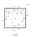
- Figure 5A is a schematic top view of a tester 500 for performing diode measurements
- Figure 5B is a schematic cross-sectional view of the tester 500 along line 5-5 of Figure 5A
- Tester 500 may comprise a substrate 502 with thin films formed thereover and separated into isolation regions 510, inner probe regions 520, outer probe regions 521, inner active region 530, and outer active region 531.
- a front TCO layer 505 may be formed over the substrate 502.
- one or more insulating grooves 512 may be created for interrupting lateral current in the TCO layer 505 and configured within each isolation region 510.
- an insulating groove 513 may be created for interrupting lateral current in the TCO layer 505 and configured through the inner active region 530 and the outer active region 531.
- an absorber layer 515 may be formed over the TCO layer 505.
- one or more grooves 526 are created in layer 515, within the outer active region 531.
- a back reflective layer 525 may be formed over the absorber layer 515, such that an electrical connection is formed between the TCO layer 505 and the back reflective layer 525 through one or more grooves 526.
- one or more insulating grooves 516 may be created in the back reflective layer 525 within each isolation region 510 to electrically isolate the tester 500 from adjacent devices. Additionally, one or more insulating grooves 536 may be created in the back reflective layer 525 to electrically interrupt lateral current in the back reflective layer 525 between the inner active region 530 and the outer active region 531. The one or more insulating grooves 536 also interrupt lateral current between the inner probe regions 520 and the outer probe regions 521 as well as interrupting current between the inner active region 530 and the outer probe regions 521.
- tester 500 may have four probing regions for performing four-terminal measurements. Two terminals may connect to the back reflective layer 525 in the outer probe regions 521 to electrically connect to the TCO layer 505 via the one or more grooves 526 in the outer active region 531. The other two terminals may connect to the back reflective layer 525 in the inner probe regions 520, which is laterally, electrically insulated from the back reflective layer 525 outer probe regions 521 and the outer active region 531.
- a number of measurements may be taken, including but not limited to, dark saturation current, ideality factor, and series resistance. Additionally, with the proper light source, solar cell parameters such as short-circuit current, open-circuit voltage, and fill-factor may be determined.
- testers of the present invention a plurality of testers may be produced onto a single substrate.
- the testers may be defined using computer-aided design software, allowing continuous modification as information is required for process development and yield improvement. For example, if a contact resistance problem is suspected in a particular production run of solar cells, a suite of chain testers may be processed between solar cell production runs. Similarly, if a uniformity problem exists, an array of cells may be fabricated and measured to obtain mapping data. Additionally, in fabrication line ramp-up and line diagnostic settings, a standard set of testers may be fabricated in a fabrication line at a remote location. The testers may then be sent back to a central facility or measured on site. The data may then be compared to data obtained from a reference process. Thus, embodiments of the present invention allow continuous, in-line testing of parameters directly related to the process.
- Figure 6 is a schematic top view of an exemplary embodiment of groups of testers 200, 300, 400, and 500 produced on a single substrate 602.
- a possible configuration of contact resistance testers 200, metallic layer sheet resistance testers 300, TCO layer sheet resistance testers 400, and diode testers 500 may be grouped and produced on a single substrate 602.
- a plurality of contact testers 200 may be grouped and produced on a single substrate.
- testers of the present invention may be grouped and sized for maximum space utilization in any number of combinations.
- FIG. 7 is a schematic top view of four PV modules 100 formed atop a single substrate 702.
- testers 700 which may be tester 200, 300, 400, 500, a combination thereof or another tester, may be formed in the cut area 705 between modules 100.
- the substrate 702 is cut into modules 100, wherein the cut area 705 is destroyed.
- Figure 7 shows four modules 100 cut from a single substrate; however, any number of modules 100 may be cut from a single substrate.
- testers 700 may be placed in a periphery area, which is also destroyed, or testers 700 may be substituted for one or more of the modules 100.
- testers 700 may be formed during normal production runs of PV modules 100 in configurations that make best use of the available space.
- Further embodiments of the present invention comprise methods for determining process design rules for producing PV cells, testers or modules for optimum performance, production yield and efficiency.
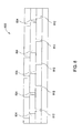
- An embodiment of the present invention comprises methods for determining process design rules associated with spacing of laser scribed grooves in a PV cell, tester or module. For example, to determine the spacing between insulating groove 112 and groove 124 in the PV module of Figure 1 , a series of testers with varying spacing may be fabricated. Importantly, the methodology of varying the spacing may be performed automatically via software programming or manually input into the laser scribing system.
- Figure 8 is a schematic cross-sectional view of an embodiment of the present invention 800 comprising a test module having a series of cells with varied spacing between insulating groove 812 and groove 824.
Landscapes
- Photovoltaic Devices (AREA)
- Testing Of Individual Semiconductor Devices (AREA)
- Testing Or Measuring Of Semiconductors Or The Like (AREA)
Abstract
The present invention generally relates to process testers and methods of fabricating the same using standard photovoltaic cell processes. In particular, the present invention relates to process tester layouts defined by laser scribing, methodology for creating process testers, methodology of using process testers for photovoltaic line diagnostics, placement of process testers in photovoltaic module production, and methodology for creating design rule testers.
Description
- Embodiments of the present invention generally relate to photovoltaic devices and fabrication processes thereof. In particular, embodiments of the present invention relate to process testers, methods of manufacturing process testers, and testing methodology for thin-film photovoltaic devices.
- Photovoltaic (PV) devices are devices that convert sunlight into direct current (DC) electrical power. A PV device may be classified as monocrystalline, polycrystalline, or thin-film depending on how the device is fabricated.
- Monocrystalline PV devices are produced by slicing wafers from a single crystal, high purity, silicon boule. Polycrystalline PV devices are produced by sawing a cast block of silicon into bars, then wafers. Thin-film PV devices are produced by depositing thin layers of materials, such as amorphous silicon, microcrystalline silicon or copper indium gallium selenide (CIGS), onto a suitable substrate.
- Although monocrystalline and polycrystalline silicon have traditionally produced PV devices with higher efficiencies, the high cost of crystalline silicon wafers has led the industry into increased use and development of thin-film PV devices.
- Accordingly, as the production of thin-film PV devices matures, the need for increased process control has developed. This need is driven by both yield and uniformity considerations. Additionally, fast and effective solving of ramp-up problems associated with new or duplicated production lines is needed as well.
- Therefore, a need exists for process testers and testing methodology for thin-film PV devices that can provide, through electrical testing, information directly related to the production process.
- In light of the above, a method for forming a device for testing thin-film, photovoltaic production processes according to
independent claims 1 and 5, a method for producing devices for testing thin-film, photovoltaic production processes according to independent claims 11 and 12, a method for determining thin-film, photovoltaic cell, tester or module process design rules according to independent claim 13, and a device for testing thin-film, photovoltaic production processes according to independent claims 6 and 10 are provided. - The present invention generally provides process tester layouts defined by laser scribing, methodology for creating process testers, methodology of using process testers for solar line diagnostics, placement of process testers in PV module production, and methodology for creating design rule testers.
- In one embodiment of the present invention, a method for forming a device for testing thin-film, photovoltaic production processes comprises forming a front transparent conductive oxide layer over a substrate, laser scribing a groove in the front transparent conductive oxide layer in an isolation region of the device, forming an absorber layer over the front transparent conductive oxide layer, laser scribing a groove in the absorber layer in a first probe region of the device, laser scribing a groove in the absorber layer in a second probe region of the device, forming a back reflective layer over the absorber layer, laser scribing a groove in the back reflective layer in the isolation region of the device, and laser scribing a groove in the back reflective layer in a linking region of the device. In one embodiment, the isolation region electrically isolates the device from adjacent photovoltaic structures.
- In another embodiment, a method for forming a device for testing thin-film, photovoltaic production processes comprises forming a front transparent conductive oxide layer over a substrate, laser scribing a groove in the front transparent conductive oxide layer in an isolation region of the device, laser scribing a groove in the transparent conductive oxide layer across an outer and inner active region of the device, forming an absorber layer over the front transparent conductive oxide layer, laser scribing a groove in the absorber layer in the outer active region of the device prior, forming a back reflective layer over the absorber layer, laser scribing a groove in the back reflective layer in the isolation region of the device, and laser scribing a groove in the back reflective layer between the outer active region and the inner active region of the device. In one embodiment, the isolation region electrically isolates the device from adjacent photovoltaic structures.
- In another embodiment, a device for testing thin-film, photovoltaic production processes comprises a front transparent conductive oxide layer formed over a substrate, an absorber layer formed over the front transparent conductive oxide layer, and a back reflective layer formed over the absorber layer. In one embodiment, the transparent conductive oxide layer has a groove in an isolation region of the device. In one embodiment, the absorber layer has a groove in a first probe region of the device and a groove in a second probe region of the device. In one embodiment, the back reflective layer has a groove in the isolation region of the device. In one embodiment, the isolation region electrically isolates the device from adjacent photovoltaic structures. In one embodiment, wherein the back reflective layer has a groove in a linking region of the device.
- In another embodiment, a device for testing thin-film, photovoltaic production processes comprises a front transparent conductive oxide layer formed over a substrate, an absorber layer formed over the front transparent conductive oxide layer, and a back reflective layer formed over the absorber layer, wherein. In one embodiment, the transparent conductive oxide layer has a groove in an isolation region of the device and a groove across an outer and inner active region of the device. In one embodiment, the absorber layer has a groove in the outer active region of the device. In one embodiment, the back reflective layer has a groove in the isolation region of the device, the isolation region electrically isolates the device from adjacent photovoltaic structures, and the back reflective layer has a groove between the outer active region and the inner active region of the device.
- In another embodiment, a method for producing devices for testing thin-film, photovoltaic production processes comprises forming a plurality of devices on a single substrate, wherein the devices are defined via laser scribing, wherein the plurality of devices is selected from the group consisting of a tester for measuring the contact resistance between a front transparent conductive oxide layer and a back reflective layer, a tester for measuring the back reflective layer sheet resistance, a tester for measuring the front transparent conductive oxide layer sheet resistance, and a tester for measuring diode characteristics, and wherein the location, position, and number of devices are manipulated and controlled during the production of photovoltaic modules.
- In another embodiment, a method for producing devices for testing thin-film, photovoltaic production processes comprises forming a photovoltaic module on a substrate and forming a photovoltaic process tester on the substrate, wherein the tester is defined via laser scribing, wherein the tester is selected from the group consisting of a tester for measuring the contact resistance between a front transparent conductive oxide layer and a back reflective layer, a tester for measuring the back reflective layer sheet resistance, a tester for measuring the front transparent conductive oxide layer sheet resistance, and a tester for measuring diode characteristics, and wherein the tester is located in a cut area of the substrate.
- In yet another embodiment of the present invention, a method for determining thin-film, photovoltaic cell, tester or module process design rules comprises forming a plurality of photovoltaic cells and laser scribing grooves in each layer of the cells, wherein lateral distances between the grooves are varied to determine spacing for desired process characteristics. In one embodiment, the photovoltaic cells comprise a transparent conductive oxide layer formed over a substrate, an absorber layer formed over the transparent conductive oxide layer, and a back reflective layer formed over the absorber layer.
- Further advantages, features, aspects and details that can be combined with embodiments described herein are evident from the dependent claims, the description and the drawings.
- The invention is also directed to a device for carrying out the disclosed methods and including device parts for performing each described method steps. Furthermore, the invention is also directed to methods by which the described device operates. It includes method steps for carrying out every function of the device.
- So that the manner in which the above recited features of the present invention can be understood in detail, a more particular description of the invention, briefly summarized above, may be had by reference to embodiments, some of which are illustrated in the appended drawings. It is to be noted, however, that the appended drawings illustrate only typical embodiments of this invention and are therefore not to be considered limiting of its scope, for the invention may admit to other equally effective embodiments.
-
Figure 1 is a schematic cross-section of a thin-film PV module showing series connections between individual cells. -
Figure 2 is a schematic cross-sectional view of an embodiment of a tester for measuring the contact resistance between a TCO layer and a back reflective layer. -
Figure 3 is a schematic cross-sectional view of an embodiment of a tester for measuring the sheet resistance in a back reflective layer. -
Figure 4 is a schematic cross-sectional view of an embodiment of a tester for measuring sheet resistance of a front TCO layer. -
Figure 5A is a schematic top view of a tester for performing diode measurements. -
Figure 5B is a schematic cross-sectional view of the tester inFigure 5A along line 5-5. -
Figure 6 is a schematic top view of an exemplary embodiment of groups of testers produced on a single substrate. -
Figure 7 is a schematic top view of four solar modules formed atop a single substrate. -
Figure 8 is a schematic cross-sectional view of an embodiment of the present invention comprising a test module having a series of cells with varied lateral spacing between insulating transparent conductive oxide layer grooves and absorber layer grooves. - The present invention generally comprises process testers fabricated using standard PV device processes or standard photovoltaic cell processes. In particular, the present invention comprises process tester layouts defined by laser scribing, methodology for creating process testers, methodology of using process testers for solar line diagnostics, photovoltaic line diagnostics, placement of process testers in PV module production, and methodology for creating design rule testers.
- In thin-film PV module fabrication, individual PV cells may be formed and interconnected into a module via laser scribing the layers of the cell.
Figure 1 is a schematic cross-section of a thin-film PV module 100 showing series connections betweenindividual cells 101.PV module 100 comprises asubstrate 102, such as a glass or polymer substrate, with thin films formed thereover. - In the
PV module 100 fabrication process, a front transparent conducting oxide (TCO)layer 105 may be formed over thesubstrate 102. TheTCO layer 105 may comprise tin oxide, zinc oxide, indium tin oxide, cadmium stannate, combinations thereof, or other suitable materials. In a first laser scribing step, a firstinsulating groove 112 may be created in theTCO layer 105 to interrupt lateral current flow. Anabsorber layer 115 may then be formed over theTCO layer 105. Theabsorber layer 115 may comprise layers of thin films, including but not limited to, amorphous silicon, microcrystalline silicon, copper indium gallium selenide (CIGS), or combinations thereof. Next, a second laser scribing may create agroove 124 in theabsorber layer 115, which may be filled during the subsequent step of forming a backreflective layer 125 over theabsorber layer 115. This results in an interconnection between thefront TCO layer 105 and the backreflective layer 125. The backreflective layer 125 may comprise a conductive layer and/or a reflective coating. The conductive layer may be a second TCO layer. The reflective coating may comprise metallic materials including, but not limited to Al, Ag, Ti, Cr, Au, Cu, Pt, alloys thereof, combinations thereof as well as other conductive and reflective materials. Finally, a secondinsulating groove 136 may be formed in the backreflective layer 125 to interrupt lateral current flow in the backreflective layer 125. - As a result, each
individual PV cell 101 ofmodule 100 is electrically connected in series with eachadjacent cell 101.Figure 1 depicts fivePV cells 101 connected in series via the aforementioned laser scribing process; however, any number ofPV cells 101 may be linked in this manner to formPV module 100. - In thin-film PV fabrication, such devices are manufactured on production lines on a large scale. End of line testing may provide finished product information, such as module electrical characteristics, but it does not provide direct information as to the root causes of process failures. Embodiments of the present invention provide testers that may be produced before, during, or after process runs to provide direct information, such as sheet and contact resistance of the conducting layers and the saturation current density of the diode component of the device, needed to diagnose root causes of process failures.
- Embodiments of the present invention involve creating process testers by means of the same laser scribing processes used for creating and interconnecting
PV cells 101 withinPV module 100. -
Figure 2 is a schematic cross-sectional view of an embodiment of atester 200 for measuring the contact resistance between a TCO layer and a back reflective layer. Thetester 200 comprises asubstrate 202 with thin films formed thereover and divided intoisolation regions 210,probe regions 220, and one or more linkingregions 230. - In fabricating the
tester 200, afront TCO layer 205 may be formed over thesubstrate 202. In a first laser scribing,TCO insulating grooves TCO layer 205, such that one ormore grooves 212 are configured within eachisolation region 210, one ormore grooves 222 are configured within eachprobe region 220, and one ormore grooves 232 are configured within each linkingregion 230. Thus, the lateral current inTCO layer 205 is interrupted by insulatinggrooves - Next, an
absorber layer 215 may be formed over theTCO layer 205. In a second laser scribing,grooves absorber layer 215, such that one ormore grooves 224 are configured within eachprobe region 220 and one ormore grooves 234 are configured within each linkingregion 230. Although one or more grooves may be created in eachisolation region 210 of theabsorber layer 215, this is generally not necessary due to the low lateral conductivity of theabsorber layer 215. - Subsequently, a back
reflective layer 225 may be formed over theabsorber layer 215, such that electrical interconnection is established between the backreflective layer 225 and theTCO layer 205 atgrooves layer insulating grooves reflective layer 225, such that one ormore grooves 216 are configured within eachisolation region 210 and one ormore grooves 236 are configured within each linkingregion 230. Thus, lateral current in backreflective layer 225 is interrupted by insulatinggrooves - As shown in
Figure 2 , the resultingtester 200 comprisesisolation regions 210,probe regions 220, and one or more linkingregions 230. Theisolation regions 210 electrically isolate thetester 200 from adjacent structures. An electrically interconnected chain is established between theprobe regions 220 through the one or more linkingregions 230, wherein conduction alternates between the backreflective layer 225 and theTCO layer 205. AlthoughFigure 2 depicts onelinking region 230, any number of linkingregions 230 may be interconnected in thetester 200. - In using the
tester 200 for testing the contact resistance between the backreflective layer 225 and theTCO layer 205, electrical probes, such as commonly used in automated testing facilities, may be placed in contact with the backreflective layer 225, within eachprobe region 220 of thetester 200. The resistance measured between the two probes is dominated by the contact between the backreflective layer 225 and theTCO layer 205. Therefore, the contact resistance is approximately equal to the measured resistance divided by the sum of the number ofgrooves -
Figure 3 is a schematic cross-sectional view of an embodiment of atester 300 for measuring the sheet resistance in a back reflective layer. Thetester 300 comprises asubstrate 302 having thin films formed thereover and divided intoisolation regions 310,probe regions 320, and alinking region 330. - In fabricating the
tester 300, afront TCO layer 305 may be formed over thesubstrate 302. In a first laser scribing, aTCO insulating groove 312 may be created in theTCO layer 305, such that one ormore grooves 312 are configured within eachisolation region 310. Thus, the current in theTCO layer 305 is interrupted bygrooves 312. - Next, an
absorber layer 315 may be formed over theTCO layer 305. Subsequently, a backreflective layer 325 may be formed over theabsorber layer 315. - In a second laser scribing process, one or more
insulating grooves 316 may be created within eachisolation region 310 to electrically isolate the backmetal resistance tester 300 from adjacent structures. - In operation, an electrical probe may be placed in contact with the back
reflective layer 325 in eachprobe region 320, and the resistance between the probes may be measured. Since no electrical interconnection exists between the backreflective layer 325 and theTCO layer 305, the resistance measured between the probes is approximately equivalent to the sheet resistance in the backreflective layer 325. -
Figure 4 is a schematic cross-sectional view of an embodiment of atester 400 for measuring sheet resistance of a front TCO layer.Tester 400 comprises asubstrate 402 with thin films formed thereover and divided intoisolation regions 410,probe regions 420, and alinking region 430. - In fabricating a
tester 400, afront TCO layer 405 may be formed over thesubstrate 402. In a first laser scribing, aTCO insulating groove 412 may be created in theTCO layer 405, such that one ormore grooves 412 are configured within eachisolation region 410. Thus, the current in theTCO layer 405 is interrupted bygrooves 412. - An
absorber layer 415 may then be formed over theTCO layer 405. In a second laser scribing process, one ormore grooves 424 may be created inabsorber layer 415 and configured within eachprobe region 420. - Subsequently, a back
reflective layer 425 may be formed overabsorber layer 415, such that an electrical connection is formed between backreflective layer 425 andTCO layer 405 atgrooves 424. - In a third laser scribing process, one or more
insulating grooves 416 may be created within eachisolation region 410 to electrically isolate thetester 400 from adjacent structures. Additionally, one or moreinsulating grooves 436 may be created within thelinking region 430 oftester 400 to interrupt lateral current in the backreflective layer 425. - In operation, an electrical probe may be placed in contact with the back
reflective layer 425 in eachprobe region 420, and the resistance between the probes may be measured. Since the lateral current in the backreflective layer 425 is interrupted via one or moreinsulating grooves 436, the lateral conduction is dominated by theTCO layer 405. Therefore, the resistance measured between the probes is approximately equivalent to the sheet resistance of theTCO layer 405. -
Figure 5A is a schematic top view of atester 500 for performing diode measurements, andFigure 5B is a schematic cross-sectional view of thetester 500 along line 5-5 ofFigure 5A .Tester 500 may comprise asubstrate 502 with thin films formed thereover and separated intoisolation regions 510,inner probe regions 520,outer probe regions 521, inneractive region 530, and outeractive region 531. - In fabricating the
tester 500, afront TCO layer 505 may be formed over thesubstrate 502. In a first laser scribing, one or moreinsulating grooves 512 may be created for interrupting lateral current in theTCO layer 505 and configured within eachisolation region 510. Additionally, an insulatinggroove 513 may be created for interrupting lateral current in theTCO layer 505 and configured through the inneractive region 530 and the outeractive region 531. - Next, an
absorber layer 515 may be formed over theTCO layer 505. In a second laser scribing process, one ormore grooves 526 are created inlayer 515, within the outeractive region 531. - Subsequently, a back
reflective layer 525 may be formed over theabsorber layer 515, such that an electrical connection is formed between theTCO layer 505 and the backreflective layer 525 through one ormore grooves 526. - In a third laser scribing process, one or more
insulating grooves 516 may be created in the backreflective layer 525 within eachisolation region 510 to electrically isolate thetester 500 from adjacent devices. Additionally, one or moreinsulating grooves 536 may be created in the backreflective layer 525 to electrically interrupt lateral current in the backreflective layer 525 between the inneractive region 530 and the outeractive region 531. The one or moreinsulating grooves 536 also interrupt lateral current between theinner probe regions 520 and theouter probe regions 521 as well as interrupting current between the inneractive region 530 and theouter probe regions 521. - In one embodiment,
tester 500 may have four probing regions for performing four-terminal measurements. Two terminals may connect to the backreflective layer 525 in theouter probe regions 521 to electrically connect to theTCO layer 505 via the one ormore grooves 526 in the outeractive region 531. The other two terminals may connect to the backreflective layer 525 in theinner probe regions 520, which is laterally, electrically insulated from the backreflective layer 525outer probe regions 521 and the outeractive region 531. As a result of the configuration oftester 500, a number of measurements may be taken, including but not limited to, dark saturation current, ideality factor, and series resistance. Additionally, with the proper light source, solar cell parameters such as short-circuit current, open-circuit voltage, and fill-factor may be determined. - In fabricating testers of the present invention, a plurality of testers may be produced onto a single substrate. The testers may be defined using computer-aided design software, allowing continuous modification as information is required for process development and yield improvement. For example, if a contact resistance problem is suspected in a particular production run of solar cells, a suite of chain testers may be processed between solar cell production runs. Similarly, if a uniformity problem exists, an array of cells may be fabricated and measured to obtain mapping data. Additionally, in fabrication line ramp-up and line diagnostic settings, a standard set of testers may be fabricated in a fabrication line at a remote location. The testers may then be sent back to a central facility or measured on site. The data may then be compared to data obtained from a reference process. Thus, embodiments of the present invention allow continuous, in-line testing of parameters directly related to the process.
-
Figure 6 is a schematic top view of an exemplary embodiment of groups oftesters single substrate 602. InFigure 6 , a possible configuration ofcontact resistance testers 200, metallic layersheet resistance testers 300, TCO layersheet resistance testers 400, anddiode testers 500 may be grouped and produced on asingle substrate 602. - Any number of configurations of groups of testers is possible and is intended within the scope of the invention. For example, a plurality of
contact testers 200 may be grouped and produced on a single substrate. Further, testers of the present invention may be grouped and sized for maximum space utilization in any number of combinations. - Additionally, process testers according to the present invention may be produced along with solar modules on a single substrate.
Figure 7 is a schematic top view of fourPV modules 100 formed atop asingle substrate 702. During the same production run,testers 700, which may betester cut area 705 betweenmodules 100. After production and testing, thesubstrate 702 is cut intomodules 100, wherein thecut area 705 is destroyed.Figure 7 shows fourmodules 100 cut from a single substrate; however, any number ofmodules 100 may be cut from a single substrate. Optionally,testers 700 may be placed in a periphery area, which is also destroyed, ortesters 700 may be substituted for one or more of themodules 100. Thus,testers 700 may be formed during normal production runs ofPV modules 100 in configurations that make best use of the available space. - Further embodiments of the present invention comprise methods for determining process design rules for producing PV cells, testers or modules for optimum performance, production yield and efficiency.
- An embodiment of the present invention comprises methods for determining process design rules associated with spacing of laser scribed grooves in a PV cell, tester or module. For example, to determine the spacing between insulating
groove 112 and groove 124 in the PV module ofFigure 1 , a series of testers with varying spacing may be fabricated. Importantly, the methodology of varying the spacing may be performed automatically via software programming or manually input into the laser scribing system. -
Figure 8 is a schematic cross-sectional view of an embodiment of thepresent invention 800 comprising a test module having a series of cells with varied spacing between insulatinggroove 812 andgroove 824. - While the foregoing is directed to embodiments of the present invention, other and further embodiments of the invention may be devised without departing from the basic scope thereof, and the scope thereof is determined by the claims that follow.
Claims (15)
- A method for forming a device for testing thin-film, photovoltaic production processes, comprising:forming a front transparent conductive oxide layer (205, 305, 405) over a substrate (202, 302, 402);laser scribing a groove (212, 312, 412) in the front transparent conductive oxide layer in an isolation region (210, 310, 410) of the device;forming an absorber layer (215, 315, 415) over the front transparent conductive oxide layer;laser scribing a groove (224, 424) in the absorber layer in a first probe region (220, 320, 420) of the device;laser scribing a groove (224, 424) in the absorber layer in a second probe region (220, 320, 420) of the device;forming a back reflective layer (225, 325, 425) over the absorber layer;laser scribing a groove (216, 316, 416) in the back reflective layer in the isolation region of the device, wherein the isolation region electrically isolates the device from adjacent photovoltaic structures; andlaser scribing a groove (236, 436) in the back reflective layer in a linking region (230, 430) of the device.
- The method of claim 1, further comprising laser scribing a groove (222) in the front transparent conductive oxide layer in the first probe region and a groove (222) in the front transparent conductive oxide layer in the second probe region prior to forming the absorber layer.
- The method of any of the claims 1 to 2, further comprising laser scribing a groove (232) in the front transparent conductive oxide layer in the linking region prior to forming the absorber layer.
- The method of any of the claims 1 to 3, further comprising laser scribing a groove (234) in the absorber layer in the linking region prior to forming the back reflective layer.
- A method for forming a device for testing thin-film, photovoltaic production processes, comprising:forming a front transparent conductive oxide layer (505) over a substrate (502);laser scribing a groove (512) in the front transparent conductive oxide layer in an isolation region (510) of the device;laser scribing a groove (513) in the transparent conductive oxide layer across an outer active region (531) and an inner active region (530) of the device;forming an absorber layer (515) over the front transparent conductive oxide layer;laser scribing a groove (526) in the absorber layer in the outer active region of the device;forming a back reflective layer (525) over the absorber layer;laser scribing a groove (516) in the back reflective layer in the isolation region of the device, wherein the isolation region electrically isolates the device from adjacent photovoltaic structures; andlaser scribing a groove (536) in the back reflective layer between the outer active region and the inner active region of the device.
- A device for testing thin-film, photovoltaic production processes, comprising:a front transparent conductive oxide layer (205, 305, 405) formed over a substrate (202, 302, 402), wherein the transparent conductive oxide layer has a groove (212, 312, 412) in an isolation region (210, 310, 410) of the device;an absorber layer (215, 315, 415) formed over the front transparent conductive oxide layer, wherein the absorber layer has a groove (224, 424) in a first probe region (220, 320, 420) of the device and a groove (224, 424) in a second probe region (220, 320, 420) of the device; anda back reflective layer (225, 325, 425) formed over the absorber layer, wherein the back reflective layer has a groove (216, 316, 416) in the isolation region of the device, wherein the isolation region electrically isolates the device from adjacent photovoltaic structures, and wherein the back reflective layer has a groove (236, 436) in a linking region (230, 430) of the device.
- The device of claim 6, wherein the transparent conductive oxide layer has a groove (222) in the first probe region and a groove (222) in the second probe region.
- The device of any of the claims 6 to 7, wherein the transparent conductive oxide layer has a groove (232) in the linking region.
- The method of any of the claims 6 to 8, wherein the absorber layer has a groove (234) in the linking region.
- A device for testing thin-film, photovoltaic production processes, comprising:a front transparent conductive oxide layer (505) formed over a substrate (502), wherein the transparent conductive oxide layer has a groove (512) in an isolation region (510) of the device, and wherein the front transparent conductive oxide layer has a groove (513) across an outer active region (531) and an inner active region (530) of the device;an absorber layer (515) formed over the front transparent conductive oxide layer, wherein the absorber layer has a groove (526) in the outer active region of the device; anda back reflective layer (525) formed over the absorber layer, wherein the back reflective layer has a groove (516) in the isolation region of the device, wherein the isolation region electrically isolates the device from adjacent photovoltaic structures, and wherein the back reflective layer has a groove (536) between the outer active region and the inner active region of the device.
- A method for producing devices for testing thin-film, photovoltaic production processes, comprising forming a plurality of devices on a single substrate (602), wherein the devices are defined via laser scribing, wherein the plurality of devices is selected from the group consisting of a tester (200) for measuring the contact resistance between a front transparent conductive oxide layer and a back reflective layer, a tester (300) for measuring the back reflective layer sheet resistance, a tester (400) for measuring the front transparent conductive oxide layer sheet resistance, and a tester (500) for measuring diode characteristics, and wherein the location, position, and number of devices are manipulated and controlled during the production of photovoltaic modules.
- A method for producing devices for testing thin-film, photovoltaic production processes, comprising:forming a photovoltaic module (100) on a substrate (702); andforming a photovoltaic process tester (700) on the substrate, wherein the tester is defined via laser scribing, wherein the tester is selected from the group consisting of a tester (200) for measuring the contact resistance between a front transparent conductive oxide layer and a back reflective layer, a tester (300) for measuring the back reflective layer sheet resistance, a tester (400) for measuring the front transparent conductive oxide layer sheet resistance, and a tester (500) for measuring diode characteristics, and wherein the tester is located in a cut area (705) of the substrate.
- A method for determining thin-film, photovoltaic cell, tester or module process design rules, comprising:forming a plurality of photovoltaic cells, wherein the photovoltaic cells comprise:a transparent conductive oxide layer (205, 305, 405, 505) formed over a substrate (202, 302, 402, 502, 602, 702);an absorber layer (215, 315, 415, 515) formed over the transparent conductive oxide layer; anda back reflective layer (225, 325, 425, 525) formed over the absorber layer; andlaser scribing grooves (212, 216, 222, 224, 232, 234, 236, 312, 316, 412, 416, 424, 436, 512, 513, 516, 526, 536, 812, 824) in each layer of the cells, wherein lateral distances between the grooves are varied to determine spacing for desired process characteristics.
- The method of claim 13, wherein lateral distances between the grooves in the transparent conductive oxide layer and grooves in the absorber layer are varied to determine spacing for desired process characteristics.
- The method of any of the claims 13 to 14, wherein the lateral distances between grooves in the absorber layer and grooves in the back reflective layer are varied to determine spacing for desired process characteristics.
Applications Claiming Priority (1)
| Application Number | Priority Date | Filing Date | Title |
|---|---|---|---|
| US11/876,346 US20090102502A1 (en) | 2007-10-22 | 2007-10-22 | Process testers and testing methodology for thin-film photovoltaic devices |
Publications (1)
| Publication Number | Publication Date |
|---|---|
| EP2053665A2 true EP2053665A2 (en) | 2009-04-29 |
Family
ID=40347927
Family Applications (1)
| Application Number | Title | Priority Date | Filing Date |
|---|---|---|---|
| EP08167335A Withdrawn EP2053665A2 (en) | 2007-10-22 | 2008-10-22 | Process testers and testing methodology for thin-film photovoltaic devices |
Country Status (7)
| Country | Link |
|---|---|
| US (1) | US20090102502A1 (en) |
| EP (1) | EP2053665A2 (en) |
| JP (1) | JP2009105401A (en) |
| KR (1) | KR20090040846A (en) |
| CN (2) | CN101494250A (en) |
| TW (1) | TW200929413A (en) |
| WO (1) | WO2009055208A1 (en) |
Cited By (2)
| Publication number | Priority date | Publication date | Assignee | Title |
|---|---|---|---|---|
| CN102983785A (en) * | 2011-09-02 | 2013-03-20 | 杜邦太阳能有限公司 | Photoelectric conversion system |
| WO2023027299A1 (en) * | 2021-08-25 | 2023-03-02 | 한밭대학교 산학협력단 | Lateral photocurrent method for directly measuring sheet resistance of cds in cu(in, ga)se2 element under element operation condition |
Families Citing this family (13)
| Publication number | Priority date | Publication date | Assignee | Title |
|---|---|---|---|---|
| US7829356B2 (en) * | 2008-09-17 | 2010-11-09 | Applied Materials, Inc. | Thin film scribe process |
| DE102009021273A1 (en) * | 2009-05-14 | 2010-11-18 | Schott Solar Ag | Method and device for producing a photovoltaic thin-film module |
| WO2011006050A1 (en) * | 2009-07-10 | 2011-01-13 | First Solar, Inc. | Photovoltaic devices including zinc |
| JP5702387B2 (en) | 2009-09-21 | 2015-04-15 | アップル インコーポレイテッド | Signaling and channel estimation for uplink transmit diversity |
| CN101900785A (en) * | 2009-09-28 | 2010-12-01 | 新奥光伏能源有限公司 | Method for measuring surface resistance and contact resistance of solar battery and measuring tool thereof |
| CN102082198B (en) * | 2010-09-30 | 2012-11-21 | 深圳市创益科技发展有限公司 | High-power low-voltage silicon-based thin film solar cell and manufacturing method thereof |
| CN102610691A (en) * | 2010-10-12 | 2012-07-25 | 上方能源技术(杭州)有限公司 | Method for manufacturing thin-film solar battery module and apparatus thereof |
| JP2013247165A (en) * | 2012-05-23 | 2013-12-09 | Mitsubishi Electric Corp | Thin-film solar battery module and manufacturing method therefor |
| DE102012104844B4 (en) | 2012-06-05 | 2017-06-29 | Heliatek Gmbh | Optical system and method for monitoring and controlling photoactive components in the production process |
| CN103456842B (en) * | 2013-09-13 | 2016-03-16 | 英利集团有限公司 | Preparation technology's method of testing of N-type solar cell selective back surface field |
| CN103489964A (en) * | 2013-10-15 | 2014-01-01 | 山东禹城汉能光伏有限公司 | Manufacturing method of BIPV (Building Integrated Photovoltaics) thin-film solar cell |
| CN108183144B (en) * | 2017-12-27 | 2020-10-16 | 四川大学 | A laser scribing technique to improve the testing accuracy of cadmium telluride thin-film solar cells |
| IT201800006167A1 (en) | 2018-06-08 | 2019-12-08 | EQUIPMENT FOR LASER ENGRAVING OF INSOLES AND METHOD OF OPERATION OF THIS EQUIPMENT |
Family Cites Families (14)
| Publication number | Priority date | Publication date | Assignee | Title |
|---|---|---|---|---|
| US4144493A (en) * | 1976-06-30 | 1979-03-13 | International Business Machines Corporation | Integrated circuit test structure |
| JPS5961077A (en) * | 1982-09-29 | 1984-04-07 | Nippon Denso Co Ltd | Amorphous silicon solar battery |
| US4443652A (en) * | 1982-11-09 | 1984-04-17 | Energy Conversion Devices, Inc. | Electrically interconnected large area photovoltaic cells and method of producing said cells |
| US4628144A (en) * | 1983-06-07 | 1986-12-09 | California Institute Of Technology | Method for contact resistivity measurements on photovoltaic cells and cell adapted for such measurement |
| US4667058A (en) * | 1985-07-01 | 1987-05-19 | Solarex Corporation | Method of fabricating electrically isolated photovoltaic modules arrayed on a substrate and product obtained thereby |
| US4892592A (en) * | 1987-03-26 | 1990-01-09 | Solarex Corporation | Thin film semiconductor solar cell array and method of making |
| JP3510740B2 (en) * | 1996-08-26 | 2004-03-29 | シャープ株式会社 | Manufacturing method of integrated thin-film solar cell |
| JP2000059986A (en) * | 1998-04-08 | 2000-02-25 | Canon Inc | Solar cell module failure detection method and apparatus, and solar cell module |
| US6468828B1 (en) * | 1998-07-14 | 2002-10-22 | Sky Solar L.L.C. | Method of manufacturing lightweight, high efficiency photovoltaic module |
| US6077722A (en) * | 1998-07-14 | 2000-06-20 | Bp Solarex | Producing thin film photovoltaic modules with high integrity interconnects and dual layer contacts |
| US6281696B1 (en) * | 1998-08-24 | 2001-08-28 | Xilinx, Inc. | Method and test circuit for developing integrated circuit fabrication processes |
| EP1253644A1 (en) * | 2001-04-23 | 2002-10-30 | Diego Dr. Fischer | Electric power generating device and method of fabrication |
| US7259321B2 (en) * | 2002-01-07 | 2007-08-21 | Bp Corporation North America Inc. | Method of manufacturing thin film photovoltaic modules |
| US8084400B2 (en) * | 2005-10-11 | 2011-12-27 | Intermolecular, Inc. | Methods for discretized processing and process sequence integration of regions of a substrate |
-
2007
- 2007-10-22 US US11/876,346 patent/US20090102502A1/en not_active Abandoned
-
2008
- 2008-09-29 WO PCT/US2008/078165 patent/WO2009055208A1/en not_active Ceased
- 2008-10-15 KR KR1020080101081A patent/KR20090040846A/en not_active Ceased
- 2008-10-20 JP JP2008270178A patent/JP2009105401A/en not_active Withdrawn
- 2008-10-22 CN CNA200810171158XA patent/CN101494250A/en active Pending
- 2008-10-22 EP EP08167335A patent/EP2053665A2/en not_active Withdrawn
- 2008-10-22 CN CNA2008101734030A patent/CN101425550A/en active Pending
- 2008-10-22 TW TW097140528A patent/TW200929413A/en unknown
Cited By (3)
| Publication number | Priority date | Publication date | Assignee | Title |
|---|---|---|---|---|
| CN102983785A (en) * | 2011-09-02 | 2013-03-20 | 杜邦太阳能有限公司 | Photoelectric conversion system |
| WO2023027299A1 (en) * | 2021-08-25 | 2023-03-02 | 한밭대학교 산학협력단 | Lateral photocurrent method for directly measuring sheet resistance of cds in cu(in, ga)se2 element under element operation condition |
| KR20230030330A (en) * | 2021-08-25 | 2023-03-06 | 한밭대학교 산학협력단 | Lateral photocurrent method for directly measuring the sheet resistance of cds on cu(in, ga)se2 devices under device operating conditions |
Also Published As
| Publication number | Publication date |
|---|---|
| WO2009055208A1 (en) | 2009-04-30 |
| CN101494250A (en) | 2009-07-29 |
| TW200929413A (en) | 2009-07-01 |
| CN101425550A (en) | 2009-05-06 |
| US20090102502A1 (en) | 2009-04-23 |
| KR20090040846A (en) | 2009-04-27 |
| JP2009105401A (en) | 2009-05-14 |
Similar Documents
| Publication | Publication Date | Title |
|---|---|---|
| EP2053665A2 (en) | Process testers and testing methodology for thin-film photovoltaic devices | |
| EP2101357B1 (en) | Solar energy module having repair line, solar energy assembly having the same, method of repairing the solar energy module and method of trimming the solar energy assembly | |
| Mittag et al. | Cell-to-Module (CTM) analysis for photovoltaic modules with shingled solar cells | |
| US9252294B2 (en) | Instantaneous solar array recombining technology | |
| US20090104342A1 (en) | Photovoltaic fabrication process monitoring and control using diagnostic devices | |
| JP5409837B2 (en) | Method for analyzing thin film photoelectric conversion module | |
| CN106130480B (en) | A kind of photovoltaic module outdoor generating characteristic and decay situation test system | |
| US9461582B2 (en) | Electrical parametric testing for back contact semiconductor solar cells | |
| WO2014081695A1 (en) | Method, system and program product for photovoltaic cell monitoring via current-voltage measurements | |
| US20100330711A1 (en) | Method and apparatus for inspecting scribes in solar modules | |
| JP2005277113A (en) | Stacked solar cell module | |
| JP2001135835A (en) | Method for repairing defects in thin film photoelectric conversion cell, method for manufacturing thin film photoelectric conversion module, and apparatus for repairing defects in thin film photoelectric conversion module | |
| CN101494193B (en) | Thin film solar cell module and manufacturing method thereof | |
| WO2013179898A1 (en) | Solar battery module, method for producing same, and device for managing production of solar battery module | |
| Rudolph et al. | Cell design optimization for shingled modules | |
| US20130249580A1 (en) | Apparatus and method for evaluating characteristics of a photovoltaic device | |
| EP2458651A2 (en) | Laser apparatus and method for manufacturing a solar cell module using the same | |
| JPWO2011024750A1 (en) | Solar cell evaluation method and evaluation apparatus | |
| CN107465391B (en) | For the device of test interface resistance, interface resistance test mode and application | |
| US20100068835A1 (en) | Thin film scribe process | |
| CN102360063A (en) | Method for testing spectral response and reflectivity of crystalline silicon assembly | |
| Bharadwaj et al. | Solar cells aging estimation based on impedance characterization | |
| JP5162683B2 (en) | Reverse bias processing apparatus and reverse bias processing method using the same | |
| JP2002270868A (en) | Integrated photovoltaic apparatus and its manufacturing method | |
| Schneller | Advanced Metrology and Diagnostic Loss Analytics for Crystalline Silicon Photovoltaics. |
Legal Events
| Date | Code | Title | Description |
|---|---|---|---|
| PUAI | Public reference made under article 153(3) epc to a published international application that has entered the european phase |
Free format text: ORIGINAL CODE: 0009012 |
|
| AK | Designated contracting states |
Kind code of ref document: A2 Designated state(s): AT BE BG CH CY CZ DE DK EE ES FI FR GB GR HR HU IE IS IT LI LT LU LV MC MT NL NO PL PT RO SE SI SK TR |
|
| AX | Request for extension of the european patent |
Extension state: AL BA MK RS |
|
| STAA | Information on the status of an ep patent application or granted ep patent |
Free format text: STATUS: THE APPLICATION IS DEEMED TO BE WITHDRAWN |
|
| 18D | Application deemed to be withdrawn |
Effective date: 20110501 |